EP1655773A2 - Etchant for conductive materials and method of manufacturing a thin film transistor array panel using the same - Google Patents
Etchant for conductive materials and method of manufacturing a thin film transistor array panel using the same Download PDFInfo
- Publication number
- EP1655773A2 EP1655773A2 EP05110142A EP05110142A EP1655773A2 EP 1655773 A2 EP1655773 A2 EP 1655773A2 EP 05110142 A EP05110142 A EP 05110142A EP 05110142 A EP05110142 A EP 05110142A EP 1655773 A2 EP1655773 A2 EP 1655773A2
- Authority
- EP
- European Patent Office
- Prior art keywords
- etchant
- gate
- layer
- electrode
- forming
- Prior art date
- Legal status (The legal status is an assumption and is not a legal conclusion. Google has not performed a legal analysis and makes no representation as to the accuracy of the status listed.)
- Granted
Links
Images













Classifications
-
- C—CHEMISTRY; METALLURGY
- C09—DYES; PAINTS; POLISHES; NATURAL RESINS; ADHESIVES; COMPOSITIONS NOT OTHERWISE PROVIDED FOR; APPLICATIONS OF MATERIALS NOT OTHERWISE PROVIDED FOR
- C09K—MATERIALS FOR MISCELLANEOUS APPLICATIONS, NOT PROVIDED FOR ELSEWHERE
- C09K13/00—Etching, surface-brightening or pickling compositions
- C09K13/04—Etching, surface-brightening or pickling compositions containing an inorganic acid
- C09K13/06—Etching, surface-brightening or pickling compositions containing an inorganic acid with organic material
-
- H—ELECTRICITY
- H10—SEMICONDUCTOR DEVICES; ELECTRIC SOLID-STATE DEVICES NOT OTHERWISE PROVIDED FOR
- H10P—GENERIC PROCESSES OR APPARATUS FOR THE MANUFACTURE OR TREATMENT OF DEVICES COVERED BY CLASS H10
- H10P50/00—Etching of wafers, substrates or parts of devices
- H10P50/60—Wet etching
- H10P50/66—Wet etching of conductive or resistive materials
- H10P50/663—Wet etching of conductive or resistive materials by chemical means only
- H10P50/667—Wet etching of conductive or resistive materials by chemical means only by liquid etching only
-
- C—CHEMISTRY; METALLURGY
- C23—COATING METALLIC MATERIAL; COATING MATERIAL WITH METALLIC MATERIAL; CHEMICAL SURFACE TREATMENT; DIFFUSION TREATMENT OF METALLIC MATERIAL; COATING BY VACUUM EVAPORATION, BY SPUTTERING, BY ION IMPLANTATION OR BY CHEMICAL VAPOUR DEPOSITION, IN GENERAL; INHIBITING CORROSION OF METALLIC MATERIAL OR INCRUSTATION IN GENERAL
- C23F—NON-MECHANICAL REMOVAL OF METALLIC MATERIAL FROM SURFACE; INHIBITING CORROSION OF METALLIC MATERIAL OR INCRUSTATION IN GENERAL; MULTI-STEP PROCESSES FOR SURFACE TREATMENT OF METALLIC MATERIAL INVOLVING AT LEAST ONE PROCESS PROVIDED FOR IN CLASS C23 AND AT LEAST ONE PROCESS COVERED BY SUBCLASS C21D OR C22F OR CLASS C25
- C23F1/00—Etching metallic material by chemical means
- C23F1/10—Etching compositions
- C23F1/14—Aqueous compositions
- C23F1/16—Acidic compositions
- C23F1/20—Acidic compositions for etching aluminium or alloys thereof
-
- C—CHEMISTRY; METALLURGY
- C23—COATING METALLIC MATERIAL; COATING MATERIAL WITH METALLIC MATERIAL; CHEMICAL SURFACE TREATMENT; DIFFUSION TREATMENT OF METALLIC MATERIAL; COATING BY VACUUM EVAPORATION, BY SPUTTERING, BY ION IMPLANTATION OR BY CHEMICAL VAPOUR DEPOSITION, IN GENERAL; INHIBITING CORROSION OF METALLIC MATERIAL OR INCRUSTATION IN GENERAL
- C23F—NON-MECHANICAL REMOVAL OF METALLIC MATERIAL FROM SURFACE; INHIBITING CORROSION OF METALLIC MATERIAL OR INCRUSTATION IN GENERAL; MULTI-STEP PROCESSES FOR SURFACE TREATMENT OF METALLIC MATERIAL INVOLVING AT LEAST ONE PROCESS PROVIDED FOR IN CLASS C23 AND AT LEAST ONE PROCESS COVERED BY SUBCLASS C21D OR C22F OR CLASS C25
- C23F1/00—Etching metallic material by chemical means
- C23F1/10—Etching compositions
- C23F1/14—Aqueous compositions
- C23F1/16—Acidic compositions
- C23F1/26—Acidic compositions for etching refractory metals
-
- C—CHEMISTRY; METALLURGY
- C23—COATING METALLIC MATERIAL; COATING MATERIAL WITH METALLIC MATERIAL; CHEMICAL SURFACE TREATMENT; DIFFUSION TREATMENT OF METALLIC MATERIAL; COATING BY VACUUM EVAPORATION, BY SPUTTERING, BY ION IMPLANTATION OR BY CHEMICAL VAPOUR DEPOSITION, IN GENERAL; INHIBITING CORROSION OF METALLIC MATERIAL OR INCRUSTATION IN GENERAL
- C23F—NON-MECHANICAL REMOVAL OF METALLIC MATERIAL FROM SURFACE; INHIBITING CORROSION OF METALLIC MATERIAL OR INCRUSTATION IN GENERAL; MULTI-STEP PROCESSES FOR SURFACE TREATMENT OF METALLIC MATERIAL INVOLVING AT LEAST ONE PROCESS PROVIDED FOR IN CLASS C23 AND AT LEAST ONE PROCESS COVERED BY SUBCLASS C21D OR C22F OR CLASS C25
- C23F1/00—Etching metallic material by chemical means
- C23F1/44—Compositions for etching metallic material from a metallic material substrate of different composition
-
- H—ELECTRICITY
- H10—SEMICONDUCTOR DEVICES; ELECTRIC SOLID-STATE DEVICES NOT OTHERWISE PROVIDED FOR
- H10D—INORGANIC ELECTRIC SEMICONDUCTOR DEVICES
- H10D30/00—Field-effect transistors [FET]
- H10D30/60—Insulated-gate field-effect transistors [IGFET]
- H10D30/67—Thin-film transistors [TFT]
- H10D30/6729—Thin-film transistors [TFT] characterised by the electrodes
- H10D30/6737—Thin-film transistors [TFT] characterised by the electrodes characterised by the electrode materials
-
- H—ELECTRICITY
- H10—SEMICONDUCTOR DEVICES; ELECTRIC SOLID-STATE DEVICES NOT OTHERWISE PROVIDED FOR
- H10D—INORGANIC ELECTRIC SEMICONDUCTOR DEVICES
- H10D30/00—Field-effect transistors [FET]
- H10D30/60—Insulated-gate field-effect transistors [IGFET]
- H10D30/67—Thin-film transistors [TFT]
- H10D30/6729—Thin-film transistors [TFT] characterised by the electrodes
- H10D30/6737—Thin-film transistors [TFT] characterised by the electrodes characterised by the electrode materials
- H10D30/6739—Conductor-insulator-semiconductor electrodes
-
- H—ELECTRICITY
- H10—SEMICONDUCTOR DEVICES; ELECTRIC SOLID-STATE DEVICES NOT OTHERWISE PROVIDED FOR
- H10D—INORGANIC ELECTRIC SEMICONDUCTOR DEVICES
- H10D30/00—Field-effect transistors [FET]
- H10D30/60—Insulated-gate field-effect transistors [IGFET]
- H10D30/67—Thin-film transistors [TFT]
- H10D30/674—Thin-film transistors [TFT] characterised by the active materials
- H10D30/6741—Group IV materials, e.g. germanium or silicon carbide
- H10D30/6743—Silicon
-
- H—ELECTRICITY
- H10—SEMICONDUCTOR DEVICES; ELECTRIC SOLID-STATE DEVICES NOT OTHERWISE PROVIDED FOR
- H10D—INORGANIC ELECTRIC SEMICONDUCTOR DEVICES
- H10D86/00—Integrated devices formed in or on insulating or conducting substrates, e.g. formed in silicon-on-insulator [SOI] substrates or on stainless steel or glass substrates
- H10D86/40—Integrated devices formed in or on insulating or conducting substrates, e.g. formed in silicon-on-insulator [SOI] substrates or on stainless steel or glass substrates characterised by multiple TFTs
- H10D86/441—Interconnections, e.g. scanning lines
-
- H—ELECTRICITY
- H10—SEMICONDUCTOR DEVICES; ELECTRIC SOLID-STATE DEVICES NOT OTHERWISE PROVIDED FOR
- H10D—INORGANIC ELECTRIC SEMICONDUCTOR DEVICES
- H10D86/00—Integrated devices formed in or on insulating or conducting substrates, e.g. formed in silicon-on-insulator [SOI] substrates or on stainless steel or glass substrates
- H10D86/40—Integrated devices formed in or on insulating or conducting substrates, e.g. formed in silicon-on-insulator [SOI] substrates or on stainless steel or glass substrates characterised by multiple TFTs
- H10D86/60—Integrated devices formed in or on insulating or conducting substrates, e.g. formed in silicon-on-insulator [SOI] substrates or on stainless steel or glass substrates characterised by multiple TFTs wherein the TFTs are in active matrices
-
- H—ELECTRICITY
- H10—SEMICONDUCTOR DEVICES; ELECTRIC SOLID-STATE DEVICES NOT OTHERWISE PROVIDED FOR
- H10D—INORGANIC ELECTRIC SEMICONDUCTOR DEVICES
- H10D86/00—Integrated devices formed in or on insulating or conducting substrates, e.g. formed in silicon-on-insulator [SOI] substrates or on stainless steel or glass substrates
Definitions
- LCDs are one of the most widely used types of flat panel displays.
- An LCD includes a liquid crystal (LC) layer interposed between two panels that include field-generating electrodes.
- the LCD displays images by applying voltages to the field-generating electrodes to generate an electric field in the LC layer, which orients LC molecules in the LC layer to adjust the polarization of incident light.
- An LCD arranged such that one panel has a plurality of pixel electrodes in a matrix and the other panel has a common electrode currently dominates the LCD market.
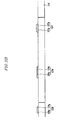
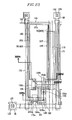
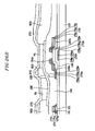
- Fig. 20A and Fig. 20B are sectional views of the TFT array panel shown in Fig. 19 taken along the lines XXa-XXa' and XXb-XXb', respectively.
- Interlayer insulating layers 801 and 802 may be made of an insulating material with a low dielectric constant, such as a-Si:C:O, a-Si:O:F, or SiNx.
- a plurality of pixel electrodes 190, a plurality of connecting members 902, and a plurality of contact assistants 81 and 82 are formed on passivation layer 180.
- a partition 803, an auxiliary electrode 272, a plurality of light emitting members 70, and a common electrode 270 are formed on passivation layer 180 and pixel electrodes 190.
- the etchant of embodiment 2 is preferred, but other etchants, like the etchants of embodiment 1 and embodiment 3, for example, may also be used.
- the gate line When the gate line is patterned with such an etchant, the gate line has a nice profile because the galvanic effect is reduced and etching uniformity is enhanced over the whole substrate due to surface reforming.
- a plurality of gate lines 121 having a plurality of first gate electrodes 124a and a plurality of second gate electrodes 124b are formed, as shown in Fig. 13 through Fig. 14B.
- gate insulating layer 140 is preferably made of silicon nitride with a thickness of about 2,000 ⁇ to 5,000 ⁇ , and the deposition temperature is preferably in a range of about 250°C to 500°C.
- the ITO layer is etched with the same etchant and etching condition as those used in forming the gate lines and the data lines, which is preferably the etchant of embodiment 2.
- Pixel electrodes 190 have side slopes of an angle between approximately 40 degrees and 50 degrees and have CD skew from about 0.2 ⁇ to 0.3 ⁇ .
- a partition 803 and an auxiliary electrode 272 can be formed using only a single photolithography step.
Landscapes
- Chemical & Material Sciences (AREA)
- Engineering & Computer Science (AREA)
- Materials Engineering (AREA)
- Organic Chemistry (AREA)
- Chemical Kinetics & Catalysis (AREA)
- General Chemical & Material Sciences (AREA)
- Mechanical Engineering (AREA)
- Metallurgy (AREA)
- Inorganic Chemistry (AREA)
- Thin Film Transistor (AREA)
- Liquid Crystal (AREA)
- Internal Circuitry In Semiconductor Integrated Circuit Devices (AREA)
- Weting (AREA)
- Electroluminescent Light Sources (AREA)
- ing And Chemical Polishing (AREA)
- Electrodes Of Semiconductors (AREA)
Abstract
Description
- This application claims priority from Korean Patent Application No. 10-2004- 0088809 that was filed in the Korean Intellectual Property Office on November 3, 2004, the disclosure of which is incorporated in its entirety by reference herein.
- The present disclosure relates to an etchant for conductive materials and a method for manufacturing thin film transistor array panels using the same.
- Liquid crystal displays (LCDs) are one of the most widely used types of flat panel displays. An LCD includes a liquid crystal (LC) layer interposed between two panels that include field-generating electrodes. The LCD displays images by applying voltages to the field-generating electrodes to generate an electric field in the LC layer, which orients LC molecules in the LC layer to adjust the polarization of incident light.
- An LCD arranged such that one panel has a plurality of pixel electrodes in a matrix and the other panel has a common electrode currently dominates the LCD market.
- The LCD displays images by applying a different voltage to each pixel electrode. For this purpose, thin film transistors (TFTs), which have three terminals to switch voltages applied to the pixel electrodes, are connected to the pixel electrodes, gate lines that transmit signals for controlling the TFTs, and data lines that transmit voltages applied to the pixel electrodes, are formed on a thin film transistor array panel.
- A TFT is a switching element for transmitting image signals from the data lines to the pixel electrodes in response to scanning signals from the gate lines.
- The TFT is applied to an active matrix organic light emitting display as a switching element for controlling respective light emitting elements.
- Given the increasing size of LCDs, a material having low resistivity is urgently required since the lengths of the gate and data lines also increase along with the LCD size.
- Since a metal having low resistivity has weak chemical resistance, however, such a metal is vulnerable to an etchant. Accordingly, signal lines including a plurality of metal layers, at least one of which has low resistivity, often have defective profiles that include undercut and overhang.
- Conductor patterns like the gate lines, data lines, and pixel electrodes of a TFT array panel are formed through deposition of conductive materials and photo-etchings. Often, the materials of the conductive patterns are different from each other. Generally, different materials require different etchants and etching conditions. Such variations of etchants and etching conditions complicate the manufacturing process and increase overall manufacturing costs.
- It is an object of the present invention to provide an etchant for conductive materials that produces conductive patterns having a nice profile, simplifies the manufacturing process, and thereby reduces manufacturing costs,
- The present invention provides an etchant for conductive materials that contains about 65wt% to about 75wt% of phosphoric acid, about 0.5wt% to about 15wt% of nitric acid, about 2wt% to about 15wt% of acetic acid, about 0.1wt% to about 8.0wt% of a potassium compound, and deionized water for the residual quantity.
- The present invention provides an alternative etchant wherein the potassium compound includes potassium nitrate (KNO3) and potassium acetate (KC2H3O2).
The present invention also provides a method for manufacturing a thin film transistor array panel, including: forming a gate line having a gate electrode on an insulating substrate; depositing in sequence a gate insulating layer, and a semiconductor layer on the gate line; forming a drain electrodeon the gate insulating layer and the semiconductor layer; forming a data line having a source electrode on the gate insulating layer and the semiconductor layer such that a gap is disposed between the drain electrode and the source electrode; and forming a pixel electrode connected to the drain electrode, wherein at least one of the gate line, the data line, the drain electrode, and the pixel electrode is formed by photo-etching using an etchant comprising about 65wt% to about 75wt% of phosphoric acid, about 0.5wt% to about 15wt% of nitric acid, about 2wt% to about 15wt% of acetic acid, about 0.1wt% to about 8.0wt% of a potassium compound, and deionized water. - Fig. 1 is a layout view of a TFT array panel for an LCD according to an embodiment of the present invention.
- Fig. 2 is a sectional view of the TFT array panel shown in Fig. 1 taken along the line II-II.
- Fig. 3A, Fig. 4A, Fig. 5A, and Fig. 6A are layout views sequentially illustrating the intermediate steps of a method of manufacturing a TFT array panel for an LCD shown in Fig. 1 and Fig. 2;
- Fig. 3B is a sectional view of the TFT array panel shown in Fig. 3A taken along the line IIIb-IIIb'.
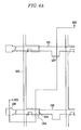
- Fig. 4B is a sectional view of the TFT array panel shown in Fig. 4A taken along the line IVb-IVb' in the step following the step shown in Fig. 3B.
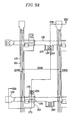
- Fig. 5B is a sectional view of the TFT array panel shown in Fig. 5A taken along the line Vb-Vb' in the step following the step shown in Fig. 4B.
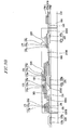
- Fig. 6B is a sectional view of the TFT array panel shown in Fig. 6A taken along the line VIb-VIb' in the step following the step shown in Fig. 5B.
- Fig. 7 is a layout view of a TFT array panel for an LCD according to another embodiment of the present invention.
- Fig. 8 is a sectional view of the TFT array panel shown in Fig. 7 taken along the line VIII-VIII'.
- Fig. 9A and Fig. 10A are layout views of the TFT array panel shown in Fig. 7 and Fig. 8 in intermediate steps of a manufacturing method according to another embodiment of the present invention.
- Fig. 9B is a sectional view of the TFT array panel shown in Fig. 9A taken along the line IXb-IXb'.
- Fig. 10B is a sectional view of the TFT array panel shown in Fig. 10A taken along the line Xb-Xb'.
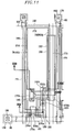
- Fig. 1 is a layout view of a TFT array panel for an OLED according to yet another embodiment of the present invention.
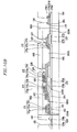
- Fig. 12A and Fig. 12B are sectional views of the TFT array panel shown in Fig. 11 taken along the line XIIa-XIIa' and the line XIIb-XIIb', respectively.
- Fig. 13, Fig. 15, Fig. 17, Fig. 19, Fig. 21, Fig. 23, and Fig. 25 are layout views of the TFT array panel shown in Fig. 11, Fig. 12A, and Fig. 12B in intermediate steps of a manufacturing method according to yet another embodiment of the present invention.
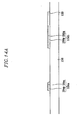
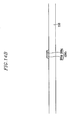
- Fig. 14A and Fig. 14B are sectional views of the TFT array panel shown in Fig. 13 taken along the lines XIVa-XIVa' and XIVb-XIVb', respectively.
- Fig. 16A and Fig. 16B are sectional views of the TFT array panel shown in Fig. 15 taken along the lines XVIa-XVIa' and XVIb-XVIb', respectively.
- Fig. 18A and Fig. 18B are sectional views of the TFT array panel shown in Fig. 17 taken along the lines XVIIIa-XVIIIa' and XVIIIb-XVIIIb', respectively.
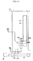
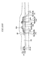
- Fig. 20A and Fig. 20B are sectional views of the TFT array panel shown in Fig. 19 taken along the lines XXa-XXa' and XXb-XXb', respectively.
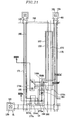
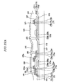
- Fig. 22A and Fig. 22B are sectional views of the TFT array panel shown in Fig. 21 taken along the lines XXIIa-XXIIa' and XXIIb-XXIIb', respectively.
- Fig. 24A and Fig. 24B are sectional views of the TFT array panel shown in Fig. 23 taken along the lines XXIVa-XXIVa' and XXIVb-XXIVb', respectively.
- Fig. 26A and Fig. 26B are sectional views of the TFT array panel shown in Fig. 25 taken along the lines XXVIa-XXVIa' and XXVIb-XXVIb', respectively.
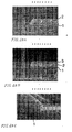
- Fig. 27A is a sectional picture of a gate line patterned with the etchant of
reference 1. - Fig. 27B is a sectional picture of a data line patterned with the etchant of
reference 3. - Fig. 28A is a sectional picture of a gate line patterned with the etchant of
embodiment 2. - Fig. 28B is a sectional picture of a data line patterned with the etchant of
embodiment 2. - Fig. 28C is a sectional picture of a pixel electrode patterned with the etchant of
embodiment 2. - Preferred embodiments of the present invention will now be described more fully hereinafter with reference to the accompanying drawings, in which embodiments of the invention are shown. The present invention may, however, be embodied in different forms and should not be construed as being limited to the embodiments set forth herein. Rather, these embodiments are provided so that this disclosure will be thorough and complete, and will fully convey the scope of the invention to those skilled in the art.
- In the drawings, the thickness of layers, films, and regions are exaggerated for clarity. Like numerals refer to like elements throughout. The position of elements may be described in reference to their orientation in the figure, e.g. upward being towards the top of the figure. It will be understood that when an element such as a layer, film, region, or substrate is referred to as being "on" another element, it can be directly on the other element or intervening elements may also be present.
- Profiles of gate lines, data lines, and pixel electrodes, which are patterned with etchants according to embodiments of the present invention, and etching uniformity of the etchants, are measured.
- Six etchants are prepared. Ingredients of the etchants are listed in Table 1.
Table 1 wt% Phosphoric acid Nitric acid Acetic acid KNO3 KC2H3O2 NH4HS C7H9NO2 Deionized water Embodiment 1 67 6 10 1 1 - - 15 Embodiment 267 6 10 1 1 1 1 13 Embodiment 373 8,5 7 2 2 - - - 7.5 Reference 163 3 15.5 - - - - - 18.5 Reference 264 5 10 - - - - - 21 Reference 363 3 10 4.5 4.5 4.5 4.5 6 - Six substrates for gate lines were prepared, which had a lower conductive layer of aluminum-neodymium (Al-Nd) and an upper conductive layer of molybdenum nitride (MoN). Six substrates for data lines were also prepared, which had a lower conductive layer of molybdenum niobium (Mo-Nb), a middle conductive layer of aluminum-neodymium (Al-Nd), and an upper conductive layer of Mo-Nb on the middle conductive layer. Finally, six substrates for pixel electrodes were prepared, which had an indium zinc oxide (IZO) layer.
- Then, photoresist was coated on the substrates and was illuminated with light through a photo-mask. Next, the illuminated photoresist was developed.
- Next, six spray type etch chambers filled with the six etchants of Table 1 were prepared. The etch chambers had an inner temperature of about 30°C to 45°C. In the present test, all of the etch chambers were set to have a temperature of about 40°C.
- In each chamber, three substrates composed of a substrate for gate lines, a substrate for data lines, and a substrate for pixel electrodes were disposed therein for etching the conductive layers. Etching time was adjusted from approximately 30 seconds to 200 seconds. Substrates having the same conductive layer were etched for the same period of time.
- After etching, the substrates were cleansed with deionized water and then dried.
- Next, after stripping the photoresist, sectional profiles of the etched conductive layers were inspected with a scanning electron microscope (SEM).
- The results were as follows.
- Conductive layers etched with the etchants of
embodiments embodiment 2 showed especially good profiles. - In contrast, conductive layers etched with the etchants of
references - Conductive layers etched with the etchant of
reference 3 showed a bad profile having recessed Mo layers, opposite to the conductive layers etched with the etchant ofreferences - Looking at Fig. 27A, the gate line patterned with the etchant of
reference 1 has an undercut that is formed due to an etch rate discrepancy between the lowerconductive layer 1 of Al-Nd and the upperconductive layer 2 of MoN. Since Al-Nd is etched faster than MoN, the lowerconductive layer 1 is recessed. - Referring to Fig. 27B, the data line patterned with the etchant of
reference 3 has a bad profile that is formed due to a discrepancy of etch speed between the middleconductive layer 2 of Al-Nd and the lowerconductive layer 1 and the upperconductive layer 3 of Ma-Nb. (Thereference numeral 4 in Fig. 27B represents the photoresist layer). Contrary toreference 1, the etchant ofreference 3 etches Mo-Nb faster than the Al-Nd. Accordingly, the lowerconductive layer 1 and the upperconductive layer 3 are recessed. Slope angle of the lines and CD skew cannot be measured due to the bad profile. Furthermore, severe stains are generated in all conductive layers. - On the other hand, referring to Figs. 28A, 28B, and 28C, all conductive layers (gate lines, data lines, and pixel electrodes) etched with the etchant of
embodiment 2 have a good side slope and critical dimension (CD) without undercut or overhang. In particular, the gate line of double layers (Fig. 28A) and the data line of triple layers (Fig. 28B) do not suffer a profile degradation that may occur when there is an etch rate discrepancy between a lower layer and an upper layer. Furthermore, the etchant ofembodiment 2 etches the pixel electrode material as well as the materials of the gate line and the data line. Precisely, the gate line and the data line have side slopes of an angle between 60 degrees and 80 degrees and have a CD skew from about 1.0□ to 1.5□. The pixel electrode has side slopes of an angle about 50 degrees and has a CD skew of from about 0.2□ to 0.3□. The etchant ofembodiment 2 uniformly etches the conductive layers throughout the whole area of the substrates without inducing stains. - As described above, an etchant according to an embodiment of the present invention further contains a potassium compound and/or a basic nitrogen compound along with phosphoric acid, nitric acid, and acetic acid to stabilize the profile of the conductive layers and to enhance etching uniformity.
- In general, a conductor having two or more layers suffers profile degradation due to etch rate discrepancy. Double layer or triple layer conductive layers including a Mo layer and an Al layer may suffer serious profile degradation due to a galvanic effect. The galvanic effect exists when oxidation and reduction results in metals having different electrical potentials are disposed in an electrolyte solution. A metal having a relatively positive potential works as a cathode and tends to be reduced, while the other metal having a relatively negative potential works as an anode and tends to be oxidized. The galvanic effect reduces the etching rate (eroding speed) of the cathode metal and increases the etching speed of the anode metal. Accordingly, the Al layer of multi-metal layers, including an Al layer and a Mo layer, which works as an anode, is etched much faster than the Mo layer, which acts as a cathode.
- An etchant according to an embodiment of the present invention further contains a potassium compound and/or a basic nitrogen compound along with phosphoric acid, nitric acid, and acetic acid to reduce the galvanic effect.
- A potassium compound and a basic nitrogen compound reduce the galvanic effect by restraining migration of electrons between different metals. However, when an etchant contains too much of the potassium compound or the basic nitrogen compound, the galvanic effect may be over-restrained and induce a reversal of etching rate. Accordingly, the proportion of the potassium compound and the basic nitrogen compound is required to be adjusted for an appropriate galvanic effect.
- An etchant according to the present invention preferably contains about 0.1wt% to 8wt% of the potassium compound and/or the basic nitrogen compound. When an etchant contains less than 0.1 wt% of the potassium compound and/or the basic nitrogen compound the effect of restraining the galvanic effect is not shown, much like in the etchant of
reference 1. When an etchant contains more than 8wt% of the potassium compound and/or the basic nitrogen compound the galvanic effect may be over-restrained and induce a reversal of etching rate as described above. Such an etchant etches the Mo layer faster than the A1 layer, like in the etchant ofreference 3, and induces profile degradation. - When a conductive layer on a large size substrate is patterned with a conventional etchant, the conductive layer is irregularly etched due to an etch rate discrepancy between a center portion and edge portions.
- An etchant according to an embodiment of the present invention further contains a potassium compound and/or a basic nitrogen compound along with phosphoric acid, nitric acid, and acetic acid to reform surface conditions of the target layer. Accordingly, etching is uniformly performed on the whole area. This effect can be seen in Fig. 27A through Fig. 28C.
- An etchant according to the present invention can be applied to conductive layers like pattern gate lines, data lines, and pixel electrodes regardless of the number of layers. All conductive layers etched with an etchant of the present invention have a good profile. Accordingly, costs are reduced and the manufacturing process is simplified, which thereby increases production efficiency. Furthermore, an etchant according to the present invention uniformly etches conductive layers throughout the whole area without inducing stains, which enhances product quality.
- In the above descriptions, Al-Nd, MoN, Mo-Nb, and IZO are exemplified for the test. However, an etchant according to the present invention may etch materials including Al or Mo, as well as indium tin oxide (ITO). As known to persons of ordinary skill in the art, an etchant according to the present invention could be used to etch other conductive materials.
- Now, a TFT array panel and a manufacturing method thereof using the etchant of
embodiment 2 will be described in detail with reference to the accompanying drawings. - As shown in Fig. 1 and Fig. 2, a plurality of
gate lines 121 for transmitting gate signals are formed on an insulatingsubstrate 110.Gate lines 121 are mainly formed in the horizontal direction and partial portions thereof become a plurality ofgate electrodes 124. Also,gate lines 121 include portions that extend in a lower direction that become a plurality ofexpansions 127. Anend portion 129 ofgate line 121 has an expanded width for connecting with an external device such as a driving circuit. -
Gate line 121 haslower layers upper layers Lower layers Upper layers - The lateral sides of
upper layers lower layers substrate 110, and the inclination angle thereof ranges from about 30 degrees to 80 degrees. - A
gate insulating layer 140 preferably made of silicon nitride (SiNx) can be formed ongate lines 121. - A plurality of
semiconductor stripes 151, preferably made of hydrogenated amorphous silicon (abbreviated to "a-Si"), can be formed ongate insulating layer 140. Eachsemiconductor stripe 151 extends substantially in the longitudinal direction and has a plurality ofprojections 154 branched out towardsgate electrodes 124. The width of eachsemiconductor stripe 151 becomes large near thegate lines 121 to cover large areas thereof. - A plurality of
ohmic contact stripes 161 andislands 165, preferably made of silicide or n+ hydrogenated a-Si heavily doped with n-type impurity, can be formed on thesemiconductor stripes 151. Eachohmic contact stripe 161 has a plurality ofprojections 163 formed in pairs withohmic contact islands 165 onprojections 154 of thesemiconductor stripes 151. - The edge surfaces of
semiconductor stripes 151 andohmic contacts - A plurality of
data lines 171, a plurality ofdrain electrodes 175, and a plurality ofstorage capacitor conductors 177 are formed onohmic contacts gate insulating layer 140. -
Data lines 171, for transmitting data voltages, extend substantially in the longitudinal direction and crossgate lines 121 to define the pixel areas arranged in a matrix.Data lines 171 have a plurality of branches, which project towardrespective drain electrodes 175, that form a plurality ofsource electrodes 173.Data lines 171 further have anend portion 179 of an enlarged width. Each pair of thesource electrodes 173 and thedrain electrodes 175 are separated from each other over thegate electrodes 124 to thereby oppose one another. -
Data line 171,drain electrode 175, andstorage capacitor conductor 177 may comprisefirst layers second layers third layers first layers third layers second layers first layers third layers second layers data line 171 has a low resistivity and the Al or Al-alloy layer is prevented from contacting the semiconductor and the pixel electrodes, which may cause a bad contact. Accordingly, degrading of TFTs caused by bad contact is efficiently prevented. -
Gate electrode 124,source electrode 173, anddrain electrode 175, along withprojection 154 ofsemiconductor stripe 151, forms a TFT having a channel formed in theprojection 154 disposed between thesource electrode 173 and thedrain electrode 175. A portion ofstorage capacitor conductor 177 may overlapexpansion 127 ofgate line 121. -
Data lines 171,drain electrodes 175, and thestorage capacitor conductor 177 have edge surfaces that are tapered at an angle in a range from about 30 degrees to 80 degrees. -
Ohmic contacts semiconductor stripe 151 anddata line 171 as well as betweendrain electrode 175 andsemiconductor stripe projection 154 in order to reduce contact resistance therebetween. -
Semiconductor stripe 151 is partially exposed at an area betweensource electrode 173 anddrain electrode 175, and at other areas not covered bydata line 171 ordrain electrode 175. Most ofsemiconductor stripe 151 is narrower thandata line 171, butsemiconductor stripe 151 broadens near the area wheresemiconductor stripe 151 crossesgate line 121 to prevent disconnection ofdata line 171. - A
passivation layer 180 is provided ondata line 171,drain electrode 175,storage capacitor conductor 177, and the exposed region ofsemiconductor stripe 151.Passivation layer 180 can be made of an organic material having substantial planarization properties and photosensibility or can be made if an insulating material with a low dielectric constant such as a-Si:C:O or a Si:O:F, for example.Passivation layer 180 may be formed by plasma enhanced chemical vapor deposition (PECVD).Passivation layer 180 can be structured in a way that an insulating layer made of SiNx or SiO2 is additionally formed under the organic material layer to prevent the organic material ofpassivation layer 180 from contacting portions ofsemiconductor stripes 151 exposed betweendata line 171 anddrain electrode 175. - A plurality of contact holes 181, 185, 187, and 182 are formed in
passivation layer 180 to expose anend portion 129 ofgate line 121,drain electrode 175,storage capacitor conductor 177, and anend portion 179 ofdata line 171, respectively. - A plurality of
pixel electrodes 190 and a plurality ofcontact assistants passivation layer 180. - Since
pixel electrode 190 is physically and electrically connected to drainelectrode 175 andstorage capacitor conductor 177 through respective contact holes 185 and 187,pixel electrode 190 receives the data voltage fromdrain electrode 175 and transmits it to thestorage capacitor conductor 177. -
Pixel electrode 190, to which the data voltage is applied, generates an electric field with a common electrode (not illustrated) of the opposite panel (not illustrated), to which a common voltage is applied, to orient LC molecules in the LC layer to change the polarization of incident light. - Also,
pixel electrode 190 and the common electrode form a capacitor to store a voltage after the TFT is turned off. This capacitor will be referred to as an "LC capacitor." To enhance the voltage storage ability, another capacitor is provided, which is connected with the LC capacitor in parallel and will be referred to as a "storage capacitor." The storage capacitor is formed at an overlapping portion of thepixel electrode 190 and theadjacent gate line 121, which will be referred to as a "previous gate line."Gate line expansion 127 is provided to ensure the largest possible overlap dimension and, thus, increase the storage capacity of the storage capacitor.Storage capacitor conductor 177 is connected topixel electrode 190 and overlapsexpansion 127, and is provided at the bottom ofpassivation layer 180 so thatpixel electrode 190 becomes close to theprevious gate line 121. -
Optional contact assistants line end portion 129 and data lineend portion 179, respectively.Contact assistants end portions - A method of manufacturing a TFT array panel will now be described in detail with reference to Fig. 3A through Fig. 6B, as well as Fig. 1 and Fig. 2.
- At first, as shown in Fig. 3A and Fig. 3B, metal layers are formed on an insulating
substrate 110. - The metal layer is deposited by a Co-sputtering. Two targets are installed in a same sputtering chamber for the Co-sputtering. One target can be made of Al-Nd. The other target can be made of Mo. Here, the Al-Nd target preferably contains 2wt% ofNd.
- The Co-sputtering is performed as follows.
- At first, power is applied to the Al-Nd target while no power is applied to the Mo target to deposit a lower layer of Al-Nd. The thickness of the lower layer is preferably 2,500Å but may be varied from approximately 1,000Å to 5,000Å
- Next, power is applied to the Mo target and not applied to the Al-Nd target to deposit an upper layer. The thickness of the upper layer is preferably 1,000Å but may be varied from approximately 50Å to 2,000Å
- Then, photoresist is coated on the upper layer and is illuminated with a light through a photo-mask to develop the photoresist.
- The upper and lower layers are simultaneously etched to form a plurality of gate lines 121. The etching is performed at a temperature between about 35°C and 45°C for approximately 30 seconds to 200 seconds by spraying an etchant on the substrate.
- The proportions of the etchant components may be varied in approximate ranges of 65wt% to 75wt% of phosphoric acid, 0.5wt% to 15wt% of nitric acid, 2wt% to 15wt% of acetic acid, 0.1 wt% to 8.0wt% of a potassium compound, and water for the residual quantity. As previously noted, when 0.1 wt% to 8.0 wt% of a basic nitrogen compound is added to the etchant, conductive layers may have a better profile when etched.
- When the gate line is patterned with such an etchant, the gate line has a nice profile because the galvanic effect is reduced and etching uniformity is enhanced over the whole substrate due to surface reforming.
- Through the above described processes, as shown in Fig. 3A and Fig. 3B, a plurality of
gate lines 121 having a plurality ofgate electrodes 124,expansions 127, and endportions 129 are formed. - Referring to Fig. 4A and Fig. 4B, after sequential deposition of a
gate insulating layer 140, an intrinsic a-Si layer, and an extrinsic a-Si layer, the extrinsic a-Si layer and the intrinsic a-Si layer are photo-etched to form a plurality ofextrinsic semiconductor stripes 161 and a plurality ofintrinsic semiconductor stripes 151 havingrespective projections Gate insulating layer 140 is preferably made of silicon nitride with a thickness of about 2,000Å to about 5,000Å, and the deposition temperature is preferably in a range from about 250 °C to 500 °C. - Next, a first layer of Mo-Nb, a second layer of Al-Nd, and a third layer of Mo-Nb can be sequentially deposited on
extrinsic semiconductor stripes 161. The thickness of the first layer is preferably in a range from about 50Å to 2,000Å. The second layer is preferably between about 1,000Å and 5,000Å. The thickness of the third layer is preferably between about 50Å and 2,000Å. The sputtering temperature is preferably about 150°C. - Then, photoresist is coated on the third layer and is illuminated with a light through a photo-mask to develop the photoresist.
- The first layer, the second layer, and the third layer are simultaneously etched with the etchant of
embodiment 2 to form a plurality ofdata lines 171 anddrain electrodes 175. The etching is performed at a temperature between about 35°C and 45°C for about 30 seconds to 200 seconds by spraying an etchant on the substrate. - As noted before, the data line patterned using such an etchant has a nice profile because the galvanic effect is reduced and etching uniformity is enhanced over the whole substrate due to surface reforming.
- Through the above described processes, as shown in Fig. 5A and Fig. 5B, a plurality of
data lines 171 having a plurality ofsource electrodes 173, a plurality ofdrain electrodes 175,end portions 179, andstorage capacitor conductors 177 are formed. - Next, portions of the
extrinsic semiconductor stripes 161, which are not covered by thedata lines 171 ordrain electrodes 175, are removed by etching to complete a plurality ofohmic contacts intrinsic semiconductor stripes 151. Oxygen plasma treatment may follow thereafter in order to stabilize the exposed surfaces ofsemiconductor stripes 151. - Looking at Fig. 6A and Fig. 6B, a
passivation layer 180 is deposited and dry etched along with thegate insulating layer 140 to form a plurality of contact holes 181, 185, 187, and 182.Gate insulating layer 140 and thepassivation layer 180 are preferably etched under an etch condition having substantially the same etch ratio for bothgate insulating layer 140 andpassivation layer 180. - When the
passivation layer 180 is made of a photosensitive material, the contact holes 181, 185, 187, and 182 can be formed only by a photolithography process. - Next, an ITO layer having a thickness of about 400Å to 1500Å is deposited on the
passivation layer 180. - Then, photoresist is coated on the ITO layer and is illuminated with a light through a photo-mask to develop the photoresist.
- Next, the ITO layer is etched with the etchant of
embodiment 2 to form a plurality ofpixel electrodes 190. The etching is performed at a temperature between about 35°C and 45°C for approximately 30 seconds to 200 seconds by spraying an etchant on the substrate. - As a result,
pixel electrodes 190 andcontact assistants substrate 110 at an angle of about 50 degrees. - In the present invention, since
gate lines 121,data lines 171 anddrain electrodes 175, andpixel electrodes 190 are patterned with the same etchant and etching conditions, costs are saved and manufacturing processes are simplified. Furthermore, all conductive layers etched with an etchant of the present invention have a good profile. - In the above descriptions, Al-Nd, Mo, Mo-Nb, and IZO are exemplified as conductive materials for signal lines and pixel electrodes. However, an etchant according to the present invention may etch all conductive materials including Al or Mo metals, as well as ITO. An etchant according to the present invention may also etch other conductive materials.
- Multi-layer signal lines are exemplified in the present embodiment but single layer signal lines may be applied.
- As shown in Fig. 7 and Fig. 8, another embodiment of the invention illustrates a thin film transistor array panel having color filters. The pixel electrode panel has a similar structure as the one previously described and is formed in a similar manner.
- Here,
color filters data line 171,drain electrode 175, andstorage capacitor conductor 177. Color filters 230R, 230G, and 230B are formed along pixel columns that are partitioned bydata lines 171. The red, green, andblue color filters - Color filters 230R, 230G, and 230B are not formed on the end portions of
gate lines 121 anddata lines 171, which are connected to external circuits. Twoadjacent color filters data lines 171. Accordingly, light leakage that may arise around a pixel area is prevented by the overlapping ofcolor filters blue color filters data line 171 to overlap each other. - A first
interlayer insulating layer 801 is formed under thecolor filters semiconductor protrusion 154. A secondinterlayer insulating layer 802 is formed on top of thecolor filters -
Interlayer insulating layers - As described above, when the
color filters data line 171, the opposite panel may have only a common electrode. Accordingly, assembly of the TFT panel and the opposite panel is easy and the aperture ratio increases. - In second
interlayer insulating layer 802, a plurality of contact holes 181, 185, 187, and 182 are formed to expose gateline end portion 129,drain electrode 175,storage capacitor conductor 177, and data lineend portion 179 respectively. - A plurality of
pixel electrodes 190 and a plurality ofcontact assistants 82, which are made of IZO or ITO, are formed on secondinterlayer insulating layer 802. - As before
pixel electrode 190 is physically and electrically connected with thedrain electrode 175 and thestorage capacitor conductor 177 through the contact holes 185 and 187, respectively, and, thus,pixel electrode 190 still receives the data voltage fromdrain electrode 175 and transmits it tostorage capacitor conductor 177. - A method of manufacturing a TFT array panel will now be described with reference to Fig. 9A through Fig. 10B, which is similar to the previously described method as shown in Fig. 3A through 6B.
- In this method, however, organic photo-resist materials respectively containing pigments of red, green, and blue can be coated and patterned by a photo process to form a plurality of
color filters interlayer insulating layer 801 made of an inorganic insulating material such as silicon nitride (SiNx) or silicon oxide (SiO2) is formed on thedata lines 171 anddrain electrodes 175 before forming thecolor filters openings drain electrode 175 andstorage capacitor conductor 177 are simultaneously formed. - Referring to Figs. 10A and 10B, a second
interlayer insulating layer 802 is formed by the coating of an organic insulating film having a low dielectric constant and a good flatness characteristic, or by the PECVD of a low dielectric insulating material such as a-Si:C:O or a-Si:O:F having a dielectric constant lower than about 4.0 - Thereafter, first insulating
layer 801 and secondinterlayer insulating layer 802 may be photo-etched to form a plurality of contact holes 181, 182, 185, and 187. Here, contact holes 185 and 187 exposingdrain electrode 175 andstorage capacitor conductor 177 are formed in theopenings color filters - Finally, as shown in Fig. 7 and Fig. 8, a plurality of
pixel electrodes 190 and a plurality ofcontact assistants Pixel electrodes 190 are connected to drainelectrodes 175 andstorage capacitor conductor 177 through respective contact holes 185 and 187. -
Pixel electrodes 190 may be formed using the same etchant and etching conditions asgate lines 121 anddata lines 171. -
Pixel electrodes 190 can have side slopes of an angle between about 40 degrees and 50 degrees and have a CD skew of from about 0.2□ to 0.3□. - Now, a TFT panel for an active matrix organic light emitting display (AM-OLED) according to another embodiment of the present invention will be described in reference to Fig. 12A, Fig. 12B and
- A plurality of gate conductors that include a plurality of
gate lines 121, including a plurality offirst gate electrodes 124a and a plurality ofsecond gate electrodes 124b, are formed on an insulatingsubstrate 110 such as transparent glass. -
Gate lines 121 that transmit gate signals extend substantially in a transverse direction and are separated from each other.First gate electrode 124a protrudes upward.Gate lines 121 may extend to be connected to a driving circuit (not shown) integrated onsubstrate 110, or they may have an end portion (not shown) having a large area for connection with another layer or an external driving circuit mounted onsubstrate 110 or on another device such as a flexible printed circuit film (not shown) that may be attached tosubstrate 110. - Each of the
second gate electrodes 124b is separated fromgate lines 121 and includes astorage electrode 133 extending substantially in a longitudinal direction between two adjacent gate lines 121. - The
first gate electrodes 124a, thesecond gate electrodes 124b, andstorage electrodes 133 can have lower layers 124ap, 124bp, and 133p and upper layers 124aq, 124bq, and 133q. Lower layers 124ap, 124bp, and 133p can be made of a material including Al, like Al itself or Al-Nd. Upper layers 124aq, 124bq, and 133q can be made of a material including Mo, like Mo itself or MoN. - In addition, the lateral sides of
gate conductors substrate 110 at an angle that ranges from about 30 degrees to 80 degrees. - A
gate insulating layer 140, preferably made of SiNx, is formed ongate conductors - A plurality of
semiconductor stripes 151 andislands 154b, preferably made of hydrogenated amorphous silicon (abbreviated to "a-Si") or polysilicon, are formed ongate insulating layer 140. Eachsemiconductor stripe 151 extends substantially in the longitudinal direction and has a plurality ofprojections 154a branched out towardsfirst gate electrodes 124a. Eachsemiconductor island 154b crosses asecond gate electrode 124b and includes aportion 157 overlappingstorage electrode 133 ofsecond gate electrode 124b. - A plurality of
ohmic contact stripes 161 andohmic contact islands semiconductor stripes 151 andislands 154b. Eachohmic contact stripe 161 has a plurality ofprojections 163a, formed in pairs withohmic contact islands 165a onsemiconductor stripe projections 154a.Ohmic contact islands semiconductor islands 154b. - The lateral sides of the
semiconductor stripes 151 andislands 154b and theohmic contacts - A plurality of data conductors including a plurality of
data lines 171, a plurality ofvoltage transmission lines 172, a plurality offirst drain electrodes 175a, and a plurality ofsecond drain electrodes 175b are formed onohmic contacts gate insulating layer 140. -
Data lines 171 that transmit data signals extend substantially in the longitudinal direction and cross gate lines 121. Eachdata line 171 includes a plurality offirst source electrodes 173a, an end portion having a large area for contact with another layer or an external device. The data lines 171 may be directly connected to a data driving circuit for generating the gate signals that may be integrated onsubstrate 110. -
Voltage transmission lines 172 for transmitting driving voltages extend substantially in the longitudinal direction and cross gate lines 121. Eachvoltage transmission line 172 includes a plurality ofsecond source electrodes 173b.Voltage transmission lines 172 may be connected to each other and overlap thestorage region 157 of thesemiconductor islands 154b. - The first and
second drain electrodes data lines 171 and thevoltage transmission lines 172, and from each other. Each pair of thefirst source electrodes 173a and thefirst drain electrodes 175a are disposed opposite each other with respect to afirst gate electrode 124a, and each pair of thesecond source electrodes 173b and thesecond drain electrodes 175b are disposed opposite each other with respect to asecond gate electrode 124b. - A
first gate electrode 124a, afirst source electrode 173a, and afirst drain electrode 175a, along withsemiconductor stripe projection 154a, form a switching TFT having a channel formed in theprojection 154a disposed between thefirst source electrode 173a and thefirst drain electrode 175a. Meanwhile, asecond gate electrode 124b, asecond source electrode 173b, and asecond drain electrode 175b, along with asemiconductor island 154b, form a driving TFT having a channel formed insemiconductor island 154b disposed between thesecond source electrode 173b and thesecond drain electrode 175b. -
Data conductors first layers second layers third layers second layers first layers third layers second layers first layers third layers - Like
gate conductors data conductors substrate 110, inclined at angles that range from about 30 degrees to 80 degrees. -
Ohmic contacts underlying semiconductor stripes 151 andislands 154b andoverlying data conductors Semiconductor stripes 151 include a plurality of exposed portions that are not covered with thedata conductors - Most of the
semiconductor stripe 151 is narrower thandata line 171, butsemiconductor stripe 151 broadens near an area where thesemiconductor stripe 151 crossesgate line 121 to prevent disconnection of thedata line 171 as mentioned above. -
Passivation layer 180 is formed on thedata conductors semiconductor stripes 151 andislands 154b.Passivation layer 180 is preferably made of an inorganic material, such as SiNx or SiO2, a photosensitive organic material having good flatness characteristics, or a low dielectric insulating material having a dielectric constant lower than 4.0 such as a-Si:C:O or a-Si:O:F formed by PECVD.Passivation layer 180 may also include a lower film of an inorganic insulator and an upper film of an organic insulator. -
Passivation layer 180 has a plurality of contact holes 189, 183, 185, 181, and 182 exposing portions offirst drain electrode 175a,second gate electrode 124b,second drain electrode 175b, and endportions gate line 121 anddata line 171, respectively. - Contact holes 181 and 182 expose gate
line end portions 129 and data lineend portion 179 to connect them with external driving circuits. Anisotropic conductive films are disposed between the output terminals of the external driving circuit and endportions substrate 110, contact holes are not formed. When gate driving circuits are directly fabricated onsubstrate 110 and data driving circuits are formed as separate chips, onlycontact hole 181 exposing dataline end portion 179 is formed. - A plurality of
pixel electrodes 190, a plurality of connecting members 902, and a plurality ofcontact assistants passivation layer 180. -
Pixel electrode 190 is connected tosecond drain electrode 175b throughcontact hole 185. Connectingmember 192 connectsfirst drain electrode 175a andsecond gate electrode 124b through respective contact holes 189 and 183.Contact assistants end portion 179 throughcontact holes -
Pixel electrode 190, connectingmember 192, andcontact assistants - A
partition 803, anauxiliary electrode 272, a plurality of light emittingmembers 70, and acommon electrode 270 are formed onpassivation layer 180 andpixel electrodes 190. -
Partition 803 is made of an organic or inorganic insulating material that frames organic light emitting cells.Partition 803 is formed along boundaries ofpixel electrode 190 and defines a space that can be filled with an organic light emitting material. -
Light emitting member 70 is disposed onpixel electrode 190 and is surrounded bypartition 803.Light emitting member 70 is made of a light emitting material that emits red, green, or blue light. Red, green, and bluelight emitting members 70 are sequentially and repeatedly disposed. -
Auxiliary electrode 272 has substantially the same planar pattern aspartition 803.Auxiliary electrode 272 contactscommon electrode 270 to reduce resistance thereof. -
Common electrode 270, which is made of a metal such as Al having low resistivity is formed onpartition 803,auxiliary electrode 272, andlight emitting member 70. This embodiment illustrates a back emitting OLED. However, a front emitting OLED or dual-side emitting OLED can be produced whencommon electrode 270 is made of a transparent conductor such as ITO or IZO. - A method of manufacturing the TFT array panel shown in Fig. 11 through Fig. 12B according to an embodiment of the present invention will be now described in detail with reference to Fig. 13 through Fig. 26B.
- First, as shown in Fig. 13 through Fig. 14B, gate metal layers are deposited on
substrate 110. A single metal layer may be formed to form gate lines. However, in the present embodiment, the gate metal layers include a lower layer of Al-alloy and an upper layer of Mo-alloy. Here, the lower layer has a thickness between 1,000Å and 5,000Å. The upper layer has a thickness between 50Å and 2,000Å. - The upper and lower layers may be simultaneously etched to form a plurality of gate lines 121. The etching is performed at a temperature between approximately 35°C and 45°C for about 30 seconds to 200 seconds by spraying an etchant on the substrate.
- The etchant of
embodiment 2 is preferred, but other etchants, like the etchants ofembodiment 1 andembodiment 3, for example, may also be used. - When the gate line is patterned with such an etchant, the gate line has a nice profile because the galvanic effect is reduced and etching uniformity is enhanced over the whole substrate due to surface reforming.
- Through the above described processes, a plurality of
gate lines 121 having a plurality offirst gate electrodes 124a and a plurality ofsecond gate electrodes 124b are formed, as shown in Fig. 13 through Fig. 14B. - Referring to Fig. 15 through Fig. 16B, after a sequential deposition of
gate insulating layer 140, an intrinsic a-Si layer, and an extrinsic a-Si layer, the extrinsic a-Si layer and the intrinsic a-Si layer are photo-etched to form a plurality ofextrinsic semiconductor stripes 164 and a plurality ofintrinsic semiconductor stripes 151 andislands 154b, includingprojections 154a, ongate insulating layer 140.Gate insulating layer 140 is preferably made of silicon nitride with a thickness of about 2,000Å to 5,000Å, and the deposition temperature is preferably in a range of about 250°C to 500°C. - Referring to Fig. 17 through Fig. 18B, a first layer of Mo-alloy, a second layer of Al (or Al-alloy), and a third layer of Mo-alloy can be sequentially deposited on
extrinsic semiconductor stripes 164. The three layers are etched using a photoresist (not shown) to form a plurality of data conductors that includes a plurality ofdata lines 171 includingfirst source electrodes 173a, a plurality ofvoltage transmission lines 172, which includesecond source electrodes 173b, and a plurality offirst drain electrodes 175a andsecond drain electrodes 175b. - Here, the triple
layered data lines 171,second drain electrodes 175b, andvoltage transmission lines 172 can be formed by using the same etchant and etching conditions as those used to form gate lines 121. As a result,data lines 171,second drain electrodes 175b, andvoltage transmission lines 172 have side slopes of an angle between approximately 40 degrees and 60 degrees relative tosubstrate 110 and have a nice profile without undercut or overhang.Data lines 171,second drain electrodes 175b, andvoltage transmission lines 172 do not have stains. - Before or after removing the photoresist, portions of the
extrinsic semiconductor stripes 164, which are not covered withdata conductors ohmic contact stripes 161, which includeprojections 163a, and a plurality ofohmic contact islands intrinsic semiconductor stripes 151 andislands 154b. - Oxygen plasma treatment may follow thereafter in order to stabilize the exposed surfaces of
semiconductor stripes 151. - Referring to Fig. 19 through Fig. 20B, a
passivation layer 180 can be deposited and patterned to form a plurality of contact holes 189, 185, 183, 181, and 182 that exposefirst drain electrode 175a,second drain electrode 175b,second gate electrode 124b, gateline end portion 129, and data lineend portion 179, respectively. - Referring to Fig. 21 through Fig. 22B, a plurality of
pixel electrodes 190, a plurality of connectingmembers 192, andcontact assistants passivation layer 180 with ITO or IZO. - The ITO layer is etched with the same etchant and etching condition as those used in forming the gate lines and the data lines, which is preferably the etchant of
embodiment 2. -
Pixel electrodes 190 have side slopes of an angle between approximately 40 degrees and 50 degrees and have CD skew from about 0.2□ to 0.3□. - Referring to Fig. 23 through Fig. 26B, a
partition 803 and anauxiliary electrode 272 can be formed using only a single photolithography step. - Finally, a plurality of organic
light emitting members 70, preferably comprising multiple layers, are formed in the openings by deposition or inkjet printing following a masking, andcommon electrode 270 is subsequently formed as shown in Fig. 11 through Fig. 12B. - Because gate lines 121,
data lines 171,drain electrodes voltage transmission lines 172, andpixel electrodes 190 are patterned with the same etchant and etching conditions, the manufacturing process is simplified thereby saving costs. All conductive layers etched with an etchant according to the present invention have a good profile. - Although preferred embodiments of the present invention have been described above in detail, it should be clearly understood that many variations and/or modifications of the basic inventive concepts are taught herein, which may appear obvious to those skilled in the present art, will still fall within the spirit and scope of the present invention, as defined in the appended claims.
- Where technical features mentioned in any claim are followed by reference signs, those reference signs have been included for the sole purpose of increasing the intelligibility of the claims and accordingly such reference signs do not have any limiting effect on the scope of each element identified by way of example by such reference signs.
-
Claims (22)
- An etchant for conductive materials, comprising:about 65wt% to about 75wt% of phosphoric acid;about 0.5wt% to about 15wt% of nitric acid;about 2wt% to about 15wt% of acetic acid;about 0.1wt% to about 8.0wt% of a potassium compound; anddeionized water.
- The etchant for conductive materials of claim 1, wherein the potassium compound contains at least potassium nitrate (KNO3) or potassium acetate (KC2H3O2).
- The etchant for conductive materials of claim 1, further comprising a basic nitrogen compound.
- The etchant for conductive materials of claim 3, wherein the basic nitrogen compound contains at least ammonium hydrogen sulfide (NH4HS) or 2,6-pyridine demethanol (C7H9NO2).
- The etchant for conductive materials of claim 3, wherein the amount of the basic nitrogen compound is between about 0.1wt% to about 8.0wt%.
- The etchant for conductive materials of claim 1, wherein the potassium compound contains potassium nitrate (KNO3) and potassium acetate (KC2H3O2); and
deionized water. - The etchant for conductive materials of claim 6, further comprising a basic nitrogen compound containing at least ammonium hydrogen sulfide (NH4HS) or 2,6-pyridine demethanol (C7H9NO2).
- A method for manufacturing a thin film transistor array panel, comprising:forming a gate line having a gate electrode on an insulating substrate;depositing in sequence a gate insulating layer, and a semiconductor layer on the gate line;forming a drain electrodeon the gate insulating layer and the semiconductor layer,;forming a data line having a source electrode on the gate insulating layer and the semiconductor layer such that a gap is disposed between the drain electrode and the source electrode; andforming a pixel electrode connected to the drain electrode,wherein at least one of the gate line, the data line, the drain electrode, and the pixel electrode is formed by photo-etching using an etchant comprising about 65wt% to about 75wt% of phosphoric acid, about 0.5wt% to about 15wt% of nitric acid, about 2wt% to about 15wt% of acetic acid, about 0.1wt% to about 8.0wt% of a potassium compound, and deionized water.
- The method of claim 8, wherein the potassium compound contains at least potassium nitrate (KNO3) or potassium acetate (KC2H3O2).
- The method of claim 8, further comprising about 0.1wt% to about 8.0wt% of a basic nitrogen compound.
- The method of claim 10, wherein the basic nitrogen compound contains at least ammonium hydrogen sulfide (NH4HS) or 2,6-pyridine demethanol (C7H9NO2).
- The method of claim 8, wherein the step of forming the gate line comprises:depositing a first metal layer including Al and a second metal layer including Mo; andphoto-etching the first metal layer and the second metal layer.
- The method of claim 12, wherein the first metal layer includes Al-Nd.
- The method of claim 12, wherein the second metal layer includes Mo-Nb and MoN.
- The method of claim 8, wherein the steps of forming the data line and drain electrode comprises:depositing in sequence a first metal layer including Mo, a second metal layer including Al, and a third metal layer including Mo; andphoto-etching the first metal layer, the second metal layers, and the third metal layer.
- The method of claim 15, wherein the first and third metal layers include Mo-Nb and MoN.
- The method of claim 15, wherein the second metal layer includes an Al-alloy comprising Al-Nd.
- The method of claim 8, wherein the formation of the pixel electrode comprises:depositing an indium tin oxide (ITO) layer or an indium zinc oxide (IZO) layer; andphoto-etching the ITO or IZO layer.
- The method of claim 8, wherein the steps of forming a gate line, forming a data line and drain electrode, and forming a pixel electrode include a photo-etching using the etchant comprising about 65wt% to about 75wt% of phosphoric acid, about 0.5wt% to about 15wt% of nitric acid, about 2wt% to about 15wt% of acetic acid, about 0.1 wt% to about 8.0wt% of a basic nitrogen compound, and deionized water.
- The method of claim 8, wherein the photo-etching is performed at a temperature between about 30°C and about 45°C.
- The method of claim 8, wherein the photo-etching comprises applying the etchant on a plurality of conductive layers to form the gate line, the data line, the drain electrode, and the pixel electrode for about 30 seconds to about 200 seconds.
- The method of claim 21, wherein the etchant is applied on the conductive layers that form the gate line, the data line, the drain electrode, and the pixel electrode by spraying the etchant on the conductive layers.
Applications Claiming Priority (1)
| Application Number | Priority Date | Filing Date | Title |
|---|---|---|---|
| KR1020040088809A KR101171175B1 (en) | 2004-11-03 | 2004-11-03 | Etchant for conductive material and method for manufacturing a thin film transistor array panel using the etchant |
Publications (3)
| Publication Number | Publication Date |
|---|---|
| EP1655773A2 true EP1655773A2 (en) | 2006-05-10 |
| EP1655773A3 EP1655773A3 (en) | 2015-04-15 |
| EP1655773B1 EP1655773B1 (en) | 2017-02-22 |
Family
ID=35745146
Family Applications (1)
| Application Number | Title | Priority Date | Filing Date |
|---|---|---|---|
| EP05110142.6A Expired - Lifetime EP1655773B1 (en) | 2004-11-03 | 2005-10-28 | Etchant for conductive materials and method of manufacturing a thin film transistor array panel using the same |
Country Status (6)
| Country | Link |
|---|---|
| US (1) | US7605091B2 (en) |
| EP (1) | EP1655773B1 (en) |
| JP (1) | JP4748473B2 (en) |
| KR (1) | KR101171175B1 (en) |
| CN (1) | CN1769528B (en) |
| TW (1) | TWI383447B (en) |
Families Citing this family (29)
| Publication number | Priority date | Publication date | Assignee | Title |
|---|---|---|---|---|
| KR100580652B1 (en) * | 2004-08-27 | 2006-05-16 | 삼성전자주식회사 | Manufacturing method of semiconductor probe with resistive tip |
| US20070222375A1 (en) * | 2006-03-22 | 2007-09-27 | Toppoly Optoelectronics Corp. | System for displaying images including electroluminescent device and method for fabricating the same |
| KR101299131B1 (en) * | 2006-05-10 | 2013-08-22 | 주식회사 동진쎄미켐 | Etching composition for tft lcd |
| JP5363713B2 (en) * | 2007-07-19 | 2013-12-11 | 三洋半導体製造株式会社 | Etching solution composition |
| KR101393599B1 (en) * | 2007-09-18 | 2014-05-12 | 주식회사 동진쎄미켐 | Etchant composition for patterning circuits in thin film transistor-liquid crystal devices |
| KR20090059961A (en) * | 2007-12-07 | 2009-06-11 | 주식회사 동진쎄미켐 | Etch Liquid Composition for Forming Metal Wiring for Thin Film Transistor-Liquid Crystal Display |
| KR20090095181A (en) | 2008-03-05 | 2009-09-09 | 삼성전자주식회사 | Etching liquid composition for forming metal wiring, method for patterning conductive film using this composition, and method for manufacturing flat panel display |
| CN100585837C (en) * | 2008-03-17 | 2010-01-27 | 友达光电股份有限公司 | Pixel Formation Method |
| US8970504B2 (en) * | 2008-04-25 | 2015-03-03 | Apple Inc. | Reliability metal traces |
| JP2010163661A (en) * | 2009-01-16 | 2010-07-29 | Sanyo Handotai Seizo Kk | Etching solution composition |
| US20100224880A1 (en) * | 2009-03-05 | 2010-09-09 | Semiconductor Energy Laboratory Co., Ltd. | Semiconductor device |
| CN102369258B (en) * | 2009-03-30 | 2014-12-10 | 东丽株式会社 | Agent for removing conductive film and method for removing conductive film |
| KR20110046992A (en) * | 2009-10-29 | 2011-05-06 | 동우 화인켐 주식회사 | Etch solution composition |
| KR101065317B1 (en) * | 2009-11-13 | 2011-09-16 | 삼성모바일디스플레이주식회사 | Organic light emitting display and manufacturing method thereof |
| US20120242624A1 (en) * | 2009-11-27 | 2012-09-27 | Sharp Kabushiki Kaisha | Thin film transistor and method for fabricating the same, semiconductor device and method for fabricating the same, as well as display |
| KR20110087582A (en) * | 2010-01-26 | 2011-08-03 | 삼성전자주식회사 | Etching solution composition and etching method using the same |
| CN102373473A (en) * | 2010-08-06 | 2012-03-14 | 东友Fine-Chem股份有限公司 | A kind of etching compoistion and method of use that is used for domatic type etching device |
| KR20120032904A (en) * | 2010-09-29 | 2012-04-06 | 삼성모바일디스플레이주식회사 | Organic light emitting display apparatus and method of manufacturing thereof |
| CN102543675B (en) * | 2010-12-31 | 2014-11-05 | 中芯国际集成电路制造(上海)有限公司 | Method for processing glass substrate |
| KR101766488B1 (en) * | 2011-12-15 | 2017-08-09 | 동우 화인켐 주식회사 | Etching solution composition for formation of metal line |
| CN104160486B (en) * | 2012-03-13 | 2016-11-02 | 株式会社Adeka | Application of etchant composition and etching method |
| CN103938212A (en) * | 2014-03-03 | 2014-07-23 | 虞海香 | Etchant for wet etching of aluminum or aluminum alloy film |
| US9490129B2 (en) * | 2014-05-08 | 2016-11-08 | GlobalFoundries, Inc. | Integrated circuits having improved gate structures and methods for fabricating same |
| JP6378769B2 (en) * | 2014-07-29 | 2018-08-22 | パイオニア株式会社 | Optical device |
| CN104597640B (en) * | 2015-02-12 | 2017-06-27 | 深圳市华星光电技术有限公司 | Array base palte and its method for repairing disconnected lines |
| CN105720063B (en) * | 2016-04-13 | 2019-02-15 | 京东方科技集团股份有限公司 | Array substrate and preparation method thereof, sensor and detection device |
| CN107591416B (en) * | 2017-08-29 | 2020-04-14 | 惠科股份有限公司 | Array substrate and manufacturing method thereof |
| CN109594079B (en) * | 2017-09-30 | 2021-02-12 | 深圳新宙邦科技股份有限公司 | Molybdenum-aluminum common etching solution and etching method |
| CN107797316A (en) * | 2017-11-08 | 2018-03-13 | 昆山龙腾光电有限公司 | Drip the preparation method of sour device, drop acid board and touching display screen |
Family Cites Families (20)
| Publication number | Priority date | Publication date | Assignee | Title |
|---|---|---|---|---|
| US4130455A (en) * | 1977-11-08 | 1978-12-19 | Dart Industries Inc. | Dissolution of metals-utilizing H2 O2 -H2 SO4 -thiosulfate etchant |
| US5885362A (en) * | 1995-07-27 | 1999-03-23 | Mitsubishi Chemical Corporation | Method for treating surface of substrate |
| US5670062A (en) | 1996-06-07 | 1997-09-23 | Lucent Technologies Inc. | Method for producing tapered lines |
| TWI255957B (en) | 1999-03-26 | 2006-06-01 | Hitachi Ltd | Liquid crystal display device and method of manufacturing the same |
| JP2001166336A (en) | 1999-12-09 | 2001-06-22 | Hitachi Ltd | Method of manufacturing liquid crystal display device and method of forming wiring of liquid crystal display device |
| JP4169896B2 (en) * | 1999-06-23 | 2008-10-22 | エルジー ディスプレイ カンパニー リミテッド | Thin film transistor and manufacturing method thereof |
| KR20010003446A (en) | 1999-06-23 | 2001-01-15 | 김영환 | Method for forming data line of liquid crystal display device |
| KR100379824B1 (en) * | 2000-12-20 | 2003-04-11 | 엘지.필립스 엘시디 주식회사 | Etchant and array substrate for electric device with Cu lines patterend on the array substrate using the etchant |
| JP4920140B2 (en) * | 2001-05-18 | 2012-04-18 | ゲットナー・ファンデーション・エルエルシー | Liquid crystal display device and manufacturing method thereof |
| JP4596109B2 (en) * | 2001-06-26 | 2010-12-08 | 三菱瓦斯化学株式会社 | Etching solution composition |
| KR100848109B1 (en) | 2001-10-23 | 2008-07-24 | 삼성전자주식회사 | Wiring etchant, method for manufacturing wiring using same, and method for manufacturing thin film transistor array substrate comprising same |
| JP4472216B2 (en) | 2001-08-01 | 2010-06-02 | Nec液晶テクノロジー株式会社 | Method for manufacturing active matrix substrate |
| WO2003036707A1 (en) * | 2001-10-22 | 2003-05-01 | Mitsubishi Gas Chemical Company, Inc. | Etching method for aluminum-molybdenum laminate film |
| KR100444345B1 (en) | 2002-03-28 | 2004-08-16 | 테크노세미켐 주식회사 | Etchant for making metal electrodes of TFT in FPD |
| TWI245071B (en) * | 2002-04-24 | 2005-12-11 | Mitsubishi Chem Corp | Etchant and method of etching |
| SG152056A1 (en) * | 2002-05-17 | 2009-05-29 | Idemitsu Kousan Co Ltd | Wiring material and wiring board using the same |
| JP2004296786A (en) * | 2003-03-27 | 2004-10-21 | Optrex Corp | Wet etching method and wet etching apparatus |
| JP4093147B2 (en) * | 2003-09-04 | 2008-06-04 | 三菱電機株式会社 | Etching solution and etching method |
| KR20040029289A (en) | 2003-11-14 | 2004-04-06 | 동우 화인켐 주식회사 | Etchant composition for aluminum or aluminum alloy single layer and multi layers |
| KR20070017762A (en) * | 2005-08-08 | 2007-02-13 | 엘지.필립스 엘시디 주식회사 | Etch liquid composition, method for patterning conductive layer using same, and method for manufacturing flat panel display device |
-
2004
- 2004-11-03 KR KR1020040088809A patent/KR101171175B1/en not_active Expired - Lifetime
-
2005
- 2005-02-25 JP JP2005051045A patent/JP4748473B2/en not_active Expired - Lifetime
- 2005-09-08 TW TW094130859A patent/TWI383447B/en not_active IP Right Cessation
- 2005-10-28 EP EP05110142.6A patent/EP1655773B1/en not_active Expired - Lifetime
- 2005-11-02 US US11/263,999 patent/US7605091B2/en active Active
- 2005-11-02 CN CN2005101175150A patent/CN1769528B/en not_active Expired - Lifetime
Also Published As
| Publication number | Publication date |
|---|---|
| CN1769528B (en) | 2011-10-19 |
| TWI383447B (en) | 2013-01-21 |
| JP2006135282A (en) | 2006-05-25 |
| TW200616079A (en) | 2006-05-16 |
| US7605091B2 (en) | 2009-10-20 |
| JP4748473B2 (en) | 2011-08-17 |
| KR101171175B1 (en) | 2012-08-06 |
| CN1769528A (en) | 2006-05-10 |
| KR20060039631A (en) | 2006-05-09 |
| EP1655773B1 (en) | 2017-02-22 |
| US20060094241A1 (en) | 2006-05-04 |
| EP1655773A3 (en) | 2015-04-15 |
Similar Documents
| Publication | Publication Date | Title |
|---|---|---|
| EP1655773B1 (en) | Etchant for conductive materials and method of manufacturing a thin film transistor array panel using the same | |
| US9111802B2 (en) | Thin film transistor array panel including layered line structure and method for manufacturing the same | |
| US8507303B2 (en) | Thin film transistor array panel and method for manufacturing the same | |
| US7301170B2 (en) | Thin film transistor array panel and method for manufacturing the same | |
| US7767478B2 (en) | Thin film transistor array panel and method for manufacturing the same | |
| US20060175610A1 (en) | Signal line, thin film transistor array panel with the signal line, and method for manufacturing the same | |
| CN1821872B (en) | Etchant composition and method for manufacturing thin film transistor array panel | |
| US8093595B2 (en) | Thin film array panel and manufacturing method thereof |
Legal Events
| Date | Code | Title | Description |
|---|---|---|---|
| PUAI | Public reference made under article 153(3) epc to a published international application that has entered the european phase |
Free format text: ORIGINAL CODE: 0009012 |
|
| AK | Designated contracting states |
Kind code of ref document: A2 Designated state(s): AT BE BG CH CY CZ DE DK EE ES FI FR GB GR HU IE IS IT LI LT LU LV MC NL PL PT RO SE SI SK TR |
|
| AX | Request for extension of the european patent |
Extension state: AL BA HR MK YU |
|
| RIN1 | Information on inventor provided before grant (corrected) |
Inventor name: KANG, SUNG-HO Inventor name: PARK, HONG-SICK Inventor name: CHO, HONG-JE |
|
| 17P | Request for examination filed |
Effective date: 20120328 |
|
| RAP1 | Party data changed (applicant data changed or rights of an application transferred) |
Owner name: SAMSUNG ELECTRONICS CO., LTD. |
|
| RAP1 | Party data changed (applicant data changed or rights of an application transferred) |
Owner name: SAMSUNG DISPLAY CO., LTD. |
|
| PUAL | Search report despatched |
Free format text: ORIGINAL CODE: 0009013 |
|
| AK | Designated contracting states |
Kind code of ref document: A3 Designated state(s): AT BE BG CH CY CZ DE DK EE ES FI FR GB GR HU IE IS IT LI LT LU LV MC NL PL PT RO SE SI SK TR |
|
| AX | Request for extension of the european patent |
Extension state: AL BA HR MK YU |
|
| RIC1 | Information provided on ipc code assigned before grant |
Ipc: C23F 1/44 20060101ALI20150310BHEP Ipc: H01L 21/84 20060101ALI20150310BHEP Ipc: C23F 1/26 20060101ALI20150310BHEP Ipc: H01L 21/3213 20060101AFI20150310BHEP Ipc: H01L 29/49 20060101ALI20150310BHEP Ipc: H01L 29/45 20060101ALI20150310BHEP Ipc: C23F 1/20 20060101ALI20150310BHEP Ipc: H01L 27/12 20060101ALI20150310BHEP |
|
| RAP1 | Party data changed (applicant data changed or rights of an application transferred) |
Owner name: SAMSUNG DISPLAY CO., LTD. |
|
| AKX | Designation fees paid |
Designated state(s): DE NL |
|
| AXX | Extension fees paid |
Extension state: AL Extension state: YU Extension state: BA Extension state: MK Extension state: HR |
|
| RIC1 | Information provided on ipc code assigned before grant |
Ipc: H01L 29/45 20060101ALI20160705BHEP Ipc: H01L 27/12 20060101ALI20160705BHEP Ipc: H01L 29/49 20060101ALI20160705BHEP Ipc: H01L 21/84 20060101ALI20160705BHEP Ipc: H01L 21/3213 20060101AFI20160705BHEP Ipc: C23F 1/44 20060101ALI20160705BHEP Ipc: C23F 1/26 20060101ALI20160705BHEP Ipc: C23F 1/20 20060101ALI20160705BHEP |
|
| GRAP | Despatch of communication of intention to grant a patent |
Free format text: ORIGINAL CODE: EPIDOSNIGR1 |
|
| INTG | Intention to grant announced |
Effective date: 20160831 |
|
| GRAS | Grant fee paid |
Free format text: ORIGINAL CODE: EPIDOSNIGR3 |
|
| GRAA | (expected) grant |
Free format text: ORIGINAL CODE: 0009210 |
|
| AK | Designated contracting states |
Kind code of ref document: B1 Designated state(s): DE NL |
|
| REG | Reference to a national code |
Ref country code: DE Ref legal event code: R096 Ref document number: 602005051349 Country of ref document: DE |
|
| REG | Reference to a national code |
Ref country code: NL Ref legal event code: MP Effective date: 20170222 |
|
| PG25 | Lapsed in a contracting state [announced via postgrant information from national office to epo] |
Ref country code: NL Free format text: LAPSE BECAUSE OF FAILURE TO SUBMIT A TRANSLATION OF THE DESCRIPTION OR TO PAY THE FEE WITHIN THE PRESCRIBED TIME-LIMIT Effective date: 20170222 |
|
| REG | Reference to a national code |
Ref country code: DE Ref legal event code: R097 Ref document number: 602005051349 Country of ref document: DE |
|
| PLBE | No opposition filed within time limit |
Free format text: ORIGINAL CODE: 0009261 |
|
| STAA | Information on the status of an ep patent application or granted ep patent |
Free format text: STATUS: NO OPPOSITION FILED WITHIN TIME LIMIT |
|
| 26N | No opposition filed |
Effective date: 20171123 |
|
| REG | Reference to a national code |
Ref country code: DE Ref legal event code: R082 Ref document number: 602005051349 Country of ref document: DE Representative=s name: MURGITROYD GERMANY PATENTANWALTSGESELLSCHAFT M, DE Ref country code: DE Ref legal event code: R082 Ref document number: 602005051349 Country of ref document: DE Representative=s name: SCHIEBER - FARAGO PATENTANWAELTE, DE Ref country code: DE Ref legal event code: R082 Ref document number: 602005051349 Country of ref document: DE Representative=s name: FARAGO PATENTANWALTSGESELLSCHAFT MBH, DE |
|
| REG | Reference to a national code |
Ref country code: DE Ref legal event code: R082 Ref document number: 602005051349 Country of ref document: DE Representative=s name: MURGITROYD GERMANY PATENTANWALTSGESELLSCHAFT M, DE Ref country code: DE Ref legal event code: R082 Ref document number: 602005051349 Country of ref document: DE Representative=s name: SCHIEBER - FARAGO PATENTANWAELTE, DE |
|
| REG | Reference to a national code |
Ref country code: DE Ref legal event code: R081 Ref document number: 602005051349 Country of ref document: DE Owner name: TCL CHINA STAR OPTOELECTRONICS TECHNOLOGY CO.,, CN Free format text: FORMER OWNER: SAMSUNG DISPLAY CO., LTD., YONGIN-SI, GYEONGGI-DO, KR Ref country code: DE Ref legal event code: R082 Ref document number: 602005051349 Country of ref document: DE Representative=s name: MURGITROYD GERMANY PATENTANWALTSGESELLSCHAFT M, DE |
|
| P01 | Opt-out of the competence of the unified patent court (upc) registered |
Effective date: 20230530 |
|
| PGFP | Annual fee paid to national office [announced via postgrant information from national office to epo] |
Ref country code: DE Payment date: 20241021 Year of fee payment: 20 |
|
| REG | Reference to a national code |
Ref country code: DE Ref legal event code: R071 Ref document number: 602005051349 Country of ref document: DE |