EP1654591B1 - Verfahren zur bestimmung einer optimalen resistdicke - Google Patents
Verfahren zur bestimmung einer optimalen resistdicke Download PDFInfo
- Publication number
- EP1654591B1 EP1654591B1 EP04769111A EP04769111A EP1654591B1 EP 1654591 B1 EP1654591 B1 EP 1654591B1 EP 04769111 A EP04769111 A EP 04769111A EP 04769111 A EP04769111 A EP 04769111A EP 1654591 B1 EP1654591 B1 EP 1654591B1
- Authority
- EP
- European Patent Office
- Prior art keywords
- thickness
- resist
- substrate
- resist film
- periodicity
- Prior art date
- Legal status (The legal status is an assumption and is not a legal conclusion. Google has not performed a legal analysis and makes no representation as to the accuracy of the status listed.)
- Expired - Lifetime
Links
Images


Classifications
-
- G—PHYSICS
- G03—PHOTOGRAPHY; CINEMATOGRAPHY; ANALOGOUS TECHNIQUES USING WAVES OTHER THAN OPTICAL WAVES; ELECTROGRAPHY; HOLOGRAPHY
- G03F—PHOTOMECHANICAL PRODUCTION OF TEXTURED OR PATTERNED SURFACES, e.g. FOR PRINTING, FOR PROCESSING OF SEMICONDUCTOR DEVICES; MATERIALS THEREFOR; ORIGINALS THEREFOR; APPARATUS SPECIALLY ADAPTED THEREFOR
- G03F7/00—Photomechanical, e.g. photolithographic, production of textured or patterned surfaces, e.g. printing surfaces; Materials therefor, e.g. comprising photoresists; Apparatus specially adapted therefor
- G03F7/16—Coating processes; Apparatus therefor
- G03F7/162—Coating on a rotating support, e.g. using a whirler or a spinner
-
- H10P74/203—
-
- G—PHYSICS
- G03—PHOTOGRAPHY; CINEMATOGRAPHY; ANALOGOUS TECHNIQUES USING WAVES OTHER THAN OPTICAL WAVES; ELECTROGRAPHY; HOLOGRAPHY
- G03F—PHOTOMECHANICAL PRODUCTION OF TEXTURED OR PATTERNED SURFACES, e.g. FOR PRINTING, FOR PROCESSING OF SEMICONDUCTOR DEVICES; MATERIALS THEREFOR; ORIGINALS THEREFOR; APPARATUS SPECIALLY ADAPTED THEREFOR
- G03F7/00—Photomechanical, e.g. photolithographic, production of textured or patterned surfaces, e.g. printing surfaces; Materials therefor, e.g. comprising photoresists; Apparatus specially adapted therefor
- G03F7/16—Coating processes; Apparatus therefor
- G03F7/168—Finishing the coated layer, e.g. drying, baking, soaking
Definitions
- the invention relates generally to semiconductor fabrication and more particularly to a method for determining an approximately optimal resist thickness of photosensitive materials.
- photolithography a thin photo resist film is coated onto the surface of a semiconductor wafer. Using a patterned mask and ultraviolet light, the photo resist film is exposed such that the pattern is transferred from the mask to the photo resist film as a latent pattern. After the exposure, the photo resist film is developed to remove the exposed portion of the film.
- the magnitude of the exposure dose needed to complete the photochemical transformation depends on the thickness of the photo resist film and on the pattern to be transferred. Since the thickness of the photo resist film is of a same order of magnitude as the actinic wavelength, the amount of light coupled into the photo resist film is strongly dependent on the thickness.
- the actinic wavelength of the UV radiation is that wavelength that produces chemical changes in the photo resist film, resulting in the resist film being "exposed.”
- the effect of the photo resist film thickness on line width is known as "swing curve” effect.
- the swing curve is a sinusoidal function.
- Line width variation is resist thickness deviation due to thin film interference.
- the basic principle, which is known in the literature, is shown in FIG. 1A .
- the incident radiation 40 (at an angle ⁇ ) is reflected off the resist surface 30 and underlying thin film interfaces 20 present on the substrate 10.
- Fig. 1B shows an example of a swing curve published by Brunnerl for a resist exposed with 248nm radiation and annular illumination.
- a photo resist film at maxima of the swing curve There are several methods for determining the thickness of a photo resist film at maxima of the swing curve.
- a first method wafers having photo resist films of various thicknesses coated thereupon are prepared, the thickness of each of the photo resist films is measured, and then the wafers are exposed using a patterned mask and developed. After development, a particular feature is measured on all wafers and its dimension is tabulated or plotted as a function of the resist thickness, generally resulting in a sinusoidal curve.
- a second method wafers having photo resist film of varying thicknesses coated thereupon are exposed using increasing exposure doses. The dose for each wafer at which the resist clears or has the same optically measured thickness is then recorded.
- a single wafer is coated with a resist having a varying thickness across the wafer.
- the resist thickness in various regions is measured, and then the wafer is exposed, developed, and the line width in the regions is measured.
- the line width or dose-to-clear measurements are compared to the resist thicknesses before exposure.
- the swing curve is modeled based on given or measured physical parameters of the materials and radiation used in the process.
- PROLITH KLA/TENCOR
- the first and second methods are very labor intensive and the measurement results-dose to clear or line width versus resist thickness-are typically very noisy due to process variations.
- the single wafer approach requires fabrication of a topography wafer, which is likely not representative of later processing methods used in actual integrated circuit devices.
- the third method of modeling is more convenient to perform than measuring of the swing curve. However, it requires detailed knowledge of many optical and physical parameters, such as the refractive index, which may not be readily available for numerous applications.
- US 5,916,717 discloses a method of forming and exposing a layer of resist which will minimize or eliminate side lobe effect resulting from the use of phase shifting masks or attenuating phase shifting masks in the exposed and developed layer of resist.
- the curve of reflectivity as a function of resist thickness, or swing curve is calculated using the index of refraction, n, and the extinction coefficient, k, of the resist material and plotted.
- An optimum thickness of the resist corresponding to a relative maximum of the swing curve is chosen.
- the angular velocity used to spin the resist onto wafers is selected to produce the optimum thickness. Wafers having a resist layer with the optimum thickness are then prepared, exposed, and developed.
- the layer of resist may have a layer of anti-reflective material on the top surface of the layer of resist if desired.
- the present invention provides a method for measuring the optimal thickness of photo resist required to reduce critical dimension (CD) variation using UV reflectance spectroscopy.
- a method for determining an approximately optimal resist thickness comprising the steps of, providing a first substrate coated with a resist film having a first thickness using a first coat program. The first thickness is measured. A second substrate is provided and is coated with a resist film using the first coat program. The resist film on the second substrate is exposed to radiation; a reflectance spectrum near the actinic wavelength of the resist film is measured. The effective refractive index is a function of the periodicity of the reflectance spectrum. The periodicity of a swing curve of the resist film coated on the second substrate is determined based on the effective refractive index. As a function of periodicity, the maxima and minima are determined.
- a method for determining an approximately optimal resist thickness comprising the steps of, providing a first substrate coated with a resist film having a first thickness using a first coat program; the first thickness is near a lower limit of a predetermined range for the optimal thickness. The first thickness is measured.
- a second substrate coated with a resist film is provided. The resist film on the second substrate is exposed to UV radiation; a UV reflectance spectrum near the actinic wavelength of the resist film is measured.
- the effective refractive index is determined.
- the periodicity of a swing curve of the resist film on the second coated substrate is determined. The maxima and minima are determined as a function of the periodicity.
- the method comprises providing two wafers comprising a simple first substrate and providing two wafers comprising a second substrate.
- the two wafers comprising the simple first substrate are coated with resist films having a first and a second thickness near an upper and a lower limit of the predetermined range for the optimal resist thickness, respectively, using a first and a second coat program.
- the first and the second thickness are measured.
- two wafers comprising the second substrate are coated with resist films.
- the resist film on the two wafers comprising the second substrate is exposed to UV radiation; a first and a second UV reflectance spectrum near the actinic wavelength of the resist films are measured.
- the sinusoidal components of the first and the second UV reflectance spectrum are fitted.
- a first and a second effective refractive index at the actinic wavelength is determined.
- minima and maxima of a first and a second swing curve are determined. Corrected minima and maxima are determined by averaging the minima and maxima of the first and the second swing curve.
- the present invention has been found to be useful in determining a resist thickness suitable for a given photo lithographic process.
- the UV reflectance spectra of a resist-coated wafer are measured.
- the reflectance spectra may be used to extract meaningful parameters from which the periodicity of the swing curve may be determined.
- a method for determining an optimal resist thickness is based on measuring ultraviolet (UV) reflectance spectra of resist coated wafers near an actinic wavelength of the resist.
- the UV reflectance spectra allow extraction of parameters for determining the swing curve periodicity.
- Using the UV reflectance spectra for determining an optimal resist thickness substantially reduces the number of resist coated wafers employed for determining the parameters.
- E ( x,y ) is an incident plane wave at the surface of the material
- ⁇ 12 ( n 1 - n 2 )/( n 1 + n 2 ) is the reflection coefficient
- ⁇ 12 2 n 1 /( n 1 + n 2 ) is the transmission coefficient
- ⁇ D is the internal transmittance of the material
- n j n j - i
- Exposure intensity is proportional to the square of the electric field. Furthermore, the average intensity is proportional to the square of the electric field integrated over the resist film thickness divided by the thickness.
- the periodicity of the reflectance spectra is given by cos(4 ⁇ n 2 t / ⁇ ). This is well known in the art and is used to calculate thin film thicknesses.
- EQ. 3 predicts a sinusoidal behavior of swing curves owing to resist thickness, D, and wave number, 1/ ⁇ .
- the swing curve with a given resist thickness can cause line width variation unless reflectivity at the actinic (or exposure) wavelength is minimized or resist thicknesses are relatively uniform.
- the sinusoidal dependence of ultraviolet (UV) reflectivity due to wave number 1/ ⁇ is the basis for optical calculations of resist thickness.
- FIG. 7 The solid line 710 in FIG. 7 shows a UV reflectance spectrum of 650A° Aquatar II (T11) coated on bare silicon, with 0.83 ⁇ m OIR32HD (T11) resist.
- the dashed line 720 shows a UV reflectance spectrum of 650A° Aquatar II coated on 0.83 ⁇ m OIR32HD resist on a gate stack. The substrate is bare silicon. Note the pronounced waves or swing with wavelength.
- ⁇ 0 , ⁇ 1 and ⁇ 2 can, in principle, be regressed from its periodic nature provided that the resist thickness has been measured and refractive index of the resist is known as a function of wavelength.
- the goal is to utilize reflectance spectra from a single wafer to predict the local extrema of line width versus resist thickness. This process may be applied to structures various film stacks and topographies of interest.
- a method 100 may be used to determine a resist film thickness.
- a resist dispenser is programmed to deposit a coat of resist 105 at a first predetermined thickness.
- the thickness of the resist film is chosen to be near the lower limit of a predetermined range for an optimal resist thickness.
- resist is deposited at the first predetermined thickness (using the same coating program) on a first wafer 110.
- the resist thickness on the first wafer is measured 115.
- the resist dispenser is reprogrammed to deposit resist 120 at the first measured thickness.
- the dispenser coats the wafer at the first measured thickness 125.
- the UV reflectance spectra are measured in a region near the actinic wavelength, for a given thickness (previously measured) 140.
- the effective refractive index 145 is extracted for a measured thickness. This effective refractive index is determined by fitting the periodicity of the reflectance spectrum to the cosine argument, cos(4 ⁇ n 2 t/ ⁇ ). Using the effective refractive index near the actinic wavelength, periodicity of a swing curve of the resist film thickness is determined by keeping the wavelength constant and varying the resist film thickness. The periodicity of the effective refractive index 150 for a measured thickness is predicted.
- Additional measurements are often desirable.
- the user requiring additional measurements 155 will program the resist dispenser to deposit a coat of resist of another (second or additional) predetermined thickness 160, the resist film having a thickness near an upper limit of the predetermined range.
- group of steps 20 include depositing a resist at another predetermined thickness 165 on another first wafer.
- the resist thickness is measured on another first wafer 170.
- the resist dispenser is programmed to deposit resist 175 at the second or additional measured thickness. Steps 140, 145, and 150 are repeated for the second or additional measured thicknesses. If no additional measurements are desired 155, the average predicted 185 maxima and minima are calculated.
- the corrected maxima and minima are determined as average of the maxima and minima obtained from the periodicities of the swing curves for the two or more resist film thicknesses.
- the corrected maxima and minima are weighted by a distance between the corrected values and the calculated maxima and minima calculated
- the optimal resist thickness is determined for SPR660 between 0.8 ⁇ m and 0.9 ⁇ m coated on a substrate comprising a film stack of 1600 ⁇ silicon nitride, 500 ⁇ amorphous silicon, 300 ⁇ pad oxide, and silicon.
- Two bare silicon wafers are coated with resist film having a thickness near an upper and a lower limit of the predetermined range - between 0.8 ⁇ m and 0.9 ⁇ m - for the optimal resist thickness, respectively.
- One resist film has a measured thickness of 0.771 ⁇ m and the other has a measured thickness of 0.880 ⁇ m.
- two substrates comprising the film stack above are coated with resist films having thicknesses of 0.771 ⁇ m and 0.880 ⁇ m, respectively.
- the UV reflectance spectra shown are then recorded for the two substrates.
- the plot 200 is Reflectance v. Wavelength depicts two curves.
- the first curve 210 is the resist film measured at a thickness 0.896 ⁇ m.
- the second curve 220 is a resist film measured at a thickness 0.771 ⁇ m.
- FIG. 4 shows the measured UV reflectance spectrum 300 in the vicinity of the actinic wavelength for the substrate coated with the 0.771 ⁇ m resist film.
- Curve 310 shows actual measurements at the actinic wavelength.
- Curve 220 shows a normalized plot. The best fit between the measured curve 310 and normalized curve 220 is shown in curve 330.
- the peaks and valleys of the cosine argument are predicted to be the minima and maxima of the swing curve.
- FIG. 5 shows a comparison of the predicted versus the actual measured swing curves 400.
- the UV spectrum reflected from the 0.771 ⁇ m thick resist film 420 predicts more accurately the maximum at 0.783 ⁇ m while the UV spectrum reflected from the 0.880 ⁇ m thick resist film 430 predicts the second maximum at 0.880 ⁇ m more accurately.
- the corrected minima and maxima are then calculated as the average between the two predictions and weighted inversely to their relative distances from the predictions: Table 2 summarizes the predictions, weighting factors and measured minima and maxima of the desired resist thickness range. Table 2.
- Desired Resist Thickness Parameters Summary Measured Resist Film Thickness 0.771 ⁇ m 0.880 ⁇ m First Maximum Predicted 0.780 0.786 Distance Coat to Prediction 0.010 0.094 Weight Factor 0.094/0.104 0.01/0.104 Weight Prediction 0.781 0.781 Measured 0.783 0.783 Second Maximum Predicted 0.878 0.886 Distance Coat to Prediction 0.107 0.006 Weight Factor 0.006/0.113 0.107/0.113 Weight Prediction 0.886 0.886 Measured 0.880 0.880 First Minimum Predicted 0.828 0.838 Distance Coat to Prediction 0.057 0.042 Weight Factor 0.042/0.099 0.057/0.099 Weight Prediction 0.828 0.828 Measured 0.825 0.825
- more than two resist film thicknesses may be analyzed for predicting the maxima and minima of the swing curve resulting in more accurate predictions. For example, one may analyze resist film thicknesses at the endpoints of the predetermined range and one thickness close to the optimal thickness. The analysis of more than two resist film thicknesses is easily implemented in the method described above with some minor modifications to the weighting procedure.
- ⁇ the reflectance of a coated wafer
- ⁇ 1 , and ⁇ 2 can be regressed from its periodic nature provided that the resist thickness has been measured and the refractive index ( ⁇ ) is known as a function of wavelength ( ⁇ ).
- a resist dispenser 605 is programmed to deposit a coat of photo resist at a predetermined thickness.
- the predetermined thickness depends upon specific process parameters such as, for example, whether the substrate is undergoing front end or back end processing, such as poly-silicon expose and etch or metallization expose and etch.
- a resist of predetermined thickness is deposited 610 onto a first wafer.
- the thickness of the resist deposited on the first wafer is measured 615.
- the resist dispenser is reprogrammed to deposit resist at the measured thickness 620.
- On a second substrate a coat of resist is deposited on the second substrate 625 at the measured thickness. From the coated second wafer, the user derives the reflectance spectra for the measured resist thickness 630. From the reflectance spectra, the swing curve periodicity is predicted from the periodicity of the reflectance spectra 635 on the coated second wafer.
- UV reflectance spectra were measured on a UV1050 (KLA-Tencor, Santa Clara, CA). This tool was designed to measure film thicknesses using a mercury (Hg) lamp source having a relatively low intensity from 210 to 300nm. To avoid noise related errors in this regime, this study was limited to 365nm (I-line). Two "I-line" resists, SPR660 (Shipley, Marlborough MA) and OIR32HD (Arch Chemicals, Buffalo, RI) were used. Note that in principle the technique according to the present invention may be used to characterize the swing curve at any wavelength provided that the reflectance spectra can be accurately measured.
- Table 3 summarizes the combinations of two resists and three substrates used in this study.
- PBL Poly Buffer LOCOS-local oxidation of silicon
- the general approach utilized in this characterization was to coat two sets of wafers with varying spin speeds. One set was bare silicon that was used to measure resist thickness while the second set was fully processed wafers (PBL or gate stack). After coating, reflectance spectra were measured at the center of each wafer. Note that the un-patterned wafers did not require pattern recognition when measuring reflectivity.
- the reflectance of the gate stack wafers were measured with pattern recognition in a 0.3mm by 0.3mm poly over active region over which a grating structure would be imaged. This region was much larger than the spot size of the reflectometer.
- Wafers were exposed on a Canon 14 stepper (Canon USA, Santa Clara at 0.63 numerical aperture, 0.65 partial coherence and developed on a DNS80B (DNS Electronics, Santa Clara CA) developer. Line width measurements were taken on a KLA 8100 (KLA, Santa Clara, CA). Table 3.
- Resist thicknesses for all wafers were measured on bare silicon wafers assuming only resist as a film stack.
- the optical effect of the TARC on the measured resist thickness was determined by coating a wafer on silicon without the top coat, measuring and comparing to one coated with the same program with TARC. Note that all resist thicknesses reported in this paper have been corrected, when appropriate, for the effect of TARC on the measurement and refer to measurements on bare silicon.
- FIG. 8 shows the results of the OIR32HD with TARC on gate stack reflectance data displayed in FIG. 7 .
- ⁇ 365 should depend only on the reflectance of films underlying or overlying (i.e. TARC) the resist and be independent of resist thickness.
- FIG. 9 shows ⁇ 365 for all wafers plotted versus resist thickness.
- Plot 900 depicts four curves (910, 920, 930, 940) as described in Table 4. Each of the 4 film stacks exhibits an intrinsic ⁇ 365 that shows no evidence of resist thickness dependence.
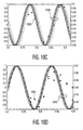
- FIGS. 10A - 10D shows swing curve predictions from each wafer cross-plotted with measured line width.
- the measured line width 1005 is plotted with swing curve predictions 1010.
- measured line width 1015 is plotted with swing curve predictions 1020.
- measured line width 1025 is plotted with swing curve predictions 1030.
- measured line width 1035 is plotted with swing curve predictions 1040. Note that each curve is an independent prediction of the relevant swing curve. Typically, predictions on the same substrate agreed within ⁇ 0.0045 ⁇ m.
- Table 5 summarizes prediction of local minimum and maximum compared to estimates based on line width measurements versus resist thickness.
- SPR660/Aquatar on PBL the predicted extrema bracket the measured value.
- the SPR660/Aquatar on PBL swing curve was relatively noisy so the agreement between predicted and the actual extrema may be significantly better than shown in FIG. 10D .
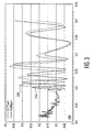
- IG. 11 shows the theoretical dependence of a swing curve for 0.35 ⁇ m lines and spaces for numerical apertures (1105) ranging from 0.3 to 0.9. However, the trend is quite apparent in that the swing curve amplitude decreases and peak shift increases relative to low numerical apertures.
- the methods for determining an optimal resist thickness according to the invention is applicable in the fabrication of state of the art semiconductor devices by substantially increasing accuracy of the determined minima and maxima of the swing curve while simultaneously limiting the number of wafers used to fewer than used with prior art methods. Therefore, the present invention provides a more accurate and less labor-intensive method for determining an optimal resist thickness. Table 5.
Landscapes
- Physics & Mathematics (AREA)
- General Physics & Mathematics (AREA)
- Exposure Of Semiconductors, Excluding Electron Or Ion Beam Exposure (AREA)
- Length Measuring Devices By Optical Means (AREA)
- Photosensitive Polymer And Photoresist Processing (AREA)
Claims (23)
- Verfahren (100) zur Bestimmung einer optimalen Resistdicke, umfassend die folgenden Schritte:a) Bereitstellen eines ersten Substrats (110), das unter Verwendung eines ersten Auftrageprogramms mit einem Resistfilm mit einer ersten Dicke überzogen wurde (105);b) Messen der ersten Dicke (115);c) Bereitstellen eines zweiten Substrats (120), das unter Verwendung des ersten Auftrageprogramms mit einem Resistfilm überzogen wurde;d) Einwirkenlassen einer Strahlung auf den Resistfilm auf dem zweiten Substrat und Messen eines Reflexionsspektrums nahe der aktinischen Wellenlänge des Resistfilms (140);e) Bestimmen eines effektiven Brechungsindexes (145) als eine Funktion der Periodizität des Reflexionsspektrums;f) Bestimmen einer Periodizität einer Schwingkurve (150) des auf das zweite Substrat aufgetragenen Resistfilms auf Basis des effektiven Brechungsindexes; undg) Bestimmen von Maxima und Minima (185) als eine Funktion der Periodizität.
- Verfahren nach Anspruch 1, ferner umfassend die folgenden Schritte:h) Wiederholen der Schritte a) bis g) unter Verwendung eines zweiten Auftrageprogramms (20) zur Bereitstellung eines Resistfilms mit einer zweiten Dicke; undi) Bestimmen von durchschnittlichen Maxima und Minima (185) als eine Funktion ihrer jeweiligen Periodizitäten.
- Verfahren nach Anspruch 2, wobei das erste Substrat ein einfaches Substrat umfasst.
- Verfahren nach Anspruch 3, wobei das erste Substrat Silizium umfasst.
- Verfahren nach Anspruch 2, wobei die erste Dicke so gewählt ist, dass sie nahe einer unteren Grenze eines vorbestimmten Bereichs für die optimale Resistdicke liegt.
- Verfahren nach Anspruch 5, wobei die zweite Dicke so gewählt ist, dass sie nahe einer oberen Grenze des vorbestimmten Bereichs für die optimale Resistdicke liegt.
- Verfahren nach Anspruch 6, wobei in Schritt e) die Periodizität des Reflexionsspektrums an cos(4πnEfft/λ) angepasst wird, wobei nEff der effektive Brechungsindex ist, t die Dicke des Resistfilms ist, und λ die Wellenlänge der Strahlung ist.
- Verfahren nach Anspruch 7, wobei die Strahlung UV-Strahlung umfasst.
- Verfahren nach Anspruch 1,
wobei die erste Dicke nahe einer unteren Grenze eines vorbestimmten Bereichs für die optimale Dicke liegt;
wobei der Resistfilm auf dem zweiten Substrat einer UV-Strahlung ausgesetzt wird;
wobei ein UV-Reflexionsspektrum nahe der aktinischen Wellenlänge des Resistfilms gemessen wird (140). - Verfahren nach Anspruch 9, ferner umfassend die folgenden Schritte:g) Wiederholen der Schritte a) bis f) unter Verwendung eines zweiten Auftrageprogramms (20), um einen Resistfilm mit einer zweiten Dicke bereitzustellen, wobei die zweite Dicke nahe einer oberen Grenze des vorbestimmten Bereichs für die optimale Dicke liegt; undh) Bestimmen durchschnittlicher Maxima und Minima als eine Funktion ihrer jeweiligen Periodizitäten (185).
- Verfahren nach Anspruch 10, wobei das erste Substrat ein einfaches Substrat umfasst.
- Verfahren nach Anspruch 11, wobei das erste Substrat Silizium umfasst.
- Verfahren nach Anspruch 10, wobei in Schritt e) die Periodizität des UV-Reflexionsspektrums an cos(4πnEfft/λ) angepasst wird, wobei nEff der effektive Brechungsindex ist, t die Dicke des Resistfilms ist, und λ die Wellenlänge der Strahlung ist.
- Verfahren nach Anspruch 1, umfassend:Bereitstellen von zwei Wafern, die das erste Substrat, das ein einfaches Substrat ist, umfassen;Bereitstellen von zwei Wafern, die das zweite Substrat umfassen;Überziehen der beiden Wafer, die das erste Substrat umfassen, mit Resistfilmen mit der ersten und einer zweiten Dicke nahe einer oberen bzw. einer unteren Grenze des vorbestimmten Bereichs für die optimale Resistdicke unter Verwendung des ersten und eines zweiten Auftrageprogramms (110, 165);Messen der ersten und der zweiten Dicke (115, 170);Überziehen der beiden Wafer, die das zweite Substrat umfassen, mit Resistfilmen unter Verwendung des ersten und des zweiten Auftrageprogramms (120, 175);Einwirkenlassen einer UV-Strahlung auf den Resistfilm auf den beiden Wafern, die das zweite Substrat umfassen, und Messen eines ersten und eines zweiten Reflexionsspektrums nahe der aktinischen Wellenlänge des Resistfilms (140);Anpassen von sinusförmigen Bestandteilen des ersten und des zweiten UV-Reflexionsspektrums;Bestimmen eines ersten und eines zweiten effektiven Brechungsindexes (145) bei der aktinischen Wellenlänge auf Basis der angepassten sinusförmigen Bestandteile des ersten und des zweiten UV-Reflexionsspektrums;Bestimmen von Minima und Maxima einer ersten und einer zweiten Schwingkurve unter Verwendung des ersten bzw. des zweiten effektiven Brechungsindexes; undBestimmen korrigierter Minima und Maxima durch Mitteln der Minima und Maxima der ersten und der zweiten Schwingkurve (185).
- Verfahren nach Anspruch 14, wobei das erste Substrat Silizium umfasst.
- Verfahren nach Anspruch 14, wobei die Periodizität des UV-Reflexionsspektrums an cos(4πnEfft/λ) angepasst wird, wobei nEff der effektive Brechungsindex ist, t die Dicke des Resistfilms ist, und λ die Wellenlänge der Strahlung ist.
- Verfahren nach Anspruch 16, wobei eine beste Anpassung durch Iterieren einer Cauchy-Entwicklung des effektiven Brechungsindexes gefunden wird.
- Verfahren nach Anspruch 17, wobei die korrigierten Minima und Maxima umgekehrt zu ihren relativen Abständen von den bestimmten Minima und Maxima gewichtet werden.
- Verfahren nach Anspruch 18, wobei der vorbestimmte Bereich zwischen 0,8 µm und 0,9 µm liegt.
- Verfahren (600) zur Bestimmung einer optimalen Dicke eines Resistfilms auf einem Wafersubstrat, umfassend die folgenden Schritte:Ablagern des Resistfilms (605, 610, 615, 620,625) mit einer vorbestimmten Dicke auf einem ersten Wafersubstrat;Einwirkenlassen einer Strahlung auf den Resistfilm und Messen eines Reflexionsspektrums (630) nahe der aktinischen Wellenlänge des Resistfilms, wobei das Reflexionsspektrum eine Periodizität aufweist; undVorhersagen der Periodizität einer Schwingkurve (635) aus der Periodizität des Reflexionsspektrums.
- Verfahren nach Anspruch 20, wobei die Periodizität der Schwingkurve eine Funktion des Einfallswinkels der Strahlung, der Phasenverschiebung von reflektierenden Grenzflächen im Wafersubstrat, und der Belichtungswellenlänge, und der Dicke des Resistfilms ist.
- Verfahren nach Anspruch 21, wobei die Phasenverschiebung von den reflektierenden Grenzflächen im Wafersubstrat von einer quadratischen Funktion der Wellenzahl regressiert wird, wobei δ = δ0 + δ1/λ + δ2/λ2 ist.
- Verfahren nach Anspruch 22, wobei die Wellenlänge vom Brechungsindex abhängt, wobei ein effektiver Brechungsindex durch eine Regression einer Cauchy-Entwicklung des effektiven Brechungsindex,

Applications Claiming Priority (3)
| Application Number | Priority Date | Filing Date | Title |
|---|---|---|---|
| US49369803P | 2003-08-08 | 2003-08-08 | |
| US51271703P | 2003-10-20 | 2003-10-20 | |
| PCT/IB2004/002546 WO2005015312A2 (en) | 2003-08-08 | 2004-08-07 | Method for determining optimal resist thickness |
Publications (2)
| Publication Number | Publication Date |
|---|---|
| EP1654591A2 EP1654591A2 (de) | 2006-05-10 |
| EP1654591B1 true EP1654591B1 (de) | 2008-05-14 |
Family
ID=34138761
Family Applications (1)
| Application Number | Title | Priority Date | Filing Date |
|---|---|---|---|
| EP04769111A Expired - Lifetime EP1654591B1 (de) | 2003-08-08 | 2004-08-07 | Verfahren zur bestimmung einer optimalen resistdicke |
Country Status (8)
| Country | Link |
|---|---|
| US (1) | US7492465B2 (de) |
| EP (1) | EP1654591B1 (de) |
| KR (1) | KR20060063942A (de) |
| CN (1) | CN100555080C (de) |
| AT (1) | ATE395632T1 (de) |
| DE (1) | DE602004013794D1 (de) |
| TW (1) | TW200512927A (de) |
| WO (1) | WO2005015312A2 (de) |
Families Citing this family (5)
| Publication number | Priority date | Publication date | Assignee | Title |
|---|---|---|---|---|
| US7171311B2 (en) | 2001-06-18 | 2007-01-30 | Rosetta Inpharmatics Llc | Methods of assigning treatment to breast cancer patients |
| DE602004018690D1 (de) | 2003-10-20 | 2009-02-05 | Nxp Bv | Verfahren zur bestimmung der relativen auslenkkurvenamplitude |
| US7582413B2 (en) * | 2005-09-26 | 2009-09-01 | Asml Netherlands B.V. | Substrate, method of exposing a substrate, machine readable medium |
| EP2899498B1 (de) * | 2014-01-28 | 2020-03-11 | ABB Schweiz AG | Sensorsystem und Verfahren zur Charakterisierung eines beschichteten Körpers |
| EP2899497B1 (de) * | 2014-01-28 | 2019-03-13 | ABB Schweiz AG | Sensorsystem und Verfahren zur Charakterisierung einer nassen Farbschicht |
Family Cites Families (6)
| Publication number | Priority date | Publication date | Assignee | Title |
|---|---|---|---|---|
| JP3714430B2 (ja) * | 1996-04-15 | 2005-11-09 | シャープ株式会社 | 分布帰還型半導体レーザ装置 |
| US5916717A (en) * | 1998-03-19 | 1999-06-29 | Industrial Technology Research Institute | Process utilizing relationship between reflectivity and resist thickness for inhibition of side effect caused by halftone phase shift masks |
| US6252670B1 (en) * | 1999-10-29 | 2001-06-26 | Taiwan Semiconductor Manufacturing Company | Method for accurately calibrating a constant-angle reflection-interference spectrometer (CARIS) for measuring photoresist thickness |
| CN1330287A (zh) * | 2000-06-21 | 2002-01-09 | 中国科学院光电技术研究所 | 衰减相移掩模及其制作方法 |
| JP2002277220A (ja) * | 2001-03-19 | 2002-09-25 | Hitachi Ltd | 膜厚計測のための計測点決定方法およびそれを用いた薄膜デバイスの製造方法並びに薄膜デバイスの製造装置 |
| KR100783603B1 (ko) * | 2002-01-05 | 2007-12-07 | 삼성전자주식회사 | 포토레지스트 조성물 및 이를 사용한 패턴의 형성방법 |
-
2004
- 2004-08-05 TW TW093123536A patent/TW200512927A/zh unknown
- 2004-08-07 EP EP04769111A patent/EP1654591B1/de not_active Expired - Lifetime
- 2004-08-07 US US10/568,653 patent/US7492465B2/en not_active Expired - Fee Related
- 2004-08-07 CN CNB2004800293384A patent/CN100555080C/zh not_active Expired - Fee Related
- 2004-08-07 WO PCT/IB2004/002546 patent/WO2005015312A2/en not_active Ceased
- 2004-08-07 KR KR1020067002743A patent/KR20060063942A/ko not_active Ceased
- 2004-08-07 AT AT04769111T patent/ATE395632T1/de not_active IP Right Cessation
- 2004-08-07 DE DE602004013794T patent/DE602004013794D1/de not_active Expired - Lifetime
Also Published As
| Publication number | Publication date |
|---|---|
| WO2005015312A2 (en) | 2005-02-17 |
| KR20060063942A (ko) | 2006-06-12 |
| ATE395632T1 (de) | 2008-05-15 |
| CN100555080C (zh) | 2009-10-28 |
| CN1864101A (zh) | 2006-11-15 |
| US7492465B2 (en) | 2009-02-17 |
| DE602004013794D1 (de) | 2008-06-26 |
| TW200512927A (en) | 2005-04-01 |
| WO2005015312A3 (en) | 2006-03-23 |
| EP1654591A2 (de) | 2006-05-10 |
| US20080206687A1 (en) | 2008-08-28 |
Similar Documents
| Publication | Publication Date | Title |
|---|---|---|
| US7042569B2 (en) | Overlay alignment metrology using diffraction gratings | |
| US6579733B1 (en) | Using scatterometry to measure resist thickness and control implant | |
| US6410421B1 (en) | Semiconductor device with anti-reflective structure and methods of manufacture | |
| Widmann et al. | Linewidth variations in photoresist patterns on profiled surfaces | |
| JP2867964B2 (ja) | レジスト膜パターンの形成方法 | |
| EP1654591B1 (de) | Verfahren zur bestimmung einer optimalen resistdicke | |
| Bencher et al. | Dielectric antireflective coatings for DUV lithography | |
| US6252670B1 (en) | Method for accurately calibrating a constant-angle reflection-interference spectrometer (CARIS) for measuring photoresist thickness | |
| US7642021B2 (en) | Method of mapping lithography focus errors | |
| JPH0423816B2 (de) | ||
| US7824827B2 (en) | Method and system for improved lithographic processing | |
| Ziger | Swing curve prediction from reflectance spectra: a new method to predict optimal resist thicknesses and compare processes | |
| JPH04239116A (ja) | 半導体装置の製造方法 | |
| JPH1131650A (ja) | 反射防止膜、被処理基板、被処理基板の製造方法、微細パターンの製造方法、および半導体装置の製造方法 | |
| EP1728122B1 (de) | Verfahren zur bestimmung der relativen auslenkkurvenamplitude | |
| Thane et al. | Lithographic effects of metal reflectivity variations | |
| Mack | Lithography on reflective substrates | |
| JPH0737799A (ja) | 半導体装置の微細パターン形成方法 | |
| Gu et al. | Single wafer process to generate reliable swing curves | |
| JPH0982596A (ja) | パターン形成方法 | |
| Lucas et al. | Antireflective coating optimization techniques for sub-0.2-um geometries | |
| Lyons et al. | Improved resist profiles and CD control through optimized thin dielectric stacks | |
| Tanaka et al. | A new method for reflectivity measurement at the interface between resist and substrate | |
| Saulnier et al. | Feasibility study of resist slimming for SIT | |
| JPH08148405A (ja) | 半導体装置の製造方法 |
Legal Events
| Date | Code | Title | Description |
|---|---|---|---|
| PUAI | Public reference made under article 153(3) epc to a published international application that has entered the european phase |
Free format text: ORIGINAL CODE: 0009012 |
|
| PUAK | Availability of information related to the publication of the international search report |
Free format text: ORIGINAL CODE: 0009015 |
|
| AK | Designated contracting states |
Kind code of ref document: A2 Designated state(s): AT BE BG CH CY CZ DE DK EE ES FI FR GB GR HU IE IT LI LU MC NL PL PT RO SE SI SK TR |
|
| AX | Request for extension of the european patent |
Extension state: AL HR LT LV MK |
|
| 17P | Request for examination filed |
Effective date: 20060925 |
|
| RBV | Designated contracting states (corrected) |
Designated state(s): AT BE BG CH CY CZ DE DK EE ES FI FR GB GR HU IE IT LI LU MC NL PL PT RO SE SI SK TR |
|
| DAX | Request for extension of the european patent (deleted) | ||
| 17Q | First examination report despatched |
Effective date: 20061124 |
|
| RAP1 | Party data changed (applicant data changed or rights of an application transferred) |
Owner name: NXP B.V. |
|
| GRAP | Despatch of communication of intention to grant a patent |
Free format text: ORIGINAL CODE: EPIDOSNIGR1 |
|
| GRAS | Grant fee paid |
Free format text: ORIGINAL CODE: EPIDOSNIGR3 |
|
| GRAA | (expected) grant |
Free format text: ORIGINAL CODE: 0009210 |
|
| AK | Designated contracting states |
Kind code of ref document: B1 Designated state(s): AT BE BG CH CY CZ DE DK EE ES FI FR GB GR HU IE IT LI LU MC NL PL PT RO SE SI SK TR |
|
| REG | Reference to a national code |
Ref country code: GB Ref legal event code: FG4D |
|
| REG | Reference to a national code |
Ref country code: CH Ref legal event code: EP |
|
| REG | Reference to a national code |
Ref country code: IE Ref legal event code: FG4D Free format text: LANGUAGE OF EP DOCUMENT: FRENCH |
|
| REF | Corresponds to: |
Ref document number: 602004013794 Country of ref document: DE Date of ref document: 20080626 Kind code of ref document: P |
|
| PG25 | Lapsed in a contracting state [announced via postgrant information from national office to epo] |
Ref country code: SI Free format text: LAPSE BECAUSE OF FAILURE TO SUBMIT A TRANSLATION OF THE DESCRIPTION OR TO PAY THE FEE WITHIN THE PRESCRIBED TIME-LIMIT Effective date: 20080514 |
|
| PG25 | Lapsed in a contracting state [announced via postgrant information from national office to epo] |
Ref country code: FI Free format text: LAPSE BECAUSE OF FAILURE TO SUBMIT A TRANSLATION OF THE DESCRIPTION OR TO PAY THE FEE WITHIN THE PRESCRIBED TIME-LIMIT Effective date: 20080514 Ref country code: ES Free format text: LAPSE BECAUSE OF FAILURE TO SUBMIT A TRANSLATION OF THE DESCRIPTION OR TO PAY THE FEE WITHIN THE PRESCRIBED TIME-LIMIT Effective date: 20080825 |
|
| NLV1 | Nl: lapsed or annulled due to failure to fulfill the requirements of art. 29p and 29m of the patents act | ||
| PG25 | Lapsed in a contracting state [announced via postgrant information from national office to epo] |
Ref country code: NL Free format text: LAPSE BECAUSE OF FAILURE TO SUBMIT A TRANSLATION OF THE DESCRIPTION OR TO PAY THE FEE WITHIN THE PRESCRIBED TIME-LIMIT Effective date: 20080514 Ref country code: AT Free format text: LAPSE BECAUSE OF FAILURE TO SUBMIT A TRANSLATION OF THE DESCRIPTION OR TO PAY THE FEE WITHIN THE PRESCRIBED TIME-LIMIT Effective date: 20080514 Ref country code: PL Free format text: LAPSE BECAUSE OF FAILURE TO SUBMIT A TRANSLATION OF THE DESCRIPTION OR TO PAY THE FEE WITHIN THE PRESCRIBED TIME-LIMIT Effective date: 20080514 |
|
| PG25 | Lapsed in a contracting state [announced via postgrant information from national office to epo] |
Ref country code: DK Free format text: LAPSE BECAUSE OF FAILURE TO SUBMIT A TRANSLATION OF THE DESCRIPTION OR TO PAY THE FEE WITHIN THE PRESCRIBED TIME-LIMIT Effective date: 20080514 Ref country code: CZ Free format text: LAPSE BECAUSE OF FAILURE TO SUBMIT A TRANSLATION OF THE DESCRIPTION OR TO PAY THE FEE WITHIN THE PRESCRIBED TIME-LIMIT Effective date: 20080514 Ref country code: PT Free format text: LAPSE BECAUSE OF FAILURE TO SUBMIT A TRANSLATION OF THE DESCRIPTION OR TO PAY THE FEE WITHIN THE PRESCRIBED TIME-LIMIT Effective date: 20081014 Ref country code: SE Free format text: LAPSE BECAUSE OF FAILURE TO SUBMIT A TRANSLATION OF THE DESCRIPTION OR TO PAY THE FEE WITHIN THE PRESCRIBED TIME-LIMIT Effective date: 20080814 |
|
| PG25 | Lapsed in a contracting state [announced via postgrant information from national office to epo] |
Ref country code: BE Free format text: LAPSE BECAUSE OF FAILURE TO SUBMIT A TRANSLATION OF THE DESCRIPTION OR TO PAY THE FEE WITHIN THE PRESCRIBED TIME-LIMIT Effective date: 20080514 Ref country code: RO Free format text: LAPSE BECAUSE OF FAILURE TO SUBMIT A TRANSLATION OF THE DESCRIPTION OR TO PAY THE FEE WITHIN THE PRESCRIBED TIME-LIMIT Effective date: 20080514 Ref country code: SK Free format text: LAPSE BECAUSE OF FAILURE TO SUBMIT A TRANSLATION OF THE DESCRIPTION OR TO PAY THE FEE WITHIN THE PRESCRIBED TIME-LIMIT Effective date: 20080514 |
|
| PLBE | No opposition filed within time limit |
Free format text: ORIGINAL CODE: 0009261 |
|
| STAA | Information on the status of an ep patent application or granted ep patent |
Free format text: STATUS: NO OPPOSITION FILED WITHIN TIME LIMIT |
|
| PG25 | Lapsed in a contracting state [announced via postgrant information from national office to epo] |
Ref country code: MC Free format text: LAPSE BECAUSE OF NON-PAYMENT OF DUE FEES Effective date: 20080831 |
|
| REG | Reference to a national code |
Ref country code: CH Ref legal event code: PL |
|
| 26N | No opposition filed |
Effective date: 20090217 |
|
| PG25 | Lapsed in a contracting state [announced via postgrant information from national office to epo] |
Ref country code: BG Free format text: LAPSE BECAUSE OF FAILURE TO SUBMIT A TRANSLATION OF THE DESCRIPTION OR TO PAY THE FEE WITHIN THE PRESCRIBED TIME-LIMIT Effective date: 20080814 Ref country code: EE Free format text: LAPSE BECAUSE OF FAILURE TO SUBMIT A TRANSLATION OF THE DESCRIPTION OR TO PAY THE FEE WITHIN THE PRESCRIBED TIME-LIMIT Effective date: 20080514 |
|
| PG25 | Lapsed in a contracting state [announced via postgrant information from national office to epo] |
Ref country code: CH Free format text: LAPSE BECAUSE OF NON-PAYMENT OF DUE FEES Effective date: 20080831 Ref country code: LI Free format text: LAPSE BECAUSE OF NON-PAYMENT OF DUE FEES Effective date: 20080831 |
|
| PG25 | Lapsed in a contracting state [announced via postgrant information from national office to epo] |
Ref country code: IE Free format text: LAPSE BECAUSE OF NON-PAYMENT OF DUE FEES Effective date: 20080807 |
|
| PG25 | Lapsed in a contracting state [announced via postgrant information from national office to epo] |
Ref country code: IT Free format text: LAPSE BECAUSE OF FAILURE TO SUBMIT A TRANSLATION OF THE DESCRIPTION OR TO PAY THE FEE WITHIN THE PRESCRIBED TIME-LIMIT Effective date: 20080514 |
|
| PG25 | Lapsed in a contracting state [announced via postgrant information from national office to epo] |
Ref country code: CY Free format text: LAPSE BECAUSE OF FAILURE TO SUBMIT A TRANSLATION OF THE DESCRIPTION OR TO PAY THE FEE WITHIN THE PRESCRIBED TIME-LIMIT Effective date: 20080514 Ref country code: LU Free format text: LAPSE BECAUSE OF NON-PAYMENT OF DUE FEES Effective date: 20080807 Ref country code: HU Free format text: LAPSE BECAUSE OF FAILURE TO SUBMIT A TRANSLATION OF THE DESCRIPTION OR TO PAY THE FEE WITHIN THE PRESCRIBED TIME-LIMIT Effective date: 20081115 |
|
| PG25 | Lapsed in a contracting state [announced via postgrant information from national office to epo] |
Ref country code: TR Free format text: LAPSE BECAUSE OF FAILURE TO SUBMIT A TRANSLATION OF THE DESCRIPTION OR TO PAY THE FEE WITHIN THE PRESCRIBED TIME-LIMIT Effective date: 20080514 |
|
| PG25 | Lapsed in a contracting state [announced via postgrant information from national office to epo] |
Ref country code: GR Free format text: LAPSE BECAUSE OF FAILURE TO SUBMIT A TRANSLATION OF THE DESCRIPTION OR TO PAY THE FEE WITHIN THE PRESCRIBED TIME-LIMIT Effective date: 20080815 |
|
| PGFP | Annual fee paid to national office [announced via postgrant information from national office to epo] |
Ref country code: GB Payment date: 20110728 Year of fee payment: 8 Ref country code: FR Payment date: 20110902 Year of fee payment: 8 Ref country code: DE Payment date: 20110803 Year of fee payment: 8 |
|
| GBPC | Gb: european patent ceased through non-payment of renewal fee |
Effective date: 20120807 |
|
| REG | Reference to a national code |
Ref country code: FR Ref legal event code: ST Effective date: 20130430 |
|
| PG25 | Lapsed in a contracting state [announced via postgrant information from national office to epo] |
Ref country code: GB Free format text: LAPSE BECAUSE OF NON-PAYMENT OF DUE FEES Effective date: 20120807 Ref country code: DE Free format text: LAPSE BECAUSE OF NON-PAYMENT OF DUE FEES Effective date: 20130301 |
|
| PG25 | Lapsed in a contracting state [announced via postgrant information from national office to epo] |
Ref country code: FR Free format text: LAPSE BECAUSE OF NON-PAYMENT OF DUE FEES Effective date: 20120831 |
|
| REG | Reference to a national code |
Ref country code: DE Ref legal event code: R119 Ref document number: 602004013794 Country of ref document: DE Effective date: 20130301 |