EP1653729A1 - Abbildungseinrichtung - Google Patents
Abbildungseinrichtung Download PDFInfo
- Publication number
- EP1653729A1 EP1653729A1 EP04771182A EP04771182A EP1653729A1 EP 1653729 A1 EP1653729 A1 EP 1653729A1 EP 04771182 A EP04771182 A EP 04771182A EP 04771182 A EP04771182 A EP 04771182A EP 1653729 A1 EP1653729 A1 EP 1653729A1
- Authority
- EP
- European Patent Office
- Prior art keywords
- image data
- pixels
- moving images
- still image
- imaging element
- Prior art date
- Legal status (The legal status is an assumption and is not a legal conclusion. Google has not performed a legal analysis and makes no representation as to the accuracy of the status listed.)
- Withdrawn
Links
- 238000003384 imaging method Methods 0.000 title claims abstract description 115
- 230000000750 progressive effect Effects 0.000 claims description 4
- 238000000034 method Methods 0.000 abstract description 16
- 230000008569 process Effects 0.000 abstract description 16
- 238000006243 chemical reaction Methods 0.000 description 11
- 238000010586 diagram Methods 0.000 description 8
- 238000007781 pre-processing Methods 0.000 description 8
- 238000001444 catalytic combustion detection Methods 0.000 description 2
- 239000011159 matrix material Substances 0.000 description 2
- 230000004044 response Effects 0.000 description 2
- 230000009977 dual effect Effects 0.000 description 1
- 238000001914 filtration Methods 0.000 description 1
- 230000006870 function Effects 0.000 description 1
- 239000004973 liquid crystal related substance Substances 0.000 description 1
- 230000007246 mechanism Effects 0.000 description 1
- 238000012986 modification Methods 0.000 description 1
- 230000004048 modification Effects 0.000 description 1
- 238000005070 sampling Methods 0.000 description 1
Images


Classifications
-
- H—ELECTRICITY
- H04—ELECTRIC COMMUNICATION TECHNIQUE
- H04N—PICTORIAL COMMUNICATION, e.g. TELEVISION
- H04N1/00—Scanning, transmission or reproduction of documents or the like, e.g. facsimile transmission; Details thereof
- H04N1/21—Intermediate information storage
- H04N1/2104—Intermediate information storage for one or a few pictures
- H04N1/2112—Intermediate information storage for one or a few pictures using still video cameras
- H04N1/212—Motion video recording combined with still video recording
-
- H—ELECTRICITY
- H04—ELECTRIC COMMUNICATION TECHNIQUE
- H04N—PICTORIAL COMMUNICATION, e.g. TELEVISION
- H04N23/00—Cameras or camera modules comprising electronic image sensors; Control thereof
- H04N23/60—Control of cameras or camera modules
- H04N23/667—Camera operation mode switching, e.g. between still and video, sport and normal or high- and low-resolution modes
-
- H—ELECTRICITY
- H04—ELECTRIC COMMUNICATION TECHNIQUE
- H04N—PICTORIAL COMMUNICATION, e.g. TELEVISION
- H04N23/00—Cameras or camera modules comprising electronic image sensors; Control thereof
- H04N23/60—Control of cameras or camera modules
- H04N23/63—Control of cameras or camera modules by using electronic viewfinders
-
- H—ELECTRICITY
- H04—ELECTRIC COMMUNICATION TECHNIQUE
- H04N—PICTORIAL COMMUNICATION, e.g. TELEVISION
- H04N25/00—Circuitry of solid-state image sensors [SSIS]; Control thereof
- H04N25/40—Extracting pixel data from image sensors by controlling scanning circuits, e.g. by modifying the number of pixels sampled or to be sampled
- H04N25/42—Extracting pixel data from image sensors by controlling scanning circuits, e.g. by modifying the number of pixels sampled or to be sampled by switching between different modes of operation using different resolutions or aspect ratios, e.g. switching between interlaced and non-interlaced mode
-
- H—ELECTRICITY
- H04—ELECTRIC COMMUNICATION TECHNIQUE
- H04N—PICTORIAL COMMUNICATION, e.g. TELEVISION
- H04N25/00—Circuitry of solid-state image sensors [SSIS]; Control thereof
- H04N25/40—Extracting pixel data from image sensors by controlling scanning circuits, e.g. by modifying the number of pixels sampled or to be sampled
- H04N25/44—Extracting pixel data from image sensors by controlling scanning circuits, e.g. by modifying the number of pixels sampled or to be sampled by partially reading an SSIS array
- H04N25/445—Extracting pixel data from image sensors by controlling scanning circuits, e.g. by modifying the number of pixels sampled or to be sampled by partially reading an SSIS array by skipping some contiguous pixels within the read portion of the array
-
- H—ELECTRICITY
- H04—ELECTRIC COMMUNICATION TECHNIQUE
- H04N—PICTORIAL COMMUNICATION, e.g. TELEVISION
- H04N5/00—Details of television systems
- H04N5/76—Television signal recording
- H04N5/765—Interface circuits between an apparatus for recording and another apparatus
- H04N5/77—Interface circuits between an apparatus for recording and another apparatus between a recording apparatus and a television camera
- H04N5/772—Interface circuits between an apparatus for recording and another apparatus between a recording apparatus and a television camera the recording apparatus and the television camera being placed in the same enclosure
-
- H—ELECTRICITY
- H04—ELECTRIC COMMUNICATION TECHNIQUE
- H04N—PICTORIAL COMMUNICATION, e.g. TELEVISION
- H04N9/00—Details of colour television systems
- H04N9/79—Processing of colour television signals in connection with recording
- H04N9/7921—Processing of colour television signals in connection with recording for more than one processing mode
-
- H—ELECTRICITY
- H04—ELECTRIC COMMUNICATION TECHNIQUE
- H04N—PICTORIAL COMMUNICATION, e.g. TELEVISION
- H04N2101/00—Still video cameras
Definitions
- the present invention relates to an imaging device that can pick up a still image while picking up moving images.
- imaging devices that can pick up a still image while picking up moving images have been proposed.
- These imaging devices are generally provided with a moving image processing portion for processing image data for moving images that is obtained by reading out signal charges accumulated in a solid-state imaging element such as a CCD (charge coupled device) imaging element, and a still image processing portion for processing image data for a still image that is obtained from signal charges in a similar manner. If a first button for giving an instruction to pick up moving images is pressed, the image data that has been processed by the moving image processing portion is sequentially recorded onto a recording medium. If a second button for giving an instruction to pick up a still image is also pressed while the first button is pressed, the image data that has been processed by the still image processing portion is also recorded onto the recording medium (see JP 2001-103361A, for example).
- Conventional imaging devices read out signal charges from all pixels in an imaging element while moving images are picked up, and record and display the moving images by performing a thinning process that reduces the number of pixels in the image data obtained by processing the read out signal charges, in order to improve the quality of a still image that is picked up while the moving images are picked up.
- the present invention resolves the above-mentioned problems, and provides an imaging device that can pick up a still image while picking up moving images, in which a high-quality still image can be picked up, and also in which moving images can be picked up at a high frame rate.
- An imaging device is provided with an imaging element driven in a thinning read-out mode for reading out signal charges from a subset of pixels, or in an all-pixels read-out mode for reading out signal charges from all pixels.
- the imaging device of the present invention processes and records a series of first image data that is obtained by reading out signal charges repeatedly from the subset of pixels and that constitutes the moving images, and processes and records a portion of the first image data as a still image when an instruction to pick up the still image is given while picking up the moving images.
- the imaging device of the present invention processes and records a series of second image data that is obtained by reading out signal charges repeatedly from all of the pixels and that constitutes the moving images after the number of pixels of the second image data is thinned, and processes and records a portion of the second image data as a still image without thinning when an instruction to pick up the still image is given while picking up the moving images.
- the imaging device of the present invention is provided with a moving image processing portion for processing the first image data without thinning when the imaging element is driven in the thinning read-out mode, and for processing the second image data after the number of pixels of the second image data has been thinned when the imaging element is driven in the all-pixels read-out mode, and a still image processing portion for receiving an input of the first or second image data for one frame that is to be recorded as a still image, and for processing the input first or second image data without thinning when an instruction to pick up the still image is given while picking up moving images.
- the imaging element is driven in the in the thinning read-out mode for reading out signal charges from a subset of pixels, or in the all-pixels read-out mode for reading out signal charges from all pixels in the case of picking up moving images.
- the imaging element is driven in the thinning read-out mode, a series of image data constituting the moving images can be obtained at a high frame rate, and thus moving images showing a smooth movement of a photographic subject can be picked up.
- image data that is to be recorded as a still image is processed and recorded without thinning, and thus a high-quality still image can be picked up while the moving images are picked up.
- the number of pixels of the series of image data constituting the moving images is preferably thinned to the same number of pixels of the image data obtained in the case where the imaging element is driven in the thinning read-out mode, but this process is not necessarily required.
- the imaging device of the present invention is provided with a moving image processing portion and a still image processing portion, and thus in the case where the imaging element is driven in either the thinning read-out mode or the all-pixels read-out mode, a still image can be picked up while moving images are picked up.
- image data is processed by the still image processing portion in parallel with processing of the image data by the moving image processing portion, and thus even when a still image is picked up while moving images are picked up, the pick-up of the moving images is not interrupted, and the frame rate of the moving images does not become non-uniform due to an interruption of the processing of the image data constituting the moving images.
- the frame rate of moving images becomes higher than that in conventional imaging devices when the imaging element is driven in the all-pixels read-out mode, and smoother moving images can be picked up.
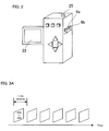
- FIG. 1 is a perspective view of an imaging device according to the present invention viewed from the front side.
- FIG. 1 is a perspective view of an imaging device according to an embodiment of the present invention viewed from the front side
- FIG. 2 is a perspective view of this imaging device viewed from the rear side.
- the imaging device is a digital video camera, and can pick up moving images.
- the front surface portion of the imaging device is provided with, for example, an imaging lens (1), and a moving image pick-up button (15) for starting an operation of picking up moving images.
- the imaging device operates in a moving image pick-up mode, it picks up moving images continuously while the moving image pick-up button (15) is pressed.
- the imaging device can pick up a still image while picking up moving images.
- the upper surface portion of the imaging device is provided with a release button (25) for starting an operation of picking up a still image. If the release button (25) is pressed in addition to the moving image pick-up button (15) while moving images are picked up, the imaging device also picks up a still image in parallel with the operation of picking up the moving images.
- One side surface portion of the imaging device is provided with an LCD (liquid crystal display) (22), serving as a display portion.
- the LCD (22) can display a so-called through-image, and serves as an EVF (electronic viewfinder).
- the other side surface portion and the rear surface portion of the imaging device are provided with various buttons and switches for operation.
- this side surface portion is provided with select buttons (6a) and (6b) for switching moving image pick-up modes.
- the moving image pick-up modes include two operation modes with different frame rates of the picked up moving images, that is, a first operation mode and a second operation mode. These modes are selected by pressing one of the select buttons (6a) and (6b).
- the select button (6a) When the select button (6a) is pressed, the first operation mode is selected, and moving images are picked up at a frame rate of 30 fps.
- the select button (6b) When the select button (6b) is pressed, the second operation mode is selected, and moving images are picked up at a frame rate of 15 fps.
- FIG. 3A is a diagram conceptually showing moving images that are picked up in the first operation mode
- FIG. 3B is a diagram conceptually showing moving images that are picked up in the second operation mode.
- the imaging device is provided with a CCD imaging element (2) (see FIG. 4).
- the CCD imaging element (2) is driven in a thinning read-out mode, signal charges are read out repeatedly from a subset of pixels in the CCD imaging element (2) at a cycle of 1/30 second, and moving images are picked up at a frame rate of 30 fps.
- the number of pixels (the degree of sharpness) of image data at each frame constituting the moving images is VGA size (640 ⁇ 480).
- the CCD imaging element (2) is driven in an all-pixels read-out mode, signal charges are read out repeatedly from all pixels (1600x1200) in the CCD imaging element (2) at a cycle of 1/15 second, and moving images are picked up at a frame rate of 15 fps.
- the number of pixels in the image data at each frame constituting the moving images is UXGA size (1600x1200).
- the first operation mode is selected in the case of picking up images showing a smooth movement, since signal charges are read out from a part of pixels in the CCD imaging element (2), and a series of image data constituting an image is created at a high frame rate.
- the second operation mode is selected in the case of picking up a high-quality still image while picking up moving images, since signal charges are read out from all pixels in the CCD imaging element (2), and image data of a large number of pixels (with a high degree of sharpness) is created.
- FIG. 4 is a block diagram showing a basic configuration of the imaging device of this embodiment.
- Light coming from a photographic subject is converged by the imaging lens (1), and is incident on the CCD imaging element (2), serving as an imaging element.
- This incident light is photoelectrically converted by photodiodes constituting the pixels in the CCD imaging element (2), and signal charges accumulated by this conversion are read out by driving a signal-charge transferring mechanism including a large number of vertical CCDs and one horizontal CCD (neither are shown).
- a CCD driven in progressive scan mode can read out signal charges from all pixels at a high speed.
- the imaging device of this embodiment drives the CCD imaging element (2) in the progressive scan mode, so that signal charges can be read out repeatedly from all pixels at a relatively short cycle (1/15 second) in the all-pixels read-out mode.
- the vertical CCDs and the horizontal CCD of the CCD imaging element (2) are driven respectively by vertical driving pulses and horizontal driving pulses that are sent from a timing generator (3).
- the timing generator (3) is provided with a VGA timing generator portion (3a) and an all-pixels timing generator portion (3b).
- the VGA timing generator portion (3a) generates vertical driving pulses and horizontal driving pulses in the thinning read-out mode so that signal charges are read out from pixels of about VGA size contained in the CCD imaging element (2) at a cycle of 1/30 second.
- the all-pixels timing generator portion (3b) generates vertical driving pulses and horizontal driving pulses in the all-pixels read-out mode so that signal charges are read out from all pixels contained in the CCD imaging element (2) at a cycle of 1/15 second.
- the CCD imaging element (2) is connected via a first switch (4) with the timing generator (3).
- the first switch (4) switches the driving pulses sent to the CCD imaging element (2) between the driving pulses from the VGA timing generator portion (3a) and the driving pulses from the all-pixels timing generator portion (3b).
- a CPU (5) switches the first switch (4) in accordance with the operation mode selected with the select buttons (6a) and (6b) (a line connecting the CPU (5) with the first switch (4) is not shown in FIG. 4, and this also the same for the other switches described below).
- the first switch (4) is set to the side of "a" shown in FIG. 4, and the driving pulses from the VGA timing generator portion (3a) are sent to the CCD imaging element (2).
- the CCD imaging element (2) is driven in the thinning read-out mode.
- the first switch (4) is set to the side of "b" shown in FIG. 4, and the driving pulses from the all-pixels timing generator portion (3b) are sent to the CCD imaging element (2). Thereafter, the CCD imaging element (2) is driven in the all-pixels read-out mode.
- the timing generator (3) is connected with a synchronizing signal generator (7).
- the synchronizing signal generator (7) is provided with a VGA synchronizing signal generating portion (7a) and an all-pixels synchronizing signal generating portion (7b).
- the former supplies the VGA timing generator portion (3a) with a vertical synchronizing signal VSYNC and a horizontal synchronizing signal HSYNC that are necessary to generate driving pulses.
- the latter supplies the all-pixels timing generator portion (3b) with the same.
- the vertical synchronizing signal VSYNC is a pulse signal whose cycle is the inverse number of the frame rate.
- the cycle of a vertical synchronizing signal VSYNC generated by the VGA timing generator portion (3a) is 1/30 second, and the cycle of a vertical synchronizing signal VSYNC generated by the all-pixels timing generator portion (3b) is 1/15 second.
- the VGA synchronizing signal generating portion (7a) and the all-pixels synchronizing signal generating portion (7b) start to supply a vertical synchronizing signal VSYNC and a horizontal synchronizing signal HSYNC.
- the read out signal charges are converted into voltages by the CCD imaging element (2), and are output in the form of an image signal.
- the image signal that has been output from the CCD imaging element (2) at the cycle of the vertical synchronizing signal VSYNC undergoes such processes as correlation dual sampling and automatic gain control by a CDS/AGC portion (8), and is digitized into image data for one frame by an A/D conversion portion (9).
- the image data is sent from the A/D conversion portion (9) to a moving image processing portion (10).
- the moving image processing portion (10) is provided with, for example, a preprocessing portion (11), a VGA moving image processing portion (12), and a moving image compressing portion (13).
- the image data that has been sent from the A/D conversion portion (9) is input directly, or via the preprocessing portion (11), to the VGA moving image processing portion (12).
- the input side of the VGA moving image processing portion (12) is provided with a second switch (14).
- the second switch (14) switches the input to the VGA moving image processing portion (12) between the image data output from the A/D conversion portion (9) and the image data output from the preprocessing portion (11).
- the CPU (5) switches the second switch (14) in accordance with the operation mode selected with the select buttons (6a) and (6b).
- the same number of pixels as for VGA size are read out from the CCD imaging element (2).
- the second switch (14) is set to the side of "a” shown in FIG. 4, and the image data that has been output from the A/D conversion portion (9) is directly input to the VGA moving image processing portion (12).
- all pixels are read out from the CCD imaging element (2), undergo a filtering process by the preprocessing portion (11), and are output in the form of image data in which the number of pixels is thinned to VGA size.
- the second switch (14) is set to the side of "b" shown in FIG. 4, and the image data that has been output from the preprocessing portion (11) is input to the VGA moving image processing portion (12).
- the VGA moving image processing portion (12) divides the input image data of VGA size into R signal data, G signal data, and B signal data, and further converts them into Y signal data, B-Y signal data, and R-Y signal data by a matrix process.
- the moving image compressing portion (13) compresses the image data that has been converted into these signal data in accordance with the MPEG (moving picture experts group)-2 standard, or the MPEG-4 standard. After the compressing process, the image data is transferred via a bus (16) and a memory controller (17), and is stored in a buffer memory (18).
- the bus (16) is connected with the CPU (5).
- the CPU (5) controls the memory controller (17) so that the image data is read out from the buffer memory (18) when necessary, and controls an interface portion (19) so that the series of image data constituting the moving images is recorded onto a recording medium (20).
- Examples of the buffer memory (18) include SDRAMs, and examples of the recording medium (20) include memory cards and DVD-RAMs.
- uncompressed image data is sequentially sent from the VGA moving image processing portion (12) to the buffer memory (18). This image data is transferred via the bus (16) and an LCD driver (21), and is sequentially displayed on the LCD (22).
- the LCD (22) serves as an EVF.
- the image data that has been output from the A/D conversion portion (9) is sent via a third switch (23) to a still image processing portion (24). If the release button (25) is pressed in addition to the moving image pick-up button (15), the CPU turns on the third switch (23) for a predetermined period, and image data for one frame is sent from the A/D conversion portion (9) not only to the moving image processing portion (10) but also to the still image processing portion (24). The image data that has been sent to the still image processing portion (24) is recorded in the form of a still image.
- the still image processing portion (24) processes the image data that is to be recorded in the form of a still image.
- the still image processing portion (24) is provided with, for example, a fourth switch (26), a VGA still image processing portion (27a), and an all-pixels still image processing portion (27b).
- the fourth switch (26) switches the portion to which the image data is input from the A/D conversion portion (9).
- the fourth switch (26) is set to the side of "a” shown in FIG. 4 in the first operation mode, and is set to the side of "b” in the second operation mode.
- the image data is sent to the VGA still image processing portion (27a) in the first operation mode, and is sent to the all-pixels still image processing portion (27b) in the second operation mode.
- the CPU (5) switches the fourth switch (26) in accordance with the operation mode selected with the select buttons (6a) and (6b).
- the VGA still image processing portion (27a) divides the image data of VGA size in the first operation mode into R signal data, G signal data, and B signal data, and further converts them into Y signal data, B-Y signal data, and R-Y signal data by a matrix process.
- the all-pixels still image processing portion (27b) converts the image data of all-pixels size in the second operation mode into Y signal data, B-Y signal data, and R-Y signal data in a similar manner.
- the image data that has been output from the VGA still image processing portion (27a) or the all-pixels still image processing portion (27b) is sent to a still image compressing portion (28).
- the input side of the still image compressing portion (28) is provided with a fifth switch (29).
- the fifth switch (29) switches the input to the still image compressing portion (28) between the image data output from the VGA still image processing portion (27a) and the image data output from the all-pixels still image processing portion (27b).
- the fifth switch (29) is set to the side of "a” shown in FIG. 4 in the first operation mode, and is set to the side of "b” in the second operation mode.
- the image data that has been output from the VGA still image processing portion (24) is input to the still image compressing portion (27).
- the image data that has been output from the all-pixels still image processing portion (27b) is input to the still image compressing portion (28).
- the CPU (5) switches the fifth switch (29) in accordance with the operation mode selected with the select buttons (6a) and (6b).
- the still image compressing portion (28) compresses the image data in accordance with the JPEG (joint photographic cording experts group) standard. After the compressing process, the image data is transferred via the bus (16) and the memory controller (17), and is temporarily stored in the buffer memory (18).
- the CPU (5) controls the memory controller (17) and the interface portion (19) so that the image data is read out from the buffer memory (18) and is recorded onto the recording medium (20).
- the bus (16) is connected to a RAM (30) for temporarily storing data generated in accordance with the processing by the CPU (5).
- the bus (16) is further connected to a ROM (31), and the ROM (31) stores, for example, a multitask OS and various control programs that are run by the CPU (5).
- the CPU (5) is connected to an operating portion (32) that has the various buttons and switches shown in FIGs. 1 and 2.
- the operating portion (32) includes the select buttons (6a) and (6b).
- FIG. 5 is a diagram showing a relationship between a vertical synchronizing signal VSYNC and operations of the imaging device performed in synchronization periods in the case of picking up a still image while picking up moving images.
- the cycle (synchronization period) of a vertical synchronizing signal VSYNC is 1/30 second in the first operation mode, and is 1/15 second in the second operation mode.
- the CCD imaging element (2) is exposed to light.
- pulses of the vertical synchronizing signal VSYNC are on, the signal charges are read out, and image data obtained from the read out signal charges is processed by the moving image processing portion (10) in the next synchronization period.
- image data is processed by the still image processing portion (24) in parallel with the processing of the image data by the moving image processing portion (10).
- the release button (25) is pressed at a time during a synchronization period T1 (indicated by the arrow in FIG. 5)
- the signal charges accumulated by exposure in the synchronization period T1 are read out in a synchronization period T2
- image data obtained from the read out signal charges is processed by the still image processing portion (24) in parallel with processing them by the moving image processing portion (10).
- the buffer memory (18) stores the image data constituting the moving images and the image data that is to be recorded in the form of a still image.
- the multitask OS that is stored in the ROM (31) and that is run by the CPU (5) records the image data constituting the moving images onto the recording medium (20), and simultaneously records the image data for the still image onto the recording medium (20). It should be noted that it is possible to record the image data that is to be recorded in the form of a still image onto the recording medium (20) after the image data constituting the moving images has been recorded onto the recording medium (20).
- the imaging device of this embodiment can also pick up only a still image. If the operating portion (32) is operated to select the still image pick-up mode, the CPU (5) sets the first switch (4), the second switch (14), the fourth switch (26), and the fifth switch (29) in a similar manner to that in the second operation mode.
- the CCD imaging element (2) operates in a similar manner to that in the above-described second operation mode, and the image data for the still image is recorded when the release button (25) is pressed.
- the series of image data that is sent to the moving image processing portion (10) is neither compressed nor recorded in the still image pick-up mode.
- This operation of the imaging device in the still image pick-up mode is merely one example, and it is also possible to pick up only a still image by a different operation from the above.
- the CPU (5) determines whether or not the moving image pick-up mode is selected (step S1). If the moving image pick-up mode is not selected, the imaging' device operates in the still image pick-up mode (or other operation mode) (step S2). If the moving image pick-up mode is selected, the CPU (5) determines which of the first operation mode and the second operation mode is selected with the select buttons (6a) and (6b) (step S3).
- step S3 If the first operation mode is selected in step S3, the CPU (5) sets the first switch (4), the second switch (14), the fourth switch (26), and the fifth switch (29) to the side of "a" shown in FIG. 4 (step S4).
- a reset signal is sent from the CPU (5) to the synchronizing signal generator (7), and the synchronizing signal generator (7) starts to supply a vertical synchronizing signal VSYNC and a horizontal synchronizing signal HSYNC.
- Driving pulses are sent from the VGA timing generator portion (3a) in response to the vertical synchronizing signal VSYNC and the horizontal synchronizing signal HSYNC that are sent from the VGA synchronizing signal generating portion (7a), and the CCD imaging element (2) starts to be driven in the thinning read ⁇ out mode (step S5).
- the read ⁇ out cycle of signal charges is 1/30 second, and image data of VGA size obtained repeatedly by reading out the CCD imaging element (2) is sequentially processed by the VGA image processing portion (12), is transferred via, for example, the buffer memory (18), and is displayed on the LCD (22) in the form of a through-image.
- the CPU (5) determines whether or not the moving image pick-up button (15) has been turned on (step S6). If the moving image pick-up button (15) is pressed, an instruction to compress the image data is given to the moving image compressing portion (13), and the image data that has been processed by the VGA image processing portion (12) and the moving image compressing portion (13) is transferred via, for example, the buffer memory (18) and is recorded onto the recording medium (20) (step S7).
- the frame rate of the series of image data that is recorded in the form of moving images is 30 fps.
- the CPU (5) determines whether or not the release button (25) has been turned on while moving images are picked up (step S8). If the release button (25) is pressed in addition to the moving image pick-up button (15), the CPU (5) turns on the third switch (23) (step S9), and image data obtained from signal charges that are read out from the CCD imaging element (2) after the release button (25) has been pressed is sent to the still image processing portion (24). The CPU (5) records the image data of VGA size processed by the still image processing portion (24) onto the recording medium (20) in the form of a still image (step S10).
- the moving images are picked up continuously in steps S8 to S10, and the image data is processed by the still image processing portion (24) in parallel with processing the image data by the moving image processing portion (10).
- the multitask OS that is run by the CPU (5) reads out and records the image data constituting the moving images from the buffer memory (18) onto the recording medium (20), and simultaneously reads out and records the image data for the still image from the buffer memory (18) onto the recording medium (20).
- the CPU (5) determines whether or not the moving image pick-up button (15) has been turned off (step S11), and ends the image pick-up operation when the moving image pick-up button (15) is released.
- step S3 If the second operation mode is selected in step S3, the CPU (5) sets the first switch (4), the second switch (14), the fourth switch (26), and the fifth switch (29) to the side of "b" shown in FIG. 4 (step S12).
- a reset signal is sent from the CPU (5) to the synchronizing signal generator (7), and the synchronizing signal generator (7) starts to supply a vertical synchronizing signal VSYNC and a horizontal synchronizing signal HSYNC.
- Driving pulses are sent from the all-pixels timing generator portion (3b) in response to the vertical synchronizing signal VSYNC and the horizontal synchronizing signal HSYNC that are sent from the all-pixels synchronizing signal generating portion (7b), and the CCD imaging element (2) starts to be driven in the all-pixels read-out mode (step S13).
- the read-out cycle of signal charges is 1/15 second.
- Image data of UXGA size obtained repeatedly by reading out the CCD imaging element (2) is thinned to VGA size by the preprocessing portion (11), is sequentially processed by the VGA image processing portion (12), is transferred via, for example, the buffer memory (18), and is displayed on the LCD (22) in the form of a through-image.
- the CPU (5) determines whether or not the moving image pick-up button (15) has been turned on (step S14). If the moving image pick-up button (15) is pressed, an instruction to compress the image data is given to the moving image compressing portion (13), and the image data that has been processed by the preprocessing portion (11), the VGA image processing portion (12), and the moving image compressing portion (13) is transferred via, for example, the buffer memory (18) and is recorded onto the recording medium (20) (step S 15).
- the frame rate of the series of image data that is recorded in the form of moving images is 15 fps.
- the number of pixels of the image data that is recorded is that of VGA size.
- the CPU (5) determines whether or not the release button (25) has been turned on while moving images are picked up (step S16). If the release button (25) is pressed in addition to the moving image pick-up button (15), the CPU (5) turns on the third switch (23) (step S17), and image data obtained from signal charges that are read out from all pixels of the CCD imaging element (2) after the release button (25) has been pressed is sent to the still image processing portion (24). The CPU (5) records the image data of UXGA size processed by the still image processing portion (24) onto the recording medium (20) in the form of a still image (step S18).
- the moving images are picked up continuously in steps S16 to S18 in a similar manner to that in steps S8 to S10, and the image data is processed by the still image processing portion (24) in parallel with processing the image data by the moving image processing portion (10).
- the CPU (5) records the image data constituting the moving images onto the recording medium (20), and simultaneously reads out and records the image data for the still image from the buffer memory (18) onto the recording medium (20).
- the CPU (5) determines whether or not the moving image pick-up button (15) has been turned off (step S19), and ends the image pick-up operation when the moving image pick-up button (15) is released.
- An imaging device of the present invention has been described referring to a digital video camera as the embodiment.
- the present invention may be applied widely to imaging devices that use an imaging element and that pick up a still image while picking up moving images, and also may be applied to, for example, a digital still camera including a function of picking up moving images.
- the present invention provides an imaging device that can pick up a still image while picking up moving images, in which a high-quality still image can be picked up, and also in which moving images can be picked up at a high frame rate.
Landscapes
- Engineering & Computer Science (AREA)
- Multimedia (AREA)
- Signal Processing (AREA)
- Studio Devices (AREA)
- Transforming Light Signals Into Electric Signals (AREA)
- Television Signal Processing For Recording (AREA)
Applications Claiming Priority (2)
| Application Number | Priority Date | Filing Date | Title |
|---|---|---|---|
| JP2003206666A JP3992659B2 (ja) | 2003-08-08 | 2003-08-08 | 撮像装置 |
| PCT/JP2004/011141 WO2005020566A1 (ja) | 2003-08-08 | 2004-08-04 | 撮像装置 |
Publications (2)
| Publication Number | Publication Date |
|---|---|
| EP1653729A1 true EP1653729A1 (de) | 2006-05-03 |
| EP1653729A4 EP1653729A4 (de) | 2008-03-12 |
Family
ID=34208951
Family Applications (1)
| Application Number | Title | Priority Date | Filing Date |
|---|---|---|---|
| EP04771182A Withdrawn EP1653729A4 (de) | 2003-08-08 | 2004-08-04 | Abbildungseinrichtung |
Country Status (6)
| Country | Link |
|---|---|
| US (1) | US7369683B2 (de) |
| EP (1) | EP1653729A4 (de) |
| JP (1) | JP3992659B2 (de) |
| KR (1) | KR100768639B1 (de) |
| CN (1) | CN100377573C (de) |
| WO (1) | WO2005020566A1 (de) |
Families Citing this family (19)
| Publication number | Priority date | Publication date | Assignee | Title |
|---|---|---|---|---|
| JP4140518B2 (ja) * | 2003-12-15 | 2008-08-27 | ソニー株式会社 | 情報処理装置および方法、並びにプログラム |
| KR100713404B1 (ko) * | 2005-03-24 | 2007-05-04 | 삼성전자주식회사 | 동영상 녹화 중 사진 촬영을 할 수 있는 장치 및 방법 |
| JP4802565B2 (ja) * | 2005-06-17 | 2011-10-26 | ソニー株式会社 | 画像処理装置および方法、記録媒体、並びにプログラム |
| WO2007010753A1 (ja) * | 2005-07-15 | 2007-01-25 | Matsushita Electric Industrial Co., Ltd. | 撮像データ処理装置、撮像データ処理方法および撮像素子 |
| JP4282645B2 (ja) | 2005-08-31 | 2009-06-24 | 株式会社東芝 | 撮像装置 |
| JP2007150439A (ja) | 2005-11-24 | 2007-06-14 | Sony Corp | 撮像装置、撮像方法、およびプログラム |
| JP2007318725A (ja) | 2006-04-27 | 2007-12-06 | Olympus Imaging Corp | カメラ、カメラの撮影制御方法、プログラム、記録媒体 |
| KR100725186B1 (ko) | 2006-07-27 | 2007-06-04 | 삼성전자주식회사 | 이동통신 단말기의 화상 촬영 방법 및 그 장치 |
| JP4775648B2 (ja) * | 2006-08-16 | 2011-09-21 | ソニー株式会社 | 撮像装置、制御方法、およびプログラム |
| JP5171398B2 (ja) * | 2008-06-02 | 2013-03-27 | 三洋電機株式会社 | 撮像装置 |
| JP5230381B2 (ja) * | 2008-11-28 | 2013-07-10 | 三星電子株式会社 | 撮像装置及び撮像装置の制御方法 |
| US8502878B2 (en) | 2008-12-12 | 2013-08-06 | Olympus Imaging Corp. | Imaging apparatus having a changeable operating mode responsive to an inclined orientation |
| JP2010199927A (ja) * | 2009-02-25 | 2010-09-09 | Nikon Corp | 撮像装置 |
| JP5259464B2 (ja) | 2009-03-13 | 2013-08-07 | オリンパスイメージング株式会社 | 撮像装置およびそのモード切換え方法 |
| JP4983961B2 (ja) * | 2010-05-25 | 2012-07-25 | 株式会社ニコン | 撮像装置 |
| JP2012175303A (ja) * | 2011-02-18 | 2012-09-10 | Jvc Kenwood Corp | 撮像装置、撮像方法、及びプログラム |
| JP6306845B2 (ja) | 2013-09-12 | 2018-04-04 | キヤノン株式会社 | 撮像装置及びその制御方法 |
| JP6642991B2 (ja) * | 2015-07-14 | 2020-02-12 | キヤノン株式会社 | 画像処理装置、撮像装置および撮像制御プログラム |
| US10313594B2 (en) | 2017-01-05 | 2019-06-04 | Qualcomm Incorporated | Dynamically configuring memory bandwidth for image generation |
Citations (3)
| Publication number | Priority date | Publication date | Assignee | Title |
|---|---|---|---|---|
| EP1107567A2 (de) * | 1999-12-01 | 2001-06-13 | Sanyo Electric Co., Ltd. | Digitale Kamera |
| US20020024602A1 (en) * | 1996-09-25 | 2002-02-28 | Nikon Corporation | Electronic camera |
| US20030112340A1 (en) * | 1999-12-24 | 2003-06-19 | Shigeyuki Okada | Digital camera, memory control device usable for it, image processing device and image processing method |
Family Cites Families (10)
| Publication number | Priority date | Publication date | Assignee | Title |
|---|---|---|---|---|
| US5734424A (en) * | 1990-08-08 | 1998-03-31 | Canon Kabushiki Kaisha | Image pickup apparatus capable of providing moving video signal and still video signal |
| JPH1079910A (ja) * | 1996-09-05 | 1998-03-24 | Sony Corp | Vtr一体型カメラ装置 |
| JP3893424B2 (ja) * | 1998-11-06 | 2007-03-14 | 富士フイルム株式会社 | 固体撮像装置および信号読出し方法 |
| JP3980782B2 (ja) * | 1999-02-03 | 2007-09-26 | 富士フイルム株式会社 | 撮像制御装置および撮像制御方法 |
| JP2000261817A (ja) * | 1999-03-08 | 2000-09-22 | Hitachi Ltd | 撮像装置 |
| JP4309524B2 (ja) | 1999-09-27 | 2009-08-05 | オリンパス株式会社 | 電子カメラ装置 |
| JP2001238134A (ja) * | 2000-02-23 | 2001-08-31 | Sony Corp | 固体撮像素子およびその駆動方法並びにカメラシステム |
| JP3876973B2 (ja) * | 2001-10-15 | 2007-02-07 | 富士フイルムホールディングス株式会社 | 画像の記録再生方法、画像再生装置、並びにファイル管理方法及び装置 |
| JP3973408B2 (ja) * | 2001-11-22 | 2007-09-12 | 富士フイルム株式会社 | ディジタル・ムービ・カメラおよびその動作制御方法 |
| US6992707B2 (en) * | 2002-03-06 | 2006-01-31 | Hewlett-Packard Development Company, L.P. | Delayed encoding based joint video and still image pipeline with still burst mode |
-
2003
- 2003-08-08 JP JP2003206666A patent/JP3992659B2/ja not_active Expired - Fee Related
-
2004
- 2004-08-04 KR KR1020057022455A patent/KR100768639B1/ko not_active IP Right Cessation
- 2004-08-04 CN CNB2004800162424A patent/CN100377573C/zh not_active Expired - Fee Related
- 2004-08-04 US US10/538,872 patent/US7369683B2/en not_active Expired - Fee Related
- 2004-08-04 EP EP04771182A patent/EP1653729A4/de not_active Withdrawn
- 2004-08-04 WO PCT/JP2004/011141 patent/WO2005020566A1/ja active Application Filing
Patent Citations (3)
| Publication number | Priority date | Publication date | Assignee | Title |
|---|---|---|---|---|
| US20020024602A1 (en) * | 1996-09-25 | 2002-02-28 | Nikon Corporation | Electronic camera |
| EP1107567A2 (de) * | 1999-12-01 | 2001-06-13 | Sanyo Electric Co., Ltd. | Digitale Kamera |
| US20030112340A1 (en) * | 1999-12-24 | 2003-06-19 | Shigeyuki Okada | Digital camera, memory control device usable for it, image processing device and image processing method |
Non-Patent Citations (1)
| Title |
|---|
| See also references of WO2005020566A1 * |
Also Published As
| Publication number | Publication date |
|---|---|
| US20060050154A1 (en) | 2006-03-09 |
| CN1806431A (zh) | 2006-07-19 |
| CN100377573C (zh) | 2008-03-26 |
| US7369683B2 (en) | 2008-05-06 |
| EP1653729A4 (de) | 2008-03-12 |
| JP3992659B2 (ja) | 2007-10-17 |
| WO2005020566A1 (ja) | 2005-03-03 |
| KR20060038931A (ko) | 2006-05-04 |
| JP2005057378A (ja) | 2005-03-03 |
| KR100768639B1 (ko) | 2007-10-18 |
Similar Documents
| Publication | Publication Date | Title |
|---|---|---|
| US7369683B2 (en) | Imaging device | |
| US6963374B2 (en) | Method for live view display and digital camera using same | |
| US6784941B1 (en) | Digital camera with video input | |
| JP3973408B2 (ja) | ディジタル・ムービ・カメラおよびその動作制御方法 | |
| JP2003158653A5 (de) | ||
| JP2003244529A (ja) | デジタルカメラ | |
| JP5002931B2 (ja) | 撮像装置及びそのプログラム | |
| EP2534827B1 (de) | Bildaufnahmevorrichtung und steuerungsverfahren dafür | |
| JP2002101329A (ja) | デジタルカメラ、画像再生装置及び方法 | |
| EP1107567B1 (de) | Digitale Kamera | |
| EP1091572A2 (de) | Bildaufnahmevorrichtung mit einer Funktion zur Regelung der einfallenden Lichtmenge | |
| US9154758B2 (en) | Digital signal processor and digital image processing apparatus adopting the same with concurrent live view frame and picture image processing | |
| JP4245782B2 (ja) | 撮像装置 | |
| US7671896B2 (en) | Image sensing apparatus | |
| US7433099B2 (en) | Image sensing apparatus, image sensing method, program, and storage medium | |
| JP2002209125A (ja) | デジタルカメラ | |
| WO2011010747A1 (en) | Imaging apparatus and imaging method | |
| JP2003134386A (ja) | 撮像装置および撮像方法 | |
| JP2000041192A (ja) | 撮像装置及び撮像方法 | |
| JP5625325B2 (ja) | 画像データ記録装置および画像データ記録プログラム | |
| JPH11177866A (ja) | 撮像装置 | |
| JP4054918B2 (ja) | 撮像装置、撮影制御方法及び撮影制御プログラム | |
| JPH09163294A (ja) | ディジタルスチルカメラ | |
| JP5600935B2 (ja) | 画像記録装置、画像記録方法及び画像記録プログラム | |
| JP4064256B2 (ja) | 撮像装置および撮像方法 |
Legal Events
| Date | Code | Title | Description |
|---|---|---|---|
| PUAI | Public reference made under article 153(3) epc to a published international application that has entered the european phase |
Free format text: ORIGINAL CODE: 0009012 |
|
| 17P | Request for examination filed |
Effective date: 20050624 |
|
| AK | Designated contracting states |
Kind code of ref document: A1 Designated state(s): DE FR GB |
|
| DAX | Request for extension of the european patent (deleted) | ||
| RBV | Designated contracting states (corrected) |
Designated state(s): DE FR GB |
|
| A4 | Supplementary search report drawn up and despatched |
Effective date: 20080207 |
|
| 17Q | First examination report despatched |
Effective date: 20080729 |
|
| GRAP | Despatch of communication of intention to grant a patent |
Free format text: ORIGINAL CODE: EPIDOSNIGR1 |
|
| INTG | Intention to grant announced |
Effective date: 20130408 |
|
| STAA | Information on the status of an ep patent application or granted ep patent |
Free format text: STATUS: THE APPLICATION HAS BEEN WITHDRAWN |
|
| 18W | Application withdrawn |
Effective date: 20130612 |