EP1650737A1 - Verzögerungszeit-korrekturschaltung, videodatenverarbeitungsschaltung und flach-display-vorrichtung - Google Patents
Verzögerungszeit-korrekturschaltung, videodatenverarbeitungsschaltung und flach-display-vorrichtung Download PDFInfo
- Publication number
- EP1650737A1 EP1650737A1 EP04748180A EP04748180A EP1650737A1 EP 1650737 A1 EP1650737 A1 EP 1650737A1 EP 04748180 A EP04748180 A EP 04748180A EP 04748180 A EP04748180 A EP 04748180A EP 1650737 A1 EP1650737 A1 EP 1650737A1
- Authority
- EP
- European Patent Office
- Prior art keywords
- data
- logical level
- delay time
- period
- circuit
- Prior art date
- Legal status (The legal status is an assumption and is not a legal conclusion. Google has not performed a legal analysis and makes no representation as to the accuracy of the status listed.)
- Withdrawn
Links
Images


Classifications
-
- G—PHYSICS
- G09—EDUCATION; CRYPTOGRAPHY; DISPLAY; ADVERTISING; SEALS
- G09G—ARRANGEMENTS OR CIRCUITS FOR CONTROL OF INDICATING DEVICES USING STATIC MEANS TO PRESENT VARIABLE INFORMATION
- G09G3/00—Control arrangements or circuits, of interest only in connection with visual indicators other than cathode-ray tubes
- G09G3/20—Control arrangements or circuits, of interest only in connection with visual indicators other than cathode-ray tubes for presentation of an assembly of a number of characters, e.g. a page, by composing the assembly by combination of individual elements arranged in a matrix no fixed position being assigned to or needed to be assigned to the individual characters or partial characters
- G09G3/34—Control arrangements or circuits, of interest only in connection with visual indicators other than cathode-ray tubes for presentation of an assembly of a number of characters, e.g. a page, by composing the assembly by combination of individual elements arranged in a matrix no fixed position being assigned to or needed to be assigned to the individual characters or partial characters by control of light from an independent source
- G09G3/36—Control arrangements or circuits, of interest only in connection with visual indicators other than cathode-ray tubes for presentation of an assembly of a number of characters, e.g. a page, by composing the assembly by combination of individual elements arranged in a matrix no fixed position being assigned to or needed to be assigned to the individual characters or partial characters by control of light from an independent source using liquid crystals
- G09G3/3611—Control of matrices with row and column drivers
- G09G3/3685—Details of drivers for data electrodes
-
- G—PHYSICS
- G09—EDUCATION; CRYPTOGRAPHY; DISPLAY; ADVERTISING; SEALS
- G09G—ARRANGEMENTS OR CIRCUITS FOR CONTROL OF INDICATING DEVICES USING STATIC MEANS TO PRESENT VARIABLE INFORMATION
- G09G3/00—Control arrangements or circuits, of interest only in connection with visual indicators other than cathode-ray tubes
- G09G3/20—Control arrangements or circuits, of interest only in connection with visual indicators other than cathode-ray tubes for presentation of an assembly of a number of characters, e.g. a page, by composing the assembly by combination of individual elements arranged in a matrix no fixed position being assigned to or needed to be assigned to the individual characters or partial characters
- G09G3/34—Control arrangements or circuits, of interest only in connection with visual indicators other than cathode-ray tubes for presentation of an assembly of a number of characters, e.g. a page, by composing the assembly by combination of individual elements arranged in a matrix no fixed position being assigned to or needed to be assigned to the individual characters or partial characters by control of light from an independent source
- G09G3/36—Control arrangements or circuits, of interest only in connection with visual indicators other than cathode-ray tubes for presentation of an assembly of a number of characters, e.g. a page, by composing the assembly by combination of individual elements arranged in a matrix no fixed position being assigned to or needed to be assigned to the individual characters or partial characters by control of light from an independent source using liquid crystals
-
- G—PHYSICS
- G09—EDUCATION; CRYPTOGRAPHY; DISPLAY; ADVERTISING; SEALS
- G09G—ARRANGEMENTS OR CIRCUITS FOR CONTROL OF INDICATING DEVICES USING STATIC MEANS TO PRESENT VARIABLE INFORMATION
- G09G2300/00—Aspects of the constitution of display devices
- G09G2300/04—Structural and physical details of display devices
- G09G2300/0404—Matrix technologies
- G09G2300/0408—Integration of the drivers onto the display substrate
Definitions
- the present invention relates to a delay time correction circuit, a video data processing circuit, and a flat display device, and can be applied to, for example, a liquid crystal display device having a driving circuit integrally formed on an insulating substrate.
- the present invention makes it possible to effectively avoid a variation in delay time in a logical circuit using TFTs or the like by inserting dummy data into input data and forcedly switching the logical level of the input data.
- liquid crystal display device of the type in which a driving circuit for a liquid crystal display panel is integrally integrated and configured on a glass substrate which is an insulating substrate constituting part of the liquid crystal display panel has been provided as a liquid crystal display device which is a flat display device applied to mobile terminals such as mobile phones and PDAs.
- this kind of liquid crystal display device has a display section formed by pixels which are arranged in a matrix form and each of which is made of a liquid crystal cell, a low-temperature polysilicon TFT (Thin Film Transistor) which is a switching device for the liquid crystal cell, and a storage capacitor, and is configured to display various images by driving the display section by means of various driving circuits arranged at the periphery of the display section.
- a display section formed by pixels which are arranged in a matrix form and each of which is made of a liquid crystal cell, a low-temperature polysilicon TFT (Thin Film Transistor) which is a switching device for the liquid crystal cell, and a storage capacitor, and is configured to display various images by driving the display section by means of various driving circuits arranged at the periphery of the display section.
- TFT Thin Film Transistor
- Such a liquid crystal display device is configured so as to separate gradation data indicative of gradation of each pixel, which is sequentially inputted in raster scan order, for example, into gradation data for odd lines and even lines and drive the display section based on these gradation data for odd lines and even lines by means of horizontal driving circuits for odd lines and even lines which are respectively provided above and below the display section, so that wiring patterns in the display section are efficiently laid out and the pixels are arranged in fine pattern.
- This kind of logical circuit using low-temperature polysilicon TFTs which is applied to the liquid crystal display device has the problem that if an input value is held at an L level for a long time, delay time becomes long in response at the rise of the following logical level, so that the delay time varies according to the length of the immediately preceding logical level.
- a delay time tD is approximately constant.
- the liquid crystal display device In the case where data cannot be correctly latched, in the liquid crystal display device, if the gradation data is separated into even lines and odd lines so as to drive the display section of high resolution as above mentioned, pixels will be driven with locally erroneous gradations immediately after vertical blanking periods. In addition, if, for example, a white area having a window-like shape is to be displayed in a black background, a pixel will be similarly driven with an erroneous gradation at the start of scan of the white area.
- the gradation data D1 is inputted, for example, in a 6-bit parallel form corresponding to the number of gradation levels of the display section, so that a variation in delay time occurs in each bit of the gradation data. Accordingly, there occurs a case where erroneous data may be latched as to only a particular bit of the gradation data, so that an image to be displayed may become visually remarkably undesirable.
- the present invention has been made in view of the above-mentioned circumstances, and intends to propose a delay time correction circuit capable of effectively avoiding a variation in delay time in a logical circuit using TFTs or the like, a video data processing circuit using the delay time correction circuit, and a flat display device using the same.
- the present invention is applied to a delay time correction circuit for a data processing circuit for processing input data having a quiescent period during which the input data is held at a constant logical level for a constant period at a constant cycle, and in the delay time correction circuit, dummy data having a logical level opposite to the constant logical level is inserted into the input data at a predetermined timing during the quiescent period.
- the present invention if the present invention is applied to a delay time correction circuit for a data processing circuit for processing input data having a quiescent period during which the input data is held at a constant logical level for a constant period at a constant cycle, and in the delay time correction circuit, dummy data having a logical level opposite to the constant logical level is inserted into the input data at a predetermined timing during the quiescent period, the delay time of a variation in the following logical level can be made short compared to the case where dummy data is not at all inserted, so that a variation in delay time can be effectively avoided in the logical circuit using TFTs or the like.
- the present invention is applied to a data processing circuit for processing input data having a quiescent period during which the input data is held at a constant logical level for a constant period at a constant cycle, and in the data processing circuit, dummy data having a logical level opposite to the constant logical level is inserted into the input data at a predetermined timing during the quiescent period.
- the configuration of the present invention it is possible to effectively avoid a variation in delay time in the logical circuit using TFTs or the like, so that it is possible to perform data processing while effectively avoiding various influences due to the variation in delay time.
- the present invention is applied to a flat display device so that gradation data is processed by inserting dummy data having a logical level opposite to a logical level during a horizontal blanking period into the gradation data at a predetermined timing during the horizontal blanking period of the gradation data.
- the configuration of the present invention it is possible to effectively avoid a variation in delay time in the logical circuit using TFTs or the like, so that it is possible to display a desired image while effectively avoiding various influences due to the variation in delay time.
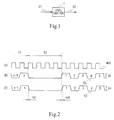
- Fig. 4 is a block diagram used in explaining a delay time correction principle according to the present invention by contrast with Fig. 1.
- dummy data having a logical level opposite to the constant logical level is inserted into the input data at a predetermined timing during a period in which the input level is held at the constant logical level.
- the period in which the input data is held at the constant logical level for the constant period at the constant period is a period in which transmission of significant data is not performed, such as a horizontal blanking period in video data.
- the period will be hereinafter referred to as the quiescent period as needed.
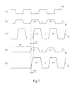
- the data processing circuit is, for example, a level shifter 1 which, as shown in Fig. 5, corrects input data D1 synchronized with a main clock MCK (Fig. 5(A)) from an amplitude of 0 to 3 (V) to an amplitude of 0 to 6 (V) and outputs output data D2 (Figs. 5(B) and 5(D)), dummy data DD which rises from a logical L level is inserted into the gradation data D1 during a horizontal blanking period T2 in which the gradation data D1 is held at a constant logical level for a constant period at a constant cycle. Accordingly, a reset pulse HDrst based on the dummy data DD is inserted into the gradation data D1 via, for example, an OR circuit 4 (Fig 5(C)).
- a delay time dt1 at the rise of the logical level immediately after the horizontal blanking period T is made short compared to the case where the dummy data DD is not at all inserted, thereby solving the problem that delay time varies according to the length of the immediately preceding logical level. More specifically, if the dummy data DD is inserted in this manner, the logical level of the input data is forcedly switched and the period during which the logical level of the input data is held at a logical L level can be made short compared to the case where the dummy data DD is not at all inserted, so that a variation in delay time can be reduced in a data string of the input data D1. Accordingly, it is possible to effectively avoid latching of erroneous data and the like.
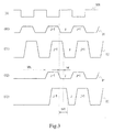
- the dummy data DD is inserted during horizontal blanking periods in a vertical blanking period VBL, so that the delay time of the output data D2 can be made short at the rise of the logical level following the vertical blanking period VBL and the output data D2 can be sampled and latched at a timing similar to the case of an active video period (Figs. 6(B1) to 6(C2)). Accordingly, it is possible to display a pixel corresponding to the rise of the vertical blanking period VBL with correct gradation.
- a liquid crystal display device can be adapted to correctly display the gradation of each pixel.
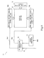
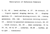
- Fig. 8 is a block diagram showing a liquid crystal display device according to Embodiment 1 of the present invention.
- the driving circuits shown in Fig. 8 are integrally formed on a glass substrate which is an insulating substrate of a display section 12, and driving circuits which will be described later, such as horizontal driving circuits and a timing generator, are formed by TFTs made of low-temperature polysilicon.
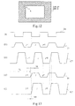
- the display section 12 has pixels each formed by a liquid crystal cell, a TFT which is a switching device for the liquid crystal cell, and a storage capacitor, and has a rectangular shape in which these pixels are arranged in a matrix form.
- a vertical driving circuit 13 drives gate lines of the display section 12 in response to various timing signals outputted from a timing generator 14, thereby sequentially selecting the pixels provided in the display section 12, in units of lines.
- Horizontal driving circuits 150 and 15E are provided above and below the display section 12, respectively, and after having sequentially cyclically latched gradation data Dod and Dev for odd lines and even lines, outputted from a serial-to-parallel (SP) conversion circuit 16, perform digital-to-analog conversion on the respective latch outputs and drive the corresponding ones of signal lines of the display section 12 by using the resultant driving signals.
- SP serial-to-parallel
- the horizontal driving circuits 150 and 15E respectively drives odd signal lines and even signal lines of the display section 12 and set each of the pixels selected by the vertical driving circuit 13 to a gradation based on the gradation data Dod and Dev.
- the timing generator 14 generates and outputs the various timing signals necessary for the operation of the liquid crystal display device 11 from various reference signals supplied from a device superior to the liquid crystal display device 11.
- the serial-to-parallel conversion circuit 16 separates the gradation data D1 outputted from the device superior to the liquid crystal display device 11 into the gradation data Dod and Dev for odd lines and even lines, and outputs the gradation data Dod and Dev.
- the gradation data D1 is data indicative of gradation for each pixel, and is formed by video data made of a continuation of red, blue and green data in raster scan order corresponding to the arrangement of the pixels of the display section 12.
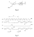
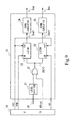
- Fig. 9 is a block diagram showing the serial-to-parallel conversion circuit 16 and a configuration associated therewith.
- the serial-to-parallel conversion circuit 16 converts the amplitude of the gradation data D1 ranging from 0 to 3 (V) into an amplitude of 0 to 6 (V) by means of a level shifter 21, causes latch circuits 22 and 23 to alternately latch the obtained gradation data D1 to separate the gradation data D1 into the gradation data Dod and Dev for odd lines and even lines, restore the original amplitude by means of down converters 24 and 25, and outputs the resultant gradation data Dod and Dev.
- the serial-to-parallel conversion circuit 16 enlarges and processes the amplitude of the gradation data D1 through level shifting by the level shifter 21 so as to reliably separate the gradation data D1 supplied at a high transfer rate into gradation data for two systems.
- the serial-to-parallel conversion circuit 16 has an OR circuit 27 provided at the output stage of the level shifter 21, and dummy data DD is inserted into the gradation data D1 during the horizontal blanking period of the gradation data D1 by the OR circuit 27. Accordingly, the liquid crystal display device 11 is adapted to prevent a variation in delay time due to the fact that the gradation data D1 is held at an L level for a long time, so that the gradation data D1 can be correctly latched in the following latch circuits 22 and 23.
- the liquid crystal display device 11 is configured to insert the dummy data DD at the output stage of the level shifter 21 in this manner, because the gradation data D1 is not erroneously latched due to only a variation in delay time occurring in the level shifter 21.
- the timing generator (TG) 14 is configured to output and supply to the OR circuit 27 a reset pulse HDrst by which signal level is risen during each horizontal blanking period.
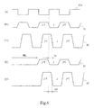
- Fig. 10 is a connection diagram showing the latch circuit 22.
- the latch circuits 22 and 23 are identically configured except that sampling pulses sp and xsp for controlling their latch timings are respectively supplied from the timing generator 14.
- sampling pulses sp and xsp for controlling their latch timings are respectively supplied from the timing generator 14.
- a reset pulse rst is shown, but the description thereof is omitted.
- the sampling pulse sp is inputted to an inverter 31, so that an inverted signal of the sampling pulse sp is generated.
- the gradation data D1 is inputted to an inverter 32 which is connected to positive and negative power sources VDD and VSS, respectively, by a P-channel MOS transistor Q1 which switches to an ON state in response to the sampling pulse sp and an N-channel MOS transistor Q2 which switches to an ON state in response to the inverted signal of the latch pulse sp outputted from the inverter 31.
- the output of the inverter 32 is connected to the output of an inverter 33 which is connected to the positive and negative power sources VDD and VSS, respectively, by a P-channel MOS transistor Q3 which switches to an ON state in response to the inverted signal of the sampling pulse sp and an N-channel MOS transistor Q4 which switches to an ON state in response to the sampling pulse sp, and the outputs of these inverters 33 and 32 are connected to an inverter 34 whose input is connected in common to the input of the inverter 33.
- the latch circuit 22 constitutes a latch cell so as to latch the gradation data D1 in response to the sampling pulse sp.
- the output of the inverter 34 is supplied to an inverter 35 which is connected to the positive and negative power sources VDD and VSS, respectively, by a P-channel MOS transistor Q5 which switches to an ON state in response to the inverted signal of the sampling pulse sp and an N-channel MOS transistor Q6 which switches to an ON state in response to the sampling pulse sp.
- the output of the inverter 35 is connected to the output of an inverter 36 which is connected to the positive and negative power sources VDD and VSS, respectively, by a P-channel MOS transistor Q7 which switches to an ON state in response to the sampling pulse sp and an N-channel MOS transistor Q8 which switches to an ON state in response to the inverted signal of the sampling pulse sp, and the outputs of these inverters 35 and 36 are connected to the output of an inverter 37 whose input is connected in common to the input of the inverter 36.
- the output from the inverter 37 is outputted via a buffer 38. In this manner, the latch circuit 22 outputs gradation data Dod1 and Dev1 of amplitude 0 to 6 (V) which are respectively formed by separating the gradation data D1 into odd lines and even lines.
- Fig. 11 is a connection diagram showing the down converter 24.
- the down converters 24 and 25 are identically configured except that data to be processed by them is different. In what follows , reference is made to the configuration of only the latch circuit 24, but a description as to the latch circuit 25 is omitted.
- the down converter 24 is configured with an inverter 41 which operates by means of a positive power source VDD2 of 6 (V) and a negative power source VSS of 0 (V), a level shifter 42 which causes the negative level of the inverter 41 to fall to -3 (V), a series circuit of inverters 43 and 44 which operate by means of the positive power source VDD2 of 6 (V) and the negative power source VSS of 0 (V) to buffer and output the output of the level shifter 42, and an inverter 45 which operates by means of a positive power source VDD1 of 3 (V) and the negative power source VSS of 0 (V) to output an inverted signal of the output of the inverter 44.
- the down converter 24 outputs the gradation data Dod and Dev for odd lines and even lines in accordance with the original amplitude.
- the level shifter 42 is configured so that a series circuit of a P-channel MOS transistor Q11 and an N-channel MOS transistor Q12 and a series circuit of a P-channel MOS transistor Q13 and an N-channel MOS transistor Q14 are respectively connected to the positive power source VDD2 of 6 (V) and a negative power source VSS2 of -3 (V) and the drain outputs of the P-channel MOS transistors Q11 and Q13 are respectively connected to the gates of the N-channel MOS transistors Q14 and Q12.
- the output from the inverter 41 is directly inputted to the P-channel MOS transistor Q11 and is also inputted to the other P-channel MOS transistor Q13 via an inverter 47.
- the level shifter 42 outputs the drain output of the P-channel MOS transistor Q13 via a buffer 48, thereby outputting the gradation data Dod and Dev in a level-shifted state.
- the gradation data D1 which is inputted in raster scan order is separated into the gradation data Dod and Dev for even lines and odd lines by the serial-to-parallel conversion circuit 16, and the signal lines of the even lines and odd lines of the display section 12 are respectively driven by the horizontal driving circuits 150 and 15E in accordance with the gradation data Dod and Dev for even lines and odd lines.
- the gate lines of the display section 12 are driven by the vertical driving circuit 13 in response to timing signals corresponding to the gradation data D1, so that the pixels of the display section 12 whose signal lines are driven by the horizontal driving circuits 150 and 15E are sequentially selected in units of lines, whereby an image based on the gradation data D1 is displayed on the display section 12 in which wiring patterns are efficiently laid out so as to arrange pixels in fine pattern.
- the gradation data D1 is enlarged in amplitude by the level shifter 21 and is separated into data for two systems, so that the gradation data D1 supplied at a high transfer rate corresponding to the resolution of the display section 12 is reliably separated into the gradation data Dod and Dev for two systems.
- the latch circuits 22 and 23 alternately latch the gradation data D1 to separate the gradation data D1 into the gradation data Dod and Dev for two systems and because the driving circuits including the serial-to-parallel conversion circuit 16 are integrally formed on the glass substrate which is the insulating substrate of the display section 12 and are made of low-temperature polysilicon, if each bit of the gradation data is held at an L level for a long time, delay time increases at the fall of the subsequent logical level after the rise thereof, so that the latch circuits 22 and 23 become unable to correctly latch the gradation data D1. Contrarily, delay time decreases at the rise of the logical level, and in this case as well, the latch circuits 22 and 23 become unable to correctly latch the gradation data D1, depending on conditions.
- the dummy data DD having a logical level opposite to the constant logical level of the gradation data is inserted into the gradation data D1 at a predetermined timing during a horizontal blanking period which is such quiescent period by the OR circuit 27 provided at the output stage of the level shifter 21. (Figs. 5 and 6).
- this embodiment makes it possible to effectively avoid a variation in delay time in a logical circuit using TFTs or the like.
- a liquid crystal display device which is a data processing circuit for video data, it is possible to effectively avoid display based on erroneous gradation due to a variation in delay time.
- the liquid crystal display device 11 at the rise of a logical level following vertical blanking, it is possible to correct a variation in delay time associated with switching between the gradation data D1 which enter the latch circuits 22 and 23, so that the latch circuits 22 and 23 can sample the gradation data D1 at a timing similar to the case of an active video period and correctly separate the gradation data D1 into the gradation data Dod and Dev for two systems. Accordingly, it is possible to display a pixel corresponding to the rise of a vertical blanking period VBL with correct gradation.
- the processing of video data can be adapted to correctly process video data, so that the liquid crystal display device can display a desired image with correct gradation.
- the processing of the gradation data which is video data by inserting the dummy data DD during each horizontal blanking period, it is possible to correct a variation in delay time and correctly process the video data at the rise of a logical level immediately after a vertical blanking period, and at the rise of a logical level immediately after the logical level falls over a period of several lines.
- the above-mentioned embodiment 1 is configured to insert dummy data during a horizontal blanking period and prevent an increase in delay time associated with the fall of logical level following the horizontal blanking period, on the basis of the view that it is possible to prevent a variation in delay time in a logical circuit using TFTs or the like by inserting dummy data during a quiescent period.
- the configuration shown in Fig. 9 is a configuration which inserts dummy data during a quiescent period and prevents a variation in delay time in the logical circuit using TFTs and the variation in delay time occurs due to not an increase in delay time associated with a fall of logical level but a decrease in delay time associated with a rise of logical level.
- dummy data is inserted at the output stage of a level shifter, but the present invention is not limited to this example. If even a variation in delay time in the level shifter becomes a problem when gradation data is to be processed at a far higher speed, dummy data may also be inserted at the input side of the level shifter.
- the present invention is not limited to this example and can be widely applied to various liquid crystal display devices such as liquid crystal display devices using active devices made of high-temperature polysilicon or liquid crystal display devices using active devices made of CGS (Continuous Grain Silicon), as well as various flat display devices such as EL (Electro Luminescence) display devices, and further to various logical circuits.
- liquid crystal display devices such as liquid crystal display devices using active devices made of high-temperature polysilicon or liquid crystal display devices using active devices made of CGS (Continuous Grain Silicon), as well as various flat display devices such as EL (Electro Luminescence) display devices, and further to various logical circuits.
- CGS Continuous Grain Silicon
- EL Electro Luminescence
- the present invention can be applied to, for example, a liquid crystal display device having a driving circuit integrally formed on an insulating substrate.
Landscapes
- Engineering & Computer Science (AREA)
- Physics & Mathematics (AREA)
- Computer Hardware Design (AREA)
- General Physics & Mathematics (AREA)
- Theoretical Computer Science (AREA)
- Chemical & Material Sciences (AREA)
- Crystallography & Structural Chemistry (AREA)
- Control Of Indicators Other Than Cathode Ray Tubes (AREA)
- Pulse Circuits (AREA)
- Logic Circuits (AREA)
Applications Claiming Priority (3)
| Application Number | Priority Date | Filing Date | Title |
|---|---|---|---|
| JP2003280583 | 2003-07-28 | ||
| JP2003347803A JP3856232B2 (ja) | 2003-07-28 | 2003-10-07 | 遅延時間補正回路、ビデオデータ処理回路及びフラットディスプレイ装置 |
| PCT/JP2004/011029 WO2005015534A1 (ja) | 2003-07-28 | 2004-07-27 | 遅延時間補正回路、ビデオデータ処理回路及びフラットディスプレイ装置 |
Publications (2)
| Publication Number | Publication Date |
|---|---|
| EP1650737A1 true EP1650737A1 (de) | 2006-04-26 |
| EP1650737A4 EP1650737A4 (de) | 2012-05-23 |
Family
ID=34137908
Family Applications (1)
| Application Number | Title | Priority Date | Filing Date |
|---|---|---|---|
| EP04748180A Withdrawn EP1650737A4 (de) | 2003-07-28 | 2004-07-27 | Verzögerungszeit-korrekturschaltung, videodatenverarbeitungsschaltung und flach-display-vorrichtung |
Country Status (6)
| Country | Link |
|---|---|
| US (1) | US20060164364A1 (de) |
| EP (1) | EP1650737A4 (de) |
| JP (1) | JP3856232B2 (de) |
| KR (1) | KR101075250B1 (de) |
| TW (1) | TW200523864A (de) |
| WO (1) | WO2005015534A1 (de) |
Cited By (1)
| Publication number | Priority date | Publication date | Assignee | Title |
|---|---|---|---|---|
| CN101350900B (zh) * | 2007-07-16 | 2012-09-26 | 三星电子株式会社 | 将自动音量控制施加到延迟信号的信号处理设备及其方法 |
Families Citing this family (3)
| Publication number | Priority date | Publication date | Assignee | Title |
|---|---|---|---|---|
| KR100866952B1 (ko) | 2006-05-09 | 2008-11-05 | 삼성전자주식회사 | 홀드 타입의 디스플레이 패널 구동 장치 및 방법 |
| JP4860488B2 (ja) * | 2007-01-04 | 2012-01-25 | ルネサスエレクトロニクス株式会社 | 画像表示制御装置 |
| JP2017219586A (ja) * | 2016-06-03 | 2017-12-14 | 株式会社ジャパンディスプレイ | 信号供給回路及び表示装置 |
Family Cites Families (12)
| Publication number | Priority date | Publication date | Assignee | Title |
|---|---|---|---|---|
| JP2660566B2 (ja) * | 1988-12-15 | 1997-10-08 | キヤノン株式会社 | 強誘電性液晶装置およびその駆動法 |
| JPH0594156A (ja) * | 1991-10-03 | 1993-04-16 | Hitachi Ltd | 液晶表示装置 |
| JPH07175454A (ja) * | 1993-10-25 | 1995-07-14 | Toshiba Corp | 表示制御装置および表示制御方法 |
| US5736972A (en) * | 1994-07-15 | 1998-04-07 | Sanyo Electric Co., Ltd. | Liquid crystal display apparatus capable of displaying a complete picture in response to an insufficient video signal |
| JP3379289B2 (ja) * | 1995-07-03 | 2003-02-24 | 松下電器産業株式会社 | テレビジョン受信機 |
| JP3318667B2 (ja) * | 1996-02-06 | 2002-08-26 | シャープ株式会社 | 液晶表示装置 |
| JP3514067B2 (ja) * | 1997-04-03 | 2004-03-31 | 松下電器産業株式会社 | 半導体集積回路 |
| JP2001027887A (ja) | 1999-05-11 | 2001-01-30 | Toshiba Corp | 平面表示装置の駆動方法 |
| JP2001109438A (ja) * | 1999-10-12 | 2001-04-20 | Toshiba Corp | 平面表示装置の駆動方法 |
| JP2002189456A (ja) * | 2000-12-20 | 2002-07-05 | Fujitsu Ltd | 液晶表示装置 |
| JP4019697B2 (ja) * | 2001-11-15 | 2007-12-12 | 株式会社日立製作所 | 液晶表示装置 |
| KR100853772B1 (ko) * | 2002-04-20 | 2008-08-25 | 엘지디스플레이 주식회사 | 액정표시장치의 구동방법 및 장치 |
-
2003
- 2003-10-07 JP JP2003347803A patent/JP3856232B2/ja not_active Expired - Fee Related
-
2004
- 2004-07-27 KR KR1020067000666A patent/KR101075250B1/ko not_active Expired - Fee Related
- 2004-07-27 WO PCT/JP2004/011029 patent/WO2005015534A1/ja not_active Ceased
- 2004-07-27 US US10/564,473 patent/US20060164364A1/en not_active Abandoned
- 2004-07-27 EP EP04748180A patent/EP1650737A4/de not_active Withdrawn
- 2004-07-28 TW TW093122597A patent/TW200523864A/zh not_active IP Right Cessation
Cited By (1)
| Publication number | Priority date | Publication date | Assignee | Title |
|---|---|---|---|---|
| CN101350900B (zh) * | 2007-07-16 | 2012-09-26 | 三星电子株式会社 | 将自动音量控制施加到延迟信号的信号处理设备及其方法 |
Also Published As
| Publication number | Publication date |
|---|---|
| JP3856232B2 (ja) | 2006-12-13 |
| KR20060040675A (ko) | 2006-05-10 |
| TWI296402B (de) | 2008-05-01 |
| KR101075250B1 (ko) | 2011-10-19 |
| EP1650737A4 (de) | 2012-05-23 |
| TW200523864A (en) | 2005-07-16 |
| WO2005015534A1 (ja) | 2005-02-17 |
| JP2005065208A (ja) | 2005-03-10 |
| US20060164364A1 (en) | 2006-07-27 |
Similar Documents
| Publication | Publication Date | Title |
|---|---|---|
| CN107886886B (zh) | 选通驱动器和具有该选通驱动器的显示装置 | |
| US11227524B2 (en) | Shift register unit and driving method thereof, gate driving circuit and driving method thereof, and display device | |
| US10068542B2 (en) | Gate driver on array circuit and liquid crystal display using the same | |
| US10319284B2 (en) | Display device including a shift register including a plurarality of stages connected as a cascade and method of operating the same | |
| US9940867B2 (en) | Level shift circuit and display driver | |
| US7812807B2 (en) | Display device and driving device | |
| US6989810B2 (en) | Liquid crystal display and data latch circuit | |
| JP2004212932A (ja) | 小型モジュール用平板表示装置 | |
| US6639576B2 (en) | Display device | |
| KR20180042754A (ko) | 표시장치 | |
| US11741915B2 (en) | Display driver suppressing color unevenness of liquid crystal display | |
| US7764258B2 (en) | Liquid crystal display apparatus and alternating current driving method therefore | |
| US10796659B2 (en) | Display device and method for driving the same | |
| KR20190066984A (ko) | 게이트 구동회로 및 이를 포함하는 유기발광 표시장치 | |
| EP1650737A1 (de) | Verzögerungszeit-korrekturschaltung, videodatenverarbeitungsschaltung und flach-display-vorrichtung | |
| CN100442347C (zh) | 延迟时间校正电路、视频数据处理电路以及平板显示设备 | |
| US7612752B2 (en) | Flat panel display and pixel driving method applied thereto | |
| US7573456B2 (en) | Semiconductor integrated circuit device and liquid crystal display driving semiconductor integrated circuit device | |
| EP1643483A1 (de) | Konstantstromschaltung und flach-display-bauelement | |
| EP4099311A1 (de) | Anzeigevorrichtung und verfahren zur ansteuerung der anzeigevorrichtung | |
| US10490155B2 (en) | Liquid crystal display device | |
| KR20040062183A (ko) | 액정표시장치 구동회로 및 신호 전송방법 |
Legal Events
| Date | Code | Title | Description |
|---|---|---|---|
| PUAI | Public reference made under article 153(3) epc to a published international application that has entered the european phase |
Free format text: ORIGINAL CODE: 0009012 |
|
| 17P | Request for examination filed |
Effective date: 20060127 |
|
| AK | Designated contracting states |
Kind code of ref document: A1 Designated state(s): DE FR GB |
|
| DAX | Request for extension of the european patent (deleted) | ||
| RBV | Designated contracting states (corrected) |
Designated state(s): DE FR GB |
|
| A4 | Supplementary search report drawn up and despatched |
Effective date: 20120420 |
|
| RIC1 | Information provided on ipc code assigned before grant |
Ipc: G09G 3/36 20060101AFI20120416BHEP Ipc: G09G 3/20 20060101ALI20120416BHEP |
|
| RAP1 | Party data changed (applicant data changed or rights of an application transferred) |
Owner name: JAPAN DISPLAY WEST INC. |
|
| 17Q | First examination report despatched |
Effective date: 20151215 |
|
| STAA | Information on the status of an ep patent application or granted ep patent |
Free format text: STATUS: THE APPLICATION IS DEEMED TO BE WITHDRAWN |
|
| 18D | Application deemed to be withdrawn |
Effective date: 20160426 |