EP1646891B1 - Verfahren zum identifizieren eines objekts und eines etiketts, das identifikationsinformationen trägt - Google Patents
Verfahren zum identifizieren eines objekts und eines etiketts, das identifikationsinformationen trägt Download PDFInfo
- Publication number
- EP1646891B1 EP1646891B1 EP04749238A EP04749238A EP1646891B1 EP 1646891 B1 EP1646891 B1 EP 1646891B1 EP 04749238 A EP04749238 A EP 04749238A EP 04749238 A EP04749238 A EP 04749238A EP 1646891 B1 EP1646891 B1 EP 1646891B1
- Authority
- EP
- European Patent Office
- Prior art keywords
- tag
- magnetic
- pores
- host material
- signal
- Prior art date
- Legal status (The legal status is an assumption and is not a legal conclusion. Google has not performed a legal analysis and makes no representation as to the accuracy of the status listed.)
- Not-in-force
Links
- 238000000034 method Methods 0.000 title claims description 104
- 230000005291 magnetic effect Effects 0.000 claims description 150
- 239000011148 porous material Substances 0.000 claims description 141
- 239000000463 material Substances 0.000 claims description 133
- 239000000696 magnetic material Substances 0.000 claims description 70
- 239000000758 substrate Substances 0.000 claims description 20
- PNEYBMLMFCGWSK-UHFFFAOYSA-N aluminium oxide Inorganic materials [O-2].[O-2].[O-2].[Al+3].[Al+3] PNEYBMLMFCGWSK-UHFFFAOYSA-N 0.000 claims description 18
- 230000005684 electric field Effects 0.000 claims description 16
- 230000005672 electromagnetic field Effects 0.000 claims description 16
- 239000004020 conductor Substances 0.000 claims description 15
- 238000011049 filling Methods 0.000 claims description 14
- 239000011247 coating layer Substances 0.000 claims description 12
- 238000000059 patterning Methods 0.000 claims description 12
- 229910052751 metal Inorganic materials 0.000 claims description 11
- 239000002184 metal Substances 0.000 claims description 11
- 238000003860 storage Methods 0.000 claims description 10
- 238000013500 data storage Methods 0.000 claims description 9
- 229910052759 nickel Inorganic materials 0.000 claims description 9
- -1 oxides Substances 0.000 claims description 9
- VYPSYNLAJGMNEJ-UHFFFAOYSA-N Silicium dioxide Chemical compound O=[Si]=O VYPSYNLAJGMNEJ-UHFFFAOYSA-N 0.000 claims description 8
- 229910052710 silicon Inorganic materials 0.000 claims description 8
- 239000010703 silicon Substances 0.000 claims description 8
- 238000005259 measurement Methods 0.000 claims description 7
- 239000004033 plastic Substances 0.000 claims description 7
- 229920003023 plastic Polymers 0.000 claims description 7
- 239000010457 zeolite Substances 0.000 claims description 7
- 229910052742 iron Inorganic materials 0.000 claims description 6
- 229920000642 polymer Polymers 0.000 claims description 6
- 230000001419 dependent effect Effects 0.000 claims description 5
- 239000002071 nanotube Substances 0.000 claims description 5
- XLOMVQKBTHCTTD-UHFFFAOYSA-N Zinc monoxide Chemical compound [Zn]=O XLOMVQKBTHCTTD-UHFFFAOYSA-N 0.000 claims description 4
- 229910045601 alloy Inorganic materials 0.000 claims description 4
- 239000000956 alloy Substances 0.000 claims description 4
- 239000013078 crystal Substances 0.000 claims description 4
- 239000011521 glass Substances 0.000 claims description 3
- 238000013507 mapping Methods 0.000 claims description 3
- 239000000203 mixture Substances 0.000 claims description 3
- 239000000377 silicon dioxide Substances 0.000 claims description 3
- 239000000919 ceramic Substances 0.000 claims description 2
- 229910052814 silicon oxide Inorganic materials 0.000 claims description 2
- XOLBLPGZBRYERU-UHFFFAOYSA-N tin dioxide Chemical compound O=[Sn]=O XOLBLPGZBRYERU-UHFFFAOYSA-N 0.000 claims description 2
- 229910001887 tin oxide Inorganic materials 0.000 claims description 2
- 239000011787 zinc oxide Substances 0.000 claims description 2
- 239000010410 layer Substances 0.000 description 32
- PXHVJJICTQNCMI-UHFFFAOYSA-N Nickel Chemical compound [Ni] PXHVJJICTQNCMI-UHFFFAOYSA-N 0.000 description 16
- 208000037265 diseases, disorders, signs and symptoms Diseases 0.000 description 14
- 230000008569 process Effects 0.000 description 14
- 239000004411 aluminium Substances 0.000 description 13
- 229910052782 aluminium Inorganic materials 0.000 description 13
- XAGFODPZIPBFFR-UHFFFAOYSA-N aluminium Chemical compound [Al] XAGFODPZIPBFFR-UHFFFAOYSA-N 0.000 description 13
- 230000008901 benefit Effects 0.000 description 13
- 238000004070 electrodeposition Methods 0.000 description 11
- 238000000151 deposition Methods 0.000 description 10
- 229920002120 photoresistant polymer Polymers 0.000 description 9
- XEEYBQQBJWHFJM-UHFFFAOYSA-N Iron Chemical compound [Fe] XEEYBQQBJWHFJM-UHFFFAOYSA-N 0.000 description 8
- 239000011248 coating agent Substances 0.000 description 8
- 238000000576 coating method Methods 0.000 description 8
- 238000005530 etching Methods 0.000 description 8
- XUIMIQQOPSSXEZ-UHFFFAOYSA-N Silicon Chemical compound [Si] XUIMIQQOPSSXEZ-UHFFFAOYSA-N 0.000 description 7
- 238000002048 anodisation reaction Methods 0.000 description 7
- 238000012795 verification Methods 0.000 description 7
- MUBZPKHOEPUJKR-UHFFFAOYSA-N Oxalic acid Chemical compound OC(=O)C(O)=O MUBZPKHOEPUJKR-UHFFFAOYSA-N 0.000 description 6
- NBIIXXVUZAFLBC-UHFFFAOYSA-N Phosphoric acid Chemical compound OP(O)(O)=O NBIIXXVUZAFLBC-UHFFFAOYSA-N 0.000 description 6
- 239000002131 composite material Substances 0.000 description 6
- 238000005516 engineering process Methods 0.000 description 6
- OKTJSMMVPCPJKN-UHFFFAOYSA-N Carbon Chemical compound [C] OKTJSMMVPCPJKN-UHFFFAOYSA-N 0.000 description 5
- QAOWNCQODCNURD-UHFFFAOYSA-N Sulfuric acid Chemical compound OS(O)(=O)=O QAOWNCQODCNURD-UHFFFAOYSA-N 0.000 description 5
- 238000013459 approach Methods 0.000 description 5
- 239000002105 nanoparticle Substances 0.000 description 5
- 230000003287 optical effect Effects 0.000 description 5
- 239000002245 particle Substances 0.000 description 5
- BASFCYQUMIYNBI-UHFFFAOYSA-N platinum Chemical compound [Pt] BASFCYQUMIYNBI-UHFFFAOYSA-N 0.000 description 5
- 230000003068 static effect Effects 0.000 description 5
- 239000000126 substance Substances 0.000 description 5
- ATJFFYVFTNAWJD-UHFFFAOYSA-N Tin Chemical compound [Sn] ATJFFYVFTNAWJD-UHFFFAOYSA-N 0.000 description 4
- 238000000137 annealing Methods 0.000 description 4
- 230000008021 deposition Effects 0.000 description 4
- 239000010432 diamond Substances 0.000 description 4
- 238000011065 in-situ storage Methods 0.000 description 4
- 230000005415 magnetization Effects 0.000 description 4
- 238000005498 polishing Methods 0.000 description 4
- 238000012545 processing Methods 0.000 description 4
- 239000004065 semiconductor Substances 0.000 description 4
- 229910052718 tin Inorganic materials 0.000 description 4
- 239000011135 tin Substances 0.000 description 4
- 238000012546 transfer Methods 0.000 description 4
- 239000002253 acid Substances 0.000 description 3
- 229910000147 aluminium phosphate Inorganic materials 0.000 description 3
- 229910052799 carbon Inorganic materials 0.000 description 3
- 238000005266 casting Methods 0.000 description 3
- 238000010586 diagram Methods 0.000 description 3
- 229910003460 diamond Inorganic materials 0.000 description 3
- 239000003302 ferromagnetic material Substances 0.000 description 3
- 239000010437 gem Substances 0.000 description 3
- 230000005381 magnetic domain Effects 0.000 description 3
- 230000005389 magnetism Effects 0.000 description 3
- 150000002739 metals Chemical class 0.000 description 3
- 238000000206 photolithography Methods 0.000 description 3
- 229910052697 platinum Inorganic materials 0.000 description 3
- 230000002829 reductive effect Effects 0.000 description 3
- 238000004528 spin coating Methods 0.000 description 3
- QTBSBXVTEAMEQO-UHFFFAOYSA-N Acetic acid Chemical compound CC(O)=O QTBSBXVTEAMEQO-UHFFFAOYSA-N 0.000 description 2
- CSCPPACGZOOCGX-UHFFFAOYSA-N Acetone Chemical compound CC(C)=O CSCPPACGZOOCGX-UHFFFAOYSA-N 0.000 description 2
- GRYLNZFGIOXLOG-UHFFFAOYSA-N Nitric acid Chemical compound O[N+]([O-])=O GRYLNZFGIOXLOG-UHFFFAOYSA-N 0.000 description 2
- 239000002033 PVDF binder Substances 0.000 description 2
- 239000004698 Polyethylene Substances 0.000 description 2
- RTAQQCXQSZGOHL-UHFFFAOYSA-N Titanium Chemical compound [Ti] RTAQQCXQSZGOHL-UHFFFAOYSA-N 0.000 description 2
- 150000007513 acids Chemical class 0.000 description 2
- 229910003481 amorphous carbon Inorganic materials 0.000 description 2
- 239000002041 carbon nanotube Substances 0.000 description 2
- 229910021393 carbon nanotube Inorganic materials 0.000 description 2
- 230000008859 change Effects 0.000 description 2
- AYTAKQFHWFYBMA-UHFFFAOYSA-N chromium dioxide Chemical compound O=[Cr]=O AYTAKQFHWFYBMA-UHFFFAOYSA-N 0.000 description 2
- 238000004590 computer program Methods 0.000 description 2
- 229910052802 copper Inorganic materials 0.000 description 2
- 239000010949 copper Substances 0.000 description 2
- 238000001514 detection method Methods 0.000 description 2
- 238000003618 dip coating Methods 0.000 description 2
- 238000001035 drying Methods 0.000 description 2
- 239000002902 ferrimagnetic material Substances 0.000 description 2
- 239000007788 liquid Substances 0.000 description 2
- 230000033001 locomotion Effects 0.000 description 2
- 239000006249 magnetic particle Substances 0.000 description 2
- 230000000873 masking effect Effects 0.000 description 2
- 239000000178 monomer Substances 0.000 description 2
- 210000002569 neuron Anatomy 0.000 description 2
- 229910017604 nitric acid Inorganic materials 0.000 description 2
- 235000006408 oxalic acid Nutrition 0.000 description 2
- 230000003647 oxidation Effects 0.000 description 2
- 238000007254 oxidation reaction Methods 0.000 description 2
- 230000036961 partial effect Effects 0.000 description 2
- 229920003229 poly(methyl methacrylate) Polymers 0.000 description 2
- 229920000573 polyethylene Polymers 0.000 description 2
- 239000004926 polymethyl methacrylate Substances 0.000 description 2
- 229920001343 polytetrafluoroethylene Polymers 0.000 description 2
- 239000004810 polytetrafluoroethylene Substances 0.000 description 2
- 229920002981 polyvinylidene fluoride Polymers 0.000 description 2
- 230000002285 radioactive effect Effects 0.000 description 2
- 238000004544 sputter deposition Methods 0.000 description 2
- 239000001117 sulphuric acid Substances 0.000 description 2
- 235000011149 sulphuric acid Nutrition 0.000 description 2
- 239000010936 titanium Substances 0.000 description 2
- 229910052719 titanium Inorganic materials 0.000 description 2
- XLYOFNOQVPJJNP-UHFFFAOYSA-N water Chemical compound O XLYOFNOQVPJJNP-UHFFFAOYSA-N 0.000 description 2
- 229910000838 Al alloy Inorganic materials 0.000 description 1
- PZNSFCLAULLKQX-UHFFFAOYSA-N Boron nitride Chemical compound N#B PZNSFCLAULLKQX-UHFFFAOYSA-N 0.000 description 1
- VYZAMTAEIAYCRO-UHFFFAOYSA-N Chromium Chemical compound [Cr] VYZAMTAEIAYCRO-UHFFFAOYSA-N 0.000 description 1
- RYGMFSIKBFXOCR-UHFFFAOYSA-N Copper Chemical compound [Cu] RYGMFSIKBFXOCR-UHFFFAOYSA-N 0.000 description 1
- 229910052692 Dysprosium Inorganic materials 0.000 description 1
- KRHYYFGTRYWZRS-UHFFFAOYSA-M Fluoride anion Chemical compound [F-] KRHYYFGTRYWZRS-UHFFFAOYSA-M 0.000 description 1
- 229910052688 Gadolinium Inorganic materials 0.000 description 1
- 229910001218 Gallium arsenide Inorganic materials 0.000 description 1
- 229910001030 Iron–nickel alloy Inorganic materials 0.000 description 1
- 230000005374 Kerr effect Effects 0.000 description 1
- VVQNEPGJFQJSBK-UHFFFAOYSA-N Methyl methacrylate Chemical compound COC(=O)C(C)=C VVQNEPGJFQJSBK-UHFFFAOYSA-N 0.000 description 1
- 229910016629 MnBi Inorganic materials 0.000 description 1
- 229910052779 Neodymium Inorganic materials 0.000 description 1
- 239000004642 Polyimide Substances 0.000 description 1
- 239000004743 Polypropylene Substances 0.000 description 1
- 239000004793 Polystyrene Substances 0.000 description 1
- 229910052772 Samarium Inorganic materials 0.000 description 1
- BQCADISMDOOEFD-UHFFFAOYSA-N Silver Chemical compound [Ag] BQCADISMDOOEFD-UHFFFAOYSA-N 0.000 description 1
- 229920002125 Sokalan® Polymers 0.000 description 1
- 239000004809 Teflon Substances 0.000 description 1
- 229920006362 Teflon® Polymers 0.000 description 1
- 229910021536 Zeolite Inorganic materials 0.000 description 1
- GANNOFFDYMSBSZ-UHFFFAOYSA-N [AlH3].[Mg] Chemical class [AlH3].[Mg] GANNOFFDYMSBSZ-UHFFFAOYSA-N 0.000 description 1
- 230000002378 acidificating effect Effects 0.000 description 1
- 230000009471 action Effects 0.000 description 1
- 239000000853 adhesive Substances 0.000 description 1
- 230000001070 adhesive effect Effects 0.000 description 1
- 238000013019 agitation Methods 0.000 description 1
- 229910000828 alnico Inorganic materials 0.000 description 1
- 239000005030 aluminium foil Substances 0.000 description 1
- JEWHCPOELGJVCB-UHFFFAOYSA-N aluminum;calcium;oxido-[oxido(oxo)silyl]oxy-oxosilane;potassium;sodium;tridecahydrate Chemical compound O.O.O.O.O.O.O.O.O.O.O.O.O.[Na].[Al].[K].[Ca].[O-][Si](=O)O[Si]([O-])=O JEWHCPOELGJVCB-UHFFFAOYSA-N 0.000 description 1
- JYIBXUUINYLWLR-UHFFFAOYSA-N aluminum;calcium;potassium;silicon;sodium;trihydrate Chemical compound O.O.O.[Na].[Al].[Si].[K].[Ca] JYIBXUUINYLWLR-UHFFFAOYSA-N 0.000 description 1
- 239000002885 antiferromagnetic material Substances 0.000 description 1
- 238000001241 arc-discharge method Methods 0.000 description 1
- 230000009286 beneficial effect Effects 0.000 description 1
- 239000012620 biological material Substances 0.000 description 1
- 230000015572 biosynthetic process Effects 0.000 description 1
- 210000000988 bone and bone Anatomy 0.000 description 1
- 229910052796 boron Inorganic materials 0.000 description 1
- 230000001680 brushing effect Effects 0.000 description 1
- UNYSKUBLZGJSLV-UHFFFAOYSA-L calcium;1,3,5,2,4,6$l^{2}-trioxadisilaluminane 2,4-dioxide;dihydroxide;hexahydrate Chemical compound O.O.O.O.O.O.[OH-].[OH-].[Ca+2].O=[Si]1O[Al]O[Si](=O)O1.O=[Si]1O[Al]O[Si](=O)O1 UNYSKUBLZGJSLV-UHFFFAOYSA-L 0.000 description 1
- 229910052676 chabazite Inorganic materials 0.000 description 1
- 238000007385 chemical modification Methods 0.000 description 1
- 239000003795 chemical substances by application Substances 0.000 description 1
- KRVSOGSZCMJSLX-UHFFFAOYSA-L chromic acid Substances O[Cr](O)(=O)=O KRVSOGSZCMJSLX-UHFFFAOYSA-L 0.000 description 1
- 229910052804 chromium Inorganic materials 0.000 description 1
- 239000011651 chromium Substances 0.000 description 1
- 229910001603 clinoptilolite Inorganic materials 0.000 description 1
- 229910017052 cobalt Inorganic materials 0.000 description 1
- 239000010941 cobalt Substances 0.000 description 1
- GUTLYIVDDKVIGB-UHFFFAOYSA-N cobalt atom Chemical compound [Co] GUTLYIVDDKVIGB-UHFFFAOYSA-N 0.000 description 1
- 150000001875 compounds Chemical class 0.000 description 1
- 230000005493 condensed matter Effects 0.000 description 1
- 230000008878 coupling Effects 0.000 description 1
- 238000010168 coupling process Methods 0.000 description 1
- 238000005859 coupling reaction Methods 0.000 description 1
- 238000011161 development Methods 0.000 description 1
- HNPSIPDUKPIQMN-UHFFFAOYSA-N dioxosilane;oxo(oxoalumanyloxy)alumane Chemical compound O=[Si]=O.O=[Al]O[Al]=O HNPSIPDUKPIQMN-UHFFFAOYSA-N 0.000 description 1
- 239000012153 distilled water Substances 0.000 description 1
- 239000000428 dust Substances 0.000 description 1
- 230000000694 effects Effects 0.000 description 1
- 239000012777 electrically insulating material Substances 0.000 description 1
- 238000007772 electroless plating Methods 0.000 description 1
- 238000005566 electron beam evaporation Methods 0.000 description 1
- 238000009713 electroplating Methods 0.000 description 1
- 238000001704 evaporation Methods 0.000 description 1
- 230000001747 exhibiting effect Effects 0.000 description 1
- AWJWCTOOIBYHON-UHFFFAOYSA-N furo[3,4-b]pyrazine-5,7-dione Chemical compound C1=CN=C2C(=O)OC(=O)C2=N1 AWJWCTOOIBYHON-UHFFFAOYSA-N 0.000 description 1
- PCHJSUWPFVWCPO-UHFFFAOYSA-N gold Chemical compound [Au] PCHJSUWPFVWCPO-UHFFFAOYSA-N 0.000 description 1
- 229910052737 gold Inorganic materials 0.000 description 1
- 239000010931 gold Substances 0.000 description 1
- 229910052500 inorganic mineral Inorganic materials 0.000 description 1
- 229910052809 inorganic oxide Inorganic materials 0.000 description 1
- 238000010884 ion-beam technique Methods 0.000 description 1
- 150000002500 ions Chemical class 0.000 description 1
- SZVJSHCCFOBDDC-UHFFFAOYSA-N iron(II,III) oxide Inorganic materials O=[Fe]O[Fe]O[Fe]=O SZVJSHCCFOBDDC-UHFFFAOYSA-N 0.000 description 1
- 238000002372 labelling Methods 0.000 description 1
- 239000004922 lacquer Substances 0.000 description 1
- 239000010985 leather Substances 0.000 description 1
- 230000000670 limiting effect Effects 0.000 description 1
- 230000007774 longterm Effects 0.000 description 1
- 238000002465 magnetic force microscopy Methods 0.000 description 1
- 238000004519 manufacturing process Methods 0.000 description 1
- 239000011159 matrix material Substances 0.000 description 1
- 230000008018 melting Effects 0.000 description 1
- 238000002844 melting Methods 0.000 description 1
- 229910021645 metal ion Inorganic materials 0.000 description 1
- 229910044991 metal oxide Inorganic materials 0.000 description 1
- 150000004706 metal oxides Chemical class 0.000 description 1
- 238000013508 migration Methods 0.000 description 1
- 230000005012 migration Effects 0.000 description 1
- 239000011707 mineral Substances 0.000 description 1
- 238000005065 mining Methods 0.000 description 1
- 238000002156 mixing Methods 0.000 description 1
- CWQXQMHSOZUFJS-UHFFFAOYSA-N molybdenum disulfide Chemical compound S=[Mo]=S CWQXQMHSOZUFJS-UHFFFAOYSA-N 0.000 description 1
- 229910052680 mordenite Inorganic materials 0.000 description 1
- 229910000595 mu-metal Inorganic materials 0.000 description 1
- 150000004767 nitrides Chemical class 0.000 description 1
- 238000010422 painting Methods 0.000 description 1
- 229910000889 permalloy Inorganic materials 0.000 description 1
- 229910001743 phillipsite Inorganic materials 0.000 description 1
- 208000024335 physical disease Diseases 0.000 description 1
- 238000005240 physical vapour deposition Methods 0.000 description 1
- 238000005334 plasma enhanced chemical vapour deposition Methods 0.000 description 1
- 238000009832 plasma treatment Methods 0.000 description 1
- 238000000623 plasma-assisted chemical vapour deposition Methods 0.000 description 1
- 230000010287 polarization Effects 0.000 description 1
- 239000004584 polyacrylic acid Substances 0.000 description 1
- 229920001721 polyimide Polymers 0.000 description 1
- 229920006254 polymer film Polymers 0.000 description 1
- 229920001155 polypropylene Polymers 0.000 description 1
- 229920002223 polystyrene Polymers 0.000 description 1
- 229920002689 polyvinyl acetate Polymers 0.000 description 1
- 239000011118 polyvinyl acetate Substances 0.000 description 1
- 229910021426 porous silicon Inorganic materials 0.000 description 1
- 239000002243 precursor Substances 0.000 description 1
- 238000002360 preparation method Methods 0.000 description 1
- 230000001737 promoting effect Effects 0.000 description 1
- 239000011253 protective coating Substances 0.000 description 1
- 230000001681 protective effect Effects 0.000 description 1
- 239000011241 protective layer Substances 0.000 description 1
- 238000004549 pulsed laser deposition Methods 0.000 description 1
- 238000002310 reflectometry Methods 0.000 description 1
- 230000005417 remagnetization Effects 0.000 description 1
- 239000011347 resin Substances 0.000 description 1
- 229920005989 resin Polymers 0.000 description 1
- 230000004044 response Effects 0.000 description 1
- 229920006395 saturated elastomer Polymers 0.000 description 1
- 238000001878 scanning electron micrograph Methods 0.000 description 1
- 238000007650 screen-printing Methods 0.000 description 1
- 230000035945 sensitivity Effects 0.000 description 1
- 229910052709 silver Inorganic materials 0.000 description 1
- 239000004332 silver Substances 0.000 description 1
- 239000002356 single layer Substances 0.000 description 1
- 239000007779 soft material Substances 0.000 description 1
- 239000012703 sol-gel precursor Substances 0.000 description 1
- 229910052566 spinel group Inorganic materials 0.000 description 1
- 238000004381 surface treatment Methods 0.000 description 1
- 238000002207 thermal evaporation Methods 0.000 description 1
- 230000007704 transition Effects 0.000 description 1
- 238000013519 translation Methods 0.000 description 1
- 229920000428 triblock copolymer Polymers 0.000 description 1
- 239000000080 wetting agent Substances 0.000 description 1
- 239000002023 wood Substances 0.000 description 1
- 229910000859 α-Fe Inorganic materials 0.000 description 1
Images


Classifications
-
- G—PHYSICS
- G06—COMPUTING; CALCULATING OR COUNTING
- G06K—GRAPHICAL DATA READING; PRESENTATION OF DATA; RECORD CARRIERS; HANDLING RECORD CARRIERS
- G06K19/00—Record carriers for use with machines and with at least a part designed to carry digital markings
- G06K19/06—Record carriers for use with machines and with at least a part designed to carry digital markings characterised by the kind of the digital marking, e.g. shape, nature, code
- G06K19/08—Record carriers for use with machines and with at least a part designed to carry digital markings characterised by the kind of the digital marking, e.g. shape, nature, code using markings of different kinds or more than one marking of the same kind in the same record carrier, e.g. one marking being sensed by optical and the other by magnetic means
- G06K19/10—Record carriers for use with machines and with at least a part designed to carry digital markings characterised by the kind of the digital marking, e.g. shape, nature, code using markings of different kinds or more than one marking of the same kind in the same record carrier, e.g. one marking being sensed by optical and the other by magnetic means at least one kind of marking being used for authentication, e.g. of credit or identity cards
- G06K19/12—Record carriers for use with machines and with at least a part designed to carry digital markings characterised by the kind of the digital marking, e.g. shape, nature, code using markings of different kinds or more than one marking of the same kind in the same record carrier, e.g. one marking being sensed by optical and the other by magnetic means at least one kind of marking being used for authentication, e.g. of credit or identity cards the marking being sensed by magnetic means
-
- G—PHYSICS
- G06—COMPUTING; CALCULATING OR COUNTING
- G06K—GRAPHICAL DATA READING; PRESENTATION OF DATA; RECORD CARRIERS; HANDLING RECORD CARRIERS
- G06K19/00—Record carriers for use with machines and with at least a part designed to carry digital markings
- G06K19/06—Record carriers for use with machines and with at least a part designed to carry digital markings characterised by the kind of the digital marking, e.g. shape, nature, code
- G06K19/06187—Record carriers for use with machines and with at least a part designed to carry digital markings characterised by the kind of the digital marking, e.g. shape, nature, code with magnetically detectable marking
- G06K19/06196—Constructional details
-
- G—PHYSICS
- G06—COMPUTING; CALCULATING OR COUNTING
- G06K—GRAPHICAL DATA READING; PRESENTATION OF DATA; RECORD CARRIERS; HANDLING RECORD CARRIERS
- G06K19/00—Record carriers for use with machines and with at least a part designed to carry digital markings
- G06K19/06—Record carriers for use with machines and with at least a part designed to carry digital markings characterised by the kind of the digital marking, e.g. shape, nature, code
- G06K19/08—Record carriers for use with machines and with at least a part designed to carry digital markings characterised by the kind of the digital marking, e.g. shape, nature, code using markings of different kinds or more than one marking of the same kind in the same record carrier, e.g. one marking being sensed by optical and the other by magnetic means
- G06K19/083—Constructional details
- G06K19/086—Constructional details with markings consisting of randomly placed or oriented elements, the randomness of the elements being useable for generating a unique identifying signature of the record carrier, e.g. randomly placed magnetic fibers or magnetic particles in the body of a credit card
Definitions
- This invention relates to a method of identifying an object having identification information, said identification information being used to verify the object's identity.
- the invention also relates to a tag carrying identification information, wherein this identification information is used to verify an object's identity.
- the invention further relates to an object carrying such a tag.
- the invention relates to a method of producing a system for object identification and to a system for object identification.
- Identification technology has been an area of widespread interest and development for many years. Common methods of identification rely on the use of readable tags. Such tags range from barcodes and machine-readable tags on the visible scale, to radioactive isotopes and micron-sized plastic tags at microscopic scales.
- a well-known identification method relies on information encoded in a magnetic stripe, also known as a magnetic barcode.
- a magnetic stripe is typically made up of small magnetic particles set in a resin. The particles are either applied directly to the card or made into a stripe on a plastic backing which is applied to the card.
- the stripe is encoded by having regions of these particles (e.g. iron particles) magnetized in a direction, i.e. polarity of the magnetic particles in the stripe is changed locally, to define bits of information.
- regions of these particles e.g. iron particles
- polarity of the magnetic particles in the stripe is changed locally, to define bits of information.
- Such systems are inherently non-secure because the signature and data encoded in the magnetic stripe can be forged easily. Furthermore, the magnetic media is prone to corruption when the magnetic stripe is brought into close proximity with magnetic fields.
- the Watermark Magnetics encoding method relies on changes in particle orientation and the detection of transitions between adjacent blocks of different orientation.
- US Patent 5,235,166 discloses a method relying on the relative position of specific magnetic signals. More particularly, the deviation in the precise locations of local peak points in the signal waveform is referred to as "jitter" and is utilized as a magnetic security fingerprint.
- ValuGuard system ( US Patent 4,985,614 ) utilizes inherent randomly varying and detectable characteristics of a recordable magnetic region.
- the microscopic structure of magnetic medium is a permanent random arrangement of microfeatures, and therefore, remanent noise characteristics of any magnetic medium is unique and deterministic.
- a region of magnetic medium is saturated in one direction by a large applied magnetic field, and the resulting remanent magnetization or noise obtained is stored as the identification information which is subsequently verified during transaction.
- the method of identification disclosed in US Patents 5,546,462 and 5,920,628 relies on small fluctuations within the overall magnetic signal from the magnetic medium that correlates to grain boundary and orientation information unique to the magnetic medium. If the magnetic polarization, grain boundaries or orientation changes, these fluctuations will change.
- the magnetic signal of the magnetic medium will consequently change, resulting in the loss of the identification information.
- the method has the disadvantage of being difficult to correlate accurately.
- magnetic history of the stripe is relied upon to produce the remanent noise used in object identitication. Therefore, if the magnetic medium were remagnetized under the influence of another magnetic field, the unique signal would be altered.
- WO 01/025002 A1 discloses colloidal rod (nano)particles and their use as nanobar codes. These nanoparticles are usually cylindrically shaped and can comprise different metals such as gold, silver, platinum and nickel.
- a two-step process is used to produce these nanoparticles. In a first step, a metal is electrochemically reduced into cylindrical pores of a template. In a second step, the template is dissolved to yield free-standing, isolated rod nanoparticles. Based on such a procedure, barcode-like nanoparticles having segments made up of different metals were produced. Differential reflectivity between adjacent metal segments is used to distinguish between different nanoparticles or barcodes. This is done by means of an optical microscope.
- GB 1 216 403 discloses a ticket having an information encodable matrix for automatic fare collection systems. Holes are drilled, punched or formed in the core on each side of the centreline of the ticket. Magnetic inserts are placed in the holes and are arranged symmetrically in two columns on the ticket.
- the invention is based on the finding that disorder which exists (inherently) or is deliberately created in porous composite materials can be used for identity verification purposes. Such a purpose can be realized by incorporating magnetic materials into the pores of porous materials. Individual tags made from such a material each have unique magnetic characteristics. Suitable composite materials are known and are described, for example, in US Patents 5,139,884 , 5,035,960 , Nielsch et al. Journal of Magnetism and Magnetic Materials 249 (2002) 234-240 , or Sellmyer et al., Journal of Physics: Condensed Matter 13, (2001), R433-R430 ). Furthermore, if materials capable of producing an electric or electromagnetic field are used in the pores, the voltage source connected to the material in the pores can be adjusted to enhance or produce the unique characteristic signal from the tag.
- porous materials or any other suitable porous material such as zeolites and Group III-V materials which are also disclosed herein, has several advantages.
- tags each of which provides a unique fingerprint.
- tags can be small (100 ⁇ m X 100 ⁇ m or less) and be made essentially transparent to the naked eye.
- fingerprint of such tags is highly damage tolerant as only a portion of the original fingerprint may be sufficient for verification.
- a technology is scaleable, having interpore distances of tens of nanometres to the micrometer range.
- current magnetic media data storage technology such as data storage tapes and hard disk technology, can be readily adopted to read the fingerprints.
- a porous composite material as described in the present invention has in its use for authentication purposes is that it can, in certain cases, provide for strong out of plane magnetization by having deep, high aspect ratio pores perpendicular to the surface of the tag. This has the twofold advantage of firstly, improving the ease of reading the magnetic signal of the tags and secondly, making the tags more difficult to forge.
- Yet another important advantage of the invention is that it does not necessarily rely on stored magnetic information. Instead, in one embodiment of the invention, the identification relies on the fluctuation of the magnetic signal that is dependent on physical disorder between individual magnetic elements within the tag. As the disorder is not affected by magnetic fields, corruption of the magnetic signal of the tag due to unintended magnetic fields is avoided. Thus, identification information stored in such a manner is more stable than magnetically stored information based on conventional magnetic barcode technology as described above.
- any porous host material that is at least substantially non-magnetic (magnetically inert) or substantially electrically insulating can be used in the present invention.
- this host material has good mechanical, thermal and chemical stability in order that migration of the material in the pores to other regions of the nost material is prevented or negligible.
- the host material's stability minimizes oxidation and unwanted chemical modification of the material in the pores.
- Such properties enable the magnetic, electric or electromagnetic signal obtained from the tag to remain uniquely identifiable.
- a suitable host material can, for example, comprise porous alumite prepared by the anodisation of aluminium films as described in US Patents 5,139,884 , 5,035,960 or Nielsch et al. supra:
- the host material of the tag can be alumina.
- suitable host materials include porous polymeric films (usually bi- or triblock copolymers where one component has been selectively removed) or porous semi-conducting materials such as porous silicon or porous III-V materials (see, for example, Föll et al., Advanced Materials, 15, 183-198 (2003 )).
- III-V materials suitable for use as a porous host material in the present invention include GaAs, InP and AlAs.
- Another suitable host material is zeolites. Examples of suitable zeolites include any one of the members of the zeolite mineral group, for instance clinoptilolite, chabazite, phillipsite and mordenite.
- Other suitable porous materials include inorganic oxides such silicon oxide, zinc oxide and tin oxide.
- suitable host materials are electrically insulating materials such as alumina, porous silica, other oxides, polymeric films and zeolites.
- the host material comprises hollow tubes, for example, carbon nanotubes.
- the tubes may preferably be cast within a second host material.
- porous host material depends on the chosen materials.
- the preparation of zeolites is well known to a person skilled in the art (see for example, Cheetham et al., Angewandte Chemie-International Edition 38, 3269-3292 (1999 ) and references therein).
- Porous semi-conducting host materials can be obtained as described in Föll et al. as referenced above.
- a variety of pore forming processes are available for creating pores in the host materials such as alumina, e.g. anodisation using different acids.
- Pore diameters are tuneable based on the anodisation process used to create the host material if such a process is used to create the pores of the host material.
- Respective anodisation conditions for achieving different pore sizes are known to the skilled person.
- the anodisation process can take place in acidic conditions. Examples of acids which can be used include sulfuric acid, oxalic acid, chromic acid and phosphoric acid, with acid concentrations typically ranging from 0.1M to 0.5M.
- the applied voltages depend on the desired pore size and may range from 15V for small pores to 200V for large pores. In order to obtain pores with diameters ranging from 10-50nm, 0.2M sulphuric acid can be used and 15-25V is applied.
- 0.3M oxalic acid can be used and a potential of 30-80V is applied.
- 0.3M phosphoric acid can be used with a potential of 120-200V.
- the ability to use a wide range of pore sizes from about 10 nm to the micrometer range, as well as interpore distances of tens of nanometers to the micrometer range (for example from 20nm to 500nm), provides flexibility in the daily use of the invention.
- Methods of fabricating and micro-structuring pores are known, see for example Li et al., Journal of Applied Physics, 84, (1998), 6023-6026 .
- different pore sizes could be used for different applications.
- tags having smaller pores and small interpore distance e.g. around 50nm can be used to increase the security of the identification information.
- tags are used wherein the pores of the host material have a diameter between about 10nm to about 500nm.
- any material exhibiting magnetic properties can be used to fill the host material's pores, including but not limited to magnetic materials such as ferrimagnetic materials, antiferromagnetic materials and preferably ferromagnetic materials.
- Magnetic materials used to fill the pores in the host material include but are not limited to ferromagnetic materials such as Fe, Ni, Co, Gd, Dy, the corresponding alloys, oxides and mixtures thereof, and other compounds such as MnBi, CrTe, EuO, CrO 2 and MnAs.
- Other materials influenced by magnetism are also contemplated. Examples of such materials include ferrimagnetic materials e.g. spinels, garnets and ferrites such as magnetite.
- Other materials commonly used in magnetic media such as alloys of Ce, Cr, Pt, Nd, B, Sm, and alloys such as SmCo 5 , AlNiCo, Permalloy and MuMetal are also contemplated.
- a conducting material which produces an electric or electromagnetic field.
- electrically conducting materials such as metals (e.g. Cu, Sn, Fe, Ni) or semi-conducting materials can be used in the pores of the substantially electrically insulating host material.
- metals e.g. Cu, Sn, Fe, Ni
- semi-conducting materials can be used in the pores of the substantially electrically insulating host material.
- an electrical charge oscillates in the conducting material in the pores, thereby generating an electromagnetic field.
- the electrical connection is usually provided by a conducting layer or region located under the porous host material such that it makes electrical contact to at least some of the electrically conductive material located in the pores.
- Magnetic materials as well as electrically conductive materials can be deposited into the pores of the host material in any suitable way.
- Commonly known methods are vapour deposition techniques, melt casting, solution casting and electrochemical deposition techniques such as electrodeposition, pulsed electrodeposition, or electroless plating.
- the method of identifying an object comprises storing recorded information on the tag.
- This storing (recording) of information can be done by magnetizing the magnetic material that is present in a group of pores into poled domains, or by determining through patterning groups of pores of the tag to contain magnetic (or electrically conducting) material or by a combination of these two approaches.
- This recording step is preferably done prior to the first determination of the at least one characteristic of the magnetic, electromagnetic, or electric field or alternatively after this first determination.
- tags of the present invention can store not only tagging (identification) information, but also recordable information and thus can serve also as data storage medium similar to conventional magnetic storage media.
- a strip of porous host material filled with magnetic material can be magnetised in such a way that groups of magnets in many pores (otherwise also known as magnetic domains) are magnetized or poled into specific directions by conventional magnetic write heads to record the recordable information.
- any suitable read head e.g. those used in card readers or in the hard disk industry
- the recorded information obtained this way is usually a digital signal which can then be processed into human-readable information.
- a small region of the strip can be designated to be the tagging (identification) region.
- This region storing the tagging information can be read by a read-head to determine, for example, an analogue signal representing the unique characteristic of the magnetic field within this region of the strip.
- the tag of the present invention can be used to store not only identification information, but is also used as a data storage medium to store bits of information in a fashion similar to a conventional credit card magnetic strip or magnetic barcode.
- the advantages of this approach include the possibility of reading the large zones of magnetic domains in any existing conventional way. Furthermore, this approach can also afford some resilience to overwriting due to the anisotropy of the many pores comprising each bit.
- An alternative approach to storing both tagging and recordable information onto a tag other than by magnetising is to fill distinct groups of pores in a strip of host material with magnetic or electrically conducting/semi-conducting material according to a predetermined pattern (layout) (cf. Fig. 6B ).
- the pattern of the filled zones is determined according to a desired bar code pattern or bit storage pattern which in turn corresponds to the recordable information as mentioned above.
- This pattern alone provides for a fixed label, and has the advantage of not requiring, in the case of the magnetic material in the host, poled directions.
- conventional magnetic swipe card readers can be used for instance, because the recorded information is usually on a suitably large length scale. It is also possible to read the strip using, for example, a finer resolution reader to obtain the tagging signal on the strip.
- both recorded information and tagging information are comprised in the same strip.
- the tag region does not have to reside in the same strip storing the recorded information. It is also possible to have a separate tag carrying the tagging information located at any other position on the object independently of the magnetic strip (e.g. adjacent to the strip, or on the opposite side of the object). It is also possible that combinations of the above embodiments are used, for example, to further increase the level of security.
- the tag may further comprise at least one coating layer.
- the coating layer usually performs the function of protecting the tag (mechanically and/or chemically, e.g. from oxidation) and/or disguising the tag and/or facilitating the reading of the tag.
- the coating layer can comprise a single layer or, two layers, or if desired, multiple layers.
- the coating layer usually comprises at least a layer of hard material such as a rigid polymer, sol-gel derived oxide, diamond-like carbon, tetrahedral amorphous carbon or spun-coated lacquer.
- a "hard" material as a material preferably having a bulk yield stress of 50 mega-newtons per square metre, i.e. 50 MN/m 2 , or more.
- poly methyl methacrylate which has the advantages of being tough and transparent.
- a single coating layer of poly methyl methacrylate can be produced by dip or spin coating the tag with a solution of monomeric methyl methacrylate (thereby also filling parts in the pores that are not filled with magnetic material). The monomer solution is polymerized during or after coating.
- the layer of hard material can be further coated with one or more layers of soft material.
- soft we mean that the layer has a bulk yield stress less than the bulk yield stress of the chosen underlying hard coating layer.
- the soft coating material has a bulk yield stress of less than 50 MN/m 2 .
- Contemplated soft-coating materials include polypropylene, polystyrene, polyimide, polytetrafluoroethylene (PTFE, also known as Teflon), polyvinyl acetate, polyvinylidene fluoride (PVDF), polyacrylic acid and other chemically and thermally stable polymers. These materials may be deposited, for example, from solution by dip coating, spin coating, screen-printing, table coating or brushing, and then drying. They may also be deposited by melt casting.
- a thin coating can be used: This will not prevent the signal from being read. If a thick coating is preferred to increase the longevity of a tag, such a coating can be made of a material that is easily removable before reading, should this be necessary for reading the tag.
- Surface treatment of the coating is also sometimes desirable to improve the tribology of the upper layer that will be in contact with the read head. Examples include plasma treatments of the surface to provide low friction surface groups like fluoride, oxide, nitride, etc.
- the surface of the tag Prior to the application of a coating layer on the tag (e.g. after at least some of the pores of the tag have been filled with magnetic material), the surface of the tag may be polished or planarised. This would further improve the reading of the tag. Conventional polishing or planarization methods can be used for this purpose, including lapping and chemical mechanical polishing.
- tags that are used in the present invention can be produced in-situ, i.e. without a separate substrate, by depositing the host or host precursor material directly onto the object to be tagged via commonly known deposition methods, such as vapour deposition methods and electro-deposition.
- Deposition methods are particularly suited for labelling small objects such as precious gems. Examples include, but are not limited to, physical sputtering, thermal evaporation, plasma enhanced chemical vapour deposition, electron beam evaporation, and pulsed laser deposition.
- tags can also comprise a supporting substrate.
- the presence of a substrate facilitates the tag to be held securely in place while adhesive material can be applied to the bottom of the substrate so that the tag is easily affixed to any surface without affecting the integrity of the host material and magnetic material.
- the substrate material may be rigid, lightweight, stable and magnetically inert.
- a commonly used material for substrates are aluminium alloys.
- suitable materials constituting the substrate include a wide range of ceramics, silicon, silica, glass, aluminium-magnesium compounds, biological materials (wood, skin, leather, bone, for example) and plastics, for example.
- the step of annealing the tag can be carried out so as to promote grain or magnetic domain growth within the magnetic material. This improves the magnetic field strength (with a single domain per pore being preferred) from the filled pores and therefore further improves the readability of the tag. Annealing temperatures should remain below the softening or melting point of the porous host and substrate, but be sufficient to promote grain growth in the material within the pores. If the temperature is raised above the Curie Temperature, it is further advantageous to cool the material back through its Curie point in the presence of a strong magnetic field. This too promotes the formation of a single domain with out-of-plane magnetism. Finally, the annealing step may be performed before or after the tag is affixed to the object.
- the annealing step can be usefully performed with the tag on the object. Advantages for this include promoting the adhesion of the tag to the object or the fact that the tag is deposited and formed in-situ on the object.
- One method of identifying an object according to the present invention requires the determination of at least one characteristic of the magnetic, electric or electromagnetic field of the tag.
- characteristics include both scalar and vector quantities, including the magnetic or electromagnetic field strength due to a magnet in a single pore, the static capacitance of an electric field produced by electrically conducting material in a pore, the average field strength at a specific point over the tag, or alternatively, the field strength pattern (or fluctuation signal) over a portion over the tag.
- Such characteristics are influenced by factors such as the pore filling, the arrangement and orientation and type of magnetic material within the tag.
- the measured characteristic represents a unique signal in each individual tag.
- any conventional read head can be used.
- read heads that can be used are those used in cassette tape players, video cassette recorders (VCRs), magnetic data storage tapes, hard disk drives, Zip TM discs, Jaz TM disks and magnetic stripe readers, for example.
- VCRs video cassette recorders
- MFM magnetic force microscope
- detection of magneto-optical effects such as the magnetic Kerr effect can be utilized.
- any conventional high sensitivity electric field meter or EMF gaussmeter which can be calibrated to a suitable frequency can be used for this purpose.
- the magnetic signal from the tag can be subjected to mathematical procedures to process (e.g. filter, smooth; take Fourier transforms or other mathematical signal processing techniques) and/or compress and/or encrypt the signal prior to storage.
- the first specific magnetic signal either in the form of the raw signal obtained from the reading of the tag, or in its processed/compressed/encrypted form, can be stored in a variety of storage devices such as a hard disk, smartcard, RAM module, or any other storage media.
- the step of determining the at least one characteristic of said magnetic field of at least a portion of the tag comprises a measurement of said characteristic of the site-specific magnetic field over a surface of said portion of the tag, thereby mapping a magnetic fluctuation signal:
- the magnetic signal obtained in this manner is not only a complex fluctuation signal dependent on many factors in the tag, but is at the same time specific to the location of the read site.
- Such a magnetic signal is advantageously used because it is usually dependent on many factors such as the orientation, strength and type of magnetic material in the tag. The complexity of such a signal makes it difficult to reverse-engineer or forge the tag.
- the first magnetic signal can be obtained from scanning the entire tag or only a portion of the tag. For example, in applications which require a lower level of authentication it may be sufficient to read only a portion of the tag. This 'partial' signal then becomes the parent stored identification information. In this way, processing time for reading and recording the identification information of new tags can also be reduced.
- reference markings which can be detected by the read head (through magnetic, electromagnetic or electrical signals) or other sensors/devices (e.g. optical, textural, radio-active) may be built onto the tag. Identification of a reference marking or location on the tag indicating the starting position for the read head can be achieved by patterning the porous material with guide lines, e.g. a series of machine identifiable stripes, that are magnetically and/or optically detectable by the read head.
- patterning of the porous host material can refer to the filling of pores in the porous host material according to a predetermined layout which corresponds to a fixed label.
- the same patterning process can also be used to create reference markings for facilitating the relocation of a tag.
- a number of reference marking schemes can be used. For instance, where a tag is to be attached to a diamond or where a region on a magnetic stripe is designated to be the tag region, one possible way to relocate the tag is to create (for example by patterning) a non-magnetic area adjacent to the tag which will guide a read head towards the tag.
- This area can have any suitable shape to converge (target) at the tag. It can take on, for example, a spiral or a concentric annular shape. It may also have a triangular shape (cf. Fig. 7 ). It is also possible to use optical methods for locating the tag. One possibility is the use of fiducial markings which are conventionally used in the semi-conductor field. Fiducial markings can be positioned in such a way that the intersection lines indicate the location of the tag. By coupling the read head with an optical sensor, it is also possible to detect the reference markings and subsequently guide the read head to the tag.
- Methods of creating reference locations can be carried out in any suitable way. For example, this can be achieved by vapour depositing a thin metal capping layer over the vacant pores, thus closing the pores (see Li et al., Advanced Materials, 11, (1999), 483-487 ). Conventional photolithographic and ething methods can be used to selectively open the capping layer.
- the capping layer serves as a mask allowing selective deposition of magnetic material in the desired regions only.
- storing signal information relating to the first magnetic signal comprises storing data corresponding to the at least one characteristic of the magnetic field over the surface of a portion of the tag.
- data can relate directly or indirectly to the data corresponding to the characteristic of the magnetic field measured from the tag.
- the method of identifying an object further comprises subsequently determining the at least one characteristic of a magnetic field of the tag, thereby obtaining a second specific magnetic signal, and comparing said second specific magnetic signal (or signal information relating thereto) with the previously stored identification information.
- An advantage of the present method is that the second magnetic signal does not have to match the entire stored identification information. It is sufficient that there is an overlapping and thus partially matching portion between the portion read in the determination of the second signal and the portion which was scanned for obtaining the first magnetic signal and thus the stored identification information. This fact is associated with many advantages for practical applications. For example, where the tag is partially obscured by dust or dirt or has been otherwise damaged, e.g. by tearing, the magnetic signal from the remaining portion can be verified with the stored identification information.
- the determination of a second magnetic signal for use in comparing with the previously stored identification information can be performed during the verification of the object's identity. Such a subsequent determination of the second magnetic signal may come from the second, third, fourth or further reading of the tag. Should the second specific magnetic signal match the stored first signal within acceptable limits, the object is authenticated, thereby ascertaining the identity of the object.
- the tag is attached to the object to be identified after measurement of the first specific magnetic signal. In a further embodiment, the tag is attached to the object to be identified before the measurement of the first specific magnetic signal.
- manufactured tags can be first sent to a database provider that obtains and stores the identification from the tags before delivering the tags to the tag user such as a credit card company or a diamond mining company.
- This tag user then affixes the tag to an object to be tagged, for example, a credit card or a diamond, before distributing it to its customers.
- This customer may then carry out the determination of the second magnetic signal in order to verify the identity of the object.
- the tag user may affix the tag to the object prior to reading the tag by himself or sending it to the database provider.
- identification information is then obtained from the tags and stored in a database which is then used for the later identification.
- the tag is magnetized prior to each determination of the magnetic signal.
- the magnetic material within the pores of the tag can be remagnetized under a magnetic field before each reading. This increases the magnetic field signal of the tag for easy reading.
- a uniform but also an inhomogeneous magnetic field can be used to re-magnetize the tag, such as that produced by simple bar magnets, or the magnetic field generated from solenoids or combinations of magnets.
- the at least one characteristic of the magnetic field of the tag is highly dependent on or is characterised by the disorder in the tag. More specifically, the disorder is related to at least one of the properties of the tag, for example, size, shape and orientation of pores, interpore distances, percentage of pore filling and crystal orientation of magnetic material in the tag.
- the disorder can be a characteristic of the host material alone.
- a host material can be used that has different pore sizes and interpore distances, and the pores of this material can be (equally) filled with a magnetic material. It is also possible to use a host with ordered pores in which the disorder is created by varying the filling degree of the material within the pores.
- the identity tag disclosed here requires prohibitively complex and expensive equipment to forge.
- forgery of the tag should require precision equipment capable of resolutions of 50nm to 100nm, such as a focused ion beam in a cleanroom. While with bigger pore sizes (500nm) forgery of the tag becomes more feasible, the task of so doing is nonetheless prohibitively complex, particularly in the case where the pores are of very high aspect ratio to enhance the out-of-plane magnetization.
- it is necessary to replicate the exact structural features such as the structure of the host material, the degree of pore filling or crystal orientation of the magnetic material (i.e. disorder) in the original tag.
- the precision required to manipulate materials for achieving identical disorder is not provided by any existing equipment.
- the composite material may be redistributed or recast to achieve the desired form.
- the tubes could be spun cast in a polymer film or sol-gel derived film, for example, to yield disoriented nanotubes.
- the nanotubes are produced for example using the arc discharge method and at least partially filled with magnetic material ( Rao et al., Dalton Transactions 1, 1-24 (2003 )).
- These tubes are then dispersed in a liquid monomer or polymer solution, or a sol-gel precursor using ultrasonic agitation.
- This liquid is then spun onto the substrate, for example a silicon wafer or glass slide. After drying and curing the material, the desired disordered composite material is achieved. This can be further polished or planarised to form a flat smooth surface.
- FIG. 8 shows a schematic diagram of one suitable method. This method can also be used for achieving the patterning (e.g. stripes) of the magnetic material or for increasing the distance between individual magnetic material-filled pores.
- patterning e.g. stripes
- a second reason is that it may be desirable to increase the average distance between magnetic material in the host material in order to maKe me reading process faster or easier.
- any object which is subject to authentication procedures can be tagged (fingerprinted) and identified by use of the present invention.
- Exemplary applications and articles include compact discs, passports, drivers licenses, ATM cards, credit and debit cards, banknotes, cheques, security passes, land title deeds, wills, air tickets, certificates, paintings, cut and uncut diamonds and other precious stones.
- Figure 1A shows a scanning electron microscope (SEM) image of a cross section of a tag of porous alumina of the present invention on a silicon substrate.
- the pores of the alumina have been filled with metal via electroplating.
- Figure 1B shows a plan view schematic drawing of a tag of porous alumina of the present invention having some of its pores filled with magnetic material.
- Figure 2 shows a plan view SEM image of a tag similar to that in Figure 1 where Ni has been used as the magnetic material for filling the pores.
- Alumina remains as the template material. Pores that are filled with Ni appear lighter in shade while unfilled pores appear black.
- Figure 3A shows a magnetic force microscope (MFM) image of a nano-magnet array embedded in alumina host material
- Figure 3B shows a corresponding line scan image indicating magnetically derived deflection signals obtained along the scanned path shown as a black line in Figure 3A .
- MFM magnetic force microscope
- Figure 4 shows a flow diagram of a method for manufacturing a tag for use in the present invention.
- Figure 5 shows a flow diagram of a method of using porous alumina to tag an object.
- Figures 6A and 6B show embodiments of the invention, in which the tag is arranged as part of a magnetic strip on a plastic card (e.g. credit or ATM card). This allows the tag to store both recorded information as well as identification information.
- Figures 6C and 6D illustrate embodiments of the invention in which the tag is separately arranged from the recorded information.
- Figures 7A to 7E show possible patterns each of which can be used as a reference marking for guiding a read head to a tag.
- Figure 8 shows the steps involved in one method for carrying out the selective etching of magnetic material in a tag in order to vary the degree of pore filling in a tag.
- Figure 9 shows a schematic of the cross section of a tag which comprises an electrically insulating porous host material filled with tin.
- a voltage source is coupled to the tin so that an electromagnetic field is obtained from the tag..
- the terms “individually tagging”, “fingerprinting” and “identifying” and their derivatives are used interchangeably to mean marking an item in such a way that it can be distinguished uniquely from other items.
- watermarking and “barcoding” are sometimes used in.this context, these terms generally refer to distinguishing a group of items from another group of items, e.g. a banknote watermark distinguishes it from a fake note, but it does not distinguish a banknote from other individual genuine banknotes.
- Example 1 Method of identifying an object having identification information in which the identity tag is mounted on a substrate
- Fig. 1A and Fig. 1B show respectively the cross section and plan view of a tag 100 that can be utilized in the inventive method of the present application.
- the electrochemically deposited magnetic material 10 appears as columns having a lighter shade, while the surrounding host material 11 appears in a darker shade.
- a conductive metal layer 12 lies perpendicular to the columns. This layer facilitates electrodeposition or pulsed electrodeposition of the columns, it may also facilitate adhesion between the host material and underlying substrate.
- Metal layer 12 may be formed from a metal such as titanium or it may be formed from aluminium that has not been anodized.
- a silicon substrate 13 supports the porous composite. As shown in Fig. 1B , the distance between pores of a tag 100 is at about 500nm, with average pore diameters at about 100nm. Unfilled pores 15 appear more darkly shaded than pores having magnetic material.
- Fig. 2 shows a magnetic force microscopy (MFM) image of the surface of a porous host material which has its pores substantially filled with electrodeposited nickel, a ferromagnetic material.
- the darker regions 32 correspond to regions on the host is which the pores are filled with magnetic material, while the regions 31 correspond to regions in which are substantially magnetically inert.
- a line scan that is performed along the black line 33 produces the graphical signal 34 shown in Fig. 3 B. This signal represents a measurement of a characteristic of the magnetic field of the tag along the line 33 . It shows the amount of deflection of the probing tip of the magnetic force microscope when moved across the line 33.
- Fig. 4 shows a scheme of a two step method for making a tag 400 as follows.
- a free-standing aluminium film 40 measuring approximately 1 cm X 1 cm is obtained.
- Adhesive-backed aluminium tape (99% pure) was purchased from Tesa Tape Inc. The tape is adhered to a corresponding silicon substrate 41 and held in a 0.2M sulphuric acid bath.
- the anode of a galvanostat is electrically attached to the aluminium foil, while the cathode is connected to a platinum electrode held in the bath.
- a DC voltage of 25V is applied for 2 hours.
- Disordered pores 43 develop all over the surface of the host material 42, 44.
- pulsed electrodeposition is employed to deposit a magnetic material (e.g. iron, nickel or cobalt) into the pores.
- a magnetic material e.g. iron, nickel or cobalt
- An alternating current is imposed between the anodic alumina and the cathode. Since anodic alumina conducts preferentially m only one direction (cathodic direction), metal ions are reduced inside the pores during the cathodic half-cycles without re-oxidising in the anodic half-cycles.
- the deposited magnetic material appears as vertical columns 45 occupying the pores.
- the surface of the tag is smoothed using conventional polishing techniques such as lapping or chemical mechanical polishing (known as CMP).
- the tag is coated with a thin layer of diamond-like carbon and a layer of polyethylene protective film is spun cast over the diamond-like carbon-layer.
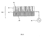
- a simplified scheme showing a method of obtaining a fingerprint is described.
- a strip of aluminium Tesa tape measuring 8 cm x 1.5 cm is anodized and subsequently electrodeposited with magnetic material according to the method described above:
- the processed strip is then mechanically sliced into 3 smaller and similarly sized strips and attached onto the top of an object 50 to be tagged.
- These strips now form 3 independent tags 500, 501 and 502.
- the tags 500, 501 and 502 are coated with a protective coating 55 and then magnetized (the magnetization process is symbolized by the arrow 52) by subjecting the tags to a uniform magnetic field 54 perpendicular to the plane of the tags.
- the magnetic field is provided for in the reader device in which a write head is installed. Then, the object is moved across beneath a read head 56. Alternatively, the read head is moved across the surface of the tags. The read head picks up magnetic field signals 57 corresponding to the characteristic of the magnetic field measured across the tags, and then stores the data representing these signals 57. The stored data forms the first identification information of the object.
- the tags are first magnetized and then read by the reader. Data obtained from the reading represents a second magnetic signal. This data is subsequently fed to a computer unit, which retrieves the data corresponding to the previously stored identification information. The computer compares both sets of data and computes the degree of fit between the them. If the match is above a tuneable tolerance level, the computer returns an authentication response indicating successful authentication.
- Example 2 Method of identifying: an object having identification information in which the identity tag is directly deposited onto the object
- the invention can also be implemented by preparing a porous tag in-situ on an object itself.
- the object on which a tag or a series of tags is created in-situ can be similar to the tagged object 50 in Fig. 5 .
- An electrically conductive adhesion layer such as titanium or chromium, is deposited first - this facilitates adhesion and electrodeposition of the magnetic material into the pores.
- Aluminium is deposited via physical vapour deposition (also known as sputtering) onto a small surface of the object to be tagged:
- the aluminium After the deposition of aluminium, the aluminium is subjected to an anodisation process in order to create the desired pores, thereby forming porous alumina.
- This porous alumina forms the host material of the tag.
- porous alumina is subjected to pulsed electrodeposition as mentioned above to deposit magnetic material, e.g. iron, into the pores.
- magnetic material e.g. iron
- the surface is polished by known methods, such as lapping or CMP.
- the surface is further coated with a protective layer of amorphous carbon and then, if necessary, a polyethylene layer, as described above to form a tag.
- a reader incorporating a read and write head is used to first magnetise the tag and then subsequently read the resulting magnetic signal from the tag, thereby obtaining the identification information of the object that is tagged.
- the tag is subject to an optional remagnetization step followed by reading in order to obtain a second specific magnetic signal from the tag.
- the data corresponding to the signal are fed to a computer, where they are compared with the stored identification information and authenticated accordingly.
- Example 3 A method of patterning a tag for storing recorded information and tagging information on a tag
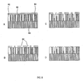
- Fig. 6A to Fig. 6D show embodiments of a tag 600 which is used to store recorded information and tagging information.
- the tag 600 that forms a magnetic strip 61 is comprised of porous host material in which the majority of pores are filled with magnetic material.
- Recorded information e.g. personal particulars, data related to the object that is tagged, or any dynamic data
- a strip of aluminium measuring 8 cm x 1.5 cm is anodised and has its pores electrodeposited with iron-nickel alloy according to Example 1.
- the processed strip 61 is then attached to a plastic card 60.
- Information that is to be written on the strip is translated by a suitable computer program into a corresponding digital signal 65.
- Magnetic material in the pores is magnetised into groups (domains) 63 and 64, wherein each group is orientated in a specific direction according to the digital signal 65.
- Neuron Electronics Inc.'s low-coercivity magnetic swipe card encoder/reader MCR230N is used.
- a 1cm x 0.5cm region 62 at one end of the strip is designated for producing/obtaining the unique tagging signal. Location marks described later may usefully be incorporated in this embodiment.
- a high resolution read head is used to read an analogue signal 66 of the linear magnetic field strength above the tag.
- recorded information is stored on the -strip 61 by patterning groups of pores in the host material with magnetic material according to a predetermined pattern.
- the medium storing the recorded and tagging information is comprised of a strip of porous host material in which intermittent groups of pores are filled with magnetic material. As shown in Fig. 6B , some groups of pores 67 are filled with magnetic material (shaded grey in the figure) while other groups of pores 68 are left empty (unshaded).
- the groups of filled pores are patterned to correspond to a desired digital signal 65 which is produced when reading the strip. This digital signal should in turn correspond to the static data or fixed label that is to be recorded onto the strip.
- a computer program can be used to assign each number and each letter of the alphabet to a specific digital signal pattern, thereby enabling the translation of human readable information to/from magnetic storage patterns.
- a lithographic process is used. First, the surface of the porous host material is capped with a masking layer prior to the deposition of magnetic material. This is achieved, for example, by evaporating an aluminium transfer layer onto the surface of the porous strip. A layer of positive resist (AR-U4040, All resist GmbH) is applied, by spin coating for example, onto the A1 transfer layer, and patterned accordingly by conventional photo-lithography.
- AR-U4040 All resist GmbH
- a wet chemical etch is subsequently performed using phosphoric acid and nitric acid and a small amount of wetting agent across the surface of the strip.
- the A1 transfer layer not covered by the resist can be completely removed after 30 min of etching. After etching, there remains on the strip an A1 transfer layer that is patterned with exposed regions. Finally, these exposed regions are then filled with magnetic material by electrodeposition.
- the MCR230N swipe reader from Neuron Electronics Inc. is used.
- the tagging signal a 1cm x 0.5cm region 62 at one end of the strip is designated and read by the above mentioned higher resolution read head to obtain the tagging signal.
- the tag does not reside on the same strip (which is made out of alumina as described in Example 1) containing the recorded information, but is located at another suitable position on the card.
- Fig. 6C shows a card having a tag region 691 located separately at the lower right hand corner of the card.
- This layout can be suitable for having the high resolution read head (for reading the tagging information) and magnetic swipe card read head (for reading the recorded information) mounted on a single actuator.
- the actuator When carrying out a reading of both the strip and tag, the actuator first positions the magnetic swipe card read head across the strip and then moves it across the strip. Subsequently, the actuator moves the analogue signal read head over the tag to obtain the tagging information. The reading is thus done consecutively.
- FIG. 6D shows a card having a tag region 692 located on the opposite side of the card.
- This layout can be suitable when it is desired to mount the two read heads on separate actuators.
- Each actuator can be located on opposite sides of the card and can move simultaneously and independently of each other, thus achieving a faster reading.
- the recorded information can also be read by a static magnetic swipe card read head and the action of an arm moving the card past the detector in the conventional manner.
- Example 4 A method of patterning a reference marking to guide a read head in locating a tag
- Figs. 7A to 7E show embodiments of different reference markings which can be separate from the tag or form part of the tag and be used for relocating the information on a tag. Reference markings are used if it is desired to increase the speed of locating the information on a tag on an object. As the size of tags can range from a few micrometers to several centimetres, a number of schemes can be used to direct the read heads towards the information on the tag.
- Figs. 7A to 7E can be detected for example by magnetic, optical or textural means. These shapes are designed to guide the read head to the information on the tag, shown as a square-shaped hatched region in each case.
- the reference markings are etched into a desired pattern using methods described previously, e.g. so that of magnetic material fills the pores in regions to form the desired pattern.
- This pattern forms the guide to the information on the tag 70 on a common substrate e.g. a plastic card.
- Fig. 7A shows a series of concentric rings 71 which target the information on the tag 70 at the centre. These rings may span much larger areas than the information on the tag.
- the spiral-shaped reference marking 72 guides a read head to move in an inward-spiral towards the information on the tag 70.
- fiducial marks 73 allow the position of the information on the tag 70 to be calculated through triangulation (dotted lines) of the cross-hair centres.
- a crosshair arrangement of fiducial marks 74 indicates the location of the information on the tag 70.
- the control system for moving the read head could be programmed to follow the specific location and movement rules appropriate for each marking system used.
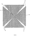
- Fig. 7E shows a further embodiment of a reference marking in which a V-shaped non-magnetic region 75 is patterned and used to direct the read head to the information on the tag 70.
- Fig. 7E The reference marking of Fig. 7E can be made and used in the invention as follows.
- a 1 cm x 1 cm square-shaped die is cut out of adhesive-backed copper tape is sputter coated with a one micrometer thick layer of aluminium.
- the wafer is then anodized to make the aluminium porous.
- Resist is spun coated onto the wafer and patterned using conventional photolithography leaving four V-shaped regions of photoresist 75 , each of which touches the four corners of the region designated to hold the information of the tag 70 at the centre.
- the entire cut wafer is then electrodeposited with magnetic material according to the procedures described in Example 1, the resist is removed, and then finally attached to an object to be tagged.
- a read head can be designed to move according to a set of rules as explained in the following.
- the read head is made to move along a path 77..Once it detects a non-magnetic region 75 , the read head switches to a programmed rule of detecting the boundary between the non-magnetic region 75 and the surrounding magnetic region 78 .
- the read head rebounds (deflects) at 90° (or any other suitable angle) away from its original line of motion.
- the distance travelled by the read head after each deflection becomes progressively shorter than the previous as the read head moves towards the tip of the V-shaped region. In this way, the read head is channelled towards the tag after several deflections.
- the read head is positioned at the desired starting position for reading the tag.
- Example 5 A method of varying the degree of pore filling in a tag
- Figs. 8A to 8D show a portion of a tag in which the process of varying the degree of pore filling in the tag is carried out.
- the following steps of varying the pore filling in the tag is based on photolithographic procedures.
- a 1.5 micrometer layer of aluminium is evaporated onto a 1 cm x 1 cm silicon wafer substrate 80 and processed into a tag comprising a host material 81 filled with a magnetic material 83 as explained in Example 1.
- nickel is used as the magnetic material.
- a layer of photoresist 82 is spincoated onto the surface of the tag.
- the photoresist is AR-U4040 from Allresist GmbH.
- Fig.8A shows the cross-section of a tag prepared in this manner.
- the photoresist is patterned according to a predetermined pattern using standard photolithography techniques available from the manufacturer or any text on silicon processing. After photolithographic pattern the photoresist mask contains a pattern of holes 84 (see Fig.8B ).
- the tag can be further subjected to hard baking to harden the remaining photoresist on the tag to protect the portions of the tag covered by the photoresist from the etching agent.
- an etching solution is used to remove nickel from pores that are not protected by the photoresist mask.
- the etching solution can be made by mixing the following chemicals: 5 parts HNO 3 , 5 parts CH 3 COOH, 2 parts H 2 SO 4 , 28 parts H 2 O.
- the tag is washed with distilled water.
- the tag now has the structure shown in Fig.8C .
- acetone is used to remove remaining photoresist (see Fig. 8D ).
- One method for achieving randomized openings is to bombard a polymer masking layer with high energy ions as described by Bernhardt et al., J. Vac. Sci. Technol. B, 18,1212-1215 (2000 ).
- the electrically conducting layer below the host material could be patterned into conducting and insulating regions prior to electrodeposition. This would cause some of the holes to remain unfilled or to be only partially filled with magnetic material.
- Fig.9 shows the cross section of a tag 900 in which an electrically conductive layer 91 below the filled pores is connected to a voltage source 94.
- the electrically conductive layer is in electrical contact with at least some of the material filling the pores.
- Such a tag is made and used to tag an object in the following manner.
- a strip of porous alumina host material 92 is prepared and then mounted on a substrate 90.
- the pores of the host material are electrodeposited with tin 93.
- the conductive layer 91 is electrically coupled to an AC voltage 94 to induce magnetic fields around the material within the pores.
- the induced magnetic fields could be measured using methods described above. These induced electromagnetic fields then become the unique tagging signal used to uniquely identify the tag.
- a uniform (static or pedistal) voltage, alternating voltage and a combination of the two can also be used to produce electric fields around the material within the pores.
- the electric fields could be measured by, for example, static capacitance measurements. These electric fields then become the characteristic used to uniquely identify the object on which the tag is attached.
- the material within the pores of the tags that are used in the above two methods need not necessarily be substantially Magnetic, as shown for the tag described in Example 1. It is sufficient that the material is electrically conductive in order for the tag to be used in the above method.
- the host material should, however, be substantially electrically insulating.
Landscapes
- Physics & Mathematics (AREA)
- General Physics & Mathematics (AREA)
- Engineering & Computer Science (AREA)
- Theoretical Computer Science (AREA)
- Credit Cards Or The Like (AREA)
- Magnetic Record Carriers (AREA)
- Manufacturing Of Magnetic Record Carriers (AREA)
Claims (32)
- Verfahren zum Identifizieren eines Gegenstands, der Identifikationsinformation besitzt, wobei die Identifikationsinformation verwendet wird, um die Identität des Gegenstands zu verifizieren, wobei das Verfahren umfasst:Bestimmen wenigstens einer Eigenschaft eines Magnetfeldes von zumindest einem Bereich eines Tags (100, 400, 500), wodurch ein erstes spezifisches magnetisches Signal erhalten wird, wobei das Tag ein Wirtsmaterial (11, 42, 81) mit einer ungeordneten Vielzahl von Poren (15, 20, 43) aufweist, wobei das Wirtsmaterial (11, 42, 81) im Wesentlichen nicht-magnetisch ist, wobei mindestens einige der ungeordneten Vielzahl von Poren mit einem magnetischen Material (10, 45, 83) gefüllt worden sind, undSpeichern von Signalinformation, die sich auf das erste spezifische magnetische Signal bezieht, wobei die gespeicherte Signalinformation die Identifikationsinformation des Gegenstands bildet.
- Verfahren nach Anspruch 1, wobei der Schritt, die mindestens eine Eigenschaft des Magnetfeldes des mindestens einen Bereichs des Tags (100, 400, 500) zu bestimmen, eine Messung der Eigenschaft des ortsspezifischen Magnetfeld über eine Oberfläche des Bereichs des Tags umfasst, wodurch ein magnetisches Fluktuationssignal zugeordnet wird.
- Verfahren nach Anspruch 1, wobei das Speichern der Signalinformation, die sich auf das erste spezifische magnetische Signal bezieht, umfasst, Daten zu speichern, die der mindestens einen Eigenschaft des Magnetfeldes über dem Bereich des Tags (100, 400, 500) entspricht.
- Verfahren nach Anspruch 1, ferner umfassend:Anschließend die mindestens eine Eigenschaft des Magnetfeldes des Bereich des Tags zu bestimmen, wodurch ein zweites spezifisches magnetisches Signal erhalten wird, undVergleichen des zweiten spezifischen magnetischen Signals mit der zuvor gespeicherten Identifikationsinformation.
- Verfahren nach Anspruch 4, ferner umfassend: Magnetisieren des Tags (100, 400, 500) vor jeder Bestimmung der mindestens einen Eigenschaft des Magnetfeldes des Bereichs des Tags (100, 400, 500).
- Verfahren nach Anspruch 1, ferner umfassend:Aufzeichnen von Information auf dem Tag (100, 400, 500) durch Magnetisieren des magnetischen Materials, das in Gruppen von Poren vorhanden ist, in gepolten Domänen oderStrukturieren von Poren des Tags (100, 400, 500) mit magnetischem Material.
- Verfahren nach Anspruch 1, wobei das Tag (100, 400, 500) an den zu identifizierenden Gegenstand angebracht wird, nachdem das erste spezifischen magnetische Signal erhalten worden ist.
- Verfahren nach Anspruch 1, wobei das Tag (100, 400, 500) an den zu identifizierenden Gegenstand angebracht wird, bevor das erste spezifischen magnetische Signal erhalten worden ist.
- Verfahren nach Anspruch 1, wobei das Tag ein Substrat (80) umfasst, auf dem das Wirtsmaterials angebracht ist.
- Verfahren nach Anspruch 9, wobei das Substrat ein Material umfasst, das aus der Gruppe ausgewählt wird, die aus Metall Silizium, Siliziumdioxid, Glas, Kunststoff, Keramik und Kombinationen davon besteht.
- Verfahren nach Anspruch 1, wobei das Wirtsmaterial ausgewählt wird aus der Gruppe, die aus Aluminiumoxid, Zeolithen, Gruppe III-V-Materialien, Polymeren, Siliziumoxid, Zinkoxid und Zinnoxid besteht.
- Verfahren nach Anspruch 1, wobei das Wirtsmaterial Nanoröhren umfasst.
- Das Verfahren gemäß Anspruch 12, wobei die Nanoröhren innerhalb eines zweiten Wirtsmaterials gegossen sind.
- Verfahren nach Anspruch 1, wobei das magnetische Material aus der Gruppe bestehend aus Fe, Ni, Co, deren Legierungen, Oxiden, Mischungen und Kombinationen davon.
- Verfahren nach Anspruch 1, wobei die Poren des Wirtsmaterials einen Durchmesser zwischen 10nm und 500nm aufweisen.
- Verfahren nach Anspruch 1, wobei das Tag (100, 400, 500) ferner zumindest eine Überzugsschicht (82) besitzt.
- Verfahren nach Anspruch 1, wobei die mindestens eine Eigenschaft des Magnetfeldes des Bereichs des Tags stark abhängig von der Unordnung des Tags ist.
- Das Verfahren gemäß Anspruch 17, worin die Unordnung auf ein Merkmals zurückzuführen ist, das aus der Gruppe ausgewählt wird, die aus Porengröße, Form und Orientierung der Poren, Prozentsatz der Porenfüllung, Kristallorientierung des magnetischen Material in dem Tag und Kombinationen davon besteht.
- Verfahren zum Identifizieren eines Gegenstands, der Identifikationsinformation besitzt, wobei die Identifikationsinformation verwendet wird, um die Identität des Gegenstands zu verifizieren, wobei das Verfahren umfasst:Bestimmen wenigstens einer Eigenschaft eines elektrischen oder elektromagnetischen Felds von zumindest einem Bereich eines Tags (900), wodurch ein erstes spezifisches elektrisches oder elektromagnetisches Signal erhalten wird, wobei das Tag ein Wirtsmaterial (92) mit einer ungeordneten Vielzahl von Poren (15, 20, 43) aufweist, wobei das Wirtsmaterial (92) im Wesentlichen elektrisch isolierend ist, wobei mindestens einige der ungeordneten Vielzahl von Poren mit einem im Wesentlichen elektrisch leitenden Material (93) gefüllt worden sind, und wobei wenigstens einiges des im Wesentlichen elektrisch leitenden Material (93) mit einer Spannungsquelle (94) verbunden ist,Speichern von Signalinformation, die sich auf das erste spezifische elektrische oder elektromagnetische Signal bezieht, wobei die gespeicherte Signalinformation die Identifikationsinformation des Gegenstands bildet.
- Verfahren nach Anspruch 19, wobei der Schritt, die mindestens eine Eigenschaft des elektrischen oder elektromagnetischen Felds des mindestens einen Bereichs des Tags (900) zu bestimmen, eine Messung der Eigenschaft des ortsspezifischen elektrischen oder elektromagnetischen Felds über eine Oberfläche des Bereichs des Tags (900) umfasst, wodurch ein elektrisches Fluktuationssignal zugeordnet wird.
- Verfahren nach Anspruch 19, wobei das Speichern der Signalinformation, die sich auf das erste spezifische elektrische oder elektromagnetische Signal bezieht, umfasst, Daten zu speichern, die der mindestens einen Eigenschaft des elektrischen oder elektromagnetischen Felds über dem Bereich des Tags (900) entspricht.
- Verfahren nach Anspruch 19, ferner umfassend:anschließend die mindestens eine Eigenschaft des elektrischen oder elektromagnetischen Felds des Bereich des Tags (900) zu bestimmen, wodurch ein zweites spezifisches elektrisches oder elektromagnetisches Signal erhalten wird, undVergleichen des zweiten spezifischen des elektrischen oder elektromagnetischen Felds Signals mit der zuvor gespeicherten Identifikationsinformation.
- Verfahren zur Herstellung eines Systems zur Gegenstandsidentifikation, wobei das System ein Tag (100, 400, 500), das Identifikationsinformation trägt, sowie ein Datenspeichermedium zum Speichern von Daten, die einem magnetischen Signal entsprechen, das von mindestens einem Bereich des Tags (100, 400, 500) erhalten worden ist, wobei das Verfahren umfasst:Bestimmen wenigstens einer Eigenschaft eines Magnetfeldes von zumindest einem Bereich eines Tags (100, 400, 500), wodurch ein erstes spezifisches magnetisches Signal erhalten wird, wobei das Tag ein Wirtsmaterial (11, 42, 81) mit einer ungeordneten Vielzahl von Poren (15, 20, 43) aufweist, wobei das Wirtsmaterial (11, 42, 81) im Wesentlichen nicht-magnetisch ist, wobei mindestens einige der ungeordneten Vielzahl von Poren mit einem magnetischen Material (10, 45, 83) gefüllt worden sind, undSpeichern von Signalinformation, die sich auf das erste spezifische magnetische Signal bezieht, wobei die gespeicherte Signalinformation die Identifikationsinformation eines zu identifizierenden Gegenstands bildet.
- Verfahren zur Herstellung eines Systems zur Gegenstandsidentifikation, wobei das System ein Tag (900), das Identifikationsinformation trägt, sowie ein Datenspeichermedium zum Speichern von Daten, die einem elektrischen oder elektromagnetischen Signal entsprechen, das von mindestens einem Bereich des Tags (900) erhalten worden ist, wobei das Verfahren umfasst:Bestimmen wenigstens einer Eigenschaft eines elektrischen oder elektromagnetischen Felds von zumindest einem Bereich eines Tags (900), wodurch ein erstes spezifisches elektrisches oder elektromagnetisches Signal erhalten wird, wobei das Tag ein Wirtsmaterial (92) mit einer ungeordneten Vielzahl von Poren (15, 20, 43) aufweist, wobei das Wirtsmaterial (92) im Wesentlichen elektrisch isolierend ist, wobei mindestens einige der ungeordneten Vielzahl von Poren mit einem im Wesentlichen elektrisch leitenden Material (93) gefüllt worden sind, und wobei wenigstens einiges des im Wesentlichen elektrisch leitenden Material (93) mit einer Spannungsquelle (94) verbunden ist,Speichern von Signalinformation, die sich auf das erste spezifische elektrische oder elektromagnetische Signal bezieht, wobei die gespeicherte Signalinformation die Identifikationsinformation eines zu identifizierenden Gegenstands bildet.
- Ein Tag (100, 400, 500), das Identifikationsinformation trägt, wobei das Tag (100 400, 500) umfasst:ein Wirtsmaterial (11, 42, 81), das im Wesentlichen nicht-magnetisch ist, und eine Überzugsschicht (82), die zumindest teilweise eine Oberfläche des Wirtsmaterials (11, 42, 81) bedeckt, dadurch gekennzeichnet, dassdas Wirtsmaterial (11, 42, 81) eine ungeordnete Vielzahl von Poren (15, 20, 43) besitzt und mindestens einige der ungeordneten Vielzahl von Poren des Wirtsmaterials mit einem magnetischen Material (10, 45, 83) gefüllt worden sind, um die Identifikationsinformation zu bilden.
- Tag nach Anspruch 25, wobei die Überzugsschicht ein Material umfasst, das eine Bulk-Streckgrenze von mehr als 50 mN/m2 hat.
- Ein Tag (900), das Identifikationsinformation trägt, wobei das Tag (900) umfasst:ein Wirtsmaterial, das im Wesentlichen elektrisch isolierend ist, und eine Überzugsschicht (82), die zumindest teilweise eine Oberfläche des Wirtsmaterials (92) bedeckt, dadurch gekennzeichnet, dass das Wirtsmaterial (92) eine ungeordnete Vielzahl von Poren besitzt und mindestens einige der ungeordneten Vielzahl von Poren des Wirtsmaterials mit einem elektrisch leitenden Material (93) gefüllt worden sind, um die Identifikationsinformation zu bilden.
- Tag nach Anspruch 27, wobei die Überzugsschicht ein Material umfasst, das eine Bulk-Streckgrenze von mehr als 50 mN/m2 hat.
- Gegenstand mit einem Tag (100, 400, 500) gemäß Anspruch 25.
- Gegenstand mit einem Tag (900) gemäß Anspruch 27.
- System zu Gegenstandsidentifizierung, wobei das System umfasst:ein Tag (100, 400, 500), das Identifikationsinformation trägt, wobei das Tag ein Wirtsmaterial (11, 42, 81) mit einer ungeordneten Vielzahl von Poren (15, 20, 43) aufweist,wobei das Wirtsmaterial (11, 42, 81) im Wesentlichen nicht-magnetisch ist, wobei mindestens einige der ungeordneten Vielzahl von Poren mit einem magnetischen Material (10, 45, 83) gefüllt worden sind, um die Identifikationsinformation zu bilden undein Datenspeichermedium zum Speichern von Daten, die einem magnetischen Signal entsprechen, das von mindestens einem Bereich des Tags erhalten worden ist.
- ystem zu Gegenstandsidentifizierung, wobei das System umfasst:ein Tag (900), das Identifikationsinformation trägt, wobei das Tag ein Wirtsmaterial (92) mit einer ungeordneten Vielzahl von Poren aufweist, wobei das Wirtsmaterial (92) im Wesentlichen elektrisch isolierend ist,wobei mindestens einige der ungeordneten Vielzahl von Poren mit einem in Wesentlichen elektrisch leitenden Material (93) gefüllt worden sind, um die Identifikationsinformation zu bilden, wobei wenigstens einiges des im Wesentlichen elektrisch leitenden Material (93) mit einer Spannungsquelle (94) verbunden ist, undein Datenspeichermedium zum Speichern von Daten, die einem elektrischen oder elektromagnetischen Signal entsprechen, das von mindestens einem Bereich des Tags erhalten worden ist.
Applications Claiming Priority (2)
| Application Number | Priority Date | Filing Date | Title |
|---|---|---|---|
| US10/625,235 US7865722B2 (en) | 2003-07-22 | 2003-07-22 | Method of identifying an object and a tag carrying identification information |
| PCT/SG2004/000216 WO2005008294A1 (en) | 2003-07-22 | 2004-07-16 | A method of identifying an object and a tag carrying identification information |
Publications (3)
| Publication Number | Publication Date |
|---|---|
| EP1646891A1 EP1646891A1 (de) | 2006-04-19 |
| EP1646891A4 EP1646891A4 (de) | 2009-01-28 |
| EP1646891B1 true EP1646891B1 (de) | 2012-11-07 |
Family
ID=34080161
Family Applications (1)
| Application Number | Title | Priority Date | Filing Date |
|---|---|---|---|
| EP04749238A Not-in-force EP1646891B1 (de) | 2003-07-22 | 2004-07-16 | Verfahren zum identifizieren eines objekts und eines etiketts, das identifikationsinformationen trägt |
Country Status (5)
| Country | Link |
|---|---|
| US (1) | US7865722B2 (de) |
| EP (1) | EP1646891B1 (de) |
| JP (1) | JP4917430B2 (de) |
| CN (1) | CN100399057C (de) |
| WO (1) | WO2005008294A1 (de) |
Families Citing this family (43)
| Publication number | Priority date | Publication date | Assignee | Title |
|---|---|---|---|---|
| PL1908044T3 (pl) * | 2005-06-29 | 2011-09-30 | Eidgenoessische Technische Hochschule Zuerich | Unikalne etykiety dla systemu identyfikacji lub ochrony |
| US20070105229A1 (en) * | 2005-08-19 | 2007-05-10 | Burns Carolyn A | Authentication of packaged articles |
| GB0523631D0 (en) * | 2005-11-21 | 2005-12-28 | Univ Cambridge Tech | Magnetic tagging techniques |
| WO2007133164A1 (en) * | 2006-05-11 | 2007-11-22 | Singular Id Pte Ltd | Identification tags, objects adapted to be identified, and related methods, devices and systems |
| EP2016539A4 (de) * | 2006-05-11 | 2010-06-09 | Singular Id Pte Ltd | Verfahren zum identifizieren eines objekts, identifikationsetikett, für identifikation ausgelegtes objekt und diesbezügliche einrichtung und system |
| DE102006030365B3 (de) * | 2006-06-27 | 2007-12-06 | Siemens Ag | Verfahren zum Herstellen eines Gussteiles |
| US7950587B2 (en) * | 2006-09-22 | 2011-05-31 | The Board of Regents of the Nevada System of Higher Education on behalf of the University of Reno, Nevada | Devices and methods for storing data |
| EP2637145B1 (de) | 2007-04-24 | 2022-01-12 | Sicpa Holding Sa | Verfahren zur Markierung und zur Idenfizieurung eines Dokument oder Artikels mit kreisförmigen polarisierenden Teilchen |
| CN101715589B (zh) | 2007-04-24 | 2014-01-22 | 锡克拜控股有限公司 | 标记物品的方法;用于标识所标记的物品的方法和设备;圆偏振粒子的使用 |
| US7874496B2 (en) * | 2008-01-04 | 2011-01-25 | Microsoft Corporation | Optically readable tag |
| DE102009020208A1 (de) * | 2009-05-07 | 2010-11-11 | Merck Patent Gmbh | Verfahren zum Codieren von Produkten |
| JP2011170905A (ja) * | 2010-02-16 | 2011-09-01 | Fuji Electric Device Technology Co Ltd | ディスクリートトラック構造を有する磁気記録媒体の製造方法 |
| SG186283A1 (en) | 2010-06-14 | 2013-01-30 | Trutag Technologies Inc | System for producing a packaged item with an identifier |
| CA2810798A1 (en) * | 2010-09-08 | 2012-03-15 | Bilcare Technologies Singapore Pte. Ltd. | An integrated unit for reading identification information based on inherent disorder |
| WO2012082076A1 (en) * | 2010-12-16 | 2012-06-21 | Bilcare Technologies Singapore Pte. Ltd. | Mass production of tags based on inherent disorder and readers for such tags |
| US9247041B2 (en) | 2011-03-24 | 2016-01-26 | Bilcare Technologies Singapore Pte. Ltd. | Inherent disorder reader adapted to be connected to a mobile device |
| US8931696B2 (en) | 2011-08-17 | 2015-01-13 | Darden Gwaltney Hood | Counterfeit detection system and method |
| US8439258B1 (en) * | 2011-08-17 | 2013-05-14 | Darden Gwaltney Hood | Counterfeit detection system and method |
| US8851384B2 (en) * | 2011-12-13 | 2014-10-07 | Empire Technology Development Llc | Coded fibers |
| WO2013095172A1 (ru) * | 2011-12-19 | 2013-06-27 | Pleten Oleg Ivanovich | Определение давности события создания объекта, содержащего целлюлозу, для защиты изделия от фальсификации |
| CN103473589B (zh) * | 2013-09-10 | 2016-09-14 | 江苏多维科技有限公司 | 一种磁条形码芯片及其读取方法 |
| CN103593905B (zh) * | 2013-10-28 | 2016-05-04 | 深圳力合防伪技术有限公司 | 反铁磁共振射频识别票证管理系统和方法 |
| CN106462781B (zh) * | 2014-04-22 | 2019-08-30 | 先进工程解决方案有限责任公司 | 用于工业过程中类皮革和皮革材料的可追踪性的方法 |
| EP3207391B1 (de) * | 2014-10-16 | 2022-03-02 | Sikorsky Aircraft Corporation | Magnetische identifizierungsanordnung und verfahren zur identifizierung einer komponente |
| KR101713033B1 (ko) * | 2015-06-09 | 2017-04-04 | 주식회사 씨에프에이 | 위변조방지 태그 제작용 복합함량 동철합금 성형재 |
| US10410779B2 (en) | 2015-10-09 | 2019-09-10 | Lexmark International, Inc. | Methods of making physical unclonable functions having magnetic and non-magnetic particles |
| US9553582B1 (en) | 2015-10-09 | 2017-01-24 | Lexmark International, Inc. | Physical unclonable functions having magnetic and non-magnetic particles |
| US20170102668A1 (en) * | 2015-10-09 | 2017-04-13 | Lexmark International, Inc. | Physical Unclonable Function of a Supply Item |
| US9608634B1 (en) * | 2015-10-09 | 2017-03-28 | Lexmark International, Inc. | Toothed-rack physical unclonable function |
| US9608828B1 (en) * | 2015-10-09 | 2017-03-28 | Lexmark International, Inc. | Elongated physical unclonable function |
| US20170100862A1 (en) | 2015-10-09 | 2017-04-13 | Lexmark International, Inc. | Injection-Molded Physical Unclonable Function |
| US9929864B2 (en) | 2015-10-09 | 2018-03-27 | Lexmark International, Inc. | Rotating magnetic measurements of physical unclonable functions |
| US9917699B2 (en) * | 2015-10-09 | 2018-03-13 | Lexmark International, Inc. | Physical unclonable function imaged through two faces |
| US10360491B2 (en) * | 2016-02-05 | 2019-07-23 | Feng Jiang | Method for providing random combination status code for commodity |
| US9665748B1 (en) | 2016-08-03 | 2017-05-30 | Lexmark International, Inc. | Magnetic helical physical unclonable function measured adjacent to flight |
| US9524456B1 (en) | 2016-08-03 | 2016-12-20 | Lexmark International, Inc. | Manufacturing a helical physical unclonable function |
| US9542576B1 (en) | 2016-08-03 | 2017-01-10 | Lexmark International, Inc. | Magnetic helical physical unclonable function measured above flight |
| JP7048064B2 (ja) * | 2016-09-30 | 2022-04-05 | 株式会社環境レジリエンス | 個別認証媒体を用いた個別認証システム |
| US10212300B2 (en) | 2016-12-09 | 2019-02-19 | Lexmark International, Inc. | Magnetic keys having a plurality of magnetic plates |
| US10102466B2 (en) | 2016-12-09 | 2018-10-16 | Lexmark International, Inc. | Magnetic keys having a plurality of magnet layers with holes |
| CN106652768B (zh) * | 2017-01-24 | 2023-01-03 | 中信戴卡股份有限公司 | 一种用于铝合金产品的标记部件 |
| US20190139909A1 (en) | 2017-11-09 | 2019-05-09 | Lexmark International, Inc. | Physical Unclonable Functions in Integrated Circuit Chip Packaging for Security |
| US10929735B1 (en) | 2020-02-03 | 2021-02-23 | Capital One Services, Llc | Smart card with sensors for detecting environmental conditions |
Family Cites Families (29)
| Publication number | Priority date | Publication date | Assignee | Title |
|---|---|---|---|---|
| GB1216403A (en) | 1967-04-10 | 1970-12-23 | Gen Electric | Transit ticket having an information encodable matrix for automatic fare collection systems |
| US3651312A (en) | 1967-06-30 | 1972-03-21 | Walter W Barney | Magnetically coded card structure |
| US3601913A (en) * | 1968-07-22 | 1971-08-31 | Fmc Corp | Magnetic transaction card and method in forming the same |
| US3940795A (en) * | 1970-04-21 | 1976-02-24 | Lemelson Jerome H | Verification apparatus using a card scanning means |
| US4264648A (en) * | 1976-09-10 | 1981-04-28 | Xerox Corporation | Low specific gravity magnetic carrier materials |
| NL8502567A (nl) * | 1985-09-19 | 1987-04-16 | Bekaert Sa Nv | Werkwijze en inrichting voor het op echtheid controleren van voorwerpen en voorwerp geschikt voor het toepassen van deze werkwijze. |
| US4985614A (en) | 1987-01-16 | 1991-01-15 | Rand Mcnally & Company | Object verification apparatus and method |
| JPS6429710A (en) | 1987-07-24 | 1989-01-31 | Alps Electric Co Ltd | Magnetic recording medium for magnetic type encoder |
| DE68919753T2 (de) | 1988-06-03 | 1995-04-27 | Hitachi Maxell | Magnetischer Aufzeichnungsträger und Verfahren zu seiner Herstellung. |
| US5204663A (en) * | 1990-05-21 | 1993-04-20 | Applied Systems Institute, Inc. | Smart card access control system |
| US5235166A (en) | 1991-02-14 | 1993-08-10 | Xtec Incorporated | Data verification method and magnetic media therefor |
| US5734020A (en) * | 1991-11-20 | 1998-03-31 | Cpg, Inc. | Production and use of magnetic porous inorganic materials |
| JPH06138823A (ja) * | 1992-10-23 | 1994-05-20 | Murata Mfg Co Ltd | タ グ |
| JPH0823880B2 (ja) * | 1993-01-08 | 1996-03-06 | 有限会社原田製作所 | 物品等の管理用板 |
| US5546462A (en) | 1993-04-09 | 1996-08-13 | Washington University | Method and apparatus for fingerprinting and authenticating various magnetic media |
| US5451759A (en) * | 1993-06-24 | 1995-09-19 | Nhk Spring Co., Ltd. | Using high-permeability magnetic elements randomly scattered in the objects |
| US5480685A (en) * | 1993-10-22 | 1996-01-02 | Tomoegawa Paper Co., Ltd. | Method of making a magnetic recording medium comprising two magnetic layers |
| US5601931A (en) * | 1993-12-02 | 1997-02-11 | Nhk Spring Company, Ltd. | Object to be checked for authenticity and a method for manufacturing the same |
| US5920628A (en) | 1997-01-09 | 1999-07-06 | Washington University | Method and apparatus for fingerprinting and authenticating various magnetic media |
| US7778418B1 (en) * | 1998-01-08 | 2010-08-17 | Samsung Electronics Co., Ltd. | System and method for copy protection for digital signals |
| JP2000182006A (ja) * | 1998-12-15 | 2000-06-30 | Shinozaki Seisakusho:Kk | 情報カ―ドの正当性判定システム、情報カ―ド、及び情報カ―ドの製造方法 |
| US6602620B1 (en) * | 1998-12-28 | 2003-08-05 | Kabushiki Kaisha Toshiba | Magnetic recording apparatus, magnetic recording medium and manufacturing method thereof |
| US6328209B1 (en) | 1999-02-03 | 2001-12-11 | American Bank Note Holographics, Inc. | Card security system |
| US6959384B1 (en) * | 1999-12-14 | 2005-10-25 | Intertrust Technologies Corporation | Systems and methods for authenticating and protecting the integrity of data streams and other data |
| US7225082B1 (en) | 1999-10-01 | 2007-05-29 | Oxonica, Inc. | Colloidal rod particles as nanobar codes |
| JP2002074936A (ja) * | 2000-08-31 | 2002-03-15 | Canon Inc | 磁気デバイス |
| US6976167B2 (en) * | 2001-06-26 | 2005-12-13 | Intel Corporation | Cryptography-based tamper-resistant software design mechanism |
| US7018838B2 (en) * | 2002-05-22 | 2006-03-28 | Platypus Technologies, Llc | Substrates, devices, and methods for cellular assays |
| EP1494460A1 (de) * | 2003-07-02 | 2005-01-05 | THOMSON Licensing S.A. | Verfahren oder Vorrichtung zur Authentifizierung digitaler Daten mittels eines Authentifizierungs-Plugins |
-
2003
- 2003-07-22 US US10/625,235 patent/US7865722B2/en not_active Expired - Fee Related
-
2004
- 2004-07-16 JP JP2006521042A patent/JP4917430B2/ja not_active Expired - Fee Related
- 2004-07-16 WO PCT/SG2004/000216 patent/WO2005008294A1/en active Application Filing
- 2004-07-16 CN CNB2004800209384A patent/CN100399057C/zh not_active Expired - Fee Related
- 2004-07-16 EP EP04749238A patent/EP1646891B1/de not_active Not-in-force
Also Published As
| Publication number | Publication date |
|---|---|
| JP2007504520A (ja) | 2007-03-01 |
| EP1646891A4 (de) | 2009-01-28 |
| WO2005008294A1 (en) | 2005-01-27 |
| CN100399057C (zh) | 2008-07-02 |
| EP1646891A1 (de) | 2006-04-19 |
| US20050017082A1 (en) | 2005-01-27 |
| JP4917430B2 (ja) | 2012-04-18 |
| US7865722B2 (en) | 2011-01-04 |
| CN1826539A (zh) | 2006-08-30 |
Similar Documents
| Publication | Publication Date | Title |
|---|---|---|
| EP1646891B1 (de) | Verfahren zum identifizieren eines objekts und eines etiketts, das identifikationsinformationen trägt | |
| US7891567B2 (en) | Identification tag, object adapted to be identified, and related methods, devices, and systems | |
| JP5235868B2 (ja) | オブジェクト識別方法並びに読み取りデバイス | |
| US8763903B2 (en) | Reading device for identifying a tag or an object adapted to be identified, related methods and systems | |
| DE60318592T2 (de) | Sicherheitseinrichtung und system | |
| USRE39490E1 (en) | Security device having multiple security features and method of making same | |
| US20090309733A1 (en) | Identification tags, objects adapted to be identified, and related methods, devices and systems | |
| RU2638848C1 (ru) | Ценный документ, защищённый от подделки, и способ определения его подлинности | |
| EP1662486A1 (de) | Prozess zur Speicherung van Information in einer magnetischen Multischichtanordnung | |
| JP2888501B2 (ja) | 磁性変態金属でなる物品 | |
| US20170061724A1 (en) | Article identification reader, marker element for article identification and method of article identification | |
| JPH1069603A (ja) | 磁気カード及び磁気カード不正防止方法 | |
| US20080084634A1 (en) | Devices and methods for storing data | |
| JP2000082208A (ja) | 磁気バーコード及びその記録方法 |
Legal Events
| Date | Code | Title | Description |
|---|---|---|---|
| PUAI | Public reference made under article 153(3) epc to a published international application that has entered the european phase |
Free format text: ORIGINAL CODE: 0009012 |
|
| 17P | Request for examination filed |
Effective date: 20060111 |
|
| AK | Designated contracting states |
Kind code of ref document: A1 Designated state(s): AT BE BG CH CY CZ DE DK EE ES FI FR GB GR HU IE IT LI LU MC NL PL PT RO SE SI SK TR |
|
| DAX | Request for extension of the european patent (deleted) | ||
| RIN1 | Information on inventor provided before grant (corrected) |
Inventor name: MORAN, P. M. Inventor name: BURDEN, A.P. |
|
| A4 | Supplementary search report drawn up and despatched |
Effective date: 20090105 |
|
| 17Q | First examination report despatched |
Effective date: 20091210 |
|
| GRAP | Despatch of communication of intention to grant a patent |
Free format text: ORIGINAL CODE: EPIDOSNIGR1 |
|
| GRAS | Grant fee paid |
Free format text: ORIGINAL CODE: EPIDOSNIGR3 |
|
| GRAA | (expected) grant |
Free format text: ORIGINAL CODE: 0009210 |
|
| AK | Designated contracting states |
Kind code of ref document: B1 Designated state(s): AT BE BG CH CY CZ DE DK EE ES FI FR GB GR HU IE IT LI LU MC NL PL PT RO SE SI SK TR |
|
| REG | Reference to a national code |
Ref country code: GB Ref legal event code: FG4D |
|
| REG | Reference to a national code |
Ref country code: CH Ref legal event code: EP Ref country code: AT Ref legal event code: REF Ref document number: 583225 Country of ref document: AT Kind code of ref document: T Effective date: 20121115 |
|
| REG | Reference to a national code |
Ref country code: CH Ref legal event code: NV Representative=s name: ALDO ROEMPLER PATENTANWALT, CH |
|
| REG | Reference to a national code |
Ref country code: IE Ref legal event code: FG4D |
|
| REG | Reference to a national code |
Ref country code: DE Ref legal event code: R096 Ref document number: 602004039953 Country of ref document: DE Effective date: 20130103 |
|
| REG | Reference to a national code |
Ref country code: AT Ref legal event code: MK05 Ref document number: 583225 Country of ref document: AT Kind code of ref document: T Effective date: 20121107 |
|
| REG | Reference to a national code |
Ref country code: NL Ref legal event code: VDEP Effective date: 20121107 |
|
| PG25 | Lapsed in a contracting state [announced via postgrant information from national office to epo] |
Ref country code: FI Free format text: LAPSE BECAUSE OF FAILURE TO SUBMIT A TRANSLATION OF THE DESCRIPTION OR TO PAY THE FEE WITHIN THE PRESCRIBED TIME-LIMIT Effective date: 20121107 Ref country code: SE Free format text: LAPSE BECAUSE OF FAILURE TO SUBMIT A TRANSLATION OF THE DESCRIPTION OR TO PAY THE FEE WITHIN THE PRESCRIBED TIME-LIMIT Effective date: 20121107 Ref country code: NL Free format text: LAPSE BECAUSE OF FAILURE TO SUBMIT A TRANSLATION OF THE DESCRIPTION OR TO PAY THE FEE WITHIN THE PRESCRIBED TIME-LIMIT Effective date: 20121107 |
|
| PG25 | Lapsed in a contracting state [announced via postgrant information from national office to epo] |
Ref country code: PT Free format text: LAPSE BECAUSE OF FAILURE TO SUBMIT A TRANSLATION OF THE DESCRIPTION OR TO PAY THE FEE WITHIN THE PRESCRIBED TIME-LIMIT Effective date: 20130307 Ref country code: GR Free format text: LAPSE BECAUSE OF FAILURE TO SUBMIT A TRANSLATION OF THE DESCRIPTION OR TO PAY THE FEE WITHIN THE PRESCRIBED TIME-LIMIT Effective date: 20130208 Ref country code: PL Free format text: LAPSE BECAUSE OF FAILURE TO SUBMIT A TRANSLATION OF THE DESCRIPTION OR TO PAY THE FEE WITHIN THE PRESCRIBED TIME-LIMIT Effective date: 20121107 Ref country code: CY Free format text: LAPSE BECAUSE OF FAILURE TO SUBMIT A TRANSLATION OF THE DESCRIPTION OR TO PAY THE FEE WITHIN THE PRESCRIBED TIME-LIMIT Effective date: 20121107 Ref country code: BE Free format text: LAPSE BECAUSE OF FAILURE TO SUBMIT A TRANSLATION OF THE DESCRIPTION OR TO PAY THE FEE WITHIN THE PRESCRIBED TIME-LIMIT Effective date: 20121107 Ref country code: SI Free format text: LAPSE BECAUSE OF FAILURE TO SUBMIT A TRANSLATION OF THE DESCRIPTION OR TO PAY THE FEE WITHIN THE PRESCRIBED TIME-LIMIT Effective date: 20121107 |
|
| PG25 | Lapsed in a contracting state [announced via postgrant information from national office to epo] |
Ref country code: AT Free format text: LAPSE BECAUSE OF FAILURE TO SUBMIT A TRANSLATION OF THE DESCRIPTION OR TO PAY THE FEE WITHIN THE PRESCRIBED TIME-LIMIT Effective date: 20121107 |
|
| PG25 | Lapsed in a contracting state [announced via postgrant information from national office to epo] |
Ref country code: DK Free format text: LAPSE BECAUSE OF FAILURE TO SUBMIT A TRANSLATION OF THE DESCRIPTION OR TO PAY THE FEE WITHIN THE PRESCRIBED TIME-LIMIT Effective date: 20121107 Ref country code: EE Free format text: LAPSE BECAUSE OF FAILURE TO SUBMIT A TRANSLATION OF THE DESCRIPTION OR TO PAY THE FEE WITHIN THE PRESCRIBED TIME-LIMIT Effective date: 20121107 Ref country code: BG Free format text: LAPSE BECAUSE OF FAILURE TO SUBMIT A TRANSLATION OF THE DESCRIPTION OR TO PAY THE FEE WITHIN THE PRESCRIBED TIME-LIMIT Effective date: 20130207 Ref country code: SK Free format text: LAPSE BECAUSE OF FAILURE TO SUBMIT A TRANSLATION OF THE DESCRIPTION OR TO PAY THE FEE WITHIN THE PRESCRIBED TIME-LIMIT Effective date: 20121107 Ref country code: CZ Free format text: LAPSE BECAUSE OF FAILURE TO SUBMIT A TRANSLATION OF THE DESCRIPTION OR TO PAY THE FEE WITHIN THE PRESCRIBED TIME-LIMIT Effective date: 20121107 |
|
| PG25 | Lapsed in a contracting state [announced via postgrant information from national office to epo] |
Ref country code: RO Free format text: LAPSE BECAUSE OF FAILURE TO SUBMIT A TRANSLATION OF THE DESCRIPTION OR TO PAY THE FEE WITHIN THE PRESCRIBED TIME-LIMIT Effective date: 20121107 |
|
| PLBE | No opposition filed within time limit |
Free format text: ORIGINAL CODE: 0009261 |
|
| STAA | Information on the status of an ep patent application or granted ep patent |
Free format text: STATUS: NO OPPOSITION FILED WITHIN TIME LIMIT |
|
| 26N | No opposition filed |
Effective date: 20130808 |
|
| PG25 | Lapsed in a contracting state [announced via postgrant information from national office to epo] |
Ref country code: ES Free format text: LAPSE BECAUSE OF FAILURE TO SUBMIT A TRANSLATION OF THE DESCRIPTION OR TO PAY THE FEE WITHIN THE PRESCRIBED TIME-LIMIT Effective date: 20130218 |
|
| PGFP | Annual fee paid to national office [announced via postgrant information from national office to epo] |
Ref country code: CH Payment date: 20130719 Year of fee payment: 10 Ref country code: DE Payment date: 20130722 Year of fee payment: 10 Ref country code: IE Payment date: 20130726 Year of fee payment: 10 |
|
| PGFP | Annual fee paid to national office [announced via postgrant information from national office to epo] |
Ref country code: GB Payment date: 20130719 Year of fee payment: 10 Ref country code: FR Payment date: 20130722 Year of fee payment: 10 |
|
| REG | Reference to a national code |
Ref country code: DE Ref legal event code: R097 Ref document number: 602004039953 Country of ref document: DE Effective date: 20130808 |
|
| PGFP | Annual fee paid to national office [announced via postgrant information from national office to epo] |
Ref country code: IT Payment date: 20130730 Year of fee payment: 10 |
|
| PG25 | Lapsed in a contracting state [announced via postgrant information from national office to epo] |
Ref country code: MC Free format text: LAPSE BECAUSE OF FAILURE TO SUBMIT A TRANSLATION OF THE DESCRIPTION OR TO PAY THE FEE WITHIN THE PRESCRIBED TIME-LIMIT Effective date: 20121107 |
|
| REG | Reference to a national code |
Ref country code: DE Ref legal event code: R119 Ref document number: 602004039953 Country of ref document: DE |
|
| REG | Reference to a national code |
Ref country code: CH Ref legal event code: PL |
|
| GBPC | Gb: european patent ceased through non-payment of renewal fee |
Effective date: 20140716 |
|
| REG | Reference to a national code |
Ref country code: IE Ref legal event code: MM4A |
|
| REG | Reference to a national code |
Ref country code: FR Ref legal event code: ST Effective date: 20150331 |
|
| PG25 | Lapsed in a contracting state [announced via postgrant information from national office to epo] |
Ref country code: IT Free format text: LAPSE BECAUSE OF NON-PAYMENT OF DUE FEES Effective date: 20140716 Ref country code: DE Free format text: LAPSE BECAUSE OF NON-PAYMENT OF DUE FEES Effective date: 20150203 Ref country code: LI Free format text: LAPSE BECAUSE OF NON-PAYMENT OF DUE FEES Effective date: 20140731 Ref country code: CH Free format text: LAPSE BECAUSE OF NON-PAYMENT OF DUE FEES Effective date: 20140731 |
|
| REG | Reference to a national code |
Ref country code: DE Ref legal event code: R119 Ref document number: 602004039953 Country of ref document: DE Effective date: 20150203 |
|
| PG25 | Lapsed in a contracting state [announced via postgrant information from national office to epo] |
Ref country code: FR Free format text: LAPSE BECAUSE OF NON-PAYMENT OF DUE FEES Effective date: 20140731 Ref country code: GB Free format text: LAPSE BECAUSE OF NON-PAYMENT OF DUE FEES Effective date: 20140716 |
|
| PG25 | Lapsed in a contracting state [announced via postgrant information from national office to epo] |
Ref country code: TR Free format text: LAPSE BECAUSE OF FAILURE TO SUBMIT A TRANSLATION OF THE DESCRIPTION OR TO PAY THE FEE WITHIN THE PRESCRIBED TIME-LIMIT Effective date: 20121107 |
|
| PG25 | Lapsed in a contracting state [announced via postgrant information from national office to epo] |
Ref country code: LU Free format text: LAPSE BECAUSE OF NON-PAYMENT OF DUE FEES Effective date: 20130716 Ref country code: HU Free format text: LAPSE BECAUSE OF FAILURE TO SUBMIT A TRANSLATION OF THE DESCRIPTION OR TO PAY THE FEE WITHIN THE PRESCRIBED TIME-LIMIT; INVALID AB INITIO Effective date: 20040716 |
|
| PG25 | Lapsed in a contracting state [announced via postgrant information from national office to epo] |
Ref country code: IE Free format text: LAPSE BECAUSE OF NON-PAYMENT OF DUE FEES Effective date: 20140716 |