EP1645552B1 - Electroluminescent devices made with double-spiro organic compounds - Google Patents
Electroluminescent devices made with double-spiro organic compounds Download PDFInfo
- Publication number
- EP1645552B1 EP1645552B1 EP05020697A EP05020697A EP1645552B1 EP 1645552 B1 EP1645552 B1 EP 1645552B1 EP 05020697 A EP05020697 A EP 05020697A EP 05020697 A EP05020697 A EP 05020697A EP 1645552 B1 EP1645552 B1 EP 1645552B1
- Authority
- EP
- European Patent Office
- Prior art keywords
- organic
- compounds
- light
- double
- spiro
- Prior art date
- Legal status (The legal status is an assumption and is not a legal conclusion. Google has not performed a legal analysis and makes no representation as to the accuracy of the status listed.)
- Expired - Lifetime
Links
- 0 C1[C@](C2)[C@@]3[C@]2C*CC13 Chemical compound C1[C@](C2)[C@@]3[C@]2C*CC13 0.000 description 9
- DVFLOMOYVIILCX-UHFFFAOYSA-N C(C(C=C1)c2nc(cccc3)c3[s]2)C=C1c1ccc(C2(c3ccccc3-c3ccccc23)c2c(C34c5ccccc5-c5c3cccc5)cccc2)c4c1 Chemical compound C(C(C=C1)c2nc(cccc3)c3[s]2)C=C1c1ccc(C2(c3ccccc3-c3ccccc23)c2c(C34c5ccccc5-c5c3cccc5)cccc2)c4c1 DVFLOMOYVIILCX-UHFFFAOYSA-N 0.000 description 1
- JFUVXOZPXBEDNE-UHFFFAOYSA-N C(C1)C=CC(C(c2nc(cccc3)c3[n]2-c2ccccc2)=C(C2)C3C=CC2c2cc(C4(c5ccccc5-c5ccccc45)c4c(C56c7ccccc7-c7ccccc57)cccc4)c6cc2)=C1C3c1nc2ccccc2[n]1C1=CC=CCC1 Chemical compound C(C1)C=CC(C(c2nc(cccc3)c3[n]2-c2ccccc2)=C(C2)C3C=CC2c2cc(C4(c5ccccc5-c5ccccc45)c4c(C56c7ccccc7-c7ccccc57)cccc4)c6cc2)=C1C3c1nc2ccccc2[n]1C1=CC=CCC1 JFUVXOZPXBEDNE-UHFFFAOYSA-N 0.000 description 1
- CLVMKBNYAMTSFU-UHFFFAOYSA-N C(C1)C=CC(c2ccccc22)=C1C2(c1ccccc1C12c3ccccc3-c3ccccc13)c(cc1)c2cc1-c(cc1)ccc1-c1c(cccc2)c2c(-c2nc(cccc3)c3[n]2-c2ccccc2)c2c1cccc2 Chemical compound C(C1)C=CC(c2ccccc22)=C1C2(c1ccccc1C12c3ccccc3-c3ccccc13)c(cc1)c2cc1-c(cc1)ccc1-c1c(cccc2)c2c(-c2nc(cccc3)c3[n]2-c2ccccc2)c2c1cccc2 CLVMKBNYAMTSFU-UHFFFAOYSA-N 0.000 description 1
- QGCDXTDCHJMIIY-UHFFFAOYSA-N C(C1)CC=CC1N(C(CC1)CCC1C1CCSCC1)C1C=CCCC1 Chemical compound C(C1)CC=CC1N(C(CC1)CCC1C1CCSCC1)C1C=CCCC1 QGCDXTDCHJMIIY-UHFFFAOYSA-N 0.000 description 1
- FYFNTRQHFHTPDX-UHFFFAOYSA-N C(C1c2c3cccc2)C=CC=C1C31c2cc(-c3nc(cccc4)c4[s]3)ccc2C2(c3ccccc3-c3ccccc23)c2ccccc12 Chemical compound C(C1c2c3cccc2)C=CC=C1C31c2cc(-c3nc(cccc4)c4[s]3)ccc2C2(c3ccccc3-c3ccccc23)c2ccccc12 FYFNTRQHFHTPDX-UHFFFAOYSA-N 0.000 description 1
- OBRWEJUNRSDFJQ-UHFFFAOYSA-N C(C1c2ccccc22)C=CC=C1C2(C1C=CC(c2c(cccc3)c3c(-c(cc3)cc4c3nc(-c3ccccc3)c(-c3ccccc3)n4)c3c2cccc3)=CC11)c2ccccc2C11c2ccccc2C2C1=CC=CC2 Chemical compound C(C1c2ccccc22)C=CC=C1C2(C1C=CC(c2c(cccc3)c3c(-c(cc3)cc4c3nc(-c3ccccc3)c(-c3ccccc3)n4)c3c2cccc3)=CC11)c2ccccc2C11c2ccccc2C2C1=CC=CC2 OBRWEJUNRSDFJQ-UHFFFAOYSA-N 0.000 description 1
- NIZZLKWAZHPMIV-UHFFFAOYSA-N C(CC1C2(C(CC3)C4C=C3N(C3CC5C6C=CC=CC66)c7ccccc7C3C=C5N6C(CCC35)=CC3C3(C6C=CC=CC6C6=CC=CCC36)C3C=CC=CC3C53c5ccccc5C5C=CCCC35)c3ccccc3C43c4ccccc4-c4ccccc34)CC=C1C1=C2C=CCC1 Chemical compound C(CC1C2(C(CC3)C4C=C3N(C3CC5C6C=CC=CC66)c7ccccc7C3C=C5N6C(CCC35)=CC3C3(C6C=CC=CC6C6=CC=CCC36)C3C=CC=CC3C53c5ccccc5C5C=CCCC35)c3ccccc3C43c4ccccc4-c4ccccc34)CC=C1C1=C2C=CCC1 NIZZLKWAZHPMIV-UHFFFAOYSA-N 0.000 description 1
- NXNOKYFQVVBZEA-UHFFFAOYSA-N C(CC=CC12)C1c1ccccc1C2(c1ccccc1C12c3ccccc3C3C=CC=CC13)c(cc1)c2cc1-c1c(cccc2)c2c(-c(cc2)ccc2-c2nc(C=CCC3)c3[n]2-c2ccccc2)c2c1cccc2 Chemical compound C(CC=CC12)C1c1ccccc1C2(c1ccccc1C12c3ccccc3C3C=CC=CC13)c(cc1)c2cc1-c1c(cccc2)c2c(-c(cc2)ccc2-c2nc(C=CCC3)c3[n]2-c2ccccc2)c2c1cccc2 NXNOKYFQVVBZEA-UHFFFAOYSA-N 0.000 description 1
- ZVSPDIITBKEIEB-UHFFFAOYSA-N C1C=C(C2(c3c4cccc3)c3cc(-[n]5c6ccccc6c6c5cccc6)ccc3C3(c5ccccc5-c5c3cccc5)c3c2ccc(-[n]2c5ccccc5c5ccccc25)c3)C4=CC1 Chemical compound C1C=C(C2(c3c4cccc3)c3cc(-[n]5c6ccccc6c6c5cccc6)ccc3C3(c5ccccc5-c5c3cccc5)c3c2ccc(-[n]2c5ccccc5c5ccccc25)c3)C4=CC1 ZVSPDIITBKEIEB-UHFFFAOYSA-N 0.000 description 1
- UGMSIQNDHYYRKQ-UHFFFAOYSA-N C1C=Cc2c(-c3nc4ccccc4[s]3)c(cccc3)c3c(-c3cc(C4(c5ccccc5-c5ccccc45)c4ccccc4C45c6ccccc6-c6ccccc46)c5cc3)c2C1 Chemical compound C1C=Cc2c(-c3nc4ccccc4[s]3)c(cccc3)c3c(-c3cc(C4(c5ccccc5-c5ccccc45)c4ccccc4C45c6ccccc6-c6ccccc46)c5cc3)c2C1 UGMSIQNDHYYRKQ-UHFFFAOYSA-N 0.000 description 1
- VMJADSRHZYHNME-UHFFFAOYSA-N N=C(c1ccc(C2(c3ccccc3C3=CC=CCC23)c2ccccc2C23c4ccccc4C4C2=CC=CC4)c3c1)SC1=CCCC=C1 Chemical compound N=C(c1ccc(C2(c3ccccc3C3=CC=CCC23)c2ccccc2C23c4ccccc4C4C2=CC=CC4)c3c1)SC1=CCCC=C1 VMJADSRHZYHNME-UHFFFAOYSA-N 0.000 description 1
- ANNREMVRAKGVFI-UHFFFAOYSA-O Nc(cccc1)c1SCc(cc1C2(c3c4)c5ccccc5C5(c6cc(-c7nc8ccccc8[s]7)ccc6-c6ccc(C7[SH+]c(cccc8)c8N7)cc56)c5ccccc25)ccc1-c3ccc4-c1nc(cccc2)c2[s]1 Chemical compound Nc(cccc1)c1SCc(cc1C2(c3c4)c5ccccc5C5(c6cc(-c7nc8ccccc8[s]7)ccc6-c6ccc(C7[SH+]c(cccc8)c8N7)cc56)c5ccccc25)ccc1-c3ccc4-c1nc(cccc2)c2[s]1 ANNREMVRAKGVFI-UHFFFAOYSA-O 0.000 description 1
Images

Classifications
-
- C—CHEMISTRY; METALLURGY
- C07—ORGANIC CHEMISTRY
- C07C—ACYCLIC OR CARBOCYCLIC COMPOUNDS
- C07C13/00—Cyclic hydrocarbons containing rings other than, or in addition to, six-membered aromatic rings
- C07C13/28—Polycyclic hydrocarbons or acyclic hydrocarbon derivatives thereof
- C07C13/32—Polycyclic hydrocarbons or acyclic hydrocarbon derivatives thereof with condensed rings
- C07C13/72—Spiro hydrocarbons
-
- C—CHEMISTRY; METALLURGY
- C07—ORGANIC CHEMISTRY
- C07C—ACYCLIC OR CARBOCYCLIC COMPOUNDS
- C07C17/00—Preparation of halogenated hydrocarbons
- C07C17/093—Preparation of halogenated hydrocarbons by replacement by halogens
- C07C17/10—Preparation of halogenated hydrocarbons by replacement by halogens of hydrogen atoms
- C07C17/12—Preparation of halogenated hydrocarbons by replacement by halogens of hydrogen atoms in the ring of aromatic compounds
-
- C—CHEMISTRY; METALLURGY
- C07—ORGANIC CHEMISTRY
- C07C—ACYCLIC OR CARBOCYCLIC COMPOUNDS
- C07C17/00—Preparation of halogenated hydrocarbons
- C07C17/35—Preparation of halogenated hydrocarbons by reactions not affecting the number of carbon or of halogen atoms in the reaction
-
- C—CHEMISTRY; METALLURGY
- C07—ORGANIC CHEMISTRY
- C07C—ACYCLIC OR CARBOCYCLIC COMPOUNDS
- C07C211/00—Compounds containing amino groups bound to a carbon skeleton
- C07C211/43—Compounds containing amino groups bound to a carbon skeleton having amino groups bound to carbon atoms of six-membered aromatic rings of the carbon skeleton
- C07C211/54—Compounds containing amino groups bound to a carbon skeleton having amino groups bound to carbon atoms of six-membered aromatic rings of the carbon skeleton having amino groups bound to two or three six-membered aromatic rings
-
- C—CHEMISTRY; METALLURGY
- C07—ORGANIC CHEMISTRY
- C07C—ACYCLIC OR CARBOCYCLIC COMPOUNDS
- C07C211/00—Compounds containing amino groups bound to a carbon skeleton
- C07C211/43—Compounds containing amino groups bound to a carbon skeleton having amino groups bound to carbon atoms of six-membered aromatic rings of the carbon skeleton
- C07C211/57—Compounds containing amino groups bound to a carbon skeleton having amino groups bound to carbon atoms of six-membered aromatic rings of the carbon skeleton having amino groups bound to carbon atoms of six-membered aromatic rings being part of condensed ring systems of the carbon skeleton
- C07C211/61—Compounds containing amino groups bound to a carbon skeleton having amino groups bound to carbon atoms of six-membered aromatic rings of the carbon skeleton having amino groups bound to carbon atoms of six-membered aromatic rings being part of condensed ring systems of the carbon skeleton with at least one of the condensed ring systems formed by three or more rings
-
- C—CHEMISTRY; METALLURGY
- C07—ORGANIC CHEMISTRY
- C07C—ACYCLIC OR CARBOCYCLIC COMPOUNDS
- C07C25/00—Compounds containing at least one halogen atom bound to a six-membered aromatic ring
- C07C25/18—Polycyclic aromatic halogenated hydrocarbons
- C07C25/22—Polycyclic aromatic halogenated hydrocarbons with condensed rings
-
- C—CHEMISTRY; METALLURGY
- C07—ORGANIC CHEMISTRY
- C07C—ACYCLIC OR CARBOCYCLIC COMPOUNDS
- C07C47/00—Compounds having —CHO groups
- C07C47/52—Compounds having —CHO groups bound to carbon atoms of six—membered aromatic rings
- C07C47/546—Compounds having —CHO groups bound to carbon atoms of six—membered aromatic rings polycyclic
-
- C—CHEMISTRY; METALLURGY
- C07—ORGANIC CHEMISTRY
- C07D—HETEROCYCLIC COMPOUNDS
- C07D209/00—Heterocyclic compounds containing five-membered rings, condensed with other rings, with one nitrogen atom as the only ring hetero atom
- C07D209/56—Ring systems containing three or more rings
- C07D209/80—[b, c]- or [b, d]-condensed
- C07D209/82—Carbazoles; Hydrogenated carbazoles
- C07D209/86—Carbazoles; Hydrogenated carbazoles with only hydrogen atoms, hydrocarbon or substituted hydrocarbon radicals, directly attached to carbon atoms of the ring system
-
- C—CHEMISTRY; METALLURGY
- C07—ORGANIC CHEMISTRY
- C07D—HETEROCYCLIC COMPOUNDS
- C07D209/00—Heterocyclic compounds containing five-membered rings, condensed with other rings, with one nitrogen atom as the only ring hetero atom
- C07D209/56—Ring systems containing three or more rings
- C07D209/80—[b, c]- or [b, d]-condensed
- C07D209/82—Carbazoles; Hydrogenated carbazoles
- C07D209/88—Carbazoles; Hydrogenated carbazoles with hetero atoms or with carbon atoms having three bonds to hetero atoms with at the most one bond to halogen, e.g. ester or nitrile radicals, directly attached to carbon atoms of the ring system
-
- C—CHEMISTRY; METALLURGY
- C07—ORGANIC CHEMISTRY
- C07D—HETEROCYCLIC COMPOUNDS
- C07D235/00—Heterocyclic compounds containing 1,3-diazole or hydrogenated 1,3-diazole rings, condensed with other rings
- C07D235/02—Heterocyclic compounds containing 1,3-diazole or hydrogenated 1,3-diazole rings, condensed with other rings condensed with carbocyclic rings or ring systems
- C07D235/04—Benzimidazoles; Hydrogenated benzimidazoles
- C07D235/18—Benzimidazoles; Hydrogenated benzimidazoles with aryl radicals directly attached in position 2
-
- C—CHEMISTRY; METALLURGY
- C07—ORGANIC CHEMISTRY
- C07D—HETEROCYCLIC COMPOUNDS
- C07D241/00—Heterocyclic compounds containing 1,4-diazine or hydrogenated 1,4-diazine rings
- C07D241/36—Heterocyclic compounds containing 1,4-diazine or hydrogenated 1,4-diazine rings condensed with carbocyclic rings or ring systems
- C07D241/38—Heterocyclic compounds containing 1,4-diazine or hydrogenated 1,4-diazine rings condensed with carbocyclic rings or ring systems with only hydrogen or carbon atoms directly attached to the ring nitrogen atoms
- C07D241/40—Benzopyrazines
- C07D241/42—Benzopyrazines with only hydrogen atoms, hydrocarbon or substituted hydrocarbon radicals, directly attached to carbon atoms of the hetero ring
-
- C—CHEMISTRY; METALLURGY
- C07—ORGANIC CHEMISTRY
- C07D—HETEROCYCLIC COMPOUNDS
- C07D263/00—Heterocyclic compounds containing 1,3-oxazole or hydrogenated 1,3-oxazole rings
- C07D263/52—Heterocyclic compounds containing 1,3-oxazole or hydrogenated 1,3-oxazole rings condensed with carbocyclic rings or ring systems
- C07D263/54—Benzoxazoles; Hydrogenated benzoxazoles
- C07D263/56—Benzoxazoles; Hydrogenated benzoxazoles with only hydrogen atoms, hydrocarbon or substituted hydrocarbon radicals, directly attached in position 2
- C07D263/57—Aryl or substituted aryl radicals
-
- C—CHEMISTRY; METALLURGY
- C07—ORGANIC CHEMISTRY
- C07D—HETEROCYCLIC COMPOUNDS
- C07D277/00—Heterocyclic compounds containing 1,3-thiazole or hydrogenated 1,3-thiazole rings
- C07D277/60—Heterocyclic compounds containing 1,3-thiazole or hydrogenated 1,3-thiazole rings condensed with carbocyclic rings or ring systems
- C07D277/62—Benzothiazoles
- C07D277/64—Benzothiazoles with only hydrocarbon or substituted hydrocarbon radicals attached in position 2
- C07D277/66—Benzothiazoles with only hydrocarbon or substituted hydrocarbon radicals attached in position 2 with aromatic rings or ring systems directly attached in position 2
-
- C—CHEMISTRY; METALLURGY
- C07—ORGANIC CHEMISTRY
- C07D—HETEROCYCLIC COMPOUNDS
- C07D333/00—Heterocyclic compounds containing five-membered rings having one sulfur atom as the only ring hetero atom
- C07D333/02—Heterocyclic compounds containing five-membered rings having one sulfur atom as the only ring hetero atom not condensed with other rings
- C07D333/04—Heterocyclic compounds containing five-membered rings having one sulfur atom as the only ring hetero atom not condensed with other rings not substituted on the ring sulphur atom
- C07D333/06—Heterocyclic compounds containing five-membered rings having one sulfur atom as the only ring hetero atom not condensed with other rings not substituted on the ring sulphur atom with only hydrogen atoms, hydrocarbon or substituted hydrocarbon radicals, directly attached to the ring carbon atoms
- C07D333/08—Hydrogen atoms or radicals containing only hydrogen and carbon atoms
-
- C—CHEMISTRY; METALLURGY
- C07—ORGANIC CHEMISTRY
- C07D—HETEROCYCLIC COMPOUNDS
- C07D333/00—Heterocyclic compounds containing five-membered rings having one sulfur atom as the only ring hetero atom
- C07D333/02—Heterocyclic compounds containing five-membered rings having one sulfur atom as the only ring hetero atom not condensed with other rings
- C07D333/04—Heterocyclic compounds containing five-membered rings having one sulfur atom as the only ring hetero atom not condensed with other rings not substituted on the ring sulphur atom
- C07D333/06—Heterocyclic compounds containing five-membered rings having one sulfur atom as the only ring hetero atom not condensed with other rings not substituted on the ring sulphur atom with only hydrogen atoms, hydrocarbon or substituted hydrocarbon radicals, directly attached to the ring carbon atoms
- C07D333/14—Radicals substituted by singly bound hetero atoms other than halogen
- C07D333/18—Radicals substituted by singly bound hetero atoms other than halogen by sulfur atoms
-
- C—CHEMISTRY; METALLURGY
- C07—ORGANIC CHEMISTRY
- C07D—HETEROCYCLIC COMPOUNDS
- C07D409/00—Heterocyclic compounds containing two or more hetero rings, at least one ring having sulfur atoms as the only ring hetero atoms
- C07D409/02—Heterocyclic compounds containing two or more hetero rings, at least one ring having sulfur atoms as the only ring hetero atoms containing two hetero rings
- C07D409/04—Heterocyclic compounds containing two or more hetero rings, at least one ring having sulfur atoms as the only ring hetero atoms containing two hetero rings directly linked by a ring-member-to-ring-member bond
-
- C—CHEMISTRY; METALLURGY
- C07—ORGANIC CHEMISTRY
- C07D—HETEROCYCLIC COMPOUNDS
- C07D409/00—Heterocyclic compounds containing two or more hetero rings, at least one ring having sulfur atoms as the only ring hetero atoms
- C07D409/02—Heterocyclic compounds containing two or more hetero rings, at least one ring having sulfur atoms as the only ring hetero atoms containing two hetero rings
- C07D409/10—Heterocyclic compounds containing two or more hetero rings, at least one ring having sulfur atoms as the only ring hetero atoms containing two hetero rings linked by a carbon chain containing aromatic rings
-
- C—CHEMISTRY; METALLURGY
- C07—ORGANIC CHEMISTRY
- C07D—HETEROCYCLIC COMPOUNDS
- C07D409/00—Heterocyclic compounds containing two or more hetero rings, at least one ring having sulfur atoms as the only ring hetero atoms
- C07D409/14—Heterocyclic compounds containing two or more hetero rings, at least one ring having sulfur atoms as the only ring hetero atoms containing three or more hetero rings
-
- C—CHEMISTRY; METALLURGY
- C07—ORGANIC CHEMISTRY
- C07D—HETEROCYCLIC COMPOUNDS
- C07D471/00—Heterocyclic compounds containing nitrogen atoms as the only ring hetero atoms in the condensed system, at least one ring being a six-membered ring with one nitrogen atom, not provided for by groups C07D451/00 - C07D463/00
- C07D471/02—Heterocyclic compounds containing nitrogen atoms as the only ring hetero atoms in the condensed system, at least one ring being a six-membered ring with one nitrogen atom, not provided for by groups C07D451/00 - C07D463/00 in which the condensed system contains two hetero rings
- C07D471/04—Ortho-condensed systems
-
- C—CHEMISTRY; METALLURGY
- C07—ORGANIC CHEMISTRY
- C07D—HETEROCYCLIC COMPOUNDS
- C07D487/00—Heterocyclic compounds containing nitrogen atoms as the only ring hetero atoms in the condensed system, not provided for by groups C07D451/00 - C07D477/00
- C07D487/02—Heterocyclic compounds containing nitrogen atoms as the only ring hetero atoms in the condensed system, not provided for by groups C07D451/00 - C07D477/00 in which the condensed system contains two hetero rings
- C07D487/04—Ortho-condensed systems
-
- C—CHEMISTRY; METALLURGY
- C07—ORGANIC CHEMISTRY
- C07F—ACYCLIC, CARBOCYCLIC OR HETEROCYCLIC COMPOUNDS CONTAINING ELEMENTS OTHER THAN CARBON, HYDROGEN, HALOGEN, OXYGEN, NITROGEN, SULFUR, SELENIUM OR TELLURIUM
- C07F5/00—Compounds containing elements of Groups 3 or 13 of the Periodic Table
- C07F5/02—Boron compounds
- C07F5/025—Boronic and borinic acid compounds
-
- C—CHEMISTRY; METALLURGY
- C09—DYES; PAINTS; POLISHES; NATURAL RESINS; ADHESIVES; COMPOSITIONS NOT OTHERWISE PROVIDED FOR; APPLICATIONS OF MATERIALS NOT OTHERWISE PROVIDED FOR
- C09K—MATERIALS FOR MISCELLANEOUS APPLICATIONS, NOT PROVIDED FOR ELSEWHERE
- C09K11/00—Luminescent materials, e.g. electroluminescent or chemiluminescent
- C09K11/06—Luminescent materials, e.g. electroluminescent or chemiluminescent containing organic luminescent materials
-
- H—ELECTRICITY
- H05—ELECTRIC TECHNIQUES NOT OTHERWISE PROVIDED FOR
- H05B—ELECTRIC HEATING; ELECTRIC LIGHT SOURCES NOT OTHERWISE PROVIDED FOR; CIRCUIT ARRANGEMENTS FOR ELECTRIC LIGHT SOURCES, IN GENERAL
- H05B33/00—Electroluminescent light sources
- H05B33/12—Light sources with substantially two-dimensional [2D] radiating surfaces
- H05B33/14—Light sources with substantially two-dimensional [2D] radiating surfaces characterised by the chemical or physical composition or the arrangement of the electroluminescent material, or by the simultaneous addition of the electroluminescent material in or onto the light source
-
- H—ELECTRICITY
- H10—SEMICONDUCTOR DEVICES; ELECTRIC SOLID-STATE DEVICES NOT OTHERWISE PROVIDED FOR
- H10K—ORGANIC ELECTRIC SOLID-STATE DEVICES
- H10K85/00—Organic materials used in the body or electrodes of devices covered by this subclass
- H10K85/60—Organic compounds having low molecular weight
- H10K85/615—Polycyclic condensed aromatic hydrocarbons, e.g. anthracene
- H10K85/626—Polycyclic condensed aromatic hydrocarbons, e.g. anthracene containing more than one polycyclic condensed aromatic rings, e.g. bis-anthracene
-
- H—ELECTRICITY
- H10—SEMICONDUCTOR DEVICES; ELECTRIC SOLID-STATE DEVICES NOT OTHERWISE PROVIDED FOR
- H10K—ORGANIC ELECTRIC SOLID-STATE DEVICES
- H10K85/00—Organic materials used in the body or electrodes of devices covered by this subclass
- H10K85/60—Organic compounds having low molecular weight
- H10K85/649—Aromatic compounds comprising a hetero atom
- H10K85/657—Polycyclic condensed heteroaromatic hydrocarbons
-
- C—CHEMISTRY; METALLURGY
- C07—ORGANIC CHEMISTRY
- C07C—ACYCLIC OR CARBOCYCLIC COMPOUNDS
- C07C2603/00—Systems containing at least three condensed rings
- C07C2603/02—Ortho- or ortho- and peri-condensed systems
- C07C2603/04—Ortho- or ortho- and peri-condensed systems containing three rings
- C07C2603/06—Ortho- or ortho- and peri-condensed systems containing three rings containing at least one ring with less than six ring members
- C07C2603/10—Ortho- or ortho- and peri-condensed systems containing three rings containing at least one ring with less than six ring members containing five-membered rings
- C07C2603/12—Ortho- or ortho- and peri-condensed systems containing three rings containing at least one ring with less than six ring members containing five-membered rings only one five-membered ring
- C07C2603/14—Benz[f]indenes; Hydrogenated benz[f]indenes
-
- C—CHEMISTRY; METALLURGY
- C07—ORGANIC CHEMISTRY
- C07C—ACYCLIC OR CARBOCYCLIC COMPOUNDS
- C07C2603/00—Systems containing at least three condensed rings
- C07C2603/02—Ortho- or ortho- and peri-condensed systems
- C07C2603/04—Ortho- or ortho- and peri-condensed systems containing three rings
- C07C2603/06—Ortho- or ortho- and peri-condensed systems containing three rings containing at least one ring with less than six ring members
- C07C2603/10—Ortho- or ortho- and peri-condensed systems containing three rings containing at least one ring with less than six ring members containing five-membered rings
- C07C2603/12—Ortho- or ortho- and peri-condensed systems containing three rings containing at least one ring with less than six ring members containing five-membered rings only one five-membered ring
- C07C2603/18—Fluorenes; Hydrogenated fluorenes
-
- C—CHEMISTRY; METALLURGY
- C07—ORGANIC CHEMISTRY
- C07C—ACYCLIC OR CARBOCYCLIC COMPOUNDS
- C07C2603/00—Systems containing at least three condensed rings
- C07C2603/02—Ortho- or ortho- and peri-condensed systems
- C07C2603/04—Ortho- or ortho- and peri-condensed systems containing three rings
- C07C2603/22—Ortho- or ortho- and peri-condensed systems containing three rings containing only six-membered rings
- C07C2603/24—Anthracenes; Hydrogenated anthracenes
-
- C—CHEMISTRY; METALLURGY
- C07—ORGANIC CHEMISTRY
- C07C—ACYCLIC OR CARBOCYCLIC COMPOUNDS
- C07C2603/00—Systems containing at least three condensed rings
- C07C2603/02—Ortho- or ortho- and peri-condensed systems
- C07C2603/40—Ortho- or ortho- and peri-condensed systems containing four condensed rings
- C07C2603/42—Ortho- or ortho- and peri-condensed systems containing four condensed rings containing only six-membered rings
-
- C—CHEMISTRY; METALLURGY
- C07—ORGANIC CHEMISTRY
- C07C—ACYCLIC OR CARBOCYCLIC COMPOUNDS
- C07C2603/00—Systems containing at least three condensed rings
- C07C2603/93—Spiro compounds
- C07C2603/95—Spiro compounds containing "not free" spiro atoms
- C07C2603/96—Spiro compounds containing "not free" spiro atoms containing at least one ring with less than six members
- C07C2603/97—Spiro compounds containing "not free" spiro atoms containing at least one ring with less than six members containing five-membered rings
-
- C—CHEMISTRY; METALLURGY
- C09—DYES; PAINTS; POLISHES; NATURAL RESINS; ADHESIVES; COMPOSITIONS NOT OTHERWISE PROVIDED FOR; APPLICATIONS OF MATERIALS NOT OTHERWISE PROVIDED FOR
- C09K—MATERIALS FOR MISCELLANEOUS APPLICATIONS, NOT PROVIDED FOR ELSEWHERE
- C09K2211/00—Chemical nature of organic luminescent or tenebrescent compounds
- C09K2211/10—Non-macromolecular compounds
- C09K2211/1003—Carbocyclic compounds
- C09K2211/1007—Non-condensed systems
-
- C—CHEMISTRY; METALLURGY
- C09—DYES; PAINTS; POLISHES; NATURAL RESINS; ADHESIVES; COMPOSITIONS NOT OTHERWISE PROVIDED FOR; APPLICATIONS OF MATERIALS NOT OTHERWISE PROVIDED FOR
- C09K—MATERIALS FOR MISCELLANEOUS APPLICATIONS, NOT PROVIDED FOR ELSEWHERE
- C09K2211/00—Chemical nature of organic luminescent or tenebrescent compounds
- C09K2211/10—Non-macromolecular compounds
- C09K2211/1003—Carbocyclic compounds
- C09K2211/1011—Condensed systems
-
- C—CHEMISTRY; METALLURGY
- C09—DYES; PAINTS; POLISHES; NATURAL RESINS; ADHESIVES; COMPOSITIONS NOT OTHERWISE PROVIDED FOR; APPLICATIONS OF MATERIALS NOT OTHERWISE PROVIDED FOR
- C09K—MATERIALS FOR MISCELLANEOUS APPLICATIONS, NOT PROVIDED FOR ELSEWHERE
- C09K2211/00—Chemical nature of organic luminescent or tenebrescent compounds
- C09K2211/10—Non-macromolecular compounds
- C09K2211/1003—Carbocyclic compounds
- C09K2211/1014—Carbocyclic compounds bridged by heteroatoms, e.g. N, P, Si or B
-
- C—CHEMISTRY; METALLURGY
- C09—DYES; PAINTS; POLISHES; NATURAL RESINS; ADHESIVES; COMPOSITIONS NOT OTHERWISE PROVIDED FOR; APPLICATIONS OF MATERIALS NOT OTHERWISE PROVIDED FOR
- C09K—MATERIALS FOR MISCELLANEOUS APPLICATIONS, NOT PROVIDED FOR ELSEWHERE
- C09K2211/00—Chemical nature of organic luminescent or tenebrescent compounds
- C09K2211/10—Non-macromolecular compounds
- C09K2211/1018—Heterocyclic compounds
- C09K2211/1025—Heterocyclic compounds characterised by ligands
- C09K2211/1029—Heterocyclic compounds characterised by ligands containing one nitrogen atom as the heteroatom
- C09K2211/1037—Heterocyclic compounds characterised by ligands containing one nitrogen atom as the heteroatom with sulfur
-
- C—CHEMISTRY; METALLURGY
- C09—DYES; PAINTS; POLISHES; NATURAL RESINS; ADHESIVES; COMPOSITIONS NOT OTHERWISE PROVIDED FOR; APPLICATIONS OF MATERIALS NOT OTHERWISE PROVIDED FOR
- C09K—MATERIALS FOR MISCELLANEOUS APPLICATIONS, NOT PROVIDED FOR ELSEWHERE
- C09K2211/00—Chemical nature of organic luminescent or tenebrescent compounds
- C09K2211/10—Non-macromolecular compounds
- C09K2211/1018—Heterocyclic compounds
- C09K2211/1025—Heterocyclic compounds characterised by ligands
- C09K2211/1044—Heterocyclic compounds characterised by ligands containing two nitrogen atoms as heteroatoms
-
- C—CHEMISTRY; METALLURGY
- C09—DYES; PAINTS; POLISHES; NATURAL RESINS; ADHESIVES; COMPOSITIONS NOT OTHERWISE PROVIDED FOR; APPLICATIONS OF MATERIALS NOT OTHERWISE PROVIDED FOR
- C09K—MATERIALS FOR MISCELLANEOUS APPLICATIONS, NOT PROVIDED FOR ELSEWHERE
- C09K2211/00—Chemical nature of organic luminescent or tenebrescent compounds
- C09K2211/10—Non-macromolecular compounds
- C09K2211/1018—Heterocyclic compounds
- C09K2211/1025—Heterocyclic compounds characterised by ligands
- C09K2211/1092—Heterocyclic compounds characterised by ligands containing sulfur as the only heteroatom
-
- H—ELECTRICITY
- H10—SEMICONDUCTOR DEVICES; ELECTRIC SOLID-STATE DEVICES NOT OTHERWISE PROVIDED FOR
- H10K—ORGANIC ELECTRIC SOLID-STATE DEVICES
- H10K50/00—Organic light-emitting devices
- H10K50/10—OLEDs or polymer light-emitting diodes [PLED]
- H10K50/11—OLEDs or polymer light-emitting diodes [PLED] characterised by the electroluminescent [EL] layers
-
- H—ELECTRICITY
- H10—SEMICONDUCTOR DEVICES; ELECTRIC SOLID-STATE DEVICES NOT OTHERWISE PROVIDED FOR
- H10K—ORGANIC ELECTRIC SOLID-STATE DEVICES
- H10K50/00—Organic light-emitting devices
- H10K50/10—OLEDs or polymer light-emitting diodes [PLED]
- H10K50/14—Carrier transporting layers
-
- H—ELECTRICITY
- H10—SEMICONDUCTOR DEVICES; ELECTRIC SOLID-STATE DEVICES NOT OTHERWISE PROVIDED FOR
- H10K—ORGANIC ELECTRIC SOLID-STATE DEVICES
- H10K50/00—Organic light-emitting devices
- H10K50/10—OLEDs or polymer light-emitting diodes [PLED]
- H10K50/17—Carrier injection layers
-
- H—ELECTRICITY
- H10—SEMICONDUCTOR DEVICES; ELECTRIC SOLID-STATE DEVICES NOT OTHERWISE PROVIDED FOR
- H10K—ORGANIC ELECTRIC SOLID-STATE DEVICES
- H10K50/00—Organic light-emitting devices
- H10K50/10—OLEDs or polymer light-emitting diodes [PLED]
- H10K50/17—Carrier injection layers
- H10K50/171—Electron injection layers
-
- H—ELECTRICITY
- H10—SEMICONDUCTOR DEVICES; ELECTRIC SOLID-STATE DEVICES NOT OTHERWISE PROVIDED FOR
- H10K—ORGANIC ELECTRIC SOLID-STATE DEVICES
- H10K85/00—Organic materials used in the body or electrodes of devices covered by this subclass
-
- H—ELECTRICITY
- H10—SEMICONDUCTOR DEVICES; ELECTRIC SOLID-STATE DEVICES NOT OTHERWISE PROVIDED FOR
- H10K—ORGANIC ELECTRIC SOLID-STATE DEVICES
- H10K85/00—Organic materials used in the body or electrodes of devices covered by this subclass
- H10K85/30—Coordination compounds
- H10K85/321—Metal complexes comprising a group IIIA element, e.g. Tris (8-hydroxyquinoline) gallium [Gaq3]
- H10K85/322—Metal complexes comprising a group IIIA element, e.g. Tris (8-hydroxyquinoline) gallium [Gaq3] comprising boron
-
- H—ELECTRICITY
- H10—SEMICONDUCTOR DEVICES; ELECTRIC SOLID-STATE DEVICES NOT OTHERWISE PROVIDED FOR
- H10K—ORGANIC ELECTRIC SOLID-STATE DEVICES
- H10K85/00—Organic materials used in the body or electrodes of devices covered by this subclass
- H10K85/60—Organic compounds having low molecular weight
- H10K85/615—Polycyclic condensed aromatic hydrocarbons, e.g. anthracene
-
- H—ELECTRICITY
- H10—SEMICONDUCTOR DEVICES; ELECTRIC SOLID-STATE DEVICES NOT OTHERWISE PROVIDED FOR
- H10K—ORGANIC ELECTRIC SOLID-STATE DEVICES
- H10K85/00—Organic materials used in the body or electrodes of devices covered by this subclass
- H10K85/60—Organic compounds having low molecular weight
- H10K85/631—Amine compounds having at least two aryl rest on at least one amine-nitrogen atom, e.g. triphenylamine
- H10K85/633—Amine compounds having at least two aryl rest on at least one amine-nitrogen atom, e.g. triphenylamine comprising polycyclic condensed aromatic hydrocarbons as substituents on the nitrogen atom
-
- H—ELECTRICITY
- H10—SEMICONDUCTOR DEVICES; ELECTRIC SOLID-STATE DEVICES NOT OTHERWISE PROVIDED FOR
- H10K—ORGANIC ELECTRIC SOLID-STATE DEVICES
- H10K85/00—Organic materials used in the body or electrodes of devices covered by this subclass
- H10K85/60—Organic compounds having low molecular weight
- H10K85/649—Aromatic compounds comprising a hetero atom
- H10K85/654—Aromatic compounds comprising a hetero atom comprising only nitrogen as heteroatom
-
- H—ELECTRICITY
- H10—SEMICONDUCTOR DEVICES; ELECTRIC SOLID-STATE DEVICES NOT OTHERWISE PROVIDED FOR
- H10K—ORGANIC ELECTRIC SOLID-STATE DEVICES
- H10K85/00—Organic materials used in the body or electrodes of devices covered by this subclass
- H10K85/60—Organic compounds having low molecular weight
- H10K85/649—Aromatic compounds comprising a hetero atom
- H10K85/655—Aromatic compounds comprising a hetero atom comprising only sulfur as heteroatom
-
- H—ELECTRICITY
- H10—SEMICONDUCTOR DEVICES; ELECTRIC SOLID-STATE DEVICES NOT OTHERWISE PROVIDED FOR
- H10K—ORGANIC ELECTRIC SOLID-STATE DEVICES
- H10K85/00—Organic materials used in the body or electrodes of devices covered by this subclass
- H10K85/60—Organic compounds having low molecular weight
- H10K85/649—Aromatic compounds comprising a hetero atom
- H10K85/656—Aromatic compounds comprising a hetero atom comprising two or more different heteroatoms per ring
-
- Y—GENERAL TAGGING OF NEW TECHNOLOGICAL DEVELOPMENTS; GENERAL TAGGING OF CROSS-SECTIONAL TECHNOLOGIES SPANNING OVER SEVERAL SECTIONS OF THE IPC; TECHNICAL SUBJECTS COVERED BY FORMER USPC CROSS-REFERENCE ART COLLECTIONS [XRACs] AND DIGESTS
- Y10—TECHNICAL SUBJECTS COVERED BY FORMER USPC
- Y10S—TECHNICAL SUBJECTS COVERED BY FORMER USPC CROSS-REFERENCE ART COLLECTIONS [XRACs] AND DIGESTS
- Y10S428/00—Stock material or miscellaneous articles
- Y10S428/917—Electroluminescent
Definitions
- the present invention generally relates to organic electroluminescence. More particularly, the present invention pertains to organic EL device using novel organic compounds having electroluminescent (hereinafter referred to as "EL") characteristics.
- EL electroluminescent
- Organic electroluminescence is one of the instances in which electric current is converted into visible light by internal processes of certain organic molecules.
- Organic molecules having either fluorescent or phosphorescent characteristics generate light emission upon the application of electric current, although they differ in their internal processes and response time. Both organic fluorescent and phosphorescent molecules are referred to as organic EL or light-emitting molecules.
- the organic EL technology has been used in luminescent displays which produce their own light, unlike liquid crystal displays, which require an independent light source.
- Various colors can be generated by using an individual color-generating compound or combining compounds generating basic color elements. This technology is advantageous over LCD technology in its low power consumption, faster response time, higher brightness level, unlimited viewing angle and thinner design.
- a basic construction of an organic EL device includes two opposing electrodes, i.e., a cathode and an anode, and an intervening layer containing an organic light-emitting material.
- an electric voltage between the electrodes When applying an electric voltage between the electrodes, electrons and holes are injected from the cathode and anode, respectively, into the intervening layer.
- the holes and electrons recombine at organic light-emitting molecules in the intervening layer.
- Recombined pairs of electrons and holes, namely excitons move around carrying the energy generated by the recombination and transfer the energy to other organic light-emitting molecules, particularly to those having a smaller band gap near the location of their recombination.
- the transferred energy is used to excite valence electrons of the organic light-emitting molecules, which generates photons when the electrons return to their ground state.
- multiple-layered organic EL devices have been suggested.
- multiple-layered organic EL devices have one or more layers functioning as vehicles for hole injection, hole transportation, light emission, electron transportation, and electron injection.
- One or more layers of the multiple-layered constructions may have more than one function.
- Many organic compounds have been known to have physical properties and characteristics for use in such organic EL devices.
- One aspect of the present invention provides organic EL devices comprising an anode, a cathode, and at least one solid deposition located between the anode and the cathode, wherein the solid deposition comprises at least one light-emitting layer having a double-spiro compound of Chemical Formula I:
- R1 through R24 are substituent groups, identical or different, but not all of R1 through R24 are hydrogen. Examples of the substituent groups R1-R24 will be described in detail.
- R1-R24 substituent groups available for R1-R24, one or more of R1-R24 are selected from the aryl group consisting of phenyl, biphenyl, terphenyl, benzyl, naphtyl, anthracyl, tetracenyl, pentacenyl, perylenyl, coronenyl, and heteroaryl, which are either substituted or unsubstituted.
- the aryl groups are further substituted with one or more phenyl, biphenyl, terphenyl, benzyl, naphtyl, anthracyl, tetracenyl, pentacenyl, perylenyl, coronenyl or heteroaryl, which are either substituted or unsubstituted.
- One or more of the R1-R24 are selected from the heteroaryl group consisting of thiophenyl, thiazolyl, oxazolyl, imidazolyl, and pyrazinyl, either substituted or unsubstituted.
- R1-R24 are selected from the group consisting of amines with at least one aryl substituent and aryl including phenyl, biphenyl, terphenyl, benzyl, naphtyl, anthracyl, tetracenyl, pentacenyl, perylenyl, coronenyl and heteroaryl. At least one of R1-R24 is anthracene or heteroaryl.
- the substituent groups R1 through R24 can be substituted by one or more organic moieties satisfying General Formula I.
- One or more of the R3, R7, R10, R11, R14, R15, R18, and R22 are substituted with non-hydrogen substituent groups.
- One or more pairs of R3 and R7; R18 and R22; R10 and R15; and R11 and R14 are substituted with non-hydrogen substituent groups.
- the chemical compound of General Formula 1 is selected from the group consisting of Chemical Compounds 1-11, 100-137, 200-222, 300-308, and 400-413 as will be shown later.
- the compound has a melting point above about 300 °C.
- the compound has a band-gap corresponding to visible light emission.
- the band-gap for the visible light emission is from about 1.8 eV to about 3.5 eV.
- the band-gap corresponds to blue, green or red light emission.
- the compound has a hole-transporting property.
- Hole mobility in the compound is about 1x10 -7 cm 2 /Vs or greater.
- the compound has an electron-transporting property.
- Electron mobility in the compound is about 1x10 -7 cm 2 /Vs or greater.
- the compound has a hole-injecting property.
- the compound has the highest occupied molecular orbital (HOMO) level from about -4.0 eV to about -6.0 eV.
- the compound has an electron-injecting property.
- the compound has the lowest unoccupied molecular orbital (LUMO) level from about -2.5 eV to about -4.0 eV.
- the chemical compounds comprise one or more double-spiro compounds, wherein the double-spiro compounds comprise at least three substantially planar organic moieties configured such that one planar moiety is interveningly located between the other two planar moieties and that the at least three planar moieties have substantially no overlap with one another; wherein the intervening planar moiety shares an atom with each of the two neighboring planar moieties; wherein the intervening planar moiety is substantially perpendicular to the two neighboring planar moieties; wherein the at least three planar moieties may be the same or different from each other; and wherein each of the planar moiety may be substituted with one or more non-planar moieties.
- one or more double-spiro chemical compounds are in an amorphous form.
- the one or more chemical compounds further comprise one or more non-double-spiro compounds acceptable in organic electroluminescence.
- the one or more non-double-spiro compounds comprise a light-emitting compound.
- the non-double-spiro light-emitting compound has the band gap smaller than the band gap of the double-spiro compound.
- the non-double-spiro light-emitting compound has the band gap greater than the band gap of the double-spiro compound.
- the non-double-spiro light-emitting compound is either fluorescent or phosphorescent compound.
- the solid deposition is in the form of a thin film.
- the solid deposition comprises one or more layers.
- the double-spiro compound has one or more properties selected from the group consisting of visible light emission, electron transportation, electron injection, hole transportation, and hole injection.
- the atoms shared with the neighboring planar moieties are apart from each other in the intervening planar moieties.
- Two or more rings constitute at least one of the substantially planar moieties, and wherein the two or more rings are fused by sharing two or more atoms to form a substantially rigid plane.
- Each planar moiety is isolated from conjugation with its neighboring planar moieties.
- One or more of the planar moieties comprises a C3-C7 ring fused with one or more C4-C7 aromatic rings, and wherein one or more carbon atoms in the rings can be replaced by a heteroatom.
- planar moieties comprises a C5-C6 ring fused with one or more C5-C6 aromatic rings, and wherein one or more carbon atoms in the rings can be replaced by a heteroatom.
- planar moieties are selected from the group consisting of the following organic moieties:
- the double-spiro compound has a melting point above about 300 °C.
- the double-spiro compound satisfies Chemical Formula I.
- the R1 through R24 are one or more substituents selected from the group consisting of hydrogen atom, halogen atoms, substituted or unsubstituted alkyl groups having 1 to 18 carbon atoms, substituted or unsubstituted aryl groups having 6 to 24 carbon atoms, alkoxyl groups having 1 to 18 carbon atoms, substituted or unsubstituted heterocyclic or heteroaryl groups, substituted vinyl groups, amino group, amine groups, nitrile groups, nitro groups, formyl group, alkanoyl groups, substituted or unsubstituted carbazoles, alkyl sulfide groups, and aryl sulfide groups.
- the double-spiro compound are selected from the group consisting of Chemical Compounds 1-12, 100-137, 200-222, 300-308, and 400-413.
- the one or more double-spiro compounds have a band gap corresponding to visible light emission.
- the band-gap for the visible light emission is from about 1.8 eV to about 3.5 eV.
- the band-gap corresponds to blue, green or red light emission.
- the double-spiro compounds have a hole-transporting property.
- Hole mobility in the one or more double-spiro compounds is about 1x10 -7 cm 2 /Vs or greater.
- the double-spiro compounds have a electron-transporting property.
- Electron mobility in the one or more double-spiro compounds is about 1x10 -7 cm 2 /Vs or greater.
- the double-spiro compounds have a hole-injecting property.
- the double-spiro compounds have the highest occupied molecular orbital (HOMO) level from about -4.0 eV to about 6.0 eV.
- the double-spiro compounds have a electron-injecting property.
- the double-spiro compounds has the lowest unoccupied molecular orbital (LUMO) level from about -2.5 eV to about 4.0 eV.
- a method of making the discussed solid deposition comprises providing a support and depositing one or more chemical compounds comprising one or more of the double-spiro compounds.
- the deposition of one or more chemical compounds comprises physical vapor deposition.
- the deposition of one or more chemical compounds comprises forming multiple layers of different compositions of the one or more chemical compounds.
- the light-emitting layer comprises the one or more double-spiro compounds having the band gap corresponding to visible light emission.
- the band-gap for the visible light emission is from about 1.8 eV to about 3.5 eV.
- the light-emitting layer comprises one or more fluorescent or phosphorescent materials.
- the organic EL device is supported by a substrate, and wherein the substrate contacts either the anode or the cathode.
- the one or more layers comprise at least one material having one or more properties selected from the group consisting of electron injection, electron transportation, light emission, hole transportation, and hole injection.
- the light-emitting layer comprises one or more compounds selected from the group consisting of Chemical Compounds 100-137, 200-222, and 400-413.
- the light-emitting layer further comprises one or more non-double-spiro light-emitting compounds.
- the non-double-spiro light-emitting compound has the band gap smaller than the band gap of the double-spiro compound.
- the non-double-spiro light-emitting compound has the band gap greater than the band gap of the double-spiro compound.
- the non-double-spiro light-emitting compound is either fluorescent or phosphorescent compound.
- the one or more layers comprise at least one of the electron-injecting and electron-transporting layers.
- the at least one of the electron-injecting and electron-transporting layers comprises Chemical Compounds 200-222.
- the one or more layers comprise at least one of the hole-injecting and hole-transporting layers.
- the at least one of the hole-injecting and hole-transporting layers comprises Chemical Compounds 300-308 and 400-413.
- Another aspect of the present invention provides an electronic device comprising a display, wherein the display comprises the organic EL device as discussed.
- the organic EL device is capable of generating visible light when electric power is applied between the anode and cathode of the device; the cathode injecting electrons toward the light-emitting layer; the anode injecting holes toward the light-emitting layer; and allowing recombination of at least part of the injected electrons and holes in the light-emitting layer, thereby generating visible light from the light-emitting layer.
- the light-emitting layer comprises the one or more double-spiro compounds having a light-emitting property.
- the light-emitting layer further comprises one or more non-double-spiro light-emitting compounds.
- the one or more layers comprises the double-spiro compound having one or more properties selected from the group consisting of visible light emission, electron transportation, electron injection, hole transportation, and hole injection.
- the organic EL device may be manufactured by a method comprising: providing a substrate; forming a first conductive layer; depositing the one or more chemical compounds comprising one or more of the double-spiro compounds so as to form the solid deposition comprising the light-emitting layer; and forming a second conductive layer, wherein either of the first and second conductive layers corresponds to the anode or cathode.
- the formation of the light-emitting layer comprises depositing one or more of the double-spiro compounds having a light-emitting property.
- the formation of the light-emitting layer comprises co-depositing one or more non-double-spiro light-emitting compounds.
- the deposition of the one or more chemical compounds further comprises forming layers having one or more functions selected from the group consisting of visible light emission, electron transportation, electron injection, hole transportation, and hole injection.
- the formation of the layers having one or more functions comprises depositing one or more of the double-spiro compounds.
- the formation of the layers having one or more functions comprises depositing one or more non-double-spiro compounds.
- the present inventors have invented a group of new organic EL compounds.
- the inventors considered various factors relating to the applicability of chemical compounds to the manufacturing of organic EL devices. These factors include, among other things, electroluminescence of candidate chemical compounds, sublimability of the compounds under given manufacturing conditions, thermal stability of thin film made of the compounds, etc.
- the electroluminescence of compounds is preferred although it is not always necessary for compounds to be used in organic EL devices. In order for an organic compound to generate visible light or to host another light-emitting compound, however, the organic compound needs to have its own electroluminescence. Although certain organic EL compounds have common functional groups or structural similarities, there is not a general rule as to what structures or elements of organic compounds would secure electroluminescence. Thus, it is difficult to find completely new structured organic EL compounds.
- the compounds electroluminesce not only must the compounds electroluminesce, but their colors of emission and efficiency of electroluminescence are also important. The colors and efficiency are considered with other properties of the compounds in determining what functions the organic EL compound can do in organic EL devices. For example, a compound emitting blue color alone may form a layer emitting blue light. Also, the blue light-emitting compound can be used as a blue light-emitting dopant or as a host material for hosting various light-emitting dopants in a full color display. Also, efficiency of electroluminescence may be relevant to the consideration of whether the compound is to be used as a host or a dopant.
- Thermal stability of organic EL devices is a very important consideration. Quality of organic EL devices may deteriorate, as they happen to be subject to a high temperature, for example in a car heated by sunlight.
- organic EL devices have organic compounds in the form of amorphous thin films. The amorphous form of the compounds may crystallize when the temperature goes up above the glass transition temperature of the compounds. Even partial crystallization of the compounds may cause an electrical short between electrodes and result in the loss of electroluminescence. Crystallization in the amorphous films may also occur during the manufacturing process because it involves a high temperature. If crystallization occurs during the manufacturing, the very new products may have defects in the electroluminescence.
- the glass transition temperature of the compounds In order to avoid thermal crystallization of organic compounds, the glass transition temperature of the compounds must be higher than a temperature to which the deposited thin film can possibly be subjected. Generally, organic EL compounds having a glass transition temperature of about 120°C or above are sufficient for use in organic EL devices. As glass transition temperature of a compound has good correlation with the melting point thereof, melting point is often used as a reference instead of glass transition temperature. The relationship between melting point and glass transition temperature is set forth in Molecular Design for Nonpolymeric Organic Dye Glasses with Thermal Stability, J. Phys. Chem. 97, 6240-6248 (1993) , which is hereby incorporated herein by reference.
- crystallinity of the organic compounds is relevant to the crystallization of organic EL compounds in thin films and therefore the stability of the organic EL devices.
- the crystallinity of a compound may be defined as the degree of crystallization or its tendency to crystallize. When an organic compound has high crystallinity, it is more likely to crystallize under a given condition than others having low crystallinity. Accordingly, organic compounds having low crystallinity are preferred. It has been found that organic molecules having high planarity and rigidity tend to crystallize, regardless of their melting points or substrate temperature, when thin-films thereof are formed on a substrate either by solution processing or physical vapor deposition.
- organic EL compounds need to have good sublimability in view of the use of physical vapor deposition (PVD) in the formation of amorphous thin films.
- PVD physical vapor deposition
- organic EL compounds with a high melting point generally have a large molecular weight and a poor sublimability.
- organic EL compounds having high sublimability while having a sufficiently high melting point are organic EL compounds having high sublimability while having a sufficiently high melting point.
- Flat structures such as aromatic rings or hetero-rings may introduce too much pi-orbital overlap, which can be the source of traps impeding carrier transportation and quenching sites, thus reducing quantum efficiency of electroluminescence, by interaction of molecular orbitals, etc.
- organic EL compounds for hole injection require compatibility with the material used for the anode. Also, consideration must be give to whether certain organic EL compounds can be used for more than one function. Multi-functional organic EL compounds enable the construction of a single layer performing multi-functions in organic EL device, and therefore can reduce processing costs, which otherwise would incur to produce additional layers.
- spiro refers to a configuration or structure in an organic molecule in which two planar moieties share an atom and are configured substantially perpendicular to each other.
- double-spiro refers to a configuration of at least three substantially planar moieties, in which one planar moiety is interveningly located between two neighboring planar moieties and the intervening planar moiety shares an atom with each of the two neighboring planar moieties.
- the intervening planar moiety is substantially perpendicular to the two neighboring planar moieties.
- the two atoms shared with the neighboring planar moieties are preferably apart from each other in the intervening planar moieties.
- each planar moiety in the double-spiro structure comprises at least one planar cyclic ring, whether substituted or not.
- the planar cyclic rings advantageously have conjugated double bonds, which provides the planar rigidity in the planar moieties.
- Two or more rings may constitute a planar moiety, in which they are advantageously fused by sharing two or more atoms to form a substantially rigid plane.
- each planar moiety is advantageously isolated from conjugation with its neighboring planar moieties.
- the planar moieties are composed of a C3-C7 ring fused with one or more C4-C7 aromatic rings.
- planar moieties are composed of a C5 or C6 cyclic ring fused with two C5-C6 aromatic rings.
- the carbon atoms in the planar moieties can be replaced by a heteroatom such as nitrogen, sulfur, and oxygen.
- the carbon and heteroatoms of each planar moiety can be substituted with various substituent groups.
- the double-spiro organic compounds generally meet the requirements of a high melting point, high sublimability and low crystallinity.
- the planar moieties with cyclic rings raise the molecular weight of these organic compounds.
- the high molecular weight generally increases the melting point and glass transition temperature.
- the rigidity of the conjugated double bond ring structures and their aromaticity will enhance the sublimability of these compounds.
- the substantially perpendicular configuration of neighboring planar moieties provides steric hindrance effect among the molecules. The steric hindrance will inhibit tight packing of the compounds in an orderly manner, whereby the crystallinity of these compounds is decreased.
- double-spiro structured organic compounds can emit visible light and have other properties including hole-injection, hole-transportation, electron-injection, and electron-transportation.
- These various properties can be provided in the double-spiro organic compounds by introducing appropriate functional groups on one or more of the planar moieties. For example, in one planar moiety a hole-transporting functional group is substituted, and in another planar moiety an electron-transporting functional group can be substituted.
- bi-or multi-functional double-spiro organic EL materials can be prepared. This scheme is feasible particularly because each planar moiety is isolated from conjugation with its neighboring planar moieties and therefore the functional groups introduced in each of the planar moieties would not likely interfere with each other.
- the organic compounds for use in the organic EL devices in accordance with the present invention satisfy General Formula 1 defined below.
- R1 through R24 are identical or different substituent groups, namely hydrogen; halogen; cyano; hydroxyl; mercapto; C1-C18 alkyl which can be monosubstituted or polysubstituted by hydroxyl, carboxyl, C1-C6 alkyloxycarbonyl, formyl or C1-C6 alkylcarbonyl, the carbonyl groups of which can also be present in ketalized form, carbamoyl, N-hydroxycarbamoyl, sulfo, C1-C6 alkyloxy, hydroxy-C1-C6 alkyloxy, C1-C6 alkylthio, C1-C6 alkylsulfinyl, C1-C6 alkylsulfonyl, C2-C6 alkenyloxy, C2-C6 alkenylthio, C2-C6 alkenylsulfinyl or C2-C6 alkenylsulfonyl, and of which
- substituent groups can also be substituted by one or more organic moieties having a spiro or double-spiro configuration, preferably organic moieties of General Formula I.
- the substituent group of phenyl, biphenyl, terphenyl, benzyl, naphtyl, anthracyl, tetracenyl, pentacenyl, perylenyl, coronenyl or heteroaryl are further substituted with one or more phenyl, biphenyl, terphenyl, benzyl, naphtyl, anthracyl, tetracenyl, pentacenyl, perylenyl, coronenyl or heteroaryl.
- heteroaryl is a five- or six-memberd aromatic rings where one or more C atoms are replaced by an oxygen, nitrogen or sulfur atom. More preferably, heteroaryl includes thiophenyl, thiazolyl, oxazolyl, imidazolyl, or pyrazinyl, either substituted or unsubstituted.
- the aryl group of the aryl amines or arylalkyl amines are identical or different and preferably selected from the group consisting of phenyl, biphenyl, terphenyl, benzyl, naphtyl, anthracyl, tetracenyl, pentacenyl, perylenyl, coronenyl and heteroaryl.
- R1-R24 are selected from the group consisting of amines with at least one aryl substituent and aryl including phenyl, biphenyl, terphenyl, benzyl, naphtyl, anthracyl, tetracenyl, pentacenyl, perylenyl, coronenyl and heteroaryl. More preferably, at least one of R1-R24 is anthracene or heteroaryl.
- R3, R7, R10, R11, R14, R15, R18, R22 are substituted with non-hydrogen substituent groups.
- the pairs of R3 and R7; R18 and R22; R10 and R15; and R11 and R14 are substituted with non-hydrogen substituent groups.
- Compounds 100-137, 200-222, 300-308, and 400-413 are examples of the organic EL compounds having the double-spiro structure according to the present invention, the scope of which is not limited thereto.
- Double-spiro organic compounds satisfying General Formula 1 have light-emitting, hole-injecting, hole-transporting, electron injection, electron-transporting properties and characteristics, facilitating their use in the organic EL devices. Also, many of these compounds have more than one property so that they can be used to form a multifunctional layer in organic EL devices.
- double-spiro compounds particularly those satisfying General Formula (I), have the property of emitting visible light when appropriate energy is applied. These double-spiro compounds have their band gaps corresponding to the visible light emission. Advantageously, the band gaps of the present double-spiro compounds range from about 1.8 eV to about 3.5 eV.
- the double-spiro light emitting compounds generate blue, green or red light although not limited thereto.
- the double-spiro light emitting compounds according to the invention include, for example, Chemical Compounds 100-137, 200-222, and 400-413.
- the double-spiro light emitting compounds can be used to form a light-emitting layer of organic EL devices alone or in combination with other light-emitting materials, as will be discussed later.
- these light-emitting double-spiro compounds can be used to host other EL compounds having higher quantum efficiency than their own. Also, these light-emitting compounds can be used as a light-emitting dopant in a light-emitting layer with another host material or in other layers of organic EL devices.
- the double-spiro compounds of the instant invention have good electron mobility. Such compounds are candidates for use in electron transportation because good mobility of electrons in those compounds will reduce the driving voltage of the organic EL devices using the compounds. In other words, free electrons in the compounds having high electron mobility are prone to move at a low electric potential difference.
- the compounds having electron mobility of about 1x10 -7 cm 2 /Vs or greater can be used for electron transportation.
- a general discussion on carrier mobility can be found in Electron Mobility in Tris(8-hydroxy-quinoline)aluminum Thin Films Determined via Transient Electroluminescence From Single- and Multiple-Layer Organic Light-Emitting Diodes, J. Appl.
- the compounds with good electron mobility is a group having their lowest unoccupied molecular orbital (LUMO) level relatively close to the work function of cathode materials.
- This group of compounds is especially suited for electron injection. This is also relevant to the driving voltage of the device because the compounds for electron injection reduce the electric potential barrier in the electron injection.
- the LUMO level of the instant compounds used for electron injection ranges from about -2.5 eV to about -4.0 eV.
- Chemical Compounds 200-222 can be used for electron injection or transportation, or both.
- the double-spiro compounds with the properties of electron injection and/or transportation can be used to form an electron-injecting layer, an electron-transporting layer, or a layer having both electron injection and transportation functions in organic EL devices.
- double-spiro compounds of the present invention have good hole mobility. Such compounds are candidates for use in hole transportation because the good mobility of holes in those compounds will reduce the driving voltage of an organic EL device using the compounds. Holes in the compounds having high hole mobility are prone to move at a low electric potential difference.
- double-spiro compounds having hole mobility of about 1x10 -7 cm 2 /Vs or greater can be used for hole transportation.
- HOMO highest occupied molecular orbital
- This group of compounds is especially suited for hole injection. This is relevant to the driving voltage as well because the compounds for hole injection primarily reduce the electric potential barrier in the hole injection.
- the HOMO level of the instant compounds used for hole injection ranges from about -4.0 eV to about -6.0 eV.
- Chemical Compounds 300-308 and 400-413 can be used for hole injection or transportation, or both.
- the double-spiro compounds with the properties of hole injection and/or transportation can be used to form an hole-injecting layer, an hole-transporting layer, or a layer having both hole injection and transportation functions in organic EL devices.
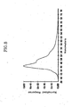
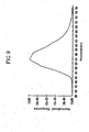
- Table 1 lists melting points and color of light emission of some exemplary double-spiro compounds of General Formula I.
- Table 1 Chemical Compound Nos. Melting Point (°C) Color of Light Emission 100 >500 Blue 102 >500 Blue 103 430 Blue 107 365.2 Blue 109 448 Blue 110 424.8 Blue 111 475.5 Blue 113 430.3 Blue 117 462.6 Blue 118 409.8 Blue 134 395.2 Blue 135 >500 Green 200 462.9 Blue 305 353 Blue 307 315.9 Blue 308 329.2 Blue 301 370.4 Blue 303 326.0 Blue 400 358.7 Blue 401 489.5 Blue 403 413.0 Blue
- the organic compounds of General Formula I have melting points sufficient to use in organic EL devices.
- the high melting point can be attributed, among other things, to the double-spiro structure with the fused six aromatic rings.
- these organic compounds have a melting point above about 300°C and glass transition temperature above about 120°C.
- the melting point is above about 400°C. Given the high melting point and high glass transition temperature, morphology changes or crystallization in the thin films of these organic compounds will be less likely. Therefore, the production yield and product stability of the organic EL devices will be substantially enhanced.
- the double-spiro organic compounds of General Formula 1 show good sublimability while at the same time the melting points thereof are sufficiently high.
- the sublimability of these compounds can be attributed to the structural rigidity as discussed above.
- each planar moiety in the compounds holds the two dimensional rigidity with its two fused phenyl rings; on the other hand, the whole double-spiro structure has the three dimensional rigidity by balancing the spatial location of the planar moieties.
- the aromatic phenyl units in the compounds can also add the sublimability as well.
- the steric hindrance effect of the substantially perpendicular configuration of each planar moiety makes the crystallinity of the compounds substantially lower than other compounds having the same or a similar number of conjugated double bond rings. If the steric hindrance effect of a compound is high, the melting point of the compound is generally low. In the compounds of General Formula 1, however, even if the steric hindrance effect exists, the high molecular weight keeps the melting point of the compounds sufficiently high, which prevents crystallization at a relatively low temperature.
- the double-spiro compounds of General Formula 1 have relatively low crystallinity while having high aromaticity owing to the existence of six fused phenyl rings.
- compounds having high aromaticity are of high crystallinity and easy to crystallize.
- the conjugation of double bonds in each of the six phenyl rings does not overlap with other phenyl rings in the double-spiro structure. More particularly, the conjugations in the two phenyl groups fused with the pentagonal or hexagonal ring in each planar moiety do not overlap with each other in that planar moiety.
- conjugation in either of the phenyl groups of each planar moiety does not overlap with conjugation in another planer moiety of the double-spiro structure. This means that even if each planar moiety is substituted with groups forming extended conjugation with its phenyl groups, the pi-orbital overlap in the conjugation would not extend over another planar moiety and accordingly the whole molecule either. The lack of overlap of conjugation explains the relatively low crystallinity of these compounds.
- Double-spiro compounds of General Formula 1 can be synthesized in various ways. For example, certain basic double-spiro compounds are first synthesized, and then they are modified to produce more complicated double-spiro compounds.
- the basic double-spiro compounds have one or more reactive atoms and/or functional groups as substituents in a double-spiro skeleton.
- the reactive atoms and/or functional groups are halogen atoms and any acidic leaving groups. More preferably, they are selected from the group of chlorine, bromine, iodine, p-toluenesulfonic acid, and trifluoroacetic acid.
- Some exemplary basic double-spiro molecules are listed below as Chemical Compounds 1-11. In these compounds, "Br" may be substituted with any other reactive atoms or functional groups.
- the basic double-spiro compounds are prepared in multi-step chemical reactions.
- certain precursor molecules are synthesized and further processed to produce basic double-spiro compounds.
- the precursor molecules include 2-bromo-9,10-bis(2-biphenyl-hydroxy)-anthracene and 2,6-dibromo-9,10-bis(2-biphenyl-dihydroxy)-anthracene.
- the basic double-spiro compounds are modified to produce desired double-spiro compounds.
- the modification of the basic double-spiro molecules is to introduce proper substituent groups into the double-spiro moiety of the basic molecules for favorable properties for use in organic electroluminescence. Reactions that can be used in such a modification includes, for example, Suzuki-coupling, Heck-coupling and Wittig reaction.
- the reactive atoms or functional groups of the basic molecules are subject to reaction with boronic acid or molecules having a boronate to produce a double-spiro compounds having a new substituent group.
- the reactive atoms or functional groups are reacted with compounds containing atoms for nucleophilic substitution, such as nitrogen and sulfur, to produce double-spiro compounds having substituent groups linked by a non-carbon atom.
- basic double-spiro molecules can be reacted with compounds containing vinyl groups to obtain double-spiro molecules substituted with olefinic groups.
- double-spiro molecules having olefinic substituent groups can be produced by reacting basic double-spiro molecules with compounds containing a carbonyl group such as an aldehyde under a Wittig reaction condition.
- a carbonyl group such as an aldehyde under a Wittig reaction condition.
- the synthesis of various double-spiro organic compounds will be further discussed in Examples 1-33.
- the present inventors have developed organic EL devices using organic compounds having one or more double-spiro structures. As discussed above, many double-spiro organic compounds have light-emitting property and other properties favorable for use in organic EL devices, including hole injection, hole transportation, electron transportation and electron injection. Various organic EL devices can be constructed with the double-spiro organic compounds of the present invention in combination with any other compounds having characteristics and properties for use in the organic EL devices. Further, some of the double-spiro organic compounds of the present invention have more than one function in the process of organic electroluminescence. With these multi-functional organic EL compounds, further various constructions of organic EL devices can be available.
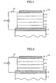
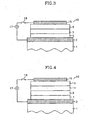
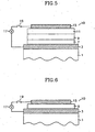
- FIG. 1-6 illustrate various examples of organic EL device constructions composed of a plurality of layers.
- the same reference numbers are used to indicate like components between the embodiments.
- the term "layer” in these illustrations refers to a thin film deposit of one or more compounds.
- the constructions of the organic EL device of the present invention include a substrate 1, an anode 3, a cathode 15 and one or more layers located between the anode 3 and the cathode 15, as illustrated in Figures 1-6 although not limited thereto.
- the one or more intervening layers contain at least one of the instant double-spiro organic compound.
- the double-spiro compounds contained in the one or more intervening layers satisfy General Formula 1.
- the one or more intervening layers include a hole-injecting layer 5, a hole-transporting layer 7, a light-emitting layer 9, an electron-transporting layer 11, an electron-injecting layer 13 and combinations of more than one of these layers.
- the substrate 1 ( Figures 1-6 ) supports the laminated structure of the organic EL device 10.
- the anode 3 ( Figures 1-6 ) and cathode 15 ( Figures 1-6 ) are electrically connected to an electric power source 17 ( Figures 1-6 ) via a switch 19 ( Figures 1-6 ), which is controlled by a controller (not shown).
- the hole-injecting layer 5 ( Figures 1-3 ) facilitates the injection of holes from the anode 3 into the hole-transporting layer 7 ( Figures 1-5 ).
- the electron-injecting layer 13 ( Figures 1 and 4 ) facilitates the injection of electrons from the cathode 15 into the electron-transporting layer 13.
- the hole-transporting layer 7 accelerates the movement of holes away from the anode 3 or hole-injecting layer 5 into, for example, the light-emitting layer 9 ( Figures 1-6 ).
- the electron-transporting layer 11 ( Figures 1, 2 , 4 and 5 ) accelerates the movement of electrons away from the cathode 15 or the electron-injecting layer 13 into, for example, the light-emitting layer 9 ( Figures 1-6 ).
- the transferred holes and electrons recombine and form excitons at light emitting molecules in the light-emitting layer 9.
- the excitons transfer the energy of the recombination to the light-emitting molecules or to other light-emitting molecules, which release the transferred energy in the form of visible light.
- the one or more intervening layers may be multi-functional.
- a multi-functional layer has functions of, for example, hole injection and transportation; electron injection and transportation; hole transportation and light emission; electron transportation and light emission; hole injection, hole transportation and light emission; electron injection, electron transportation and light emission; and so forth.
- Such multi-functional layers can be made of a material having multi-functional properties with or without doping of other functional materials. In the alternative such layers are made of a mixture of more than one material having different functional properties still with or without doping of other functional materials.
- the substrate 1 provides a support on which the laminated construction of the organic EL device can be build. Also, the substrate 1 functions as a protective layer for the construction of the organic EL device once manufactured. Thus, materials for the substrate 1 are selected from those which can stand the conditions of manufacturing processes and usage of the organic EL devices. In some organic EL device constructions of the present invention, the light emitted from the one or more intervening layers 5, 7, 9, 11 and 13 pass through the substrate 1. In such constructions, the substrate 1 is advantageously made of a transparent material to allow the visible light emitted from the light-emitting layer 9 to pass through. Transparent materials, which can be used for the substrate 1, for example, include glass, quartz and any other appropriate artificial materials such as transparent plastics.
- the substrate 1 is advantageously made of highly reflective material satisfying thermodynamic and mechanical requirements for depositing the anode 3 thereon.
- semiconductor wafers, metal oxide, ceramic materials, and non-transparent plastics can be used as the substrate 1.
- a transparent substrate coated with a reflective material can also be used.
- the anode 3 is a conductive electrode electrically connected to an electric power source.
- the anode 3 requires a relatively large work function, advantageously greater than 4 eV.
- conductive materials which can be used for the anode 3, include carbon; aluminum, vanadium, chromium, copper, zinc, silver, gold, similar metals, and alloys of the foregoing metals; zinc oxide, indium oxide, induim tin oxide (hereinafter referred to as "ITO"), indium zinc oxide and similar tin oxide or tin oxide indium-based complex compounds; mixtures of oxides and metals, such as ZnO:Al, SnO 2 :Sb; and conductive polymers, such as poly (3-methylthiophene), poly[3,4-(ethylene-1,2-dioxy) thiophene], polypyrrole and polyaniline.
- Either transparent or non-transparent materials can be selected for the anode 3, depending upon the construction of the light passage in the organic EL device as discussed above in connection with the materials for the substrate 1.
- the anode 3 is made of ITO.
- the anode 3 may be constructed in multiple layers of materials. The thickness of the anode 3 may vary depending on the materials used and its layered structures. However, the anode 3 is advantageously from about 10 nm to about 1000 nm, preferably from about 10 nm to about 500 nm.
- the cathode 15 requires a relatively small work function, advantageously smaller than 4 eV.
- conductive materials which can be used for the cathode 15, include magnesium, calcium, sodium, potassium, titanium, indium, yttrium, lithium, gadolinium, aluminum, silver, tin, lead, similar metals, and alloys of foregoing metals.
- the cathode 15 may be constructed in multiple layers of materials, such as LiF/Al and Li 2 O/Al.
- the cathode 15 is made of aluminum-lithium alloy, LiF/Al or Li 2 O/Al.
- Either transparent or non-transparent materials may be used for the cathode 3, depending upon the construction of the light passage in the organic EL device as discussed above.
- the thickness of the cathode 15 may vary depending on the materials used and its layered structures. However, the cathode 15 is laminated advantageously from about 1 nm to about 10,000 nm, preferably from about 5 nm to about 5,000 nm.
- the hole-injecting layer 5 has the function of enabling a large number of holes to be injected from the anode 3 at a low electric field applied to the device.
- the hole-injecting layer 5 advantageously is formed in the cases either where the interfacial strength between anode layer 3 and hole-transporting layer 7 is not strong enough or where the work function of the anode material is significantly different from the highest occupied molecular orbital (HOMO) level of the material of its neighboring layer 7, 9, 11 or 13.
- the HOMO level of the hole-injecting material is advantageously located between the work function of the anode 3 and the HOMO level of the other neighboring layer 9, 11 or 13, preferably near the middle of the two.
- the hole-injecting material is preferred to be transparent when the construction of the organic EL device allows the light emission through the substrate 1. In otherwise constructions, the hole-injecting material is advantageously non-transparent.
- the hole-injecting layer 5 can be made of one or more of the double-spiro structured compounds.
- the double-spiro compounds are of General Formula 1.
- the hole-injecting layer 5 includes one or more of the Chemical Compounds 300-308 and 400-413, most preferably, Chemical Compounds 300-308.
- one or more non-double-spiro hole-injecting materials may be added.
- the hole-injecting layer 5 can be formed with one or more non-double-spiro hole-injecting materials as long as at least one double-spiro compound is used in the organic EL device.
- the non-double-spiro hole-injecting materials include, for example, metal porphyrine ( U.S. Patent Nos. 4,720,432 and 4,356,429 ); oligothiophene ( U.S. Patent No. 5,540,999 ); arylamines and derivatives thereof ( U.S. Patent Nos. 5,256,945 , 5,609,970 , and 6,074,734 , and Japanese Unexamined Patent Publications 1999-219788 and 1996-269445 ); hexanitrile hexaazatriphenylene; conductive polymers such as derivatives of polyaniline, polythiophene with or without acid dopant; derivatives of quinacridone; derivatives of perylene ( U.S. Patent No. 5,998,803 ); and anthraquinone ( Japanese Unexamined Patent Publication 2000-058267 .).
- metal porphyrine U.S. Patent Nos. 4,720,432 and 4,356,429
- the hole-transporting layer 7 has the function to smoothly transfer the holes from the hole-injecting layer 5 or from anode 3 (in the absence of the hole-injecting layer 5) toward the light-emitting layer 9 or toward an area where light-emitting materials are doped. Materials good for use in the hole-transporting layer 7 are those having high hole mobility therein.
- This hole-transporting layer 7 also has the function of blocking electrons from its neighboring layer 9, 11, or 13 on the side of the cathode 15. Further, the hole-transporting layer 7 functions for both the hole injection and hole transportation in the constructions which do not have a separate hole-injecting layer.
- the hole-transporting layer 7 can be made of one or more of the double-spiro structured compounds.
- the double-spiro compounds are preferably of General Formula 1. More preferably, the hole-transporting layer 7 includes one or more of the Chemical Compounds 300-308 and 400-413.
- one or more non-double-spiro hole-transporting materials may be added.
- the hole-transporting layer 7 can be formed with one or more non-double-spiro hole-transporting materials as long as at least one double-spiro compound is used in the organic EL device.
- the non-double-spiro hole-transporting materials include, for example, arylamine derivatives, conjugated poylmers, block co-polymers with conjugated and nonconjugated repeating units, and the like.
- derivatives of the arylamine, 4,4'-bis[N-(1-naphthyl)-N-phenylamino]biphenyl (NPB) is used for the hole-transporting layer 7.
- the electron-transporting layer 11 contains an electron transfer material to transfer the electron injected from the electron injecting layer 13 or from the cathode 15 (in the absence of the electron-injecting layer 13) to the light-emitting layer 9 or to an area where a light-emitting material is doped. Compounds having high electron mobility is used as an electron-transporting material.
- the electron-transporting layer 11 may also have the function of blocking holes to move thereinto. In the construction without a separate electron-injecting layer, the electron-transporting material is selected from those which can enable a large number of electron to be injected from the cathode 15 at a low electric field applied across the device.
- the electron-transporting layer 11 can be made of one or more of the double-spiro structured compounds.
- the double-spiro compounds are of General Formula 1.
- the electron-transporting layer 11 includes one or more of the Chemical Compounds 200-222.
- one or more non-double-spiro electron-transporting materials may be added.
- the electron-transporting layer 11 can be formed with one or more non-double-spiro electron-transporting materials as long as at least one double-spiro compound is used in the organic EL device.
- the non-double-spiro electron-transporting materials include, for example, aluminum complexes of 8-hydroxyquinoline; organometallic complex compounds including Alq3 ( U.S. Patent No. 5,061,569 and U.S. Patent Application No. 09/540837 ); organic radical compounds ( U.S. Patent No. 5,811,833 ); hydroxyflavon-metal complexes ( U.S. Patent Nos. 5,817,431 and 5,516,577 , Japanese Unexamined Patent Publications 2001-076879 , 2001-123157 and 1998-017860 , and Organic Light-emitting Diodes using 3- or 5-hydroxyflavone-metal Complexes, Appl. Phys. Lett. 71 (23), 3338 (1997 ))..
- the electron-injecting layer 13 is generally to faciliate injection of a large number of electrons from the cathode 15 at a low electric field applied across the device.
- the electron-injecting layer 13 is provided when the work function of the cathode 15 significantly differs from the lowest unoccupied molecular orbital (LUMO) level of the other neighboring layer 5, 7, 9 or 11.
- the electron-injecting layer 13 may be introduced to prevent excitons generated in the neighboring layer 5, 7, 9 or 11 from moving toward the cathode layer 15.
- the electron-injecting layer 13 may be provided to avoid damaging the neighboring layer 5, 7, 9 or 11 in the course of the deposition of the cathode layer 15.
- the LUMO level of the electron-injecting material is advantageously located between the work function of the cathode material and the LUMO level of the other neighboring layer 5, 7, 9 or 11, preferably near the middle of the two. Further, the electron-injecting layer 13 is required to have strong interface with the cathode layer 15.
- the electron-injecting layer 13 can be made of one or more of the double-spiro structured compounds.
- the double-spiro compounds are of General Formula 1.
- the electron-injecting layer 13 includes one or more of the Chemical Compounds 200-222.
- one or more non-double-spiro electron-injecting materials may be added.
- the electron-injecting layer 13 can be formed with one or more non-double-spiro electron-injecting materials as long as at least one double-spiro compound is used in the organic EL device.
- the non-double-spiro electron-injecting materials include, for example, aluminum complexes of 8-hydroxyquinoline, organometallic complex compounds including Alq3, organic radical compounds ( U.S. Patent No. 5,811,833 ); 3- or 5-hydroxyflavone-metal complexes (Organic Light-emitting Diodes using 3- or 5-hydroxyflavone-metal Complexes, Appl. Phys. Lett.
- the light-emitting layer 9 is a layer particularly dedicated to the emission of visible light by the process of recombination of electrons and holes therein although it may have other functions as well.
- the light-emitting layer 9 of the organic EL devices is composed of one light-emitting material alone or a mixture of two or more light-emitting materials without doping.
- the light-emitting layer 9 is composed of one or more light-emitting host materials and a small amount of one or more dopants, as will be discussed below.
- the light-emitting layer 9 can include one or more of the instant double-spiro structured compounds.
- the double-spiro compounds are of General Formula 1 as a light-emitting material.
- the light-emitting layer 9 includes one or more of the Chemical Compounds 100-137, 200-222, and 400-413.
- these double-spiro compounds can be used as a host or as a dopant. In either case, one or more non-double-spiro light-emitting materials may be added as either another host material or another dopant.
- the double-spiro compounds are used as a host material, with or without another host material, for hosting one or more fluorescent or phosphorescent dopants.
- the light-emitting layer 9 may include one or more non-double-spiro light-emitting materials as long as at least one double-spiro compound is used in the organic EL device.
- the non-double-spiro light-emitting materials include, for example, 8-hydroxyquinoline metal complexes including Alq3; carbazole compounds and derivatives thereof; dimerized styryl compounds (U.S Patent No. 5,366,811 ); BAlq ( U.S.
- Patent No 5,150,006 10-hydroxybenzo [h] quinoline-metal complexes
- U.S. Patent No. 5,529,853 2-(2'-hydroxy-5'methylphenyl) benzotriazole metal complexes
- U.S. Patent No. 5,486,406 benzoxazole, benzthiazole, benzimidazole and derivatives thereof
- the light-emitting layer 9 may be constructed with or without a dopant. Dopants are introduced to improve the light-emission efficiency, to tune the color of the emission, and/or to simply emit light from a layer having a non-fluorescent host. Dopants can be added to the light-emitting layer 9 and one or more of the other layers 5, 7, 11 and 13. More than one light-emitting material can be doped together in these layers for various purposes. Also, in some constructions of the organic EL devices according to the present invention, the light-emitting layer 9 may be absent. In such constructions, one or more light-emitting dopants are necessarily put in one or more of the layers 5, 7, 11 or 13 to generate visible light therefrom.
- dopants are selected from fluorescent or phosphorescent materials having higher quantum efficiency than the host material.
- the dopants have a quantum yield close to "1" in a dilute system. This means that most of the energy received from excitons contributes to the light emission rather than releasing it in other forms such as generating heat.
- dopants are selected such that they match energetically with the host material. In other words, excitons are known to have a tendency to transfer their energy to a material having a smaller band gap among materials near the recombination location; thus, dopants are advantageously selected from the light-emitting materials having a band gap slightly smaller than that of the host materials.
- recombination may occur in the host molecules, and the energy of the generated excitons is transferred to the dopants. In this case, visible light is emitted from the dopant molecules. Also, the energy of the excitons may be transferred to another dopant, where the light is emitted. In the alternative, the recombination and light emission may occur in one light-emitting material.
- the double-spiro light-emitting compounds can be used as a dopant in various layers.
- these dopants have the double-spiro structure of General Formula 1.
- Chemical Compounds 100-137, 200-222 and 400-413 can be used as a dopant light-emitting material.
- One or more double-spiro dopants can be used with or without other dopants. Whether or not a separate light-emitting layer is provided, quantum efficiency and lifetime of the organic EL device can be enhanced by selecting an appropriate host materials, one or more matching dopants and their concentrations.
- light-emitting (phosphorescent or fluorescent) materials for doping in the organic EL devices of the present invention include, for example, perylene, rubrene, coumarine, quinacridone, nile red, DCM, and the following organometallic complexes.
- 2-bromo-9,10-bis(2-biphenyl-dihydroxy)-anthracene 9.50 g (16.0 mmol) of 2-bromo-9,10-bis(2-biphenyl-hydroxy)-anthracene synthesized as above was suspended in acetic acid (150 ml), and conc. H 2 SO 4 (20 drops) was added thereto. After the reaction mixture had been stirred at reflux for about 3 hours, it was cooled to room temperature. The precipitate was filtered off with suction, washed with acetic acid, water, and ethanol.
- anthraquinone-2-aldehyde diacetate (16.0 g, 65%.)
- acetic acid 400 ml
- 35% aqueous hydrochloric acid 170 ml
- the reaction mixture had been stirred while refluxing for 15 min, cooled to room temperature, filtered off with suction, and washed with water. After drying, anthraquinone-2-aldehyde (10.0 g, 89%) was obtained.
- Chemical Compound 7 (0.97 g, 1.20 mmol) was prepared by reacting Chemical Compound 11 and N -bromosuccinimide in carbon tetrachloride, diphenylamine (0.61 g, 3.60 mmol), and sodium tert -butoxide (0.28 g, 2.40 mmol). To a suspension of Chemical Compound 7 in xylene (20 ml), palladium acetate (12 mg, 0.05 mmol) and tri- tert -butylphosphine (39 mg, 0.20 mmol) were added.
- a glass substrate coated with a thin film of ITO (indium tin oxide) having thickness of about 1500 ⁇ was ultrasonically cleaned in a solution of a cleaning agent, dried, and transferred into a plasma cleaning device.
- the substrate was cleaned with oxygen plasma for 5 minutes, and transferred to a thermal vapor deposition chamber.
- a hole-injecting layer having thickness of about 500 ⁇ was formed by thermal vacuum deposition of the hexanitrile hexaazatriphenylene, a stable hole-injecting material, over the ITO (anode).
- a hole-transporting layer having thickness of about 600 ⁇ was formed by thermal vacuum deposition of NPB, a hole-transporting material, over the hole-injecting layer.
- An emitting layer having thickness of about 150 ⁇ was formed by thermally vacuum depositing Chemical Compound 12 over the hole-transporting layer.
- 8-hydroxyquinoline Aluminum salt (Alq3) an n-type organic semiconductor, was deposited with thickness of about 300 ⁇ to form an electron-transporting layer.
- a cathode electrode was formed by depositing 5 ⁇ of LiF and about 2500 ⁇ of aluminum on the electron-transporting layer. In the process, the deposition speed was controlled to maintain 1 ⁇ /sec for organic material, 0.2 ⁇ /sec for lithium fluoride, and 3-7 ⁇ /sec for aluminum.
- An organic light-emitting device was produced in the same manner as in Comparative Example A except that Chemical Compound 109 was used as the light-emitting material with thickness of about 400 ⁇ instead of Chemical Compound 12.
- forward bias was applied across the light-emitting device, blue light emission centered at the wavelength of 452 nm was observed.
- the efficiency of the light-emitting device was 2.0 cd/A at a current density of 10 mA/cm 2 .
- An organic light-emitting device was produced in the same manner as in Comparative Example A except that Chemical Compound 102 was used as the light-emitting material with thickness of about 400 ⁇ instead of Chemical Compound 12.
- forward bias was applied across the light-emitting device, blue light emission centered at the wavelength of 464 nm was observed.
- the efficiency of the light-emitting device was 2.5 cd/A at a current density of 10 mA/cm 2 .
- An organic light-emitting device was produced in the same manner as in Comparative Example A except that Chemical Compound 118 was used as the light-emitting material with thickness of 300 ⁇ instead of Chemical Compound 12.
- forward bias was applied across the light-emitting device, blue light emission centered at the wavelength of 464 nm was observed.
- the efficiency of the light-emitting device was 2.1 cd/A at a current density of 10 mA/cm 2 .
- An organic light-emitting device was produced in the same manner as in Comparative Example A except that Chemical Compound 100 was used as the light-emitting material with thickness of about 300 ⁇ instead of Chemical Compound 12.
- forward bias was applied across the light-emitting device, blue light emission centered at the wavelength of 444 nm was observed.
- the efficiency of the light-emitting device was 0.64 cd/A at a current density of 10 mA/cm 2 .
- An organic light-emitting device was produced in the same manner as in Comparative Example A except that Chemical Compound 117 was used as the light-emitting material with thickness of about 150 ⁇ instead of Chemical Compound 12.
- forward bias was applied across the light-emitting device, blue light emission centered at the wavelength of 484 nm was observed.
- the efficiency of the light-emitting device was 2.4 cd/A at a current density of 10 mA/cm 2 .
- An organic light-emitting device was produced in the same manner as in Comparative Example A except that Chemical Compound 113 was used as the light-emitting material with thickness of about 150 ⁇ instead of Chemical Compound 12.
- forward bias was applied across the light-emitting device, blue light emission centered at the wavelength of 452 nm from the compound having a structure of Chemical Compound 113 was observed.
- the efficiency of the light-emitting device was 1.6 cd/A at a current density of 10 mA/cm 2 .
- An organic light-emitting device was produced in the same manner as in Comparative Example A except that Chemical Compound 111 was used as the light-emitting material with thickness of 150 ⁇ instead of Chemical Compound 12.
- forward bias was applied across the light-emitting device, blue light emission centered at the wavelength of 452 nm was observed.
- the efficiency of the light-emitting device was 2.1 cd/A at a current density of 10 mA/cm 2 .
- An organic light-emitting device was produced in the same manner as in Comparative Example A except that Chemical Compound 110 was used as the light-emitting material with thickness of 150 ⁇ instead of Chemical Compound 12.
- When forward bias was applied across the light-emitting device blue light emission centered at the wavelength of 440 nm was observed.
- the efficiency of the light-emitting device was 1.9 cd/A at a current density of 10 mA/cm 2 .
- Figure 7 shows the spectrum of light emission of this device.
- An organic light-emitting device was produced in the same manner as in Comparative Example A except that Chemical Compound 134 was used as the light-emitting material with thickness of 300 ⁇ instead of Chemical Compound 12.
- forward bias was applied across the light-emitting device, green light emission centered at the wavelength of 508 nm was observed.
- the efficiency of the light-emitting device was 1.3 cd/A at a current density of 10 mA/cm 2 .
- An organic light-emitting device having the construction as illustrated in Figure 2 was manufactured, in which Chemical Compound 200 was used as an electron-tiansporting material.
- a glass substrate coated with a thin film of ITO (indium tin oxide) having thickness of about 1500 ⁇ was ultrasonically cleaned in a solution of a cleaning agent, dried, and transferred into a plasma cleaning device. The substrate was cleaned with oxygen plasma for 5 minutes, and transferred to a thermal vapor deposition chamber.
- a hole-injecting layer having thickness of about 500 ⁇ was formed by thermal vacuum deposition of hexanitrile hexaazatriphenylene over the ITO coating (anode).
- a hole-transporting layer having thickness of about 600 ⁇ was formed by thermal vacuum deposition of NPB over the hole-injecting layer.
- An emitting layer having thickness of about 150 ⁇ was formed by thermal vacuum deposition of Chemical Compound 117.
- Chemical Compound 200 was deposited under vacuum with thickness of about 300 ⁇ to form an electron-transporting layer. Then, an cathode electrode was formed by depositing 5 ⁇ of LiF and about 2500 ⁇ of aluminum on the electron-transporting layer. In the process, the deposing speed was controlled to maintain 1 ⁇ /sec for organic material, 0.2 ⁇ /sec for lithium fluoride, and 3-7 ⁇ /sec for aluminum.
- An organic light-emitting device having the construction as illustrated in Figure 2 was manufactured, using Chemical Compound 110 as a host light-emitting molecule and tetra t-butyl perylene as a dopant molecule.
- a glass substrate coated with a thin film of ITO (indium tin oxide) having thickness of about 1500 ⁇ was ultrasonically cleaned in a solution of a cleaning agent, dried, and transferred into a plasma cleaning device.
- the substrate was cleaned with oxygen plasma for 5 minutes, and transferred to a thermal vapor deposition chamber.
- a hole-injecting layer having thickness of about 500 ⁇ was formed by thermal vacuum deposition of hexanitrile hexaazatriphenylene over the ITO (anode).
- a hole-transporting layer having thickness of about 600 ⁇ was formed by thermal vacuum deposition of NPB over the hole-injecting layer.
- An emitting layer having thickness of about 150 ⁇ was formed by co-deposition of Chemical Compound 110 and 1 wt% of tetra t-butyl perylene.
- 8-hydroxyquinoline Aluminum salt (Alq3) was deposited with a thickness of about 300 ⁇ to form an electron-transporting layer.
- a cathode electrode was formed by depositing 5 ⁇ of LiF and about 2500 ⁇ of aluminum on the electron-transporting layer.
- the deposing speed was controlled to maintain 3 ⁇ /sec for the host material and 0.2 ⁇ /sec for lithium fluoride, and 3-7 ⁇ /sec for aluminum.
- An organic light-emitting device having the construction as illustrated in Figure 2 was manufactured, using Chemical Compound 110 as a host light-emitting molecule and DSA amine as a dopant molecule.
- the organic light-emitting device was obtained in the same manner as in Example 45 except that the thickness of the emitting layer was about 300 ⁇ and DSA amine was used codeposited with Chemical Compound 110 as a dopant material instead of tetra t-butyl perylene.
- forward bias was applied across the light-emitting device, blue light emission centered at the wavelength of 460 nm was observed.
- the efficiency of the light-emitting device was 4.6 cd/A at a current density of 10 mA/cm 2 .
- An organic light-emitting device having the construction shown in Figure 3 was manufactured, using Chemical Compound 301 as a hole-transporting material.
- a glass substrate coated with a thin film of ITO (indium tin oxide) having thickness of about 1500 ⁇ was ultrasonically cleaned in a solution of a cleaning agent, dried, and transferred into a plasma cleaning device. The substrate was cleaned with oxygen plasma for 5 minutes, and transferred to a thermal vapor deposition chamber.
- a hole-injecting layer having thickness of about 500 ⁇ was formed by thermal vacuum deposition of hexanitrile hexaazatriphenylene over the ITO coating (anode).
- a hole-transporting layer having thickness of about 400 ⁇ was formed by thermal vacuum deposition of Chemical Compound 301 over the hole-injecting layer.
- Alq3 8-hydroxyquinoline Aluminum salt
- an cathode electrode was formed by depositing 5 ⁇ of LiF and about 2500 ⁇ of aluminum on the electron-transporting layer.
- the deposing speed was controlled to maintain 1 ⁇ /sec for organic material, 0.2 ⁇ /sec for lithium fluoride, and 3-7 ⁇ /sec for aluminum.
- An organic light-emitting device was obtained in the same manner as in Example 46 except that Chemical Compound 400 was used as a hole-transporting material instead of Chemical Compound 301.
- When forward bias was applied across the light-emitting device green light emission from the Alq3 centered at the wavelength of 536 nm was observed.
- the efficiency of the light-emitting device was 3.4 cd/A at a current density of 10 mA/cm 2 .
- An organic light-emitting device was obtained in the same manner as in Example 46 except that Chemical Compound 303 was used as a hole-transporting material instead of Chemical Compound 301.
- When forward bias was applied across the light-emitting device green light emission from the Alq3 centered at the wavelength of 536 nm was observed.
- the efficiency of the light-emitting device was 4.3 cd/A at a current density of 10 mA/cm 2 .
- An organic light-emitting device was obtained in the same manner as in Example 46 except that Chemical Compound 403 was used as a hole-transporting material instead of Chemical Compound 301.
- When forward bias was applied across the light-emitting device green light emission from the Alq3 centered at the wavelength of 540 nm was observed.
- the efficiency of the light-emitting device was 3.7 cd/A at a current density of 10 mA/cm 2 .
- An organic light-emitting device was obtained in the same manner as in Example 46 except that Chemical Compound 305 was used as a hole-transporting material instead of Chemical Compound 301.
- When forward bias was applied across the light-emitting device green light emission from the Alq3 centered at the wavelength of 540 nm was observed.
- the efficiency of the light-emitting device was 4.8 cd/A at a current density of 10 mA/cm 2 .
- Figure 9 illustrates the light-emission spectrum of this device.
- Chemical Compound 305 used in the hole-transporting layer 7 has the band gap corresponding to blue light emission. Because the emitted light is green, not blue, Chemical Compound 305 is assumed to transport holes from the hole-injecting layer 5 to the light-emitting layer 9, rather than emitting light from itself.
- An organic light-emitting device was obtained in the same manner as in Example 46 except that Chemical Compound 308 was used as a hole-transporting material instead of Chemical Compound 301.
- When forward bias was applied across the light-emitting device green light emission from the Alq3 centered at the wavelength of 540 nm was observed.
- the efficiency of the light-emitting device was 2.3 cd/A at a current density of 10 mA/cm 2 .
Landscapes
- Chemical & Material Sciences (AREA)
- Organic Chemistry (AREA)
- Engineering & Computer Science (AREA)
- Materials Engineering (AREA)
- Physics & Mathematics (AREA)
- Spectroscopy & Molecular Physics (AREA)
- Chemical Kinetics & Catalysis (AREA)
- Electroluminescent Light Sources (AREA)
- Indole Compounds (AREA)
- Organic Low-Molecular-Weight Compounds And Preparation Thereof (AREA)
- Heterocyclic Carbon Compounds Containing A Hetero Ring Having Oxygen Or Sulfur (AREA)
Abstract
Description
- The present invention generally relates to organic electroluminescence. More particularly, the present invention pertains to organic EL device using novel organic compounds having electroluminescent (hereinafter referred to as "EL") characteristics.
- Organic electroluminescence is one of the instances in which electric current is converted into visible light by internal processes of certain organic molecules. Organic molecules having either fluorescent or phosphorescent characteristics generate light emission upon the application of electric current, although they differ in their internal processes and response time. Both organic fluorescent and phosphorescent molecules are referred to as organic EL or light-emitting molecules.
- The organic EL technology has been used in luminescent displays which produce their own light, unlike liquid crystal displays, which require an independent light source. Various colors can be generated by using an individual color-generating compound or combining compounds generating basic color elements. This technology is advantageous over LCD technology in its low power consumption, faster response time, higher brightness level, unlimited viewing angle and thinner design.
- A basic construction of an organic EL device includes two opposing electrodes, i.e., a cathode and an anode, and an intervening layer containing an organic light-emitting material. When applying an electric voltage between the electrodes, electrons and holes are injected from the cathode and anode, respectively, into the intervening layer. The holes and electrons recombine at organic light-emitting molecules in the intervening layer. Recombined pairs of electrons and holes, namely excitons, move around carrying the energy generated by the recombination and transfer the energy to other organic light-emitting molecules, particularly to those having a smaller band gap near the location of their recombination. The transferred energy is used to excite valence electrons of the organic light-emitting molecules, which generates photons when the electrons return to their ground state.
- In order to improve energy efficiency, multiple-layered organic EL devices have been suggested. Generally, multiple-layered organic EL devices have one or more layers functioning as vehicles for hole injection, hole transportation, light emission, electron transportation, and electron injection. One or more layers of the multiple-layered constructions may have more than one function. Many organic compounds have been known to have physical properties and characteristics for use in such organic EL devices. However, there exists a need for new organic compounds for use in organic electroluminescence in order to improve various aspects of organic EL devices or the manufacture of such devices.
- Documents
WO 98/42655 A EP-A-0 676 461 andEP-A-0 707 020 describe organic electroluminescent devices comprising a light emitting layer or a charge injecting/charge transporting layer comprising a 9,9'-spirobifluorene derivative. - One aspect of the present invention provides organic EL devices comprising an anode, a cathode, and at least one solid deposition located between the anode and the cathode, wherein the solid deposition comprises at least one light-emitting layer having a double-spiro compound of Chemical Formula I:

- The chemical compound of General Formula 1 is selected from the group consisting of Chemical Compounds 1-11, 100-137, 200-222, 300-308, and 400-413 as will be shown later. The compound has a melting point above about 300 °C. The compound has a band-gap corresponding to visible light emission. The band-gap for the visible light emission is from about 1.8 eV to about 3.5 eV. The band-gap corresponds to blue, green or red light emission. The compound has a hole-transporting property. Hole mobility in the compound is about 1x10⁻⁷ cm2/Vs or greater. The compound has an electron-transporting property. Electron mobility in the compound is about 1x10⁻⁷ cm2/Vs or greater. The compound has a hole-injecting property. The compound has the highest occupied molecular orbital (HOMO) level from about -4.0 eV to about -6.0 eV. The compound has an electron-injecting property. The compound has the lowest unoccupied molecular orbital (LUMO) level from about -2.5 eV to about -4.0 eV.
- The chemical compounds comprise one or more double-spiro compounds, wherein the double-spiro compounds comprise at least three substantially planar organic moieties configured such that one planar moiety is interveningly located between the other two planar moieties and that the at least three planar moieties have substantially no overlap with one another; wherein the intervening planar moiety shares an atom with each of the two neighboring planar moieties; wherein the intervening planar moiety is substantially perpendicular to the two neighboring planar moieties; wherein the at least three planar moieties may be the same or different from each other; and wherein each of the planar moiety may be substituted with one or more non-planar moieties.
- In the solid deposition, one or more double-spiro chemical compounds are in an amorphous form. The one or more chemical compounds further comprise one or more non-double-spiro compounds acceptable in organic electroluminescence. The one or more non-double-spiro compounds comprise a light-emitting compound. The non-double-spiro light-emitting compound has the band gap smaller than the band gap of the double-spiro compound. The non-double-spiro light-emitting compound has the band gap greater than the band gap of the double-spiro compound. The non-double-spiro light-emitting compound is either fluorescent or phosphorescent compound. The solid deposition is in the form of a thin film. The solid deposition comprises one or more layers. The double-spiro compound has one or more properties selected from the group consisting of visible light emission, electron transportation, electron injection, hole transportation, and hole injection.
- In the double-spiro compounds, the atoms shared with the neighboring planar moieties are apart from each other in the intervening planar moieties. Two or more rings constitute at least one of the substantially planar moieties, and wherein the two or more rings are fused by sharing two or more atoms to form a substantially rigid plane. Each planar moiety is isolated from conjugation with its neighboring planar moieties. One or more of the planar moieties comprises a C3-C7 ring fused with one or more C4-C7 aromatic rings, and wherein one or more carbon atoms in the rings can be replaced by a heteroatom. One or more of the planar moieties comprises a C5-C6 ring fused with one or more C5-C6 aromatic rings, and wherein one or more carbon atoms in the rings can be replaced by a heteroatom. One or more of the planar moieties are selected from the group consisting of the following organic moieties:


- The double-spiro compound has a melting point above about 300 °C. The double-spiro compound satisfies Chemical Formula I. In General Formula I, the R1 through R24 are one or more substituents selected from the group consisting of hydrogen atom, halogen atoms, substituted or unsubstituted alkyl groups having 1 to 18 carbon atoms, substituted or unsubstituted aryl groups having 6 to 24 carbon atoms, alkoxyl groups having 1 to 18 carbon atoms, substituted or unsubstituted heterocyclic or heteroaryl groups, substituted vinyl groups, amino group, amine groups, nitrile groups, nitro groups, formyl group, alkanoyl groups, substituted or unsubstituted carbazoles, alkyl sulfide groups, and aryl sulfide groups. The double-spiro compound are selected from the group consisting of Chemical Compounds 1-12, 100-137, 200-222, 300-308, and 400-413.
- The one or more double-spiro compounds have a band gap corresponding to visible light emission. The band-gap for the visible light emission is from about 1.8 eV to about 3.5 eV. The band-gap corresponds to blue, green or red light emission. The double-spiro compounds have a hole-transporting property. Hole mobility in the one or more double-spiro compounds is about 1x10⁻⁷ cm2/Vs or greater. The double-spiro compounds have a electron-transporting property. Electron mobility in the one or more double-spiro compounds is about 1x10⁻⁷ cm2/Vs or greater. The double-spiro compounds have a hole-injecting property. The double-spiro compounds have the highest occupied molecular orbital (HOMO) level from about -4.0 eV to about 6.0 eV. The double-spiro compounds have a electron-injecting property. The double-spiro compounds has the lowest unoccupied molecular orbital (LUMO) level from about -2.5 eV to about 4.0 eV.
- A method of making the discussed solid deposition comprises providing a support and depositing one or more chemical compounds comprising one or more of the double-spiro compounds. The deposition of one or more chemical compounds comprises physical vapor deposition. Also, the deposition of one or more chemical compounds comprises forming multiple layers of different compositions of the one or more chemical compounds.
- The light-emitting layer comprises the one or more double-spiro compounds having the band gap corresponding to visible light emission. The band-gap for the visible light emission is from about 1.8 eV to about 3.5 eV. The light-emitting layer comprises one or more fluorescent or phosphorescent materials. The organic EL device is supported by a substrate, and wherein the substrate contacts either the anode or the cathode. The one or more layers comprise at least one material having one or more properties selected from the group consisting of electron injection, electron transportation, light emission, hole transportation, and hole injection. The light-emitting layer comprises one or more compounds selected from the group consisting of Chemical Compounds 100-137, 200-222, and 400-413. The light-emitting layer further comprises one or more non-double-spiro light-emitting compounds. The non-double-spiro light-emitting compound has the band gap smaller than the band gap of the double-spiro compound. The non-double-spiro light-emitting compound has the band gap greater than the band gap of the double-spiro compound. The non-double-spiro light-emitting compound is either fluorescent or phosphorescent compound. The one or more layers comprise at least one of the electron-injecting and electron-transporting layers. The at least one of the electron-injecting and electron-transporting layers comprises Chemical Compounds 200-222. The one or more layers comprise at least one of the hole-injecting and hole-transporting layers. The at least one of the hole-injecting and hole-transporting layers comprises Chemical Compounds 300-308 and 400-413.
- Another aspect of the present invention provides an electronic device comprising a display, wherein the display comprises the organic EL device as discussed.
- The organic EL device is capable of generating visible light when electric power is applied between the anode and cathode of the device; the cathode injecting electrons toward the light-emitting layer; the anode injecting holes toward the light-emitting layer; and allowing recombination of at least part of the injected electrons and holes in the light-emitting layer, thereby generating visible light from the light-emitting layer. The light-emitting layer comprises the one or more double-spiro compounds having a light-emitting property. The light-emitting layer further comprises one or more non-double-spiro light-emitting compounds. The one or more layers comprises the double-spiro compound having one or more properties selected from the group consisting of visible light emission, electron transportation, electron injection, hole transportation, and hole injection.
- The organic EL device may be manufactured by a method comprising: providing a substrate; forming a first conductive layer; depositing the one or more chemical compounds comprising one or more of the double-spiro compounds so as to form the solid deposition comprising the light-emitting layer; and forming a second conductive layer, wherein either of the first and second conductive layers corresponds to the anode or cathode. The formation of the light-emitting layer comprises depositing one or more of the double-spiro compounds having a light-emitting property. The formation of the light-emitting layer comprises co-depositing one or more non-double-spiro light-emitting compounds. The deposition of the one or more chemical compounds further comprises forming layers having one or more functions selected from the group consisting of visible light emission, electron transportation, electron injection, hole transportation, and hole injection. The formation of the layers having one or more functions comprises depositing one or more of the double-spiro compounds. The formation of the layers having one or more functions comprises depositing one or more non-double-spiro compounds.
-
Figures 1-6 illustrate simplified cross-sectional views of various exemplary constructions of organic EL devices in accordance with the present invention. -
Figure 7 is a spectrum of light emission from the organic EL device manufactured in Example 41. -
Figure 8 is a spectrum of light emission from the Organic EL device manufactured in Example 44. -
Figure 9 is a spectrum of light emission from the organic EL device manufactured in Example 50. - Now the various aspects of the present invention will be discussed in more detail. It is to be understood at the outset of the description, which follows that persons of skill in the appropriate arts may modify the invention here describe while still achieving the favorable results of this invention. Accordingly, the following description is to be understood as being a broad, teaching disclosure directed to persons of skill in the appropriate arts, and not as limiting upon the present invention.
- The present inventors have invented a group of new organic EL compounds. In the course of the research for new organic EL compounds, the inventors considered various factors relating to the applicability of chemical compounds to the manufacturing of organic EL devices. These factors include, among other things, electroluminescence of candidate chemical compounds, sublimability of the compounds under given manufacturing conditions, thermal stability of thin film made of the compounds, etc.
- The electroluminescence of compounds is preferred although it is not always necessary for compounds to be used in organic EL devices. In order for an organic compound to generate visible light or to host another light-emitting compound, however, the organic compound needs to have its own electroluminescence. Although certain organic EL compounds have common functional groups or structural similarities, there is not a general rule as to what structures or elements of organic compounds would secure electroluminescence. Thus, it is difficult to find completely new structured organic EL compounds.
- Not only must the compounds electroluminesce, but their colors of emission and efficiency of electroluminescence are also important. The colors and efficiency are considered with other properties of the compounds in determining what functions the organic EL compound can do in organic EL devices. For example, a compound emitting blue color alone may form a layer emitting blue light. Also, the blue light-emitting compound can be used as a blue light-emitting dopant or as a host material for hosting various light-emitting dopants in a full color display. Also, efficiency of electroluminescence may be relevant to the consideration of whether the compound is to be used as a host or a dopant.
- Thermal stability of organic EL devices is a very important consideration. Quality of organic EL devices may deteriorate, as they happen to be subject to a high temperature, for example in a car heated by sunlight. Generally, organic EL devices have organic compounds in the form of amorphous thin films. The amorphous form of the compounds may crystallize when the temperature goes up above the glass transition temperature of the compounds. Even partial crystallization of the compounds may cause an electrical short between electrodes and result in the loss of electroluminescence. Crystallization in the amorphous films may also occur during the manufacturing process because it involves a high temperature. If crystallization occurs during the manufacturing, the very new products may have defects in the electroluminescence.
- In order to avoid thermal crystallization of organic compounds, the glass transition temperature of the compounds must be higher than a temperature to which the deposited thin film can possibly be subjected. Generally, organic EL compounds having a glass transition temperature of about 120°C or above are sufficient for use in organic EL devices. As glass transition temperature of a compound has good correlation with the melting point thereof, melting point is often used as a reference instead of glass transition temperature. The relationship between melting point and glass transition temperature is set forth in Molecular Design for Nonpolymeric Organic Dye Glasses with Thermal Stability, J. Phys. Chem. 97, 6240-6248 (1993), which is hereby incorporated herein by reference.
- Also, crystallinity of the organic compounds is relevant to the crystallization of organic EL compounds in thin films and therefore the stability of the organic EL devices. The crystallinity of a compound may be defined as the degree of crystallization or its tendency to crystallize. When an organic compound has high crystallinity, it is more likely to crystallize under a given condition than others having low crystallinity. Accordingly, organic compounds having low crystallinity are preferred. It has been found that organic molecules having high planarity and rigidity tend to crystallize, regardless of their melting points or substrate temperature, when thin-films thereof are formed on a substrate either by solution processing or physical vapor deposition.
- Further, organic EL compounds need to have good sublimability in view of the use of physical vapor deposition (PVD) in the formation of amorphous thin films. However, organic EL compounds with a high melting point generally have a large molecular weight and a poor sublimability. In fact, what is sought are organic EL compounds having high sublimability while having a sufficiently high melting point. Flat structures such as aromatic rings or hetero-rings may introduce too much pi-orbital overlap, which can be the source of traps impeding carrier transportation and quenching sites, thus reducing quantum efficiency of electroluminescence, by interaction of molecular orbitals, etc.
- Further considerations include other characteristics of organic compounds such as hole injection, hole transportation, emission, electron transportation and electron injection functions. For example, organic EL compounds for hole injection require compatibility with the material used for the anode. Also, consideration must be give to whether certain organic EL compounds can be used for more than one function. Multi-functional organic EL compounds enable the construction of a single layer performing multi-functions in organic EL device, and therefore can reduce processing costs, which otherwise would incur to produce additional layers.
- With the considerations discussed above, the present inventors discovered organic compounds having a double-spiro structure that possess properties and characteristics favorable for use in organic EL devices. The term "spiro" refers to a configuration or structure in an organic molecule in which two planar moieties share an atom and are configured substantially perpendicular to each other. Here, the term "double-spiro" refers to a configuration of at least three substantially planar moieties, in which one planar moiety is interveningly located between two neighboring planar moieties and the intervening planar moiety shares an atom with each of the two neighboring planar moieties. The intervening planar moiety is substantially perpendicular to the two neighboring planar moieties. The two atoms shared with the neighboring planar moieties are preferably apart from each other in the intervening planar moieties.
- The planar moieties in one organic compound can be the same or different from each other. Advantageously, each planar moiety in the double-spiro structure comprises at least one planar cyclic ring, whether substituted or not. The planar cyclic rings advantageously have conjugated double bonds, which provides the planar rigidity in the planar moieties. Two or more rings may constitute a planar moiety, in which they are advantageously fused by sharing two or more atoms to form a substantially rigid plane. Further, each planar moiety is advantageously isolated from conjugation with its neighboring planar moieties. Preferably, the planar moieties are composed of a C3-C7 ring fused with one or more C4-C7 aromatic rings. More preferably, the planar moieties are composed of a C5 or C6 cyclic ring fused with two C5-C6 aromatic rings. The carbon atoms in the planar moieties can be replaced by a heteroatom such as nitrogen, sulfur, and oxygen. The carbon and heteroatoms of each planar moiety can be substituted with various substituent groups. Some examples of planar moieties are shown as follows:


- The double-spiro organic compounds generally meet the requirements of a high melting point, high sublimability and low crystallinity. The planar moieties with cyclic rings raise the molecular weight of these organic compounds. The high molecular weight generally increases the melting point and glass transition temperature. Also, the rigidity of the conjugated double bond ring structures and their aromaticity will enhance the sublimability of these compounds. Further, the substantially perpendicular configuration of neighboring planar moieties provides steric hindrance effect among the molecules. The steric hindrance will inhibit tight packing of the compounds in an orderly manner, whereby the crystallinity of these compounds is decreased.
- Many of double-spiro structured organic compounds can emit visible light and have other properties including hole-injection, hole-transportation, electron-injection, and electron-transportation. These various properties can be provided in the double-spiro organic compounds by introducing appropriate functional groups on one or more of the planar moieties. For example, in one planar moiety a hole-transporting functional group is substituted, and in another planar moiety an electron-transporting functional group can be substituted. In the same way, bi-or multi-functional double-spiro organic EL materials can be prepared. This scheme is feasible particularly because each planar moiety is isolated from conjugation with its neighboring planar moieties and therefore the functional groups introduced in each of the planar moieties would not likely interfere with each other.
- Among various double-spiro structures, the organic compounds for use in the organic EL devices in accordance with the present invention satisfy
General Formula 1 defined below.
- R1 through R24 are identical or different substituent groups, namely hydrogen; halogen; cyano; hydroxyl; mercapto; C1-C18 alkyl which can be monosubstituted or polysubstituted by hydroxyl, carboxyl, C1-C6 alkyloxycarbonyl, formyl or C1-C6 alkylcarbonyl, the carbonyl groups of which can also be present in ketalized form, carbamoyl, N-hydroxycarbamoyl, sulfo, C1-C6 alkyloxy, hydroxy-C1-C6 alkyloxy, C1-C6 alkylthio, C1-C6 alkylsulfinyl, C1-C6 alkylsulfonyl, C2-C6 alkenyloxy, C2-C6 alkenylthio, C2-C6 alkenylsulfinyl or C2-C6 alkenylsulfonyl, and of which 2 alkyl groups can also be linked to form an optionally substituted di- to deca-methylene ring in which a C atom can be replaced by a heteroatom and which can additionally contain one or two double bonds; cyano-C1-C3 alkyl, epoxy-C2-C6 alkyl, trifluoromethyl, hydroxyiminomethyl or C1-C4 alkoxyiminomethyl, pentafluoroethyl; C2-C6 alkynyl; C1-C18 alkoxy, which can also be substituted by hydroxyl, carboxyl or C1-C6 alkyloxycarbonyl; epoxy-C2-C6 alkoxy; C2-C6 alkenyloxy or C2-C6 alkynyloxy; C3-C7-Cycloalkyl or C3-C7-Cycloalkylmethyl, in which the ring can also be substituted by hydroxyl, halogen, carboxyl, C1-C6 alkyloxycarbonyl or cyano, and in which a C atom can be replaced by an oxygen, nitrogen or sulfur atom; C2-C6 alkenyl which can also be substituted by hydroxyl, hydrogen or C1-C6 alkyl; C4-C7-Cycloalkenyl; formyl or ketalized formyl; C1-C6 alkylcarbonyl which can also be substituted by hydroxyl and can also be present in ketalized form; arylcarbonyl or C1-C6 alkylcarbonylamino; carboxyl or C1-C6 alkoxycarbonyl; C1-C6 alkylthio, C1-C6 alkylsulfinyl or C1-C6 alkylsulfonyl, all of which can also be substituted by hydroxyl in the alkyl part; methylthio, methylsulfinyl or methylsulfonyl, all of which are substituted in the methyl part by carboxyl or C1-C6 alkyloxycarbonyl; C2-C6 alkenylthio, C2-C6 alkenylsulfinyl or C2-C6 alkenylsulfonyl; carbamoyl which can be monosubstituted on the nitrogen by C1-C6 alkyl, hydroxy-C1-C6 alkyl, C1-C6 alkyloxycarbonyl, C1-C6 alkylcarbonyl, carboxymethyl, C1-C6 alkyloxycarbonylmethyl, aminocarbonylmethyl, C1-C6 alkylaminocarbonyl, carbamoyl, hydroxyl or pyridyl, or which can be disubstituted on the nitrogen by C1-C6 alkyl; carbazoyl which can be substituted by C1-C4 alkyl or N-carbamoylcarbazoyl; sulfamoyl which can be monosubstituted on the nitrogen by C1-C6 alkylaminocarbonyl; pyridyl or 4-pyridon-1-yl; amino, C1-C6 alkyl amines, aryl amines, or arylalkyl amines, all of which can also be substituted; nitrile or nitro; C1-C6 alkyl sulfide; and phenyl, biphenyl, terphenyl, benzyl, naphtyl, anthracyl, tetracenyl, pentacenyl, perylenyl, coronenyl or heteroaryl, all of which can also be substituted with any of the substituent groups listed here.
- One or more of these substituent groups can also be substituted by one or more organic moieties having a spiro or double-spiro configuration, preferably organic moieties of General Formula I. Preferably, the substituent group of phenyl, biphenyl, terphenyl, benzyl, naphtyl, anthracyl, tetracenyl, pentacenyl, perylenyl, coronenyl or heteroaryl are further substituted with one or more phenyl, biphenyl, terphenyl, benzyl, naphtyl, anthracyl, tetracenyl, pentacenyl, perylenyl, coronenyl or heteroaryl. Preferably, heteroaryl is a five- or six-memberd aromatic rings where one or more C atoms are replaced by an oxygen, nitrogen or sulfur atom. More preferably, heteroaryl includes thiophenyl, thiazolyl, oxazolyl, imidazolyl, or pyrazinyl, either substituted or unsubstituted. The aryl group of the aryl amines or arylalkyl amines are identical or different and preferably selected from the group consisting of phenyl, biphenyl, terphenyl, benzyl, naphtyl, anthracyl, tetracenyl, pentacenyl, perylenyl, coronenyl and heteroaryl. Preferably, one or more of R1-R24 are selected from the group consisting of amines with at least one aryl substituent and aryl including phenyl, biphenyl, terphenyl, benzyl, naphtyl, anthracyl, tetracenyl, pentacenyl, perylenyl, coronenyl and heteroaryl. More preferably, at least one of R1-R24 is anthracene or heteroaryl.
- In one embodiment, R3, R7, R10, R11, R14, R15, R18, R22 are substituted with non-hydrogen substituent groups. In another embodiment, the pairs of R3 and R7; R18 and R22; R10 and R15; and R11 and R14 are substituted with non-hydrogen substituent groups.
- Compounds 100-137, 200-222, 300-308, and 400-413 are examples of the organic EL compounds having the double-spiro structure according to the present invention, the scope of which is not limited thereto.


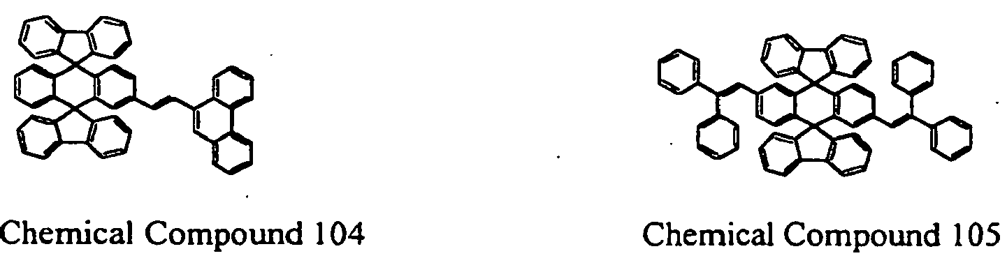


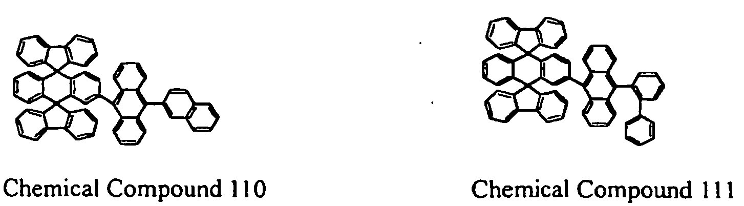


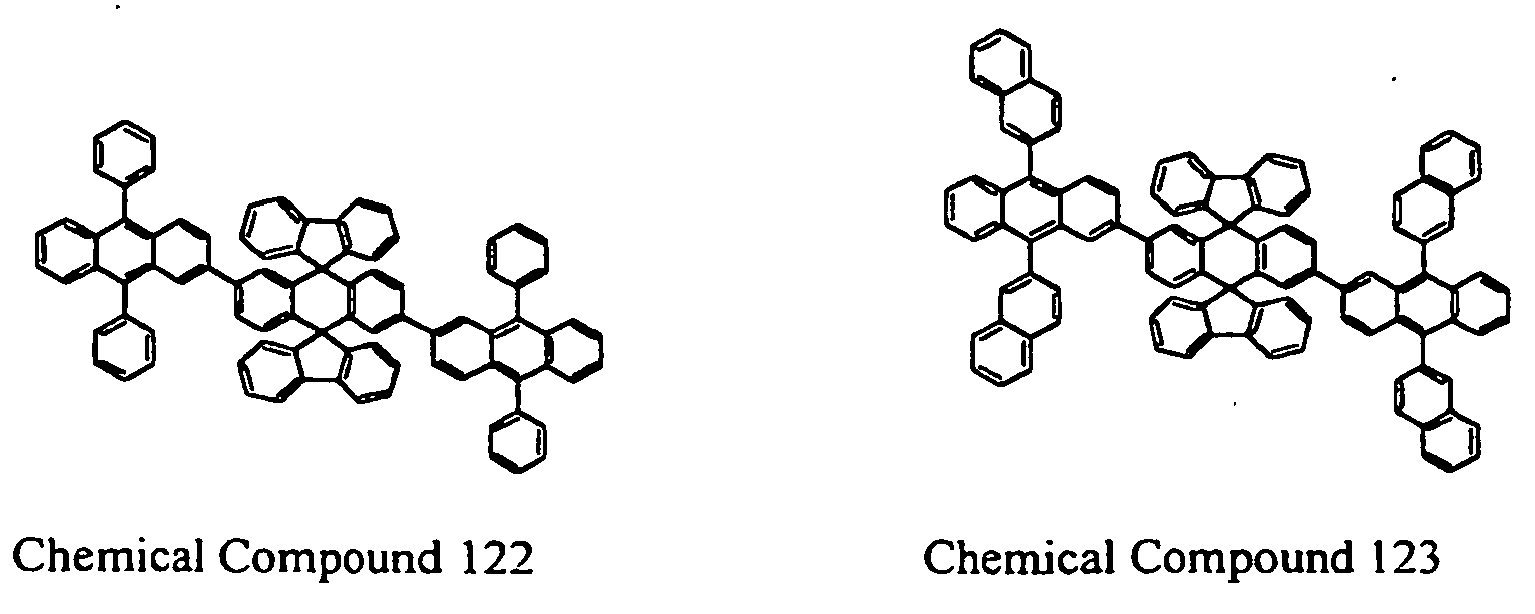


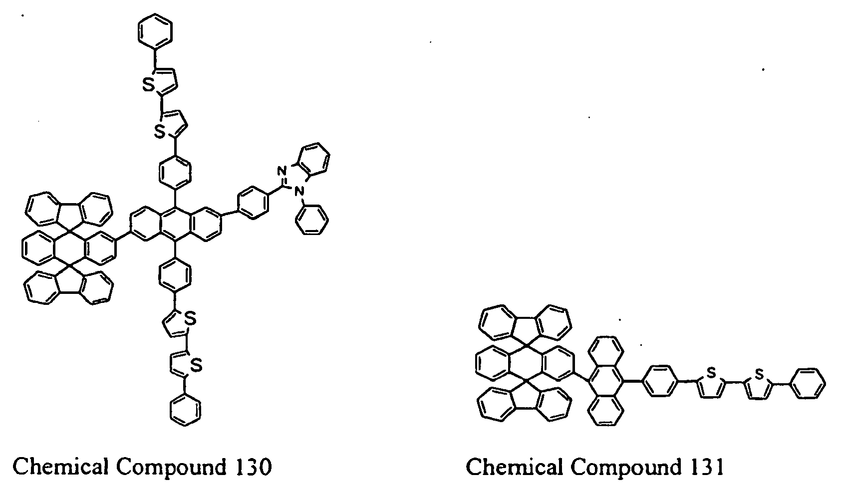
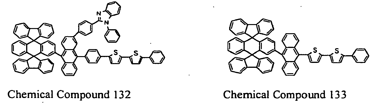


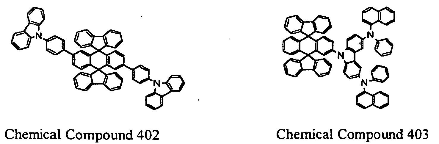
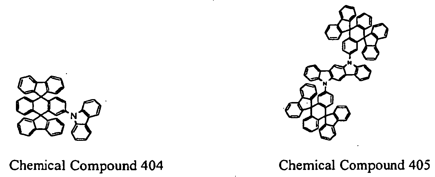
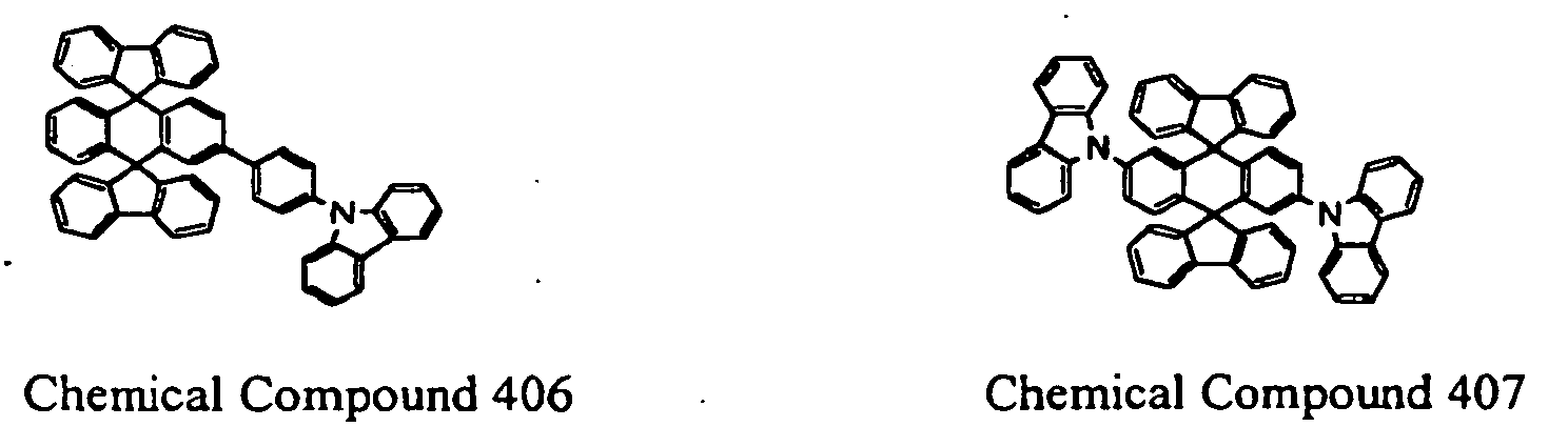


- Double-spiro organic compounds satisfying
General Formula 1 have light-emitting, hole-injecting, hole-transporting, electron injection, electron-transporting properties and characteristics, facilitating their use in the organic EL devices. Also, many of these compounds have more than one property so that they can be used to form a multifunctional layer in organic EL devices. - Many double-spiro compounds, particularly those satisfying General Formula (I), have the property of emitting visible light when appropriate energy is applied. These double-spiro compounds have their band gaps corresponding to the visible light emission. Advantageously, the band gaps of the present double-spiro compounds range from about 1.8 eV to about 3.5 eV. The double-spiro light emitting compounds generate blue, green or red light although not limited thereto. The double-spiro light emitting compounds according to the invention include, for example, Chemical Compounds 100-137, 200-222, and 400-413. The double-spiro light emitting compounds can be used to form a light-emitting layer of organic EL devices alone or in combination with other light-emitting materials, as will be discussed later. Advantageously, these light-emitting double-spiro compounds can be used to host other EL compounds having higher quantum efficiency than their own. Also, these light-emitting compounds can be used as a light-emitting dopant in a light-emitting layer with another host material or in other layers of organic EL devices.
- The double-spiro compounds of the instant invention have good electron mobility. Such compounds are candidates for use in electron transportation because good mobility of electrons in those compounds will reduce the driving voltage of the organic EL devices using the compounds. In other words, free electrons in the compounds having high electron mobility are prone to move at a low electric potential difference. Advantageously, the compounds having electron mobility of about 1x10⁻⁷ cm2/Vs or greater can be used for electron transportation. A general discussion on carrier mobility can be found in Electron Mobility in Tris(8-hydroxy-quinoline)aluminum Thin Films Determined via Transient Electroluminescence From Single- and Multiple-Layer Organic Light-Emitting Diodes, J. Appl. Phys., Vol 89, 3712 (2001); Transient Electroluminescence Measurements on Organic Heterolayer Light Emitting Diodes, Synthetic Metals 111-112, 91 (2000); and Organic Electroluminescence of Silole-Incorporated Polysilane, Journal of Luminescence 87-89, 1174 (2000).
- Also, among the compounds with good electron mobility is a group having their lowest unoccupied molecular orbital (LUMO) level relatively close to the work function of cathode materials. This group of compounds is especially suited for electron injection. This is also relevant to the driving voltage of the device because the compounds for electron injection reduce the electric potential barrier in the electron injection. Advantageously, the LUMO level of the instant compounds used for electron injection ranges from about -2.5 eV to about -4.0 eV. For example, Chemical Compounds 200-222 can be used for electron injection or transportation, or both. The double-spiro compounds with the properties of electron injection and/or transportation can be used to form an electron-injecting layer, an electron-transporting layer, or a layer having both electron injection and transportation functions in organic EL devices.
- Various double-spiro compounds of the present invention have good hole mobility. Such compounds are candidates for use in hole transportation because the good mobility of holes in those compounds will reduce the driving voltage of an organic EL device using the compounds. Holes in the compounds having high hole mobility are prone to move at a low electric potential difference. Advantageously, double-spiro compounds having hole mobility of about 1x10⁻⁷ cm2/Vs or greater can be used for hole transportation. Also, among the compounds with good electron mobility is a group having their highest occupied molecular orbital (HOMO) level relatively close to the work function of anode materials. This group of compounds is especially suited for hole injection. This is relevant to the driving voltage as well because the compounds for hole injection primarily reduce the electric potential barrier in the hole injection. Advantageously, the HOMO level of the instant compounds used for hole injection ranges from about -4.0 eV to about -6.0 eV. For example, Chemical Compounds 300-308 and 400-413 can be used for hole injection or transportation, or both. The double-spiro compounds with the properties of hole injection and/or transportation can be used to form an hole-injecting layer, an hole-transporting layer, or a layer having both hole injection and transportation functions in organic EL devices.
- Table 1 lists melting points and color of light emission of some exemplary double-spiro compounds of General Formula I.
Table 1 Chemical Compound Nos. Melting Point (°C) Color of Light Emission 100 >500 Blue 102 >500 Blue 103 430 Blue 107 365.2 Blue 109 448 Blue 110 424.8 Blue 111 475.5 Blue 113 430.3 Blue 117 462.6 Blue 118 409.8 Blue 134 395.2 Blue 135 >500 Green 200 462.9 Blue 305 353 Blue 307 315.9 Blue 308 329.2 Blue 301 370.4 Blue 303 326.0 Blue 400 358.7 Blue 401 489.5 Blue 403 413.0 Blue - As summarized in Table 1, the organic compounds of General Formula I have melting points sufficient to use in organic EL devices. The high melting point can be attributed, among other things, to the double-spiro structure with the fused six aromatic rings. Advantageously, these organic compounds have a melting point above about 300°C and glass transition temperature above about 120°C. Preferably, the melting point is above about 400°C. Given the high melting point and high glass transition temperature, morphology changes or crystallization in the thin films of these organic compounds will be less likely. Therefore, the production yield and product stability of the organic EL devices will be substantially enhanced.
- The double-spiro organic compounds of
General Formula 1 show good sublimability while at the same time the melting points thereof are sufficiently high. The sublimability of these compounds can be attributed to the structural rigidity as discussed above. On one hand, each planar moiety in the compounds holds the two dimensional rigidity with its two fused phenyl rings; on the other hand, the whole double-spiro structure has the three dimensional rigidity by balancing the spatial location of the planar moieties. The aromatic phenyl units in the compounds can also add the sublimability as well. - Further, the steric hindrance effect of the substantially perpendicular configuration of each planar moiety makes the crystallinity of the compounds substantially lower than other compounds having the same or a similar number of conjugated double bond rings. If the steric hindrance effect of a compound is high, the melting point of the compound is generally low. In the compounds of
General Formula 1, however, even if the steric hindrance effect exists, the high molecular weight keeps the melting point of the compounds sufficiently high, which prevents crystallization at a relatively low temperature. - Also, the double-spiro compounds of
General Formula 1 have relatively low crystallinity while having high aromaticity owing to the existence of six fused phenyl rings. Generally, compounds having high aromaticity are of high crystallinity and easy to crystallize. But, in the compounds of General Formula I, the conjugation of double bonds in each of the six phenyl rings does not overlap with other phenyl rings in the double-spiro structure. More particularly, the conjugations in the two phenyl groups fused with the pentagonal or hexagonal ring in each planar moiety do not overlap with each other in that planar moiety. Further, the conjugation in either of the phenyl groups of each planar moiety does not overlap with conjugation in another planer moiety of the double-spiro structure. This means that even if each planar moiety is substituted with groups forming extended conjugation with its phenyl groups, the pi-orbital overlap in the conjugation would not extend over another planar moiety and accordingly the whole molecule either. The lack of overlap of conjugation explains the relatively low crystallinity of these compounds. - Double-spiro compounds of
General Formula 1 can be synthesized in various ways. For example, certain basic double-spiro compounds are first synthesized, and then they are modified to produce more complicated double-spiro compounds. For instance, the basic double-spiro compounds have one or more reactive atoms and/or functional groups as substituents in a double-spiro skeleton. Preferably, the reactive atoms and/or functional groups are halogen atoms and any acidic leaving groups. More preferably, they are selected from the group of chlorine, bromine, iodine, p-toluenesulfonic acid, and trifluoroacetic acid. Some exemplary basic double-spiro molecules are listed below as Chemical Compounds 1-11. In these compounds, "Br" may be substituted with any other reactive atoms or functional groups.

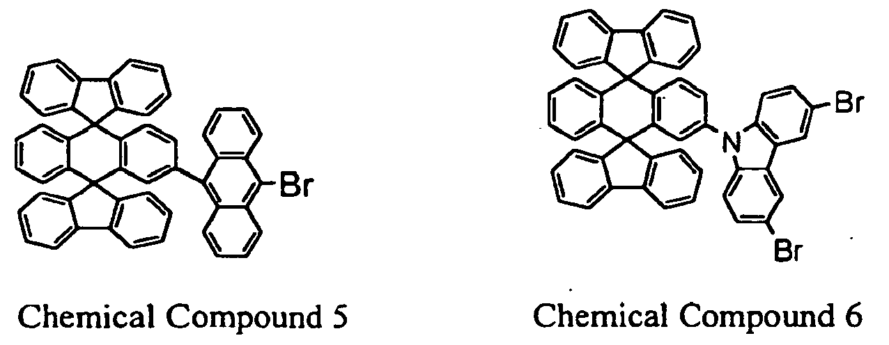
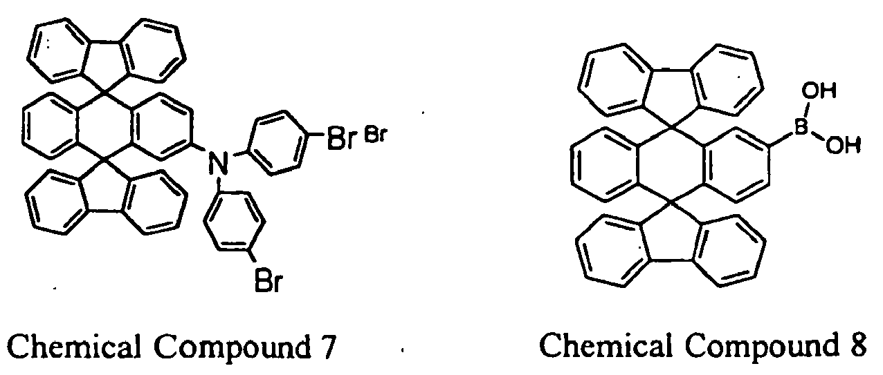


- The basic double-spiro compounds are prepared in multi-step chemical reactions. For example, certain precursor molecules are synthesized and further processed to produce basic double-spiro compounds. For example, the precursor molecules include 2-bromo-9,10-bis(2-biphenyl-hydroxy)-anthracene and 2,6-dibromo-9,10-bis(2-biphenyl-dihydroxy)-anthracene. The synthesis of 2-bromo-9,10-bis(2-biphenyl-hydroxy)-anthracene is disclosed in A Novel Acid-Catalyzed Rearrangement of 9,10-Diaryl-9,10-dihydroanthracene-9,10-diols Affording 10,10'-Diaryl-9-anthrones, Tetrahedron (1999) 55, 1759; and A General. Synthesis of Distributed Rubicenes, Eur. J. Org. Chem, (1998) 2769.
- The basic double-spiro compounds are modified to produce desired double-spiro compounds. The modification of the basic double-spiro molecules is to introduce proper substituent groups into the double-spiro moiety of the basic molecules for favorable properties for use in organic electroluminescence. Reactions that can be used in such a modification includes, for example, Suzuki-coupling, Heck-coupling and Wittig reaction.
- In a Suzuki-coupling condition, the reactive atoms or functional groups of the basic molecules are subject to reaction with boronic acid or molecules having a boronate to produce a double-spiro compounds having a new substituent group. In Heck-coupling, the reactive atoms or functional groups are reacted with compounds containing atoms for nucleophilic substitution, such as nitrogen and sulfur, to produce double-spiro compounds having substituent groups linked by a non-carbon atom. Also, under a Heck-coupling condition, basic double-spiro molecules can be reacted with compounds containing vinyl groups to obtain double-spiro molecules substituted with olefinic groups. Alternatively, double-spiro molecules having olefinic substituent groups can be produced by reacting basic double-spiro molecules with compounds containing a carbonyl group such as an aldehyde under a Wittig reaction condition. The synthesis of various double-spiro organic compounds will be further discussed in Examples 1-33.
- The present inventors have developed organic EL devices using organic compounds having one or more double-spiro structures. As discussed above, many double-spiro organic compounds have light-emitting property and other properties favorable for use in organic EL devices, including hole injection, hole transportation, electron transportation and electron injection. Various organic EL devices can be constructed with the double-spiro organic compounds of the present invention in combination with any other compounds having characteristics and properties for use in the organic EL devices. Further, some of the double-spiro organic compounds of the present invention have more than one function in the process of organic electroluminescence. With these multi-functional organic EL compounds, further various constructions of organic EL devices can be available.
- Now constructions for organic EL devices of the present invention will be discussed with reference to the accompanying drawings.
Figures 1-6 illustrate various examples of organic EL device constructions composed of a plurality of layers. In these drawings, the same reference numbers are used to indicate like components between the embodiments. The term "layer" in these illustrations refers to a thin film deposit of one or more compounds. These exemplary constructions are not exhaustive variants of the organic EL devices in accordance of the present invention. - The constructions of the organic EL device of the present invention include a
substrate 1, ananode 3, acathode 15 and one or more layers located between theanode 3 and thecathode 15, as illustrated inFigures 1-6 although not limited thereto. Advantageously, the one or more intervening layers contain at least one of the instant double-spiro organic compound. Preferably, the double-spiro compounds contained in the one or more intervening layers satisfyGeneral Formula 1. The one or more intervening layers include a hole-injectinglayer 5, a hole-transportinglayer 7, a light-emittinglayer 9, an electron-transportinglayer 11, an electron-injectinglayer 13 and combinations of more than one of these layers. - The substrate 1 (
Figures 1-6 ) supports the laminated structure of theorganic EL device 10. The anode 3 (Figures 1-6 ) and cathode 15 (Figures 1-6 ) are electrically connected to an electric power source 17 (Figures 1-6 ) via a switch 19 (Figures 1-6 ), which is controlled by a controller (not shown). The hole-injecting layer 5 (Figures 1-3 ) facilitates the injection of holes from theanode 3 into the hole-transporting layer 7 (Figures 1-5 ). Similarly, the electron-injecting layer 13 (Figures 1 and4 ) facilitates the injection of electrons from thecathode 15 into the electron-transportinglayer 13. The hole-transportinglayer 7 accelerates the movement of holes away from theanode 3 or hole-injectinglayer 5 into, for example, the light-emitting layer 9 (Figures 1-6 ). The electron-transporting layer 11 (Figures 1, 2 ,4 and5 ) accelerates the movement of electrons away from thecathode 15 or the electron-injectinglayer 13 into, for example, the light-emitting layer 9 (Figures 1-6 ). - The transferred holes and electrons recombine and form excitons at light emitting molecules in the light-emitting
layer 9. The excitons transfer the energy of the recombination to the light-emitting molecules or to other light-emitting molecules, which release the transferred energy in the form of visible light. The one or more intervening layers, although not further indicated or discussed, may be multi-functional. A multi-functional layer has functions of, for example, hole injection and transportation; electron injection and transportation; hole transportation and light emission; electron transportation and light emission; hole injection, hole transportation and light emission; electron injection, electron transportation and light emission; and so forth. Such multi-functional layers can be made of a material having multi-functional properties with or without doping of other functional materials. In the alternative such layers are made of a mixture of more than one material having different functional properties still with or without doping of other functional materials. - As mentioned above, the
substrate 1 provides a support on which the laminated construction of the organic EL device can be build. Also, thesubstrate 1 functions as a protective layer for the construction of the organic EL device once manufactured. Thus, materials for thesubstrate 1 are selected from those which can stand the conditions of manufacturing processes and usage of the organic EL devices. In some organic EL device constructions of the present invention, the light emitted from the one ormore intervening layers substrate 1. In such constructions, thesubstrate 1 is advantageously made of a transparent material to allow the visible light emitted from the light-emittinglayer 9 to pass through. Transparent materials, which can be used for thesubstrate 1, for example, include glass, quartz and any other appropriate artificial materials such as transparent plastics. Preferably, glass is used for thesubstrate 1. In other constructions of organic EL devices of the present invention, the light can be emitted through thecathode 15 or any directions other than through thesubstrate 1. In such constructions, thesubstrate 1 is advantageously made of highly reflective material satisfying thermodynamic and mechanical requirements for depositing theanode 3 thereon. For example, semiconductor wafers, metal oxide, ceramic materials, and non-transparent plastics can be used as thesubstrate 1. A transparent substrate coated with a reflective material can also be used. - The
anode 3 is a conductive electrode electrically connected to an electric power source. Theanode 3 requires a relatively large work function, advantageously greater than 4 eV. For example, conductive materials, which can be used for theanode 3, include carbon; aluminum, vanadium, chromium, copper, zinc, silver, gold, similar metals, and alloys of the foregoing metals; zinc oxide, indium oxide, induim tin oxide (hereinafter referred to as "ITO"), indium zinc oxide and similar tin oxide or tin oxide indium-based complex compounds; mixtures of oxides and metals, such as ZnO:Al, SnO2:Sb; and conductive polymers, such as poly (3-methylthiophene), poly[3,4-(ethylene-1,2-dioxy) thiophene], polypyrrole and polyaniline. Either transparent or non-transparent materials can be selected for theanode 3, depending upon the construction of the light passage in the organic EL device as discussed above in connection with the materials for thesubstrate 1. Preferably, theanode 3 is made of ITO. Although not illustrated, theanode 3 may be constructed in multiple layers of materials. The thickness of theanode 3 may vary depending on the materials used and its layered structures. However, theanode 3 is advantageously from about 10 nm to about 1000 nm, preferably from about 10 nm to about 500 nm. - The
cathode 15 requires a relatively small work function, advantageously smaller than 4 eV. For example, conductive materials, which can be used for thecathode 15, include magnesium, calcium, sodium, potassium, titanium, indium, yttrium, lithium, gadolinium, aluminum, silver, tin, lead, similar metals, and alloys of foregoing metals. Although not illustrated, thecathode 15 may be constructed in multiple layers of materials, such as LiF/Al and Li2O/Al. Preferably, thecathode 15 is made of aluminum-lithium alloy, LiF/Al or Li2O/Al. Either transparent or non-transparent materials may be used for thecathode 3, depending upon the construction of the light passage in the organic EL device as discussed above. The thickness of thecathode 15 may vary depending on the materials used and its layered structures. However, thecathode 15 is laminated advantageously from about 1 nm to about 10,000 nm, preferably from about 5 nm to about 5,000 nm. - The hole-injecting
layer 5 has the function of enabling a large number of holes to be injected from theanode 3 at a low electric field applied to the device. The hole-injectinglayer 5 advantageously is formed in the cases either where the interfacial strength betweenanode layer 3 and hole-transportinglayer 7 is not strong enough or where the work function of the anode material is significantly different from the highest occupied molecular orbital (HOMO) level of the material of its neighboringlayer anode 3 and the HOMO level of the other neighboringlayer substrate 1. In otherwise constructions, the hole-injecting material is advantageously non-transparent. - In accordance with the organic EL devices of the present invention, the hole-injecting
layer 5 can be made of one or more of the double-spiro structured compounds. Preferably, the double-spiro compounds are ofGeneral Formula 1. More preferably, the hole-injectinglayer 5 includes one or more of the Chemical Compounds 300-308 and 400-413, most preferably, Chemical Compounds 300-308. In accordance with the organic EL devices of the present invention, one or more non-double-spiro hole-injecting materials may be added. Also, the hole-injectinglayer 5 can be formed with one or more non-double-spiro hole-injecting materials as long as at least one double-spiro compound is used in the organic EL device. The non-double-spiro hole-injecting materials include, for example, metal porphyrine (U.S. Patent Nos. 4,720,432 and4,356,429 ); oligothiophene (U.S. Patent No. 5,540,999 ); arylamines and derivatives thereof (U.S. Patent Nos. 5,256,945 ,5,609,970 , and6,074,734 , andJapanese Unexamined Patent Publications 1999-219788 1996-269445 U.S. Patent No. 5,998,803 ); and anthraquinone (Japanese Unexamined Patent Publication 2000-058267 - The hole-transporting
layer 7 has the function to smoothly transfer the holes from the hole-injectinglayer 5 or from anode 3 (in the absence of the hole-injecting layer 5) toward the light-emittinglayer 9 or toward an area where light-emitting materials are doped. Materials good for use in the hole-transportinglayer 7 are those having high hole mobility therein. This hole-transportinglayer 7 also has the function of blocking electrons from its neighboringlayer cathode 15. Further, the hole-transportinglayer 7 functions for both the hole injection and hole transportation in the constructions which do not have a separate hole-injecting layer. - In accordance with the organic EL devices of the present invention, the hole-transporting
layer 7 can be made of one or more of the double-spiro structured compounds. The double-spiro compounds are preferably ofGeneral Formula 1. More preferably, the hole-transportinglayer 7 includes one or more of the Chemical Compounds 300-308 and 400-413. In accordance with the organic EL devices of the present invention, one or more non-double-spiro hole-transporting materials may be added. Also, the hole-transportinglayer 7 can be formed with one or more non-double-spiro hole-transporting materials as long as at least one double-spiro compound is used in the organic EL device. The non-double-spiro hole-transporting materials include, for example, arylamine derivatives, conjugated poylmers, block co-polymers with conjugated and nonconjugated repeating units, and the like. Advantageously, derivatives of the arylamine, 4,4'-bis[N-(1-naphthyl)-N-phenylamino]biphenyl (NPB) is used for the hole-transportinglayer 7. - The electron-transporting
layer 11 contains an electron transfer material to transfer the electron injected from theelectron injecting layer 13 or from the cathode 15 (in the absence of the electron-injecting layer 13) to the light-emittinglayer 9 or to an area where a light-emitting material is doped. Compounds having high electron mobility is used as an electron-transporting material. The electron-transportinglayer 11 may also have the function of blocking holes to move thereinto. In the construction without a separate electron-injecting layer, the electron-transporting material is selected from those which can enable a large number of electron to be injected from thecathode 15 at a low electric field applied across the device. - In accordance with the organic EL devices of the present invention, the electron-transporting
layer 11 can be made of one or more of the double-spiro structured compounds. Preferably, the double-spiro compounds are ofGeneral Formula 1. More preferably, the electron-transportinglayer 11 includes one or more of the Chemical Compounds 200-222. In accordance with the organic EL devices of the present invention, one or more non-double-spiro electron-transporting materials may be added. Also, according to the organic EL devices of the present invention, the electron-transportinglayer 11 can be formed with one or more non-double-spiro electron-transporting materials as long as at least one double-spiro compound is used in the organic EL device. The non-double-spiro electron-transporting materials include, for example, aluminum complexes of 8-hydroxyquinoline; organometallic complex compounds including Alq3 (U.S. Patent No. 5,061,569 andU.S. Patent Application No. 09/540837 ); organic radical compounds (U.S. Patent No. 5,811,833 ); hydroxyflavon-metal complexes (U.S. Patent Nos. 5,817,431 and5,516,577 ,Japanese Unexamined Patent Publications 2001-076879 2001-123157 1998-017860 - The electron-injecting
layer 13 is generally to faciliate injection of a large number of electrons from thecathode 15 at a low electric field applied across the device. The electron-injectinglayer 13 is provided when the work function of thecathode 15 significantly differs from the lowest unoccupied molecular orbital (LUMO) level of the other neighboringlayer layer 13 may be introduced to prevent excitons generated in the neighboringlayer cathode layer 15. In the alternative or in addition, the electron-injectinglayer 13 may be provided to avoid damaging theneighboring layer cathode layer 15. The LUMO level of the electron-injecting material is advantageously located between the work function of the cathode material and the LUMO level of the other neighboringlayer layer 13 is required to have strong interface with thecathode layer 15. - In accordance with the organic EL devices of the present invention, the electron-injecting
layer 13 can be made of one or more of the double-spiro structured compounds. Preferably, the double-spiro compounds are ofGeneral Formula 1. More preferably, the electron-injectinglayer 13 includes one or more of the Chemical Compounds 200-222. In accordance with the organic EL devices of the present invention, one or more non-double-spiro electron-injecting materials may be added. Also, according to the organic EL devices of the present invention, the electron-injectinglayer 13 can be formed with one or more non-double-spiro electron-injecting materials as long as at least one double-spiro compound is used in the organic EL device. The non-double-spiro electron-injecting materials include, for example, aluminum complexes of 8-hydroxyquinoline, organometallic complex compounds including Alq3, organic radical compounds (U.S. Patent No. 5,811,833 ); 3- or 5-hydroxyflavone-metal complexes (Organic Light-emitting Diodes using 3- or 5-hydroxyflavone-metal Complexes, Appl. Phys. Lett. 71 (23), 3338 (1997)); the electron-injecting compounds disclosed inJapanese Unexamined Patent Publications 2001-076879 2001-123157 1998-017860 - The light-emitting
layer 9 is a layer particularly dedicated to the emission of visible light by the process of recombination of electrons and holes therein although it may have other functions as well. Advantageously, the light-emittinglayer 9 of the organic EL devices is composed of one light-emitting material alone or a mixture of two or more light-emitting materials without doping. In an alternative construction, the light-emittinglayer 9 is composed of one or more light-emitting host materials and a small amount of one or more dopants, as will be discussed below. - In accordance with the organic EL devices of the present invention, the light-emitting
layer 9 can include one or more of the instant double-spiro structured compounds. Preferably, the double-spiro compounds are ofGeneral Formula 1 as a light-emitting material. More preferably, the light-emittinglayer 9 includes one or more of the Chemical Compounds 100-137, 200-222, and 400-413. In accordance with the organic EL devices of the present invention, these double-spiro compounds can be used as a host or as a dopant. In either case, one or more non-double-spiro light-emitting materials may be added as either another host material or another dopant. Advantageously, the double-spiro compounds are used as a host material, with or without another host material, for hosting one or more fluorescent or phosphorescent dopants. Also, according to the organic EL devices of the present invention, the light-emittinglayer 9 may include one or more non-double-spiro light-emitting materials as long as at least one double-spiro compound is used in the organic EL device. The non-double-spiro light-emitting materials include, for example, 8-hydroxyquinoline metal complexes including Alq3; carbazole compounds and derivatives thereof; dimerized styryl compounds (U.S Patent No.5,366,811 ); BAlq (U.S. Patent No 5,150,006 ); 10-hydroxybenzo [h] quinoline-metal complexes (U.S. Patent No. 5,529,853 ); 2-(2'-hydroxy-5'methylphenyl) benzotriazole metal complexes (U.S. Patent No. 5,486,406 ); benzoxazole, benzthiazole, benzimidazole and derivatives thereof (U.S. Patent No. 5,645,948 ); poly(p-phenylene vinylene) and derivatives thereof (Conjugated Polymers as Solid-State Laser Materials, Synthetic Metals 91, 35 (1997); and Low Voltage Operation of Large Area Polymer LEDs, Synthetic Metals 91, 109 (1997)); spiro compounds (U.S. Patent No. 5,840,217 ); polyfluorene, or rubrene. - According to the organic EL devices of the present invention, the light-emitting
layer 9 may be constructed with or without a dopant. Dopants are introduced to improve the light-emission efficiency, to tune the color of the emission, and/or to simply emit light from a layer having a non-fluorescent host. Dopants can be added to the light-emittinglayer 9 and one or more of theother layers layer 9 may be absent. In such constructions, one or more light-emitting dopants are necessarily put in one or more of thelayers - Generally, dopants are selected from fluorescent or phosphorescent materials having higher quantum efficiency than the host material. Preferably, the dopants have a quantum yield close to "1" in a dilute system. This means that most of the energy received from excitons contributes to the light emission rather than releasing it in other forms such as generating heat. Also, dopants are selected such that they match energetically with the host material. In other words, excitons are known to have a tendency to transfer their energy to a material having a smaller band gap among materials near the recombination location; thus, dopants are advantageously selected from the light-emitting materials having a band gap slightly smaller than that of the host materials. Depending upon the matching of the dopants and host materials, recombination may occur in the host molecules, and the energy of the generated excitons is transferred to the dopants. In this case, visible light is emitted from the dopant molecules. Also, the energy of the excitons may be transferred to another dopant, where the light is emitted. In the alternative, the recombination and light emission may occur in one light-emitting material.
- Advantageously, the double-spiro light-emitting compounds can be used as a dopant in various layers. Preferably, these dopants have the double-spiro structure of
General Formula 1. For example, Chemical Compounds 100-137, 200-222 and 400-413 can be used as a dopant light-emitting material. One or more double-spiro dopants can be used with or without other dopants. Whether or not a separate light-emitting layer is provided, quantum efficiency and lifetime of the organic EL device can be enhanced by selecting an appropriate host materials, one or more matching dopants and their concentrations. - Other light-emitting (phosphorescent or fluorescent) materials for doping in the organic EL devices of the present invention include, for example, perylene, rubrene, coumarine, quinacridone, nile red, DCM, and the following organometallic complexes.

- Some of the exemplified and additional materials for use as dopants, either fluorescent or phosphorescent, are disclosed in Organic Light-Emitting Devices With Saturated Red Emission Using 6,13-Diphenylpentacene, Appl. Phys. Lett. 78, 2378 (2001); Photoluminescence and Electroluminescence Properties of Dye-Doped Polymer System, Synthetic Metals 91, 335 (1997); Fabrication of Highly Efficient Organic Electroluminescent Devices, Appl. Phys. Lett. 73, 2721 (1998); Organic Electroluminescent Devices Doped With Condensed Polycyclic Aromatic Compounds, Synthetic Metals 91, 27 (1997); Bright Blue Electroluminescent Devices Utilizing Poly (N-Vinylcarbazole) Doped With Fluorescent Dye, Synthetic Metals 91, 331 (1997); Doped Organic Electroluminescent Devices With Improved Stability, Appl. Phys. Lett. 70, 1665 (1997); Stability Characteristics Of Quinacridone and Coumarine Molecules as Guest Dopnats in The Organic Leds, Synthetic Metals 91, 15 (1997); Strongly Modified Emission From Organic Electroluminescent Device With a Microcavity, Synthetic Metals 91, 49 (1997); Organic Light-Emitting Diodes Using a Gallium Complex, Appl. Phys. Lett. 72, 1939 (1998); Orange and Red Orgnanic Light-Emitting Devices Using Aluminum Tris (5-Hydroxyquinoxaline), Synthetic Metals 91, 217 (1997); Synthesis and Characterization of Phosphorescent Cyclometalated Iridium Complexes, Inorg. Chem. 40, 1704 (2001); Highly Phosphorescent Bis-Cyclometalated Iridium Complexes, J. Am. Chem. Soc. 123, 4304, (2001); High Quantum Efficiency in Organic Light-Emitting Devices with Iridium-Complex as Triplet Emissive Center, Jpn. J. Appl. Phys. 38, L1502 (1999); Optimization of Emitting Efficiency in Organic LED Cells Using Ir Complex, Synthetic Metals 122, 203 (2001); Operating lifetime of phosphorescent organic light emitting devices, Appl. Phys. Lett. 76, 2493 (2000); High-Efficiency Red Electrophosphorescence Devices, Appl. Phys. Lett. 78, 1622 (2001); Very High-Efficiency Green Organic Light-Emitting Devices Based on Electrophosphorescence, Appl. Phys. Lett. 75, 4 (1999); Highly-Efficient Organic Electrophosphorescent Devices With Tris(2-Phenylpyridine)Iridium Doped Into Electron-Transporting Materials, Appl. Phys. Lett. 77, 904 (2000); and Improved Energy Transfer In Electrophosphorescent Devices, Appl. Phys. Lett. 74, 442 (1999).
- Other various aspects and features of the double-spiro compounds and organic EL devices in accordance with the present invention will be further discussed in terms of the following examples, which are intended to illustrate the present invention but not limit the scope.
- To a solution of 2-bromobiphenyl (9.00 ml, 52.0 mmol) in THF (100 ml) was added dropwise t-BuLi (40 ml of a 1.7 M solution in pentane) at -78 °C under nitrogen. After the mixture had been stirred for 40 min, 2-bromoanthraquinone (5.00 g, 17.0 mmol) was added at -78 °C. The cooling bath was removed and the mixture was stirred for 3 hours at room temperature. The reaction mixture was poured into diethyl ether (150 ml) and 2 N HCl (150 ml), and stirred for 40 min at room temperature. The precipitate was filtered off with suction, washed with water and ethyl ether, and then dried to obtain 2-bromo-9,10-bis(2-biphenyl-hydroxy)-anthracene (9.50 g, 92%).

- 2-bromo-9,10-bis(2-biphenyl-dihydroxy)-anthracene 9.50 g (16.0 mmol) of 2-bromo-9,10-bis(2-biphenyl-hydroxy)-anthracene synthesized as above was suspended in acetic acid (150 ml), and conc. H2SO4(20 drops) was added thereto. After the reaction mixture had been stirred at reflux for about 3 hours, it was cooled to room temperature. The precipitate was filtered off with suction, washed with acetic acid, water, and ethanol. Purification by sublimation afforded Chemical Compound 2 (8.0 g, 89%) as white solid: mp 419.7 °C; 1H NMR (500 MHz, DMSO-d6) δ 8.12 (dd, J= 7.4, 7.3 Hz, 4H), 7.53-7.47 (m, 4H), 7.39-7.34(m, 4H), 7.25 (t, J = 8.0 Hz, 4H), 7.06 (dd, J = 2.3, 8.7 Hz, 1H), 6.86-6.81 (m, 2H), 6.29 (d, J= 2.3 Hz; 1H), 6.26-6.21 m, 2H), 6.20 (d, J = 8.7 Hz, 1H); MS (M+) calculated for C38H23Br 558, found 558; analysis calculated for C38H233Br: C, 81.58; H, 4.14; Br, 14.28. Found: C, 82.00; H, 4.14; Br, 13.86.
- To a solution of 2-bromobiphenyl (8.83 ml, 51.2 mmol) in THF (200 ml) was added dropwise t-BuLi (60 ml of a 1.7 M solution in pentane) at -78 °C under nitrogen. After the mixture had been stirred for 40 min, 2,6-dibromoanthraquinone (7.50 g, 20.5 mmol) was added at -78 °C. The cooling bath was removed and the mixture was stirred for 15 hours at room temperature. The reaction mixture was poured into diethyl ether (200 ml) and 2 N HCl (200 ml), and stirred for 40 min at room temperature. The precipitate was filtered off with suction, washed with water and ethyl ether. After drying, 2,6-dibromo-9,10-bis(2-biphenyl-dihydroxy)-anthracene (11.8 g, 85%) was obtained.

- 2,6-dibromo-9,10-bis(2-biphenyl-dihydroxy)-anthracene 10.5 g (15.57 mmol) of 2,6-dibromo-9,10-bis(2-biphenyl-hydroxy)-anthracene synthesized as above was suspended in acetic acid (150 ml), and conc. H2SO4(20 drops) was added thereto. After the reaction mixture had been stirred while refluxing for about 15 hours, it was cooled to room temperature. The precipitate was filtered off with suction, washed with acetic acid, water, and ethanol. Purification by sublimation afforded Chemical Compound 2 (9.0 g, 90%) as white solid: mp 478.1 °C; 1H NMR (300 MHz, CDCl3) δ 7.92 (d, J= 7.6 Hz, 4H), 7.46 (t, J = 8.0 Hz, 4H), 7.33 (t, J = 7.4 Hz, 4H), 7.21 (d, J = 7.6 Hz, 4H), 6.88 (dd, J = 2.1, 8.6 Hz, 2H), 6.47 (d, J = 2.1 Hz, 2H), 6.22 (d, J= 8.6 Hz, 2H); MS (M+) calculated for C38H22Br2 636, found 636; analysis calculated for C38H22Br2: C, 71.50; H, 3.47; Br, 25.03. Found: C, 71.90; H, 3.40; Br, 25.7.
- To a solution of 2-methylanthraquinone (16.0 g, 72.0 mmol) in a mixture of acetic acid (400 ml) and acetic anhydride (400 ml) was added concentrated sulfuric acid (16 ml) at 5 °C. Chromium trioxide (18.0 g, 0.18 mmol) was added over a period of 1 hour at 5 °C. The reaction mixture was then stirred at 5 °C for 4 hours, poured into ice water, and extracted with chloroform. The organic extract was dried over MgSO4 and concentrated under vacuum to give anthraquinone-2-aldehyde diacetate (16.0 g, 65%.) To a solution of the anthraquinone-2-aldehyde diacetate (16.0 g, 47.3 mmol) in acetic acid (400 ml) was added dropwise 35% aqueous hydrochloric acid (170 ml) at room termperature. The reaction mixture had been stirred while refluxing for 15 min, cooled to room temperature, filtered off with suction, and washed with water. After drying, anthraquinone-2-aldehyde (10.0 g, 89%) was obtained.
- A mixture of anthraquinone-2-aldehyde (12.0 g), 1,3-propanediol (10 ml), and p-toluenesulfonic acid (20 mg) in toluene (300 ml) was heated under reflux with a removal of water formed from the condensation of anthraquinone aldehyde and 1,3-propane diol for 4 hours. The mixture was then cooled to room temperature, filtered off with suction, washed with water and diethyl ether, and dried under vacuum to afford anthraquinone-2-propaneacetal (12.5 g, 84%).
- To a solution of 2-bromobiphenyl (9.3 ml, 54.0 mmol) in THF (80 ml) was added dropwise t-BuLi (45 ml of a 1.7 M solution in pentane) at -78 °C under nitrogen. After the mixture had been stirred for 1 hour, anthraquinone-2-propaneacetal (6.60 g, 22.4 mmol) was added at -78 °C. The cooling bath was removed and the mixture was stirred for 1h at room temperature. The mixture was poured into 1 N HCl and diethyl ether, and then stirred for 1 hour, precipitate formed was filtered off with suction, washed with diethyl ether, and dried under vacuum to give anthraquinol-2-propaneacetal (13.0 g, 93%).
- To a solution of anthraquinol-2-propaneacetal (13.0 g, 21.5 mmol) in acetic acid (300 ml) was added concentrated sulfuric acid (5 drops). The reaction mixture had been stirred while refluxing for 3 hours, it was cooled to room temperature. The precipitate was filtered off with suction, washed with water, ethanol, and diethyl ether, and dried under vacuum to afford Chemical Compound 3 (10.0 g, 91%) as white solid: mp 428.5 °C; 1H NMR (300 MHz, CDCl3) δ 9.53 (s, 1H), 8.15-8.13 (m, 4H), 7.52-7.23 (m, 13H), 6.85-6.82 (m, 2H), 6.79 (s, 1H), 6.45 (d, J= 8.2 Hz, 1H), 6.26-6.22 (m, 2H).
- For the coupling of the halogen containing precursor molecules to prepare appropriately substituted double-spiro compounds, the halogen of
Chemical Compound 1 was converted into a boronic acid group as in Chemical Compound 8. - To a solution of Chemical Compound 1 (10.0 g, 17.9 mmol), in dry THF (150 ml) was added dropwise t-BuLi (31.5 ml of a 1.7 M solution in pentane) at - 78 °C under nitrogen. After the mixture had been stirred for 1 hour, trimethylborate (8.00 ml, 71.5 mmol) was added dropwise at -78 °C. The cooling bath was removed and the mixture was stirred for 3 hours at room temperature. The mixture was quenched with 2 N HCl (100 ml) and stirred for 1 hour at room temperature. The precipitate was filtered with suction and washed with water. The crude product was slurried in diethyl ether, stirred while refluxing , filtered off with suction, and dried under vacuum at 50 °C. After drying, double-spiro boronic acid of Chemical Compound 8 (7.60 g, 81 %) was obtained, and used for the Suzuki-coupling reaction without further purification
- To a solution of Chemical Compound 3 (1.34 g, 2.6 mmol) and 4,4'-bis(diethylphosphorylmethyl)biphenyl (0.50 g, 1.3 mmol) in DMF (80 ml) was added dropwise lithium ethoxide (2.8 ml of a 1.0 M solution in ethanol) at room temperature under nitrogen. After the reaction mixture had been stirred at room temperature for 12 hours, it was filtered off with suction, washed with ethanol and dried under vacuum. Purification by sublimation afforded Chemical Compound 100 (1.00 g, 66%) as white solid: mp > 500 °C; 1H NMR is not listed because of insolubility of Chemical Compound 100 in common solvents. MS (M+) calculated for C90H56 1136, found 1136; analysis calculated for C90H56: C, 95.04; H, 4.96. Found: C, 94.88; H, 5.12.
- To a suspension of 9,10-dibromoanthracene (60 mg 0.19 mmol), Chemical Compound 8 (0.20 g, 0.38 mmol), and potassium phosphate (0.16 g, 0.76 mmol) in DMF (10 ml) was added tetrakis(triphenylphosphine)palladium (12 mg, 0.01 mmol) under nitrogen. After the reaction mixture had been stirred at 60 °C for 18 hours, it was cooled to room temperature and ethanol (20 ml) was added. After addition, the reaction mixture was further stirred at room temperature for 30 minutes. The precipitate was filtered off with suction, washed with water, ethanol, and acetone, and dried under vacuum. Then it was dissolved in N-methyl pyrrolidine (50 ml) and filtered through a short column packed with silica gel. After removal of solvent, the crude product was purified by crystallizing from ethanol to give Chemical Compound 102 (0.16 g, 41%): mp > 500 °C; 1H NMR is not listed because of insolubility of 100 in common solvents. MS (M+) calculated for C90H54 1134, found 1134; analysis calculated for C90H54: C, 95.21; H, 4.79. Found: C, 94.90; H, 4.70.
- To a suspension of Chemical Compound 1 (0.50 g, 0.89 mmol), 1-vinylpyrene (0.25 g, 1.07 mmol), and triethylamine (1.5 ml, 10.8 mmol)) in DMF (8 ml) were added Pd(OAc)2 (11 mg, 0.05 mmol) and tri-o-tolylphosphine (70 mg, 0.23 mmol). After the reaction mixture had been stirred while refluxing for 15 hours, it was cooled to room temperature, quenched with water (40 ml), and extracted with dichloromethane (3 x 40 ml). The combined organic extracts were dried over MgSO4 and concentrated under vacuum. Purification by column chromatography (1:2 dichloromethane-hexane) and recrystillization from THF and ethanol afforded Chemical Compound 103 (0.2 g, 32%) as yellow solid: mp 430.0 °C; 1H NMR (300 MHz, CDCl3) δ 8.18-7.70 (m, 14H), 7.47-7.25 (m, 14H), 6.90-6.78 (m, 2H), 6.52-6.41 (m, 4H); MS (M+) calculated for C56H34 706, found 706; analysis calculated for C56H34: C, 95.15; H, 4.85. Found: C, 95.10; H, 4.66.
- To a solution of 1,1'-diphenylethylene (7.80 g, 43.3 mmol) in carbon tetrachloride (250 ml) in dark atmosphere was added dropwise bromine (2.45 ml) in carbon tetrachloride (5 ml) at -15 °C. The reaction mixture was stirred at room temperature for 1 hour and silica gel (SiO2, 1.0 g), which was activated at 140 °C for 15h, was added. After the mixture had been stirred while refluxing for 1 hour, it was cooled to room temperature. After removal of the solvent, the residue was dissolved with n-hexane and filtered through a short column packed with silica gel. Recrystallization from n-hexane afforded 2,2'-diphenylvinyl-1-bromide (10.6 g, 95%) as ivory crystal.
- To a solution of 2,2'-diphenylvinyl-1-magnesium bromide, which was freshly prepared from 2,2'-diphenyl-1-bromide (2.00 g, 7.72 mmol) in THF (30 ml) and magnesium (0.23 g, 9.24 mmol) with iodomethane (3 drops) as an initiator, was added dropwise trimethylborate (2.63 ml, 23.16 mmol) in THF (6 ml) at -78 °C under nitrogen. After the mixture had been stirred at room temperature for 3 hours, it was poured into a mixture of 2 N HCl (40 ml) and diethyl ether (200 ml). The organic layer was separated, dried over MgSO4, and concentrated under vacuum. Chemical Compound 2 (0.36 g, 0.75 mmol), 2,2'-diphenylvinyl-1-boronic acid, and tetrakis(triphenylphosphine)palladium (86 mg, 0.075 mmol) were slurried in a mixture of toluene (20 ml) and aqueous potassium carbonate solution (10 ml, 2 M). With vigorous stirring, the mixture was boiled under reflux for 10 hours. After cooling to room temperature, the organic layer was separated, washed with water, dried over MgSO4, and concentrated under vacuum. Recrystallization from chloroform and ethanol afforded Chemical Compound 105 (0.42 g, 67%) as white solid: mp 387.7 °C; 1H NMR (300 MHz, CDCl3) δ 7.44 (d, J = 7.4 Hz, 4H), 7.37 (t, J = 7.4 Hz, 4H), 7.23 (t, J = 8.8 Hz, 4H), 7.14-6.98 (m, 20H), 6.81 (d, J = 8.0 Hz, 4H), 6.43 (s, 2H), 6.34 (d, J = 8.4 Hz, 2H), 6.10 (s, 2H), 6.01 (d, J= 8.4 Hz, 2H); MS (M+) calculated for C66H44 836, found 836; analysis calculated for C66H44: C, 94.70; H, 5.30. Found: C, 94.30; H, 5.40.
- To a solution of Chemical Compound 1 (1.20 g, 2.14 mmol), 4-(2,2-diphenylvinyl)-phenylboronic acid (0.64 g, 2.14 mmol), and sodium carbonate (0.68 g, 6.42 mmol) in a mixture of toluene (30 ml), ethanol (6 ml), and water (15 ml) was added tetrakis(triphenylphosphine)palladium (50 mg, 0.04 mmol). The reaction mixture was stirred while refluxing for 12 hours. Then it was cooled to room temperature and water (50 ml) was added. The organic layer was separated and the aqueous layer was extracted with dichloromethane (3 x 50 ml). The combined organic extracts were dried over MgSO4 and concentrated under vacuum. Recrystllization from chloroform and ethanol afforded Chemical Compound 107 (0.98 g, 62%) as colorless solid: mp 365.2 °C; 1H NMR (500 MHz, CDCl3) δ 7.92 (dd, J = 4.6, 7.4 Hz, 4H), 7.45-7.39 (m, 4H), 7.32-7.22 (m, 17H), 7.15-7.13 (m, 2H), 6.96 (dd, J = 2.0, 8.5 Hz, 1H), 6.89 (s, 3H), 6.84 (s, 1H), 6.79-6.75 (m, 2H), 6.55 (d, J = 2.0 Hz, 1H), 6.43-6.36 (m, 3H); MS (M+) calculated for C58H38 734, found 734; analysis calculated for C58H38: C, 94.79; H, 5.21. Found: C, 94.98; H, 5.05.
- To a suspension of 9-bromo-10-phenylanthracene (0.3 g, 1.00 mmol), Chemical Compound 8 (0.52 g, 1.00 mmol), and potassium phosphate (0.42 g, 2.00 mmol)) in DMF (10 ml) was added tetrakis(triphenylphosphine)palladium (35 mg, 0.03 mmol) under nitrogen. After the reaction mixture had been stirred at 60 °C for 12 hours, it was cooled to room temperature. Ethanol (20 ml) was added to the mixture, and then the mixture was stirred for 30 minutes at room temperature. The precipitate was filtered off with suction, washed with water, ethanol, and acetone, and dried under vacuum. Then it was dissolved in chloroform (150 ml) and filtered through a short column packed with silica gel. After removal of solvent, the crude product was purified by crystallizing from ethanol to give Chemical Compound 109 (0.26 g, 35%): mp 448 °C; 1H NMR (400 MHz, N-methylpyrrolidine-d9) δ 8.26 (d, J = 7 Hz, 2H), 8.00 (dd, J = 3.0, 7.0 Hz, 2H), 7.62-7.54 (m, 9H), 7.48-7.38 (m,9H), 7.35-7.29 (m, 5H), 7.20-7.16 (m, 2H), 7.10 (dd, J = 2.0, 8.0 Hz, 1H), 6.95-6.90 (m, 2H), 6.66 (d, J = 8.0 Hz, 1H), 6.49 (d, J = 2.0 Hz, 1H), 6.42-6.39 (m, 2H); MS (M+) calculated for C58H36 732, found 732; analysis calculated for C58H36: C, 95.05; H, 4.95. Found: C, 95.07; H, 4.88.
- To a suspension of 9-bromo-10-(2-naphtyl)-anthracene (1.00 g, 2.60 mmol), Chemical Compound 8 (1.36 g, 2.60 mmol), and potassium phosphate (1.10 g, 5.20 mmol)) in DMF (60 ml) was added tetrakis(triphenylphosphine)palladium (90 mg, 0.08 mmol) under nitrogen. After the reaction mixture was stirred at 70 °C for 12 hours, it was cooled to room temperature and ethanol (60 ml) was added. After addition, the reaction mixture was stirred at room temperature for 30 minutes. The precipitate was filtered off with suction, washed with water, ethanol, and acetone, and dried under vacuum. Then, it was dissolved in chloroform (450 ml) and filtered through a short column of silica gel. After removal of solvent, the crude product was purified by crystallizing from ethanol to give of Chemical Compound 110 (1.20 g, 58%): mp 423 °C; 1H NMR (400 MHz, CDCl3) δ 8.00-7.96 (m, 4H), 7.84-7.81 (m, 2H), 7.76-7.71 (m, 2H), 7.58-7.33 (m, 19H), 7.18-7.06 (m, 4H), 6.97 (ddd, J = 2.0, 4.0, 8.0 Hz, 1H), 6.85-6.80 (m, 2H), 6.65 (d, J = 8.0 Hz, 1H), 6.57 (dd, J = 2.0, 5.0 Hz, 1H), 6.50-6.45 (m,2H); MS (M+) Calculated for C62H38 782, found 782; analysis calculated for C62H38: C, 95.11; H, 4.89. Found: C, 95.20; H, 4.80.
- To a suspension of 9-bromo-10-(2-biphenyl) anthracene (0.4 g, 1.00 mmol), Chemical Compound 8 (0.52 g, 1.00 mmol), and potassium phosphate (0.42 g, 2.00 mmol)) in DMF (10 ml) was added tetrakis(triphenylphosphine)palladium (35 mg, 0.03 mmol) under nitrogen. After the reaction mixture had been stirred at 60 °C for 12 hours, it was cooled to room temperature and ethanol (20 ml) was added. After addition, the reaction mixture was stirred at room temperature for 30 minutes. The precipitate was filtered off with suction, washed with water, ethanol, and acetone, and dried under vacuum. Then, it was dissolved in chloroform (150 ml) and filtered through a short column of silica gel. After removal of solvent, the crude product was purified by sublimation to give Chemical Compound 111 (0.26 g, 35%): mp 475.5 °C; 1H NMR (400 MHz, CDCl3) δ 7.97 (d, J = 7.0 Hz, 2H), 7.81 (d, J = 7.0 Hz, 1H), 7.74-7.70 (m, 2H), 7.56-7.20 (m, 18H), 7.14-7.10 (m, 2H), 7.00-6.70 (m, 11H), 6.58 (d, J= 8.0 Hz, 1H), 6.53-6.42 (m, 3H); MS (M+) Calculated for C64H40 808, found 808; analysis calculated for C64H40: C, 95.02; H, 4.98. Found: C, 95.14; H, 4.86.
- To a suspension of 9-bromo-10-(3,5-terphenyl)-anthracene (0.78 g, 1.50 mmol), Chemical Compound 8 (0.79 g, 1.50 mmol), and potassium phosphate (0.63 g, 3.00 mmol)) in DMF (25 ml) was added tetrakis(triphenylphosphine)palladium (52 mg, 0.05 mmol) under nitrogen. After the reaction mixture had been stirred at 70 °C for 12 hours, it was cooled to room temperature and ethanol (30 ml) was added. After the addition, the reaction mixture was stirred at room temperature for 30 minutes. The precipitate was filtered off with suction, washed with water, ethanol, and acetone, and dried under vacuum. Then, it was dissolved in chloroform (50 ml) and filtered through a short column of silica gel. After removal of the solvent, the crude product was purified by crystallizing from ethanol to give Chemical Compound 113 (0.75 g, 57%): mp 430.3 °C; 1H NMR (400 MHz, CDCl3) δ 7.99-7.96 (m, 3H), 7.75-7.66 (m, 8H), 7.59 (dt, J = 2.0, 10.0 Hz, 2H), 7.51-7.30 (m, 20H), 7.24-7.19 (m, 2H), 7.11-7.07 (m, 2H), 6.96 (dd, J = 2.0, 8.0 Hz, 1 H), 6.85-6.80 (m, 2H), 6.65 (d, J = 8.0 Hz, 1 H), 6.57 (d, J = 2.0 Hz, 1H), 6.50-6.45 (m, 2H); MS (M+) Calculated for C70H44 884, found 884; analysis calculated for C70H44: C, 94.99; H, 5.01. Found: C, 95.03; H, 4.93.
- To a suspension of Chemical Compound 2 (0.33 g, 0.51 mmol), 10-phenyl-anthracene-9-boronic acid (0.53 g, 1.79 mmol), potassium phosphate (0.43 g, 2.00 mmol), and 2,6-di-t-butyl-4-methylphenol (80 mg, 0.36 mmol) in DMF (10 ml) was added tetrakis(triphenylphosphine)palladium (24 mg, 0.02 mmol) under nitrogen. The mixture was degassed with nitrogen for 1 hour. After the reaction mixture had been stirred at 65 °C for 17 hours, it was cooled to room temperature and ethanol (50 ml) was added. After addition, the reaction mixture was stirred at room temperature for 30 minutes. The precipitate was filtered off with suction, washed with water and ethanol, and dried under vacuum. Purification by sublimation afforded Chemical Compound 114 (60 mg, 12%) as white solid: mp > 500 °C; 1H NMR is not listed because of insolubility of Chemical Compound 114 in common solvents. MS (M+) Calculated for C78H48 984, found, 984; analysis calculated for C78H48: C, 95.09; H, 4.91. Found: C, 95.15; H, 4.85.
- To a suspension of 2-bromo-9,10-diphenylanthracene (0.41 g, 1.00 mmol), Chemical Compound 8 (0.79 g, 1.50 mmol), and potassium phosphate (0.64 g, 3.00 mmol)) in DMF (15 ml) was added tetrakis(triphenylphosphine)palladium (35 mg, 0.03 mmol) under nitrogen. The mixture was degassed with nitrogen for 30 minutes. After the reaction mixture had been stirred at 90 °C for 60 hours, it was cooled to room temperature and ethanol (60 ml) was added. After addition, the reaction mixture was stirred at room temperature for 30 minutes. The precipitate was filtered off with suction, washed with water and ethanol, and dried under vacuum. Purification by sublimation afforded Chemical Compound 116 (0.32 g, 40%) as white solid: mp 399.06 °C; 1H NMR (500 MHz, CDCl3) δ 7.90 (dd, J= 7.0, 13.0 Hz, 4H), 7.62-7.37 (m, 19H), 7.31-7.22 (m, 9H), 7.05 (dd, J = 2.0, 8.0 Hz, 1H), 6.96 (dd, J = 2.0, 8.0 Hz, 1H), 6.79-6.75. (m, 2H), 6.56 (d, J = 2.0 Hz, 1H), 6.41-6.36 (m, 3H); MS (M+) Calculated for C64H40 808, found 808; analysis calculated for C64H40: C, 95.02; H, 4.98. Found: C, 95.10; H, 4.90.
- To a solution of 2-bromonaphthalene (6.49 g, 31.3 mmol) in dry THF (50 ml) was added dropwise t-BuLi (18.4 ml of a 1.7 M solution in pentane) at -78 °C under nitrogen. After the mixture had been stirred for 30 min, 2-bromoanthraquinone (3.00 g, 10.4 mmol) was added at -78 °C. The cooling bath was removed and the mixture was stirred for 2 hours at room temperature. The mixture was quenched with saturated aqueous ammonium chloride solution (50 ml) and extracted with ethyl ether (3 x 50 ml). The combined organic extracts were dried over MgSO4 and concentrated under vacuum. The crude product was slurried in petroleum ether, filtered off with suction, and washed with petroleum ether. After drying, the 2-bromo-9,10-di-naphthalene-2-yl-9,10-dihydro-anthracene-9,10-diol (5.30 g, 93%) was obtained.
- A mixture of the diol (5.43 g, 10 mmol) obtained above, potassium iodide (15 g), and sodium hypophosphite hydrate (15 g) in acetic acid (100 ml) was stirred while refluxing for 1 hour under nitrogen. After cooling the mixture to room temperature, the precipitate was filtered off with suction and washed with water and methanol. After drying, 2-bromo-9,10-(di-2-naphtyl)-anthracene (4.00 g, 79%) was obtained.
- To a solution of 2-bromo-9,10-(di-2-naphtyl)-anthracene (0.60 g, 1.18 mmol), Chemical Compound 8 (0.62 g, 1.18 mmol), and sodium carbonate (0.38 g, 3.54 mmol) in a mixture of toluene (30 ml), ethanol (6 ml), and water (10 ml), tetrakis(triphenylphosphine)palladium (27 mg, 0.02 mmol) was added. The reaction mixture was stirred while refluxing for 24 hours and quenched with conc. HCl (1 ml). Then it was cooled to room temperature and extracted with dichlomethane (3 x 30 ml). The combined organic extracts were dried over MgSO4 and concentrated under vacuum. The residue was dissolved in chloroform, filtered through a short column of silica gel, and concentrated under vacuum. Recrystallization from chloroform and ethanol afforded Chemical Compound 117 (0.70 g, 65%) as pale yellow solid: mp 462.6 °C; 1H NMR (500 MHz, DMSO-d6) δ 8.36 (d, J = 8.3 Hz, 1H), 8.18-7.97 (m, 8H), 7.88-7.74 (m, 4H), 7.64-7.51 (m, 6H), 7.48-7.40 (m, 4H), 7.37-7.02 (m, 15H), 6.82-6.77 (m, 2H), 6.30-6.15 (m, 4H); MS (M+) Calculated for C72H44 908, found 908; analysis calculated for C72H44: C, 95.12; H, 4.88. Found: C, 95.36; H, 4.64.
- To a suspension of 2-bromo-9,10-bis(2-biphenyl) (0.56 g, 1.00 mmol), Chemical formula 8 (0.79 g, 1.50 mmol), and potassium phosphate (0.64 g, 3.00 mmol)) in DMF (10 ml) was added tetrakis(triphenylphosphine)palladium (35 mg, 0.03 mmol) under nitrogen. The mixture was degassed with nitrogen for 30 min. After the reaction mixture had been stirred at 90 °C for 18 hours, it was cooled to room temperature and ethanol (50 ml) was added. After addition, the reaction mixture was stirred at room temperature for 30 minutes. The precipitate was filtered off with suction, washed with water and ethanol, and dried under vacuum. Then it was dissolved in chloroform (500 ml), filtered through a short column of silica gel, and concentrated under vacuum. Purification by sublimation afforded Chemical Compound 118 (0.63 g, 66%) as white solid: mp 409.8 °C; 1H NMR (500 MHz, CDCl3) δ 7.96 (d, J = 7.4 Hz, 2H), 7.91 (dd, J = 4.6, 7.4 Hz, 2H), 7.59-7.12 (m, 26H), 6.97 (ddd, J= 2.3, 8.7, 14.2 Hz, 2H), 6.87-6.73 (m, 8H), 6.68-6.63 (m, 4H), 6.60 (d, J = 1.9 Hz, 1H), 6.41 (d, J = 8.7 Hz, 1H), 6.40-6.36 (m, 2H); MS (M+) Calculated for C76H48 960, found 960; analysis calculated for C76H48: C, 94.79; H, 5.03. Found: C, 95.10; H, 4.89.
- To a solution of 1,3,5-tribromobenzene (10.0 g, 31.8 mmol), phenylboronic acid (9.68 g, 79.4 mmol), and sodium carbonate (25.3 g, 0.24 mol) in a mixture of toluene (150 ml), ethanol (30 ml), and water (75 ml), tetrakis(triphenylphosphine)palladium (1.84 g, 5 mol%) was added. The reaction mixture was stirred while refluxing for 24 hours and quenched with conc. HCl (20 ml). Then it was cooled to room temperature and extracted with ethyl ether (3 x 50 ml). The combined organic extracts were dried over MgSO4 and concentrated under vacuum. Purification by column chromatography (n-hexane) afforded 3,5-(diphenyl)bromobenzene (9.82 g, 51%)
- To a solution of 3,5-(diphenyl)bromobenzene (5.00 g, 16.2 mmol) in dry THF (50 ml) was added dropwise t-BuLi (9.53 ml of a 1.7 M solution in pentane) at -78 °C under nitrogen. After the mixture had been stirred for 30 min, 2-bromoanthraquinone (1.55 g, 5.39 mmol) was added at -78 °C. The cooling bath was removed and the mixture was stirred for 2 hours at room temperature. The mixture was quenched with saturated aqueous ammonium chloride solution (50 ml) and extracted with ethyl ether (3 x 50 ml). The combined organic extracts were dried over MgSO4 and concentrated under vacuum. The crude product was slurried in petroleum ether, filtered off with suction, and washed with petroleum ether. After drying, 2-bromo-9,10-[1,1',3',1"]terphenyl-5'-yl-9,10-dihydro-anthracene-9,10-diol (3.00 g, 74%) was obtained.
- A mixture of the diol obtained above (2.24 g, 3.0 mmol), potassium iodide (2.25 g, 13.6 mmol), and sodium hypophosphite hydrate (2.25 g, 25.6 mmol) in acetic acid (30 ml) was stirred while refluxing for 1 hour under nitrogen. After cooling to room temperature, the precipitate was filtered off with suction, and washed with water and methanol. After drying, 2-bromo-9,10-[1,1',3',1"]terphenyl-5'-yl -anthracene (1.75 g, 82%) was obtained.
- To a solution of 2-bromo-9,10-[1,1',3',1"]terphenyl-5'-yl-anthracene (0.5 g, 0.70 mmol), Chemical Compound 8 (0.55 g, 1.05 mmol), and sodium carbonate (0.22 g, 2.1 mmol) dissolved in a mixture of toluene (30 ml), ethanol (6 ml), and water (10 ml), tetrakis(triphenylphosphine)palladium (16 mg, 2 mol%) was added. The reaction mixture was stirred while refluxing for 24 hours and quenched with conc. HC1 (1 ml). Then, it was cooled to room temperature and extracted with dichlomethane (3 x 30 ml). The combined organic extracts were dried over MgSO4 and concentrated under vacuum. The residue was dissolved in chloroform, filtered through a short column of silica gel, and concentrated under vacuum. Recrystallization from chloroform and ethanol afforded Chemical Compound 119 (0.45 g, 58%) as pale yellow solid: mp 512.8 °C; 1H NMR (500 MHz, DMSO-d6) δ 8.38 (s, 1H), 8.15-7.82 (m, 11H), 7.75-7.38 (m, 20H), 7.32-7.05 (m, 16H), 6.82-6.75 (m, 3H), 6.38-6.10 (m, 5H); MS (M+) Calculated for C88H56 1112, found 1112; analysis calculated for C88H56: C, 94.93; H, 5.07. Found: C, 95.18; H, 4.82.
- To a suspension of 2-bromo-9,10-di[2-(2'-phenyl)biphenyl]-anthracene (0.40 g, 0.56 mmol), Chemical Compound 8 (0.63 g, 1.12 mmol), and potassium phosphate (0.36 g, 1.68 mmol)) in DMF (40 ml) was added tetrakis(triphenylphosphine)palladium (65 mg, 0.06 mmol) under nitrogen. After the reaction mixture had been stirred at 80 °C for 24 hours, it was cooled to room temperature. The precipitate was filtered off with suction, washed with water, ethanol, and acetone, and dried under vacuum. Then it was dissolved in chloroform (50 ml) and filtered through a short column of silica gel. After removal of solvent, the crude product was purified by crystallizing from ethanol to Chemical Compound 136 (0.11 g, 18%): mp 385.4 °C; 1H NMR is not listed because of insolubility of Chemical Compound 136 in common solvents. MS (M+) calculated for C88H56 1112, found 1112.
- To a suspension of Chemical Compound 1 (1.50 g, 2.68 mmol), N-phenyl-1-naphtylamine (0.59 g, 2.68 mmol), and sodium t-butoxide (0.31 g, 3.22 mmol) in o-xylene (20 ml), Pd(OAc)2 (0.2 mg, 0.007 mmol) and P(t-Bu)3 (0.50 mg, 0.003 mmol) were added. After the reaction mixture had been stirred at 130 °C for 3 hours, it was cooled to room temperature, quenched with water (40 ml), and extracted with dichloromethane (3 x 40 ml). The combined organic extracts were dried over MgSO4 and concentrated under vacuum. Purification by recrystallization from chloroform and ethanol afforded Chemical Compound 301 (1.50 g, 80%) as white solid: mp 370.4 °C; 1H NMR (500 MHz, DMSO-d6) δ 8.03 (d, J = 7.3 Hz, 2H), 7.88 (dd, J = 7.8, 8.5 Hz, 3H), 7.76 (d, J = 8.3 Hz, 1 H), 7.44-7.32 (m, 11H), 7.26 (m, 4H), 7.19 (dt, J = 1.0, 8.3 Hz, 1H), 7.03 (dd, J = 1.0, 7.3 Hz, 1 H), 6.86-6.80 (m, 4H), 6.71 (t, J = 7.3 Hz, 1H), 6.38 (d, J = 7.8 Hz, 2H), 6.24-6.21 (m, 2H), 6.16 (dd, J = 2.8, 8.7 Hz, 1H), 6.13 (d, J = 2.3 Hz, 1H), 6.06 (d, J = 8.7 Hz, 1H); MS (M+) calculated for C54H35N 697, found 696; analysis calculated for C54H35N: C, 92.94; H, 5.06; N, 2.01. Found: C, 93.05; H, 4.91; N, 2.04.
- To a solution of Chemical Compound 1 (2.00 g, 3.56 mmol), 4-(dimethylamino)-phenylboronic acid (1.24 g, 4.27 mmol), and sodium carbonate (1.13 g, 10.7 mmol) in a mixture of toluene (40 ml), ethanol (6 ml), and water (20 ml), tetrakis(triphenylphosphine)palladium (130 mg, 3 mol%) was added. The reaction mixture was stirred while refluxing for 12 hours. Then, it was cooled to room temperature and water (50 ml) was added. The organic layer was separated and the aqueous layer was extracted with ethyl acetate (3 x 50 ml). The combined organic extracts were dried over MgSO4 and concentrated under vacuum. Purification by column chromatography (1:2 THF-hexane) and recrystallization from THF and ethanol afforded Chemical Compound 303. (0.70 g, 27%) as white solid: mp 326.0 °C; 1H NMR (300 MHz, CDCl3) δ 7.91 (dd, J= 4.9, 7.5 Hz, 4H), 7.44-7.30 (m, 4H), 7.30-7.15 (m, 13H), 7.01-6.85 (m, 11H), 6.79-6.72 (m, 2H), 6.56 (d, J = 1.9 Hz, 1H), 6.44-6.39 (m, 3H); MS (M+) calculated for C56H37N 723, found 723; analysis calculated for C56H37N: C, 92.91; H, 5.15; N, 1.93. Found: C, 92.70; H, 5.07; N, 2.12.
- To a suspension of Chemical Compound 1 (3.00 g, 5.34 mmol), N,N-diphenyl-4-(vinylphenyl)amine (1.74 g, 6.41 mmol), and triethylamine (6 ml, 43.0 mmol)) in DMF (20 ml), Pd(OAc)2 (40 mg, 0.18 mmol) and tri-o-tolylphosphine (270 mg, 0.90 mmol) were added. After the reaction mixture had been stirred while refluxing for 15 hours, it was cooled to room temperature, quenched with water (40 ml), and extracted with chloroform (3 x 40 ml). The combined organic extracts were dried over MgSO4 and concentrated under vacuum. Purification by column chromatography (1:2 dichloromethane-hexane) and recrystallization from chloroform and ethanol afforded Chemical Compound 400 (3.1 g, 77%) as ivory solid: mp 358.7 °C; 1H NMR (300 MHz, CDCl3) δ 7.92 (dd, J = 4.0, 7.6 Hz, 4H), 7.44-7.40 (m, 3H), 7.32-7.12 (m, 15H), 7.04-6.89 (m, 9H), 6.76 (dd, J = 3.4, 6.1 Hz, 2H), 6.56 (dd, J = 12.0, 21.0 Hz, 2H), 6.40-6.36 (m, 4H); MS (M+) calculated for C58H39N 749, found 749; analysis calculated for C58H39N: C, 92.89; H, 5.24; N, 1.87. Found: C, 93.12; H, 5.26; N, 1.65.
- To a suspension of Chemical Compound 1 (0.34 g, 0.60 mmol), diphenylbenzidine (0.40 g, 1.20 mmol), and sodium t-butoxide (0.10 g, 1.10 mmol) in o-xylene (10 ml), Pd(OAc)2 (8.0 mg, 0.04 mmol) and P(t-Bu)3 (29 mg, 0.14 mmol) were added. After the reaction mixture had been stirred while refluxing for 2 hours, iodobenzene (1.0 ml, 8.94 mmol) was added. After the resulting reaction mixture had been stirred while refluxing for 21 hours, it was cooled to room temperature and quenched with water. The organic layer was separated and the aqueous layer was extracted with toluene. The combined organic extracts were dried over MgSO4, filtered through a short column of silica gel, and concentrated under vacuum. Purification by column chromatography (1:4 THF-hexane) and sublimation afforded Chemical Compound 307 (0.20 g, 37%) as ivory solid: mp 315.9 °C; 1H NMR (300 MHz, DMSO-d6) δ 8.06 (d, J= 7.4 Hz, 2H), 7.91 (d, J = 7.4 Hz, 2H), 7.48-7.40 (m, 20H), 7.08-6.98 (m, 9H), 6.91 (d, J = 7.5 Hz, 2H), 6.83-6.79 (m, 2H), 6.66(d, J = 7.6 Hz, 2H), 6.61 (d, J = 8.6 Hz, 2H), 6.40-6.36 (m, 1H), 6.26-6.20 (m, 2H), 6.12 (d, J= 9.3Hz, 1H), 6.05-6.01 (m, 1H); MS (M+) calculated for C68H46N2 890, found 890; analysis calculated for C68H46N2: C, 91.65; H, 5.20; N, 3.14. Found: C, 91.95; H, 5.20; N, 2.85.
- To a solution of 2-bromo-4,4'-bis(diphenylamino)biphenyl (0.57 g, 1.00 mmol) and Chemical Compound 8 (0.79 g, 1.50 mmol in a mixture of toluene (30 ml) and 2 N potassium carbonate solution (10 ml), tetrakis(triphenylphosphine)palladium (35 mg, 0.03 mmol) was added. The reaction mixture was stirred at 80 °C for 24 hours. Then it was cooled to room temperature and water (50 ml) was added. The organic layer was separated, and the aqueous layer was extracted with toluene. The combined organic extracts were dried over MgSO4 and concentrated under vacuum. Purification by column chromatography (1:19 ethyl acetate-hexane) afforded Chemical Compound 305 (0.36 g, 37%) as ivory solid: mp 353 °C; 1H NMR (300 MHz, DMSO-d6) δ 8.04-7.99 (m, 4H), 7.42-6.70 (m, 38H), 6.55-5.98 (m, 8H); MS (M+) calculated for C74H50N2 966, found 966.
- To a suspension of Chemical Compound 8 (0.52 g, 1.00 mmol), 9-bromoanthracene (0.25 g, 1.00 mmol), and potassium phosphate (0.42 g, 2.00 mmol) in DMF (10 ml) tetrakis(triphenylphosphine)palladium (35 mg, 0.03 mmol) was added under nitrogen. After the reaction mixture had been stirred at 80 °C for 12 hours, it was cooled to room temperature and ethanol (15 ml) was added. After addition, the reaction mixture had been stirred at room temperature for 10 minutes. The precipitate was filtered off with suction, washed with water, ethanol, and acetone. Purification by sublimation afforded Chemical Compound 9 (0.40 g, 60%): MS (M+) calculated for C52H32 656, found 656.
- To a solution of Chemical Compound 9 (0.35 g, 0.53 mmol) in dry CCl4 (80 ml), bromine (27 mL, 0.53 mmol) was added dropwise at room temperature. After the reaction mixture had been stirred for 5 hours at room temperature, it was quenched with saturated aqueous sodium bicarbonate solution. The organic layer was dried over MgSO4 and concentrated in vacuum. Purification by column chromatography (1:4 THF-hexane) afforded Chemical Compound 5 (0.28 g, 72%): MS (M+) calcd for C52H31Br 734, found 734.
- To a suspension of Chemical Compound 5 (1.60 g, 2.20 mmol), 4-diphenylaminophenylboronic acid (0.63 g, 2.20 mmol), and potassium phosphate (0.93 g, 4.40 mmol) in DMF (80 ml) was added tetrakis(triphenylphosphine)palladium (81 mg, 0.07 mmol) under nitrogen. After the reaction mixture had been stirred at 80 °C for 12 hours, it was cooled to room temperature and ethanol (80 ml) was added. After addition, the reaction mixture was stirred at room temperature for 10 minutes. The precipitate was filtered off with suction, washed with water, ethanol, and acetone. Purification by sublimation afforded Chemical Compound 401 (0.80 g, 41%): mp 489.5 °C; 1H NMR (300 MHz, CDCl3) δ 8.00 (d, J= 7.5 Hz, 2H), 7.78-7.73 (m, 2H), 7.67 (d, J = 8.6 Hz, 2H), 7.54-7.00 (m, 31H), 6.92 (d, J= 10.8 Hz, 1H), 6.83-6.80 (m, 3H), 6.62 (d, J = 7.5 Hz, 1H), 6.48-6.40 (m, 3H); MS (M+) calculated for C70H45N 899, found 899; analysis calculated for C70H45N: C, 93.40; H, 5.04; N, 1.56. Found: C, 93.30; H, 4.95; N, 1.95.
- To a suspension of Chemical Compound 1 (2.00 g, 3.56 mmol), carbazole (0.89 g, 5.34 mmol), and potassium carbonate (0.59 g, 4.27 mmol) in xylene (60 ml), palladium acetate (0.02 g, 0.11 mmol) and tri-tert-butylphosphine (80 mg, 0.43 mmol) were added. After the reaction mixture had been stirred while refluxing for 24 hours, it was cooled to room temperature, quenched with water, and extracted with ethyl acetate. The organic extract was dried over MgSO4 and concentrated under vacuum. Purification by column chromatography (1:2 chloroform-hexane) afforded Chemical Compound 10 (1.69 g, 74%): MS (M+) calculated for C50H31N 645, found 645.
- To a solution of Chemical Compound 10 (0.50 g, 0.77 mmol) in a mixture of chloroform (20 ml) and acetic acid (20 ml), bromine (0.08 ml, 1.55 mmol) in acetic acid (0.1 ml) was added dropwise at 0 °C. After the reaction mixture had been stirred for 2 hours at room temperature, it was quenched with water and extracted with chloroform. The organic layer was dried over MgSO4 and concentrated in vacuum. Purification by recrystallization from ethanol afforded Chemical Compound 6 (0.53 g, 85%): MS (M+) calculated for C50H29Br2N 801, found 801.
- To a suspension of Chemical Compound 6 (0.70 g, 0.87 mmol), N-phenyl-1-naphtylamine (0.57 g, 2.61 mmol), and sodium tert-butoxide (0.5 g, 5.22 mmol)) in xylene (30 ml) were added palladium acetate (0.01 g, 0.05 mmol) and tri-tert-butylphosphine (50 mg, 0.05 mmol). After the reaction mixture had been stirred while refluxing for 24 hours, it was cooled to room temperature, quenched with water, and extracted with ethyl acetate. The organic extract was dried over MgSO4 and concentrated under vacuum. Purification by column chromatography (1:2 chloroform-hexane) afforded Chemical Compound 403 (0.39 g, 45%): mp 413.0 °C; 1H NMR (300 MHz, CDCl3) δ 7.93 (dd, J= 4.3, 7.5 Hz, 3H), 7.82 (t, J = 8.1 Hz, 3H), 7.67 (d, J = 8.0 Hz, 2H), 7.56 (s, 2H), 7.43-7.13 (m, 22H), 7.07 (t, J = 7.9 Hz, 4H), 6.94 (dd, J = 2.2, 8.8 Hz, 3H), 6.88-6.65 (m, 10H), 6.58-6.40 (m, 3H); MS (M+) calculated for C82H53N3 1079, found 1079.
- To a suspension of Chemical Compound 1 (1.12 g, 2.00 mmol), diphenylamine (0.51 g, 3.00 mmol), and sodium tert-butoxide (0.23 g, 2.40 mmol)) in xylene (15 ml) were added palladium acetate (0.01 g, 0.04 mmol) and tri-tert-butylphosphine (33 mg, 0.16 mmol). After the reaction mixture had been stirred while refluxing for 15 hours, it was cooled to room temperature, quenched with water, and extracted with chloroform. The organic extract was dried over MgSO4 and concentrated under vacuum. Purification by recrystallization from chloroform and ethanol afforded Chemical Compound 11 (1.22 g, 94%): MS (M+) calculated for C50H33N 647, found 647.
- To a solution of Chemical Compound 11 (1.09 g, 1.68 mmol) and benzoyl peroxide (10 mg) in dry CCl4 (70 ml) was added N-bromosuccinimide (0.64 g, 3.60 mmol) over a period of 10 minutes at room temperature. After the reaction mixture had been stirred for 36 hours at room temperature, it was quenched with saturated aqueous sodium bicarbonate solution and extracted with chloroform. The organic layer was dried over MgSO4 and concentrated in vacuum. Purification by recrystallization from chloroform and ethanol afforded Chemical Compound 7 (0.99 g, 73%): MS (M+) calculated for C50H31Br2N 803, found 803.
- Chemical Compound 7 (0.97 g, 1.20 mmol) was prepared by reacting
Chemical Compound 11 and N-bromosuccinimide in carbon tetrachloride, diphenylamine (0.61 g, 3.60 mmol), and sodium tert-butoxide (0.28 g, 2.40 mmol). To a suspension ofChemical Compound 7 in xylene (20 ml), palladium acetate (12 mg, 0.05 mmol) and tri-tert-butylphosphine (39 mg, 0.20 mmol) were added. After the reaction mixture had been stirred while refluxing for 24 hours, it was cooled to room temperature, quenched with water, and extracted with ethyl acetate (3 x 50 ml). The combined organic extracts were dried over MgSO4 and concentrated under vacuum. Purification by recrystallization from ethanol and ethyl acetate afforded Chemical Compound 308 (0.84 g, 71%): mp 329.2 °C; 1H NMR (300 MHz, CDCl3) δ 7.89 (d, J = 7.3 Hz, 8H), 7.77 (d, J = 6.5 Hz, 8H), 7.41-7.20 (m, 19H), 6.78-6.60 (m, 8H), 6.40-6.32 (m, 8H), MS (M+) calculated for C74H51N3 981, found 981. - An organic light-emitting device having the construction as illustrated in
Figure 2 was fabricated with Chemical Compound 12 in the light-emittinglayer 9. The preparation of Chemical Compound 12 is disclosed in the article by Clarkson and Gomberg titled Spirans With Four Aromatic Radicals on the Spiro Carbon Atoms (J. Am. Chem. Soc. 52, 2881. (1930).
- A glass substrate coated with a thin film of ITO (indium tin oxide) having thickness of about 1500 Å was ultrasonically cleaned in a solution of a cleaning agent, dried, and transferred into a plasma cleaning device. The substrate was cleaned with oxygen plasma for 5 minutes, and transferred to a thermal vapor deposition chamber. A hole-injecting layer having thickness of about 500Å was formed by thermal vacuum deposition of the hexanitrile hexaazatriphenylene, a stable hole-injecting material, over the ITO (anode).

- A hole-transporting layer having thickness of about 600Å was formed by thermal vacuum deposition of NPB, a hole-transporting material, over the hole-injecting layer. An emitting layer having thickness of about 150Å was formed by thermally vacuum depositing Chemical Compound 12 over the hole-transporting layer. On top of the light-emitting layer, 8-hydroxyquinoline Aluminum salt (Alq3), an n-type organic semiconductor, was deposited with thickness of about 300 Å to form an electron-transporting layer. Then, a cathode electrode was formed by depositing 5 Å of LiF and about 2500 Å of aluminum on the electron-transporting layer. In the process, the deposition speed was controlled to maintain 1 Å/sec for organic material, 0.2 Å/sec for lithium fluoride, and 3-7 Å/sec for aluminum.
- When forward bias was applied across the light-emitting device, blue light emission centered at the wavelength of 476 nm was observed. The efficiency of the light-emitting device was 0.6 cd/A at a current density of 10 mA/cm2.
- An organic light-emitting device was produced in the same manner as in Comparative Example A except that Chemical Compound 109 was used as the light-emitting material with thickness of about 400 Å instead of Chemical Compound 12. When forward bias was applied across the light-emitting device, blue light emission centered at the wavelength of 452 nm was observed. The efficiency of the light-emitting device was 2.0 cd/A at a current density of 10 mA/cm2.
- An organic light-emitting device was produced in the same manner as in Comparative Example A except that Chemical Compound 102 was used as the light-emitting material with thickness of about 400 Å instead of Chemical Compound 12. When forward bias was applied across the light-emitting device, blue light emission centered at the wavelength of 464 nm was observed. The efficiency of the light-emitting device was 2.5 cd/A at a current density of 10 mA/cm2.
- An organic light-emitting device was produced in the same manner as in Comparative Example A except that Chemical Compound 118 was used as the light-emitting material with thickness of 300 Å instead of Chemical Compound 12. When forward bias was applied across the light-emitting device, blue light emission centered at the wavelength of 464 nm was observed. The efficiency of the light-emitting device was 2.1 cd/A at a current density of 10 mA/cm2.
- An organic light-emitting device was produced in the same manner as in Comparative Example A except that Chemical Compound 100 was used as the light-emitting material with thickness of about 300 Å instead of Chemical Compound 12. When forward bias was applied across the light-emitting device, blue light emission centered at the wavelength of 444 nm was observed. The efficiency of the light-emitting device was 0.64 cd/A at a current density of 10 mA/cm2.
- An organic light-emitting device was produced in the same manner as in Comparative Example A except that Chemical Compound 117 was used as the light-emitting material with thickness of about 150 Å instead of Chemical Compound 12. When forward bias was applied across the light-emitting device, blue light emission centered at the wavelength of 484 nm was observed. The efficiency of the light-emitting device was 2.4 cd/A at a current density of 10 mA/cm2.
- An organic light-emitting device was produced in the same manner as in Comparative Example A except that Chemical Compound 113 was used as the light-emitting material with thickness of about 150 Å instead of Chemical Compound 12. When forward bias was applied across the light-emitting device, blue light emission centered at the wavelength of 452 nm from the compound having a structure of Chemical Compound 113 was observed. The efficiency of the light-emitting device was 1.6 cd/A at a current density of 10 mA/cm2.
- An organic light-emitting device was produced in the same manner as in Comparative Example A except that Chemical Compound 111 was used as the light-emitting material with thickness of 150 Å instead of Chemical Compound 12. When forward bias was applied across the light-emitting device, blue light emission centered at the wavelength of 452 nm was observed. The efficiency of the light-emitting device was 2.1 cd/A at a current density of 10 mA/cm2.
- An organic light-emitting device was produced in the same manner as in Comparative Example A except that Chemical Compound 110 was used as the light-emitting material with thickness of 150 Å instead of Chemical Compound 12. When forward bias was applied across the light-emitting device, blue light emission centered at the wavelength of 440 nm was observed. The efficiency of the light-emitting device was 1.9 cd/A at a current density of 10 mA/cm2.
Figure 7 shows the spectrum of light emission of this device. - An organic light-emitting device was produced in the same manner as in Comparative Example A except that Chemical Compound 134 was used as the light-emitting material with thickness of 300 Å instead of Chemical Compound 12. When forward bias was applied across the light-emitting device, green light emission centered at the wavelength of 508 nm was observed. The efficiency of the light-emitting device was 1.3 cd/A at a current density of 10 mA/cm2.
- An organic light-emitting device having the construction as illustrated in
Figure 2 was manufactured, in which Chemical Compound 200 was used as an electron-tiansporting material. - A glass substrate coated with a thin film of ITO (indium tin oxide) having thickness of about 1500 Å was ultrasonically cleaned in a solution of a cleaning agent, dried, and transferred into a plasma cleaning device. The substrate was cleaned with oxygen plasma for 5 minutes, and transferred to a thermal vapor deposition chamber. A hole-injecting layer having thickness of about 500Å was formed by thermal vacuum deposition of hexanitrile hexaazatriphenylene over the ITO coating (anode). A hole-transporting layer having thickness of about 600Å was formed by thermal vacuum deposition of NPB over the hole-injecting layer. An emitting layer having thickness of about 150Å was formed by thermal vacuum deposition of Chemical Compound 117. On top of the light-emitting layer, Chemical Compound 200 was deposited under vacuum with thickness of about 300 Å to form an electron-transporting layer. Then, an cathode electrode was formed by depositing 5 Å of LiF and about 2500 Å of aluminum on the electron-transporting layer. In the process, the deposing speed was controlled to maintain 1 Å/sec for organic material, 0.2 Å/sec for lithium fluoride, and 3-7 Å/sec for aluminum.
- When forward bias was applied across the light-emitting device, blue light emission centered at the wavelength of 464 nm was observed. The efficiency of the light-emitting device was 3.8 cd/A at a current density of 10 mA/cm2.
- An organic light-emitting device having the construction as illustrated in
Figure 2 was manufactured, using Chemical Compound 110 as a host light-emitting molecule and tetra t-butyl perylene as a dopant molecule.
- A glass substrate coated with a thin film of ITO (indium tin oxide) having thickness of about 1500 Å was ultrasonically cleaned in a solution of a cleaning agent, dried, and transferred into a plasma cleaning device. The substrate was cleaned with oxygen plasma for 5 minutes, and transferred to a thermal vapor deposition chamber. A hole-injecting layer having thickness of about 500Å was formed by thermal vacuum deposition of hexanitrile hexaazatriphenylene over the ITO (anode). A hole-transporting layer having thickness of about 600Å was formed by thermal vacuum deposition of NPB over the hole-injecting layer. An emitting layer having thickness of about 150Å was formed by co-deposition of
Chemical Compound 110 and 1 wt% of tetra t-butyl perylene. On top of the light-emitting layer, 8-hydroxyquinoline Aluminum salt (Alq3) was deposited with a thickness of about 300 Å to form an electron-transporting layer. Then, a cathode electrode was formed by depositing 5 Å of LiF and about 2500 Å of aluminum on the electron-transporting layer. In the process, the deposing speed was controlled to maintain 3 Å/sec for the host material and 0.2 Å/sec for lithium fluoride, and 3-7 Å/sec for aluminum. - When forward bias was applied across the light-emitting device, blue light emission centered at the wavelength of 464 nm was observed. The efficiency of the light-emitting device was 3.0 cd/A at a current density of 10 mA/cm2.
Figure 8 shows the light-emission spectrum of this device. The center wavelength (464 nm) of this spectrum is longer than that in the spectrum ofFigure 7 (440 nm) where Chemical compound 110 was used as the only light-emitting material. This explains that most of the light emission was made in the dopant molecules rather than in the host molecule Chemical compound 110. - An organic light-emitting device having the construction as illustrated in
Figure 2 was manufactured, using Chemical Compound 110 as a host light-emitting molecule and DSA amine as a dopant molecule.
- An organic light-emitting device having the construction shown in
Figure 3 was manufactured, using Chemical Compound 301 as a hole-transporting material. - A glass substrate coated with a thin film of ITO (indium tin oxide) having thickness of about 1500 Å was ultrasonically cleaned in a solution of a cleaning agent, dried, and transferred into a plasma cleaning device. The substrate was cleaned with oxygen plasma for 5 minutes, and transferred to a thermal vapor deposition chamber. A hole-injecting layer having thickness of about 500Å was formed by thermal vacuum deposition of hexanitrile hexaazatriphenylene over the ITO coating (anode). A hole-transporting layer having thickness of about 400Å was formed by thermal vacuum deposition of Chemical Compound 301 over the hole-injecting layer. On top of the hole-transporting layer, about 600Å of 8-hydroxyquinoline Aluminum salt (Alq3) was deposited to form an emitting layer having electron-transporting properties as well. Then, an cathode electrode was formed by depositing 5 Å of LiF and about 2500 Å of aluminum on the electron-transporting layer. In the process, the deposing speed was controlled to maintain 1 Å/sec for organic material, 0.2 Å/sec for lithium fluoride, and 3-7 Å/sec for aluminum.
- When forward bias was applied across the light-emitting device, green light emission from the Alq3 centered at the wavelength of 512 nm was observed. The efficiency of the light-emitting device was 4.6 cd/A at a current density of 10 mA/cm2.
- An organic light-emitting device was obtained in the same manner as in Example 46 except that
Chemical Compound 400 was used as a hole-transporting material instead of Chemical Compound 301. When forward bias was applied across the light-emitting device, green light emission from the Alq3 centered at the wavelength of 536 nm was observed. The efficiency of the light-emitting device was 3.4 cd/A at a current density of 10 mA/cm2. - An organic light-emitting device was obtained in the same manner as in Example 46 except that Chemical Compound 303 was used as a hole-transporting material instead of Chemical Compound 301. When forward bias was applied across the light-emitting device, green light emission from the Alq3 centered at the wavelength of 536 nm was observed. The efficiency of the light-emitting device was 4.3 cd/A at a current density of 10 mA/cm2.
- An organic light-emitting device was obtained in the same manner as in Example 46 except that Chemical Compound 403 was used as a hole-transporting material instead of Chemical Compound 301. When forward bias was applied across the light-emitting device, green light emission from the Alq3 centered at the wavelength of 540 nm was observed. The efficiency of the light-emitting device was 3.7 cd/A at a current density of 10 mA/cm2.
- An organic light-emitting device was obtained in the same manner as in Example 46 except that Chemical Compound 305 was used as a hole-transporting material instead of Chemical Compound 301. When forward bias was applied across the light-emitting device, green light emission from the Alq3 centered at the wavelength of 540 nm was observed. The efficiency of the light-emitting device was 4.8 cd/A at a current density of 10 mA/cm2.
Figure 9 illustrates the light-emission spectrum of this device. Chemical Compound 305 used in the hole-transportinglayer 7 has the band gap corresponding to blue light emission. Because the emitted light is green, not blue, Chemical Compound 305 is assumed to transport holes from the hole-injectinglayer 5 to the light-emittinglayer 9, rather than emitting light from itself. - An organic light-emitting device was obtained in the same manner as in Example 46 except that Chemical Compound 308 was used as a hole-transporting material instead of Chemical Compound 301. When forward bias was applied across the light-emitting device, green light emission from the Alq3 centered at the wavelength of 540 nm was observed. The efficiency of the light-emitting device was 2.3 cd/A at a current density of 10 mA/cm2.
Claims (24)
- An organic electroluminescent ("EL") device comprising:an anode;a cathode; andat least one solid deposition located between the anode and the cathode,wherein the solid deposition comprises at least one light-emitting layer having a double-spiro compound of the Chemical Formula I:wherein R1 through R24 are substituent groups, identical or different, and wherein not all of R1 through R24 are hydrogen.
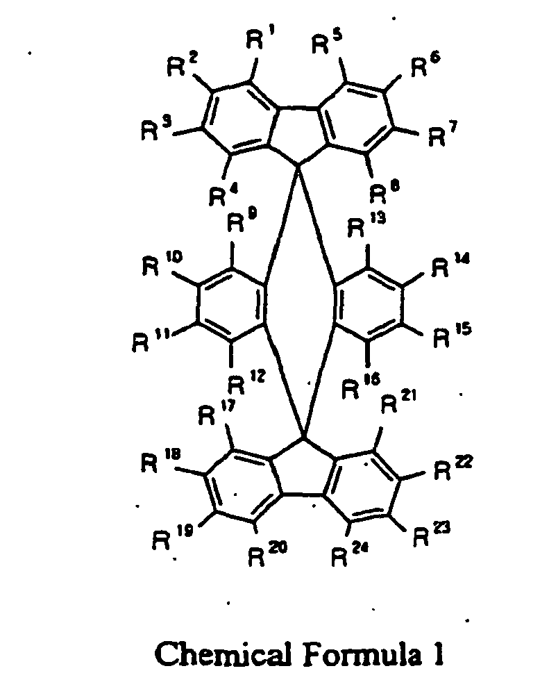
- The organic EL device of Claim 1, wherein one or more of the R1-R24 are aryl groups selected from phenyl, biphenyl, terphenyl, benzyl, naphthyl, anthracyl, tetracenyl, pentacenyl, perylenyl, coronenyl; and heteroaryl, which are either substituted or unsubstituted.
- The organic EL device of Claim 2, wherein the aryl groups are further substituted with one or more of phenyl, biphenyl, terphenyl, benzyl, naphthyl, anthracyl, tetracenyl, pentacenyl, perylenyl, coronenyl or heteroaryl, which are either substituted or unsubstituted.
- The organic EL device of Claim 1, wherein one or more of the R1-R24 are selected from a heteroaryl group consisting of thiophenyl, thiazolyl, oxazolyl, imidazolyl, and pyrazinyl, either substituted or unsubstituted.
- The organic EL device of Claim 1, wherein one or more of R1-R24 are selected from the group consisting of amines with at least one aryl substituent and aryl, wherein the aryl group is selected from phenyl, biphenyl, terphenyl, benzyl, naphthyl, anthracyl, tetracenyl, pentacenyl, perylenyl, coronenyl and heteroaryl.
- The organic EL device of Claim 1, wherein at least one of R1-R24 is anthracene or heteroaryl.
- The organic EL device of Claim 1, wherein the substituent groups R1 through R24 are substituted by one or more organic moieties satisfying Chemical Formula I.
- The organic EL device of Claim 1, wherein one or more of the R3, R7, R10, R11, R14, R15, R18, and R22 are substituted with non-hydrogen substituent groups.
- The organic EL device of Claim 1, wherein one or more pairs of R3 and R7; R18 and R22; R10 and R15; and R11 and R14 are substituted with non-hydrogen substituent groups.
- The organic EL device of Claim 1, wherein the light-emitting layer comprises the one or more double-spiro compounds halving, the band gap corresponding to visible light emission.
- The organic EL device of Claim 10, wherein the band-gap for the visible light emission is from 1.8 eV to 3.5 eV.
- The organic EL device of Claim 1, wherein the light-emitting layer further comprises one or more fluorescent or phosphorescent materials.
- The organic EL device of Claim 1, wherein the organic EL device is supported by a substrate, and wherein the substrate contacts either the anode or the cathode.
- The organic EL device of Claim 1, wherein at least one layer further comprises at least one material having one or more properties selected from the group consisting of electron injection, electron transportation, light emission, hole transportation, and hole injection.
- The organic EL device of Claim 1, wherein the light-emitting layer comprises one or more compounds selected from the group consisting of Chemical Compounds 100-137,200-222, and 400-413 as shown below:
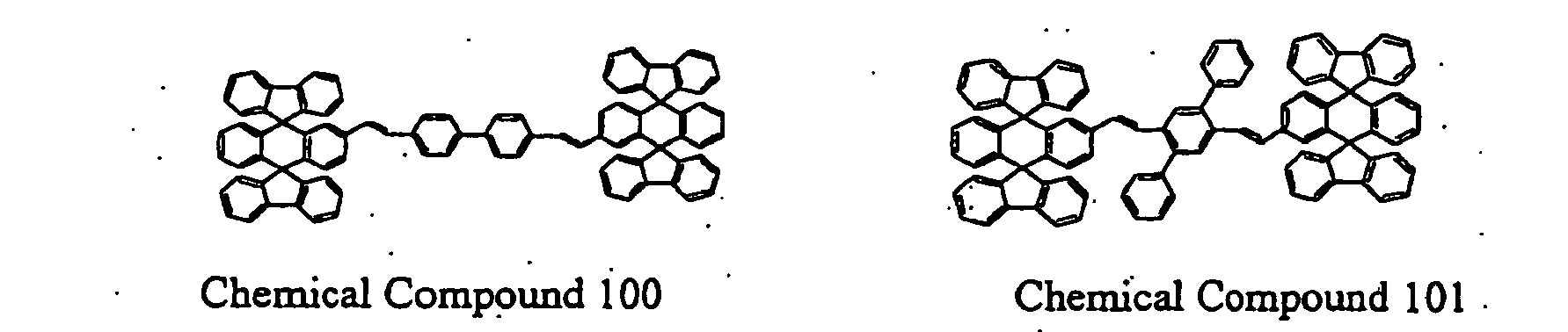
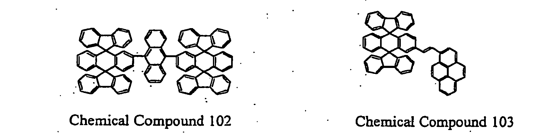


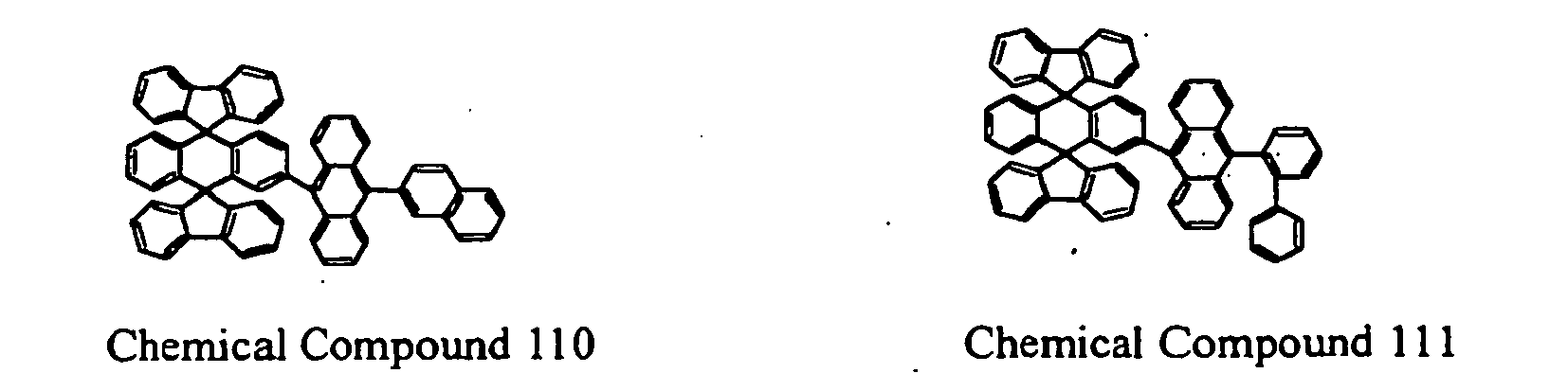

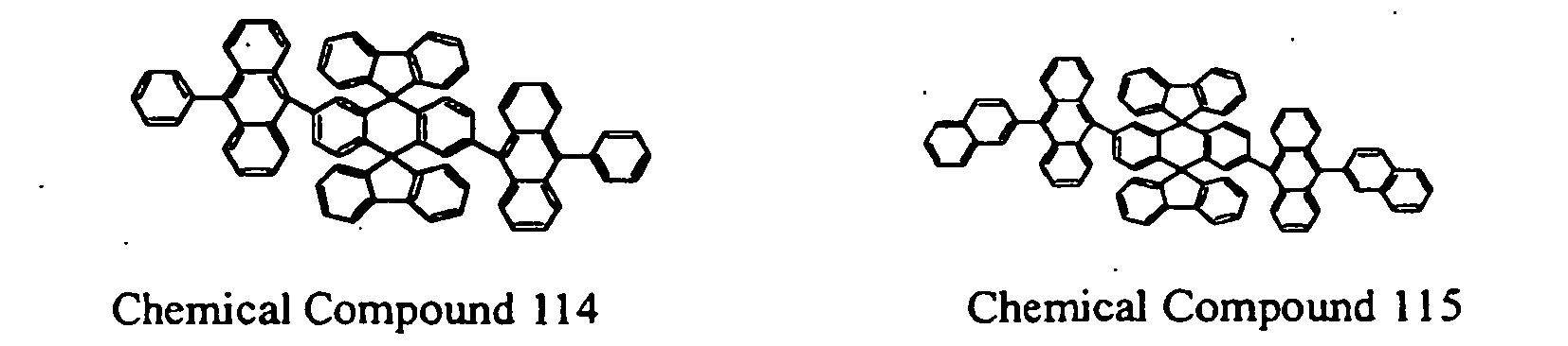
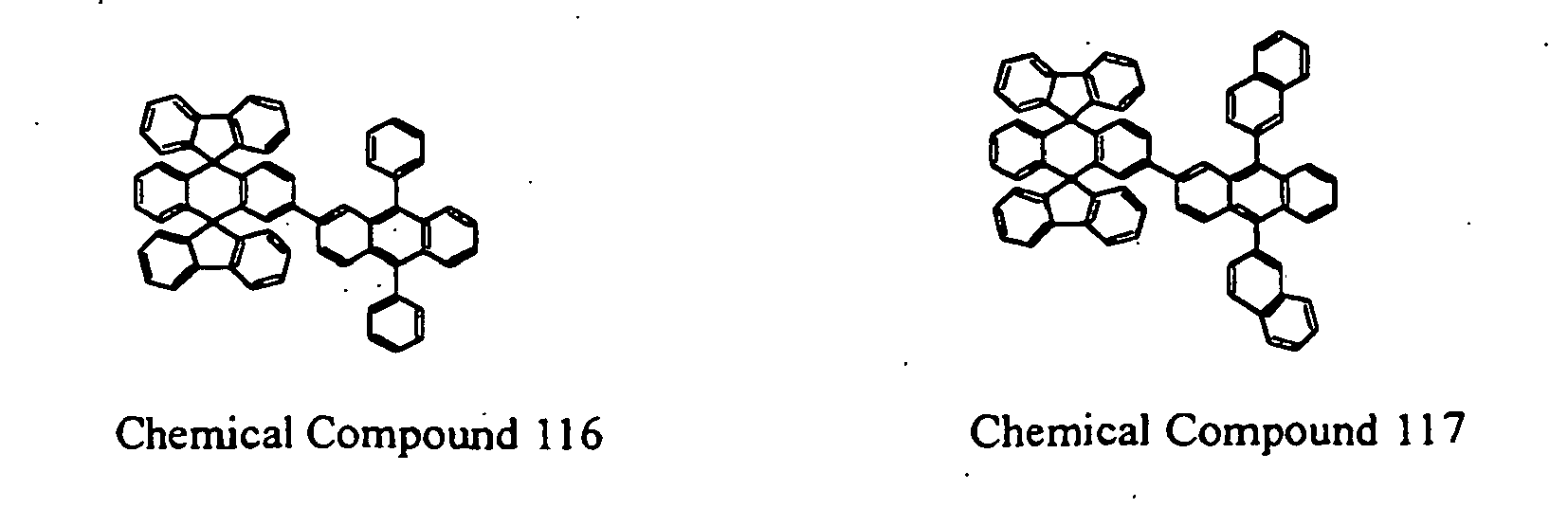


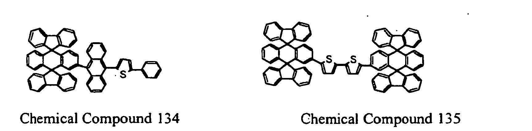


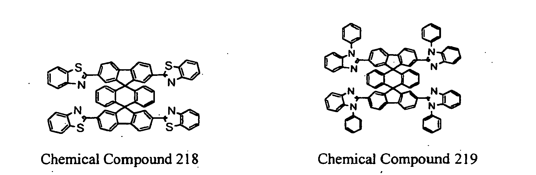

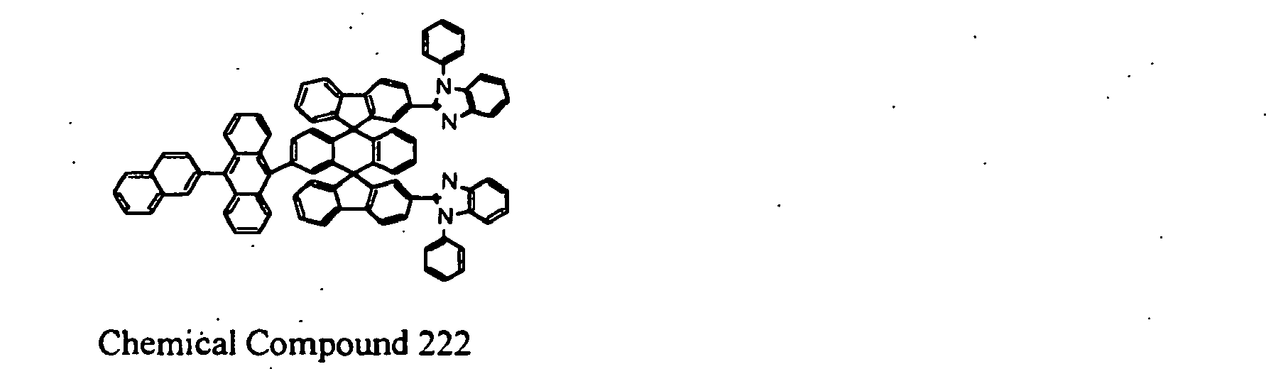
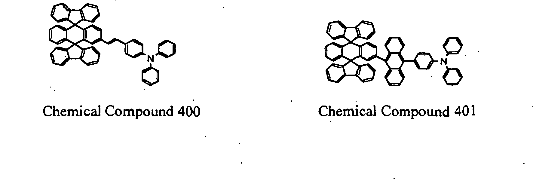


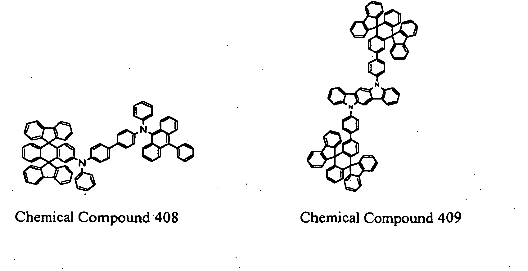

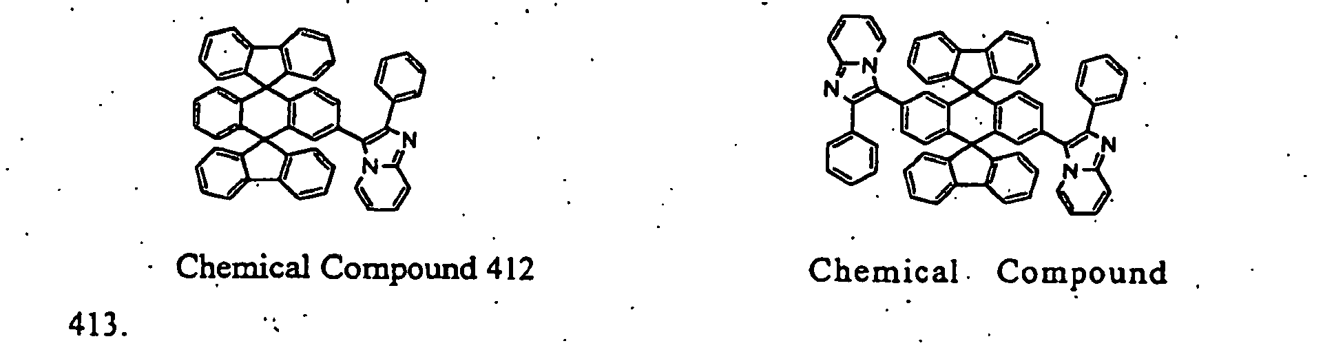
- The organic EL device of Claim 1, wherein the light-emitting layer further comprises one or more non-double-spiro light-emitting compounds.
- The organic EL device of Claim 16, wherein the non-double-spiro light-emitting compound has the band gap smaller than the band gap of the double-spiro compound.
- The organic EL device of Claim 16, wherein the non-double-spiro light-emitting compound has the band gap greater than the band gap of the double-spiro compound.
- The organic EL device of Claim 16, wherein the non-double-spiro light-emitting compound is either fluorescent or phosphorescent compounds.
- The organic EL device of Claim 1, wherein at least one layer further comprises at least one layer selected from the group consisting of the electron-injecting and electron-transporting layers.
- The organic EL device of Claim 20, wherein the at least one of the electron-injecting and electron-transporting layers comprises one or more compounds selected from the group consisting of Chemical Compounds 200-222 of claim 15 as shown below:
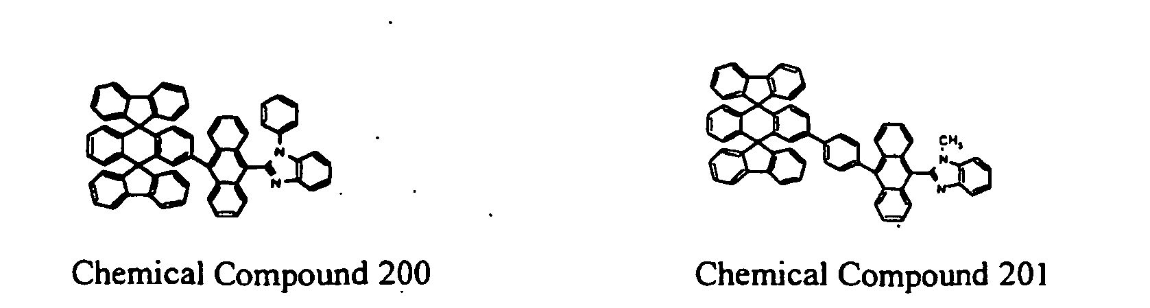

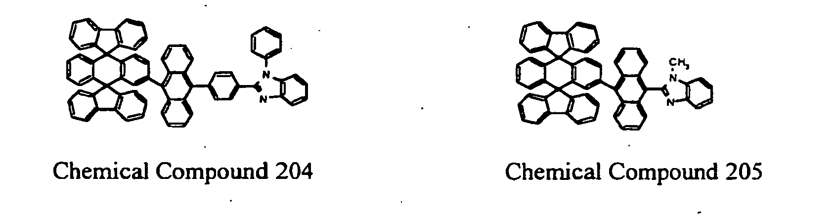
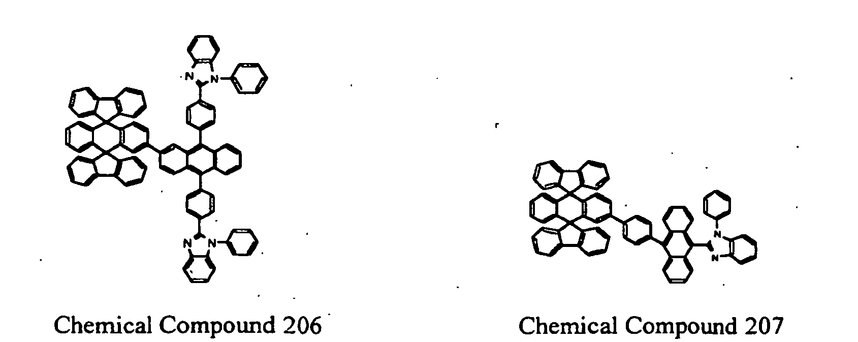


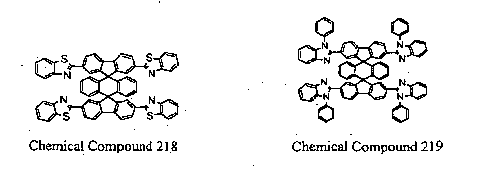


- The organic EL device of Claim 1, wherein at least one layer further comprises at least one layer selected from the group consisting of the hole-injecting and hole-transporting layers.
- The organic EL device of Claim 22, wherein the at least one of the hole-injecting and hole-transporting layers comprises one or more compounds selected from the group consisting of Chemical Compounds 300-308 and 400-413 of claim 15 as shown below:
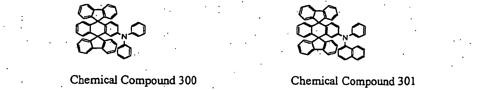
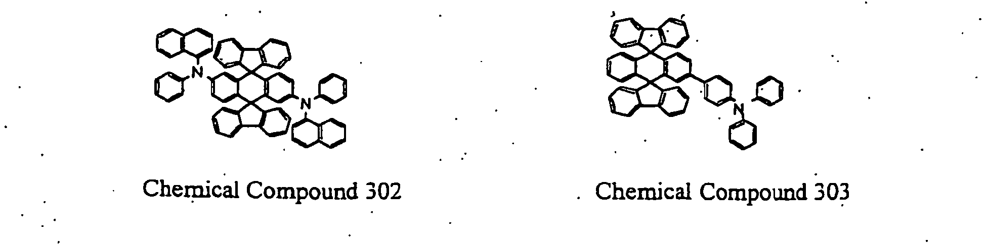


- An electronic device comprising a display having the organic EL device of Claim 1.
Applications Claiming Priority (3)
| Application Number | Priority Date | Filing Date | Title |
|---|---|---|---|
| KR10-2001-0023038A KR100428642B1 (en) | 2001-04-27 | 2001-04-27 | Organic material having double spiro structure |
| KR10-2001-0023039A KR100422914B1 (en) | 2001-04-27 | 2001-04-27 | Electronic device comprising organic material having double spiro structure |
| EP02705589A EP1294823B1 (en) | 2001-04-27 | 2002-03-18 | Double-spiro organic compounds and electroluminescent devices |
Related Parent Applications (2)
| Application Number | Title | Priority Date | Filing Date |
|---|---|---|---|
| EP02705589.6 Division | 2002-03-18 | ||
| EP02705589A Division EP1294823B1 (en) | 2001-04-27 | 2002-03-18 | Double-spiro organic compounds and electroluminescent devices |
Publications (2)
| Publication Number | Publication Date |
|---|---|
| EP1645552A1 EP1645552A1 (en) | 2006-04-12 |
| EP1645552B1 true EP1645552B1 (en) | 2010-05-05 |
Family
ID=26639032
Family Applications (2)
| Application Number | Title | Priority Date | Filing Date |
|---|---|---|---|
| EP02705589A Expired - Lifetime EP1294823B1 (en) | 2001-04-27 | 2002-03-18 | Double-spiro organic compounds and electroluminescent devices |
| EP05020697A Expired - Lifetime EP1645552B1 (en) | 2001-04-27 | 2002-03-18 | Electroluminescent devices made with double-spiro organic compounds |
Family Applications Before (1)
| Application Number | Title | Priority Date | Filing Date |
|---|---|---|---|
| EP02705589A Expired - Lifetime EP1294823B1 (en) | 2001-04-27 | 2002-03-18 | Double-spiro organic compounds and electroluminescent devices |
Country Status (9)
| Country | Link |
|---|---|
| US (2) | US6998487B2 (en) |
| EP (2) | EP1294823B1 (en) |
| JP (1) | JP3971310B2 (en) |
| CN (1) | CN100488923C (en) |
| AT (2) | ATE348136T1 (en) |
| DE (2) | DE60236329D1 (en) |
| ES (1) | ES2274003T3 (en) |
| TW (1) | TW591096B (en) |
| WO (1) | WO2002088274A1 (en) |
Families Citing this family (165)
| Publication number | Priority date | Publication date | Assignee | Title |
|---|---|---|---|---|
| KR100721656B1 (en) * | 2005-11-01 | 2007-05-23 | 주식회사 엘지화학 | Organic electrical devices |
| KR100377321B1 (en) * | 1999-12-31 | 2003-03-26 | 주식회사 엘지화학 | Electronic device comprising organic compound having p-type semiconducting characteristics |
| US7560175B2 (en) * | 1999-12-31 | 2009-07-14 | Lg Chem, Ltd. | Electroluminescent devices with low work function anode |
| JP4972844B2 (en) * | 2001-03-30 | 2012-07-11 | コニカミノルタホールディングス株式会社 | Organic electroluminescence device |
| US6855438B2 (en) * | 2001-06-15 | 2005-02-15 | Konica Corporation | Organic electroluminescent element and full color display |
| JP4089331B2 (en) * | 2001-07-25 | 2008-05-28 | 東レ株式会社 | Light emitting element |
| KR100691543B1 (en) * | 2002-01-18 | 2007-03-09 | 주식회사 엘지화학 | New material for electron transport and organic light emitting device using the same |
| JP4646494B2 (en) * | 2002-04-11 | 2011-03-09 | 出光興産株式会社 | Novel nitrogen-containing heterocyclic derivative and organic electroluminescence device using the same |
| AU2003230308A1 (en) | 2002-05-07 | 2003-11-11 | Lg Chem, Ltd. | New organic compounds for electroluminescence and organic electroluminescent devices using the same |
| US7265378B2 (en) | 2002-07-10 | 2007-09-04 | E. I. Du Pont De Nemours And Company | Electronic devices made with electron transport and/or anti-quenching layers |
| ATE529494T1 (en) * | 2002-07-19 | 2011-11-15 | Idemitsu Kosan Co | ORGANIC ELECTROLUMINescent DEVICES AND ORGANIC LIGHT EMITTING MEDIUM |
| KR100497532B1 (en) * | 2002-08-16 | 2005-07-01 | 네오뷰코오롱 주식회사 | Luminescent spiro dimer and organic light-emitting device comprising the same |
| US7839074B2 (en) | 2002-08-23 | 2010-11-23 | Idemitsu Kosan Co., Ltd. | Organic electroluminescence device and anthracene derivative |
| JP4045932B2 (en) * | 2002-11-21 | 2008-02-13 | コニカミノルタホールディングス株式会社 | Organic electroluminescence element and display device |
| EP2248870B1 (en) * | 2002-11-26 | 2018-12-26 | Konica Minolta Holdings, Inc. | Organic electroluminscent element and display and illuminator |
| JP4693336B2 (en) * | 2003-01-14 | 2011-06-01 | 出光興産株式会社 | Nitrogen-containing heterocyclic derivative and organic electroluminescence device using the same |
| EP1582516B1 (en) * | 2003-01-10 | 2013-07-17 | Idemitsu Kosan Co., Ltd. | Nitrogenous heterocyclic derivative and organic electroluminescent element employing the same |
| KR20040072004A (en) * | 2003-02-07 | 2004-08-16 | 삼성에스디아이 주식회사 | Emitting compound for electroluminescence device and device using thereof |
| EP2174932B1 (en) * | 2003-03-13 | 2019-07-03 | Idemitsu Kosan Co., Ltd. | Nitrogen-containing heterocycle derivative and organic electroluminescent element using the same |
| JP2004339136A (en) * | 2003-05-15 | 2004-12-02 | Idemitsu Kosan Co Ltd | Spiro bond-containing compound, luminescent coating material, and organic electroluminescent device using the same |
| KR100808790B1 (en) | 2003-05-23 | 2008-03-03 | 주식회사 엘지화학 | ITO film treated with nitrogen plasma and organic light emitting device using the same as anode |
| JP4481930B2 (en) | 2003-07-11 | 2010-06-16 | 出光興産株式会社 | White organic electroluminescence device |
| DE10339772B4 (en) | 2003-08-27 | 2006-07-13 | Novaled Gmbh | Light emitting device and method for its production |
| CN100335462C (en) * | 2003-09-05 | 2007-09-05 | 清华大学 | Carbazole derivative and its application in electroluminescent device |
| US9034482B2 (en) * | 2003-09-19 | 2015-05-19 | Merck Patent Gmbh | Organic electroluminescent element |
| JP4390113B2 (en) * | 2003-11-10 | 2009-12-24 | ケンブリッジ ディスプレイ テクノロジー リミテッド | Dibenzosilol polymer and method for producing the same |
| KR20070029122A (en) * | 2003-11-26 | 2007-03-13 | 시바 스페셜티 케미칼스 홀딩 인크. | Electroluminescent device comprising 2- (VII-triphenyl) -3-phenyl-pyrazine derivative |
| WO2005061657A1 (en) * | 2003-12-24 | 2005-07-07 | Mitsubishi Heavy Industries, Ltd. | Single-layer organic el device |
| TWI428053B (en) * | 2004-02-09 | 2014-02-21 | Idemitsu Kosan Co | Organic electroluminescent element |
| US7252893B2 (en) | 2004-02-17 | 2007-08-07 | Eastman Kodak Company | Anthracene derivative host having ranges of dopants |
| US7326371B2 (en) * | 2004-03-25 | 2008-02-05 | Eastman Kodak Company | Electroluminescent device with anthracene derivative host |
| US20080036365A1 (en) * | 2004-03-26 | 2008-02-14 | Hodogaya Chemical Co., Ltd. | Carbazole Derivative Containing Fluorene Group and Organic Electroluminescent Element |
| CN100508238C (en) | 2004-05-11 | 2009-07-01 | Lg化学株式会社 | Organic electronic device |
| KR100696470B1 (en) * | 2004-06-15 | 2007-03-19 | 삼성에스디아이 주식회사 | Organic electroluminescent element |
| JP2006028054A (en) * | 2004-07-14 | 2006-02-02 | Konica Minolta Holdings Inc | Organic thin film transistor material, organic thin film transistor, field effect transistor and switching element |
| US20060019116A1 (en) * | 2004-07-22 | 2006-01-26 | Eastman Kodak Company | White electroluminescent device with anthracene derivative host |
| EP1794255B1 (en) * | 2004-08-19 | 2016-11-16 | LG Chem, Ltd. | Organic light-emitting device comprising buffer layer and method for fabricating the same |
| US7683532B2 (en) * | 2004-11-02 | 2010-03-23 | Semiconductor Energy Laboratory Co., Ltd. | Semiconductor device and light emitting device |
| KR100708655B1 (en) * | 2004-11-27 | 2007-04-18 | 삼성에스디아이 주식회사 | Organic electroluminescent element |
| KR100669790B1 (en) * | 2004-11-27 | 2007-01-16 | 삼성에스디아이 주식회사 | Organic electroluminescent element |
| CN101894917B (en) * | 2004-12-06 | 2012-08-29 | 株式会社半导体能源研究所 | Light-emitting element and light-emitting device using the same |
| WO2006073059A1 (en) | 2005-01-05 | 2006-07-13 | Idemitsu Kosan Co., Ltd. | Aromatic amine derivative and organic electroluminescent device using same |
| JP4235619B2 (en) * | 2005-02-14 | 2009-03-11 | キヤノン株式会社 | Manufacturing method of organic light emitting device |
| US20060204783A1 (en) * | 2005-03-10 | 2006-09-14 | Conley Scott R | Organic electroluminescent device |
| KR101356093B1 (en) | 2005-03-28 | 2014-01-27 | 가부시키가이샤 한도오따이 에네루기 켄큐쇼 | Anthracene derivative, material for light emitting element, light emitting element, light emitting device, and electronic device |
| US20060269782A1 (en) * | 2005-05-25 | 2006-11-30 | Eastman Kodak Company | OLED electron-transporting layer |
| WO2006130598A2 (en) * | 2005-05-31 | 2006-12-07 | Universal Display Corporation | Triphenylene hosts in phosphorescent light emitting diodes |
| US20070003785A1 (en) * | 2005-06-30 | 2007-01-04 | Eastman Kodak Company | Electroluminescent devices containing benzidine derivatives |
| US8187727B2 (en) * | 2005-07-22 | 2012-05-29 | Lg Chem, Ltd. | Imidazole derivatives, preparation method thereof and organic electronic device using the same |
| WO2007026626A1 (en) * | 2005-08-31 | 2007-03-08 | Semiconductor Energy Laboratory Co., Ltd. | Carbazole derivative, material for light emitting element, light emitting element, light emitting device, and electronic device |
| JP5661982B2 (en) * | 2005-09-14 | 2015-01-28 | 住友化学株式会社 | Polymer compound, light emitting material, and light emitting device |
| US7915809B2 (en) * | 2005-10-07 | 2011-03-29 | Dow Corning Corporation | Electrophosphorescent organic light emitting diode formed using solvent soluble materials |
| KR100890862B1 (en) * | 2005-11-07 | 2009-03-27 | 주식회사 엘지화학 | Organic electroluminescent device and method for preparing the same |
| US9666826B2 (en) * | 2005-11-30 | 2017-05-30 | Global Oled Technology Llc | Electroluminescent device including an anthracene derivative |
| KR100864364B1 (en) * | 2005-12-13 | 2008-10-17 | 주식회사 엘지화학 | Novel imidazoquinazoline derivative, process for preparing the same, and organic electronic device using the same |
| US20070141393A1 (en) * | 2005-12-21 | 2007-06-21 | Eastman Kodak Company | Amino anthracene compounds in OLED devices |
| EP1971664B1 (en) * | 2006-01-13 | 2015-09-09 | LG Chem, Ltd. | Emitting materials and organic light emitting device using the same |
| US8680693B2 (en) * | 2006-01-18 | 2014-03-25 | Lg Chem. Ltd. | OLED having stacked organic light-emitting units |
| US7731377B2 (en) * | 2006-03-21 | 2010-06-08 | Semiconductor Energy Laboratory Co., Ltd. | Backlight device and display device |
| US20070252515A1 (en) * | 2006-04-27 | 2007-11-01 | Eastman Kodak Company | Electroluminescent device including an anthracene derivative |
| US7582508B2 (en) * | 2006-05-31 | 2009-09-01 | Byoung-Choo Park | Method for manufacturing an organic semiconductor device that utilizes ionic salt |
| WO2007139124A1 (en) * | 2006-06-01 | 2007-12-06 | Semiconductor Energy Laboratory Co., Ltd. | Light-emitting element, light-emitting device and an electronic device |
| CN101506163B (en) * | 2006-08-30 | 2012-05-02 | 株式会社半导体能源研究所 | Method for synthesizing anthracene derivative and anthracene derivative, light emitting element, light emitting device, electronic device |
| JP4979333B2 (en) * | 2006-10-13 | 2012-07-18 | 三井化学株式会社 | Anthracene compound and organic electroluminescence device containing the compound |
| KR100898073B1 (en) * | 2006-11-22 | 2009-05-18 | 삼성모바일디스플레이주식회사 | Quinoxaline ring-containing compound and organic light emitting device using the same |
| KR100925323B1 (en) * | 2006-12-01 | 2009-11-04 | 주식회사 엘지화학 | Novel compound and organic light emitting device using same |
| US9397308B2 (en) * | 2006-12-04 | 2016-07-19 | Semiconductor Energy Laboratory Co., Ltd. | Light emitting element, light emitting device, and electronic device |
| WO2008069153A1 (en) | 2006-12-04 | 2008-06-12 | Semiconductor Energy Laboratory Co., Ltd. | Light-emitting element, light-emitting device, and electronic device |
| US7723722B2 (en) | 2007-03-23 | 2010-05-25 | Semiconductor Energy Laboratory Co., Ltd. | Organic compound, anthracene derivative, and light-emitting element, light-emitting device, and electronic device using anthracene derivative |
| KR100857026B1 (en) * | 2007-03-28 | 2008-09-05 | (주)그라쎌 | Thiazole organic light emitting compound and organic light emitting device comprising the same |
| US20080286445A1 (en) * | 2007-05-17 | 2008-11-20 | Semiconductor Energy Laboratory Co., Ltd. | Composition, and method of fabricating light-emitting element |
| JP5484690B2 (en) * | 2007-05-18 | 2014-05-07 | ユー・ディー・シー アイルランド リミテッド | Organic electroluminescence device |
| KR101030007B1 (en) * | 2007-06-15 | 2011-04-20 | 삼성모바일디스플레이주식회사 | Heteroaromatic cycle containing compound method of preparing the same and an organic light emitting device comprising the same |
| US20090045731A1 (en) * | 2007-07-07 | 2009-02-19 | Idemitsu Kosan Co., Ltd. | Organic electroluminescence device and material for organic electroluminescence device |
| US20090091242A1 (en) * | 2007-10-05 | 2009-04-09 | Liang-Sheng Liao | Hole-injecting layer in oleds |
| TWI479712B (en) | 2007-10-19 | 2015-04-01 | Semiconductor Energy Lab | Light-emitting device |
| EP2075308A3 (en) * | 2007-12-25 | 2010-04-14 | Yamagata Promotional Organization for Industrial Technology | organic electroluminescence material and element using the same |
| EP2236485A1 (en) * | 2007-12-25 | 2010-10-06 | National University Corporation Nagoya University | Organic material containing oligophenylene skeleton and light-emitting device using the same |
| CN101978784B (en) | 2008-03-18 | 2012-12-05 | 株式会社半导体能源研究所 | Light emitting element, light emitting device and electronic device |
| WO2009116547A1 (en) * | 2008-03-18 | 2009-09-24 | Semiconductor Energy Laboratory Co., Ltd. | Light-emitting element, light-emitting device and electronic device |
| JP5611538B2 (en) * | 2008-05-16 | 2014-10-22 | 株式会社半導体エネルギー研究所 | Benzoxazole derivative, and light-emitting element, light-emitting device, lighting device, and electronic device using benzoxazole derivative |
| KR101913462B1 (en) * | 2008-06-30 | 2018-10-30 | 유니버셜 디스플레이 코포레이션 | Hole transport materials having a sulfer-containing group |
| CN102089282A (en) * | 2008-07-08 | 2011-06-08 | 株式会社半导体能源研究所 | Carbazole derivative, light-emitting element material, light-emitting element, and light-emitting device |
| DE102008036982A1 (en) * | 2008-08-08 | 2010-02-11 | Merck Patent Gmbh | Organic electroluminescent device |
| EP2166001B1 (en) * | 2008-09-19 | 2011-07-20 | Semiconductor Energy Laboratory Co., Ltd. | Carbazole Derivative and Method for Producing the Same |
| KR101333697B1 (en) | 2008-10-14 | 2013-11-27 | 제일모직주식회사 | benzimidazole compounds and organic photoelectric device with the same |
| WO2010061315A1 (en) * | 2008-11-26 | 2010-06-03 | Philips Intellectual Property & Standards Gmbh | Oled with novel hole-conducting material |
| EP2200407B1 (en) * | 2008-12-17 | 2017-11-22 | Semiconductor Energy Laboratory Co., Ltd. | Light-Emitting element, light emitting device, and electronic device |
| EP2372803A4 (en) * | 2008-12-26 | 2012-07-04 | Idemitsu Kosan Co | MATERIAL FOR ORGANIC ELECTROLUMINESCENT ELEMENT, AND ORGANIC ELECTROLUMINESCENT ELEMENT |
| TWI583253B (en) * | 2009-01-21 | 2017-05-11 | 半導體能源研究所股份有限公司 | Light-emitting element, light-emitting device and electronic device |
| CN102482575B (en) * | 2009-09-10 | 2015-01-21 | 株式会社Lg化学 | New heterocyclic derivatives and organic electroluminescent devices using them |
| JPWO2011043083A1 (en) * | 2009-10-09 | 2013-03-04 | 出光興産株式会社 | Organic electroluminescence device |
| KR101847222B1 (en) * | 2009-10-23 | 2018-04-09 | 호도가야 가가쿠 고교 가부시키가이샤 | Organic electroluminescent element |
| JP5697599B2 (en) * | 2009-10-23 | 2015-04-08 | 新日鉄住金化学株式会社 | Organic electroluminescence device |
| WO2011048822A1 (en) * | 2009-10-23 | 2011-04-28 | 保土谷化学工業株式会社 | Organic electroluminescent element |
| DE102009051172A1 (en) * | 2009-10-29 | 2011-05-05 | Merck Patent Gmbh | Materials for electronic devices |
| JP5578832B2 (en) * | 2009-11-05 | 2014-08-27 | キヤノン株式会社 | Novel fluorenylamine compound and organic light emitting device having the same |
| US8617720B2 (en) * | 2009-12-21 | 2013-12-31 | E I Du Pont De Nemours And Company | Electroactive composition and electronic device made with the composition |
| US8617724B2 (en) * | 2010-01-28 | 2013-12-31 | Sumitomo Chemical Company, Limited | Polymer compound and light emitting device using the same |
| KR101769173B1 (en) | 2010-01-28 | 2017-08-17 | 스미또모 가가꾸 가부시키가이샤 | Polymer compound and light-emitting device using same |
| DE102010010481A1 (en) * | 2010-03-06 | 2011-09-08 | Merck Patent Gmbh | Organic electroluminescent device |
| TW201204687A (en) * | 2010-06-17 | 2012-02-01 | Du Pont | Electroactive materials |
| US20120049168A1 (en) * | 2010-08-31 | 2012-03-01 | Universal Display Corporation | Cross-Linked Charge Transport Layer Containing an Additive Compound |
| KR101670964B1 (en) * | 2010-12-13 | 2016-11-09 | 삼성전자주식회사 | Polymer and organic light emitting diode comprising the same |
| JP5756288B2 (en) * | 2010-12-28 | 2015-07-29 | 出光興産株式会社 | Fused polycyclic compound, material for organic electroluminescence device, and organic electroluminescence device using the same |
| CN103430344B (en) * | 2011-03-14 | 2016-03-23 | 东丽株式会社 | Light emitting element material and light-emitting component |
| JP5868195B2 (en) * | 2011-04-14 | 2016-02-24 | キヤノン株式会社 | Novel spiro compound and organic light emitting device having the same |
| JP6022541B2 (en) * | 2011-04-18 | 2016-11-09 | メルク パテント ゲーエムベーハー | Compounds for electronic devices |
| JP5721533B2 (en) * | 2011-05-18 | 2015-05-20 | キヤノン株式会社 | Dispirodibenzonaphthacene compound and organic light-emitting device using the same |
| US9403795B2 (en) * | 2011-08-05 | 2016-08-02 | Samsung Display Co., Ltd. | Carbazole-based compound and organic light-emitting diode comprising the same |
| JP5899010B2 (en) * | 2012-03-06 | 2016-04-06 | 株式会社ダイセル | ANANTHOLENE COMPOUND AND PROCESS FOR PRODUCING THE SAME |
| DE102012011335A1 (en) * | 2012-06-06 | 2013-12-12 | Merck Patent Gmbh | Connections for Organic Electronic Devices |
| DE112013007830B4 (en) | 2012-08-03 | 2024-07-04 | Semiconductor Energy Laboratory Co., Ltd. | Light-emitting element, light-emitting device and lighting device |
| US9209411B2 (en) | 2012-12-07 | 2015-12-08 | Universal Display Corporation | Organic electroluminescent materials and devices |
| US9478749B2 (en) * | 2013-03-28 | 2016-10-25 | Semiconductor Energy Laboratory Co., Ltd. | Anthracene compound, light-emitting element, light-emitting device, electronic appliance, and lighting device |
| US9537106B2 (en) * | 2013-05-09 | 2017-01-03 | Universal Display Corporation | Organic electroluminescent materials and devices |
| US9224958B2 (en) * | 2013-07-19 | 2015-12-29 | Universal Display Corporation | Organic electroluminescent materials and devices |
| US10593886B2 (en) * | 2013-08-25 | 2020-03-17 | Molecular Glasses, Inc. | OLED devices with improved lifetime using non-crystallizable molecular glass mixture hosts |
| WO2015086108A1 (en) * | 2013-12-12 | 2015-06-18 | Merck Patent Gmbh | Materials for electronic devices |
| KR20150077269A (en) | 2013-12-27 | 2015-07-07 | 삼성디스플레이 주식회사 | Organic electroluminescence device |
| JP6177124B2 (en) * | 2013-12-27 | 2017-08-09 | 株式会社半導体エネルギー研究所 | Organic compound, light emitting element, light emitting device, display device, lighting device, and electronic device |
| JP6230904B2 (en) * | 2013-12-27 | 2017-11-15 | 株式会社半導体エネルギー研究所 | Organic compounds, light emitting devices |
| JP2016086147A (en) * | 2014-10-29 | 2016-05-19 | 保土谷化学工業株式会社 | Organic electroluminescence device |
| US11158811B2 (en) * | 2014-12-05 | 2021-10-26 | Hodogaya Chemical Co., Ltd. | Organic electroluminescent device |
| US10593884B2 (en) * | 2015-01-06 | 2020-03-17 | Hodogaya Chemical Co., Ltd. | Organic electroluminescent device |
| EP3244463B1 (en) * | 2015-01-08 | 2020-07-22 | Hodogaya Chemical Co., Ltd. | Organic electroluminescent device |
| KR101837804B1 (en) * | 2015-02-16 | 2018-03-12 | 주식회사 엘지화학 | Double spiro structure compound and organic light emitting device comprising the same |
| US10403826B2 (en) * | 2015-05-07 | 2019-09-03 | Universal Display Corporation | Organic electroluminescent materials and devices |
| KR101826427B1 (en) * | 2015-06-05 | 2018-02-06 | 주식회사 엘지화학 | Organic compound having double spiro structure and organic electronic device comprising the same |
| WO2017007213A2 (en) * | 2015-07-07 | 2017-01-12 | 주식회사 엘지화학 | Double spiro compound and organic light-emitting element comprising same |
| GB201513037D0 (en) * | 2015-07-23 | 2015-09-09 | Merck Patent Gmbh | Phenyl-derived compound for use in organic electronic devices |
| EP3138858B1 (en) * | 2015-09-01 | 2019-10-30 | Samsung Electronics Co., Ltd. | Amino fluorene polymer and organic light-emitting device including the same |
| WO2017061788A1 (en) * | 2015-10-06 | 2017-04-13 | 주식회사 엘지화학 | Spiro compound and organic light-emitting device comprising same |
| KR102065818B1 (en) | 2015-10-06 | 2020-01-13 | 주식회사 엘지화학 | Spiro structure compound and organic light emitting device comprising the same |
| KR101991049B1 (en) | 2015-10-06 | 2019-06-20 | 주식회사 엘지화학 | Spiro structure compound and organic light emitting device comprising the same |
| KR101991050B1 (en) | 2015-10-06 | 2019-06-20 | 주식회사 엘지화학 | Spiro structure compound and organic light emitting device comprising the same |
| WO2017061786A1 (en) * | 2015-10-06 | 2017-04-13 | 주식회사 엘지화학 | Spiro compound and organic light-emitting device comprising same |
| KR101985649B1 (en) | 2015-10-07 | 2019-06-04 | 주식회사 엘지화학 | Double spiro structured compound and organic light emitting device comprising the same |
| KR102000177B1 (en) * | 2015-10-26 | 2019-07-16 | 주식회사 엘지화학 | Compound having spiro structure and organic light emitting device comprising the same |
| US11594683B2 (en) | 2015-10-29 | 2023-02-28 | Hodogaya Chemical Co., Ltd. | Organic electroluminescent device |
| WO2017122813A1 (en) * | 2016-01-14 | 2017-07-20 | 保土谷化学工業株式会社 | Organic electroluminescent element |
| KR102844041B1 (en) | 2016-02-26 | 2025-08-11 | 가부시키가이샤 한도오따이 에네루기 켄큐쇼 | Organic compound, light-emitting element, light-emitting device, electronic device, and lighting device |
| WO2018083801A1 (en) * | 2016-11-07 | 2018-05-11 | 日立化成株式会社 | Organic electronic material, organic layer, organic electronic element, organic electroluminescent element, display element, illumination device, and display device |
| WO2018095387A1 (en) * | 2016-11-23 | 2018-05-31 | 广州华睿光电材料有限公司 | Organic chemical compound and application thereof, organic mixture, and organic electronic component |
| US10490753B2 (en) * | 2016-12-15 | 2019-11-26 | Universal Display Corporation | Organic electroluminescent materials and devices |
| KR102649432B1 (en) * | 2016-12-29 | 2024-03-19 | 엘지디스플레이 주식회사 | Organic compounds, organic light emitting diode and organic light emitting device having the compounds |
| CN108264487A (en) * | 2016-12-30 | 2018-07-10 | 吉林奥来德光电材料股份有限公司 | A kind of novel glyoxaline compound and its application |
| EP3591727A4 (en) | 2017-03-02 | 2020-12-23 | Hitachi Chemical Co., Ltd. | ORGANIC ELECTRONIC MATERIAL AND USE THEREOF |
| CN108623594B (en) * | 2017-03-22 | 2019-09-17 | 中国科学院化学研究所 | A kind of loop coil aromatic condensed ring imide analog compounds and preparation method thereof |
| US11158820B2 (en) * | 2017-03-29 | 2021-10-26 | Universal Display Corporation | Organic electroluminescent materials and devices |
| US11608321B2 (en) * | 2017-06-23 | 2023-03-21 | Universal Display Corporation | Organic electroluminescent materials and devices |
| US10109803B1 (en) * | 2017-08-14 | 2018-10-23 | Idemitsu Kosan Co., Ltd. | Organic electroluminescence device and electronic device |
| KR20190049958A (en) * | 2017-10-30 | 2019-05-10 | 삼성디스플레이 주식회사 | Condensed-cyclic compound and organic light emitting device comprising the same |
| US11349081B2 (en) * | 2017-11-14 | 2022-05-31 | Beijing Summer Sprout Technology Co., Ltd. | Azaindolocarbazole compounds |
| KR102703716B1 (en) * | 2018-04-09 | 2024-09-06 | 삼성전자주식회사 | Condensed cyclic compound and organic light-emitting device including the same |
| CN108794404B (en) * | 2018-06-28 | 2020-08-21 | 吉林奥来德光电材料股份有限公司 | Anthracene organic luminescent compound, preparation method thereof and organic electroluminescent device |
| KR102575479B1 (en) * | 2018-07-31 | 2023-09-08 | 삼성디스플레이 주식회사 | Organic electroluminescence device and polycyclic compound for organic electroluminescence device |
| KR102895676B1 (en) * | 2018-11-08 | 2025-12-04 | 이데미쓰 고산 가부시키가이샤 | Novel compounds, organic electroluminescent devices, and electronic devices utilizing them |
| CN110845499B (en) * | 2018-12-10 | 2023-08-22 | 广州华睿光电材料有限公司 | Nitrogen-containing polycyclic compounds, polymers, mixtures, compositions and organic electronic devices |
| JP7397005B2 (en) * | 2018-12-25 | 2023-12-12 | 保土谷化学工業株式会社 | organic electroluminescent device |
| KR102661468B1 (en) * | 2019-02-15 | 2024-04-30 | 삼성디스플레이 주식회사 | Organic light emitting device and electronic apparatus comprising the same |
| KR102770946B1 (en) | 2019-04-12 | 2025-02-24 | 삼성디스플레이 주식회사 | Organic electroluminescence device and polycyclic compound for organic electroluminescence device |
| KR102908941B1 (en) | 2019-12-13 | 2026-01-09 | 삼성디스플레이 주식회사 | Organic electroluminescence device and fused polycyclic compound for organic electroluminescence device |
| KR102815486B1 (en) | 2020-01-17 | 2025-06-02 | 삼성디스플레이 주식회사 | Organic electroluminescence device and fused polycyclic compound for organic electroluminescence device |
| CN115960001B (en) * | 2022-10-24 | 2024-04-19 | 陕西莱特光电材料股份有限公司 | Organic compound, and electronic component and electronic device including the same |
Family Cites Families (10)
| Publication number | Priority date | Publication date | Assignee | Title |
|---|---|---|---|---|
| US3869363A (en) * | 1973-12-13 | 1975-03-04 | American Cyanamid Co | Generation of photofluorescent materials by short wavelength ultraviolet irradiation of non-fluorescent bis-diarylchloromethyl-1,3,4-oxadiazoles |
| US5026894A (en) * | 1990-03-12 | 1991-06-25 | University Of South Carolina | Compound for use in the synthesis of semiconducting polymers with perpendicularly arranged cores and method of synthesizing said compound |
| EP0676461B1 (en) * | 1994-04-07 | 2002-08-14 | Covion Organic Semiconductors GmbH | Spiro compounds and their application as electroluminescence materials |
| DE4436773A1 (en) * | 1994-10-14 | 1996-04-18 | Hoechst Ag | Conjugated polymers with spirocenters and their use as electroluminescent materials |
| CN1223065A (en) * | 1997-02-22 | 1999-07-14 | Lg化学株式会社 | Organometallic complexes for use in electroluminescent devices |
| DE19711714A1 (en) * | 1997-03-20 | 1998-10-01 | Hoechst Ag | Spiro compounds and their use |
| DE19711568A1 (en) * | 1997-03-20 | 1998-10-01 | Hoechst Ag | Spiro compounds and their use |
| JPH11273863A (en) | 1998-03-25 | 1999-10-08 | Toyota Central Res & Dev Lab Inc | Organic electroluminescent device |
| CN1157461C (en) * | 2001-08-20 | 2004-07-14 | 清华大学 | Double spiro derivatives and their applications as electroluminescent materials |
| AU2003230308A1 (en) * | 2002-05-07 | 2003-11-11 | Lg Chem, Ltd. | New organic compounds for electroluminescence and organic electroluminescent devices using the same |
-
2002
- 2002-03-14 US US10/099,781 patent/US6998487B2/en not_active Expired - Lifetime
- 2002-03-18 AT AT02705589T patent/ATE348136T1/en not_active IP Right Cessation
- 2002-03-18 EP EP02705589A patent/EP1294823B1/en not_active Expired - Lifetime
- 2002-03-18 ES ES02705589T patent/ES2274003T3/en not_active Expired - Lifetime
- 2002-03-18 CN CNB028013808A patent/CN100488923C/en not_active Expired - Lifetime
- 2002-03-18 JP JP2002585559A patent/JP3971310B2/en not_active Expired - Lifetime
- 2002-03-18 WO PCT/KR2002/000458 patent/WO2002088274A1/en not_active Ceased
- 2002-03-18 DE DE60236329T patent/DE60236329D1/en not_active Expired - Lifetime
- 2002-03-18 DE DE60216681T patent/DE60216681T2/en not_active Expired - Lifetime
- 2002-03-18 EP EP05020697A patent/EP1645552B1/en not_active Expired - Lifetime
- 2002-03-18 AT AT05020697T patent/ATE466828T1/en not_active IP Right Cessation
- 2002-03-26 TW TW091105844A patent/TW591096B/en not_active IP Right Cessation
-
2003
- 2003-11-19 US US10/718,083 patent/US6984462B2/en not_active Expired - Lifetime
Also Published As
| Publication number | Publication date |
|---|---|
| US6998487B2 (en) | 2006-02-14 |
| DE60216681D1 (en) | 2007-01-25 |
| CN100488923C (en) | 2009-05-20 |
| JP2004529937A (en) | 2004-09-30 |
| ATE466828T1 (en) | 2010-05-15 |
| ES2274003T3 (en) | 2007-05-16 |
| EP1645552A1 (en) | 2006-04-12 |
| DE60236329D1 (en) | 2010-06-17 |
| US20040023060A1 (en) | 2004-02-05 |
| ATE348136T1 (en) | 2007-01-15 |
| US6984462B2 (en) | 2006-01-10 |
| TW591096B (en) | 2004-06-11 |
| WO2002088274A1 (en) | 2002-11-07 |
| JP3971310B2 (en) | 2007-09-05 |
| DE60216681T2 (en) | 2007-10-11 |
| EP1294823A1 (en) | 2003-03-26 |
| US20040170863A1 (en) | 2004-09-02 |
| EP1294823B1 (en) | 2006-12-13 |
| CN1462303A (en) | 2003-12-17 |
Similar Documents
| Publication | Publication Date | Title |
|---|---|---|
| EP1645552B1 (en) | Electroluminescent devices made with double-spiro organic compounds | |
| US7485733B2 (en) | Organic compounds for electroluminescence and organic electroluminescent devices using the same | |
| KR101694492B1 (en) | Amine compound and organic electroluminescent device using the same | |
| KR101367514B1 (en) | New anthracene derivatives and organic electronic device using the same | |
| TWI478898B (en) | New diamine derivatives and organic electronic device using the same | |
| KR20160127429A (en) | An electroluminescent compound and an electroluminescent device comprising the same | |
| JP2011016807A (en) | New organic compound and organic luminescent element using the same | |
| KR20120083243A (en) | New compounds and organic electronic device using the same | |
| KR101396647B1 (en) | New anthracene derivatives, preparation method thereof and organic electronic device using the same | |
| EP1937789B1 (en) | Indene derivatives and organic light emitting diode using the same | |
| KR20150115225A (en) | An electroluminescent compound and an electroluminescent device comprising the same | |
| KR20150044592A (en) | Method of preparing amine compound | |
| JP7751160B2 (en) | Spirobifluorene compounds and organic electroluminescent devices | |
| KR101472057B1 (en) | An asymmetric anthracene derivatives, a method of making the same, and organic electroluminescent device using the same | |
| JP4406045B2 (en) | New organic light emitting compound and organic light emitting device using the same | |
| KR20140016214A (en) | New anthracene derivatives, preparation method thereof and organic electronic device using the same | |
| KR20160031468A (en) | Method of preparing amine compound | |
| TW201730147A (en) | Aromatic compound and organic light-emitting diode containing the same |
Legal Events
| Date | Code | Title | Description |
|---|---|---|---|
| PUAI | Public reference made under article 153(3) epc to a published international application that has entered the european phase |
Free format text: ORIGINAL CODE: 0009012 |
|
| AC | Divisional application: reference to earlier application |
Ref document number: 1294823 Country of ref document: EP Kind code of ref document: P |
|
| AK | Designated contracting states |
Kind code of ref document: A1 Designated state(s): AT BE CH CY DE DK ES FI FR GB GR IE IT LI LU MC NL PT SE TR |
|
| 17P | Request for examination filed |
Effective date: 20060529 |
|
| RIN1 | Information on inventor provided before grant (corrected) |
Inventor name: SON, SE-HWAN Inventor name: KIM, KONG-KYEUM Inventor name: BAE, JAE-SOON Inventor name: LEE, JAE-CHOL Inventor name: LEE, YOUN-GU Inventor name: IM, SUNG-GAP Inventor name: KIM, JI-EUN Inventor name: YOON, SEOK-HEE |
|
| 17Q | First examination report despatched |
Effective date: 20060703 |
|
| AKX | Designation fees paid |
Designated state(s): AT BE CH CY DE DK ES FI FR GB GR IE IT LI LU MC NL PT SE TR |
|
| GRAP | Despatch of communication of intention to grant a patent |
Free format text: ORIGINAL CODE: EPIDOSNIGR1 |
|
| RIC1 | Information provided on ipc code assigned before grant |
Ipc: C07D 487/04 20060101ALI20090820BHEP Ipc: C09K 11/06 20060101ALI20090820BHEP Ipc: C07D 409/10 20060101ALI20090820BHEP Ipc: C07D 333/08 20060101ALI20090820BHEP Ipc: C07C 25/22 20060101ALI20090820BHEP Ipc: C07C 17/35 20060101ALI20090820BHEP Ipc: C07C 47/546 20060101ALI20090820BHEP Ipc: C07D 209/88 20060101ALI20090820BHEP Ipc: H01L 51/50 20060101ALN20090820BHEP Ipc: C07D 277/66 20060101ALI20090820BHEP Ipc: C07C 211/54 20060101ALI20090820BHEP Ipc: C07D 209/86 20060101ALI20090820BHEP Ipc: C07C 13/72 20060101AFI20090820BHEP Ipc: C07D 519/00 20060101ALI20090820BHEP Ipc: C07D 241/42 20060101ALI20090820BHEP Ipc: C07C 211/61 20060101ALI20090820BHEP Ipc: C07D 263/56 20060101ALI20090820BHEP Ipc: C07D 471/04 20060101ALI20090820BHEP Ipc: C07D 235/18 20060101ALI20090820BHEP Ipc: C07F 5/02 20060101ALI20090820BHEP Ipc: C07D 333/18 20060101ALI20090820BHEP |
|
| RTI1 | Title (correction) |
Free format text: ELECTROLUMINESCENT DEVICES MADE WITH DOUBLE-SPIRO ORGANIC COMPOUNDS |
|
| GRAS | Grant fee paid |
Free format text: ORIGINAL CODE: EPIDOSNIGR3 |
|
| GRAA | (expected) grant |
Free format text: ORIGINAL CODE: 0009210 |
|
| AC | Divisional application: reference to earlier application |
Ref document number: 1294823 Country of ref document: EP Kind code of ref document: P |
|
| AK | Designated contracting states |
Kind code of ref document: B1 Designated state(s): AT BE CH CY DE DK ES FI FR GB GR IE IT LI LU MC NL PT SE TR |
|
| REG | Reference to a national code |
Ref country code: GB Ref legal event code: FG4D |
|
| REG | Reference to a national code |
Ref country code: CH Ref legal event code: EP |
|
| REG | Reference to a national code |
Ref country code: IE Ref legal event code: FG4D |
|
| REF | Corresponds to: |
Ref document number: 60236329 Country of ref document: DE Date of ref document: 20100617 Kind code of ref document: P |
|
| REG | Reference to a national code |
Ref country code: NL Ref legal event code: T3 |
|
| PG25 | Lapsed in a contracting state [announced via postgrant information from national office to epo] |
Ref country code: SE Free format text: LAPSE BECAUSE OF FAILURE TO SUBMIT A TRANSLATION OF THE DESCRIPTION OR TO PAY THE FEE WITHIN THE PRESCRIBED TIME-LIMIT Effective date: 20100505 Ref country code: ES Free format text: LAPSE BECAUSE OF FAILURE TO SUBMIT A TRANSLATION OF THE DESCRIPTION OR TO PAY THE FEE WITHIN THE PRESCRIBED TIME-LIMIT Effective date: 20100816 |
|
| PG25 | Lapsed in a contracting state [announced via postgrant information from national office to epo] |
Ref country code: FI Free format text: LAPSE BECAUSE OF FAILURE TO SUBMIT A TRANSLATION OF THE DESCRIPTION OR TO PAY THE FEE WITHIN THE PRESCRIBED TIME-LIMIT Effective date: 20100505 Ref country code: AT Free format text: LAPSE BECAUSE OF FAILURE TO SUBMIT A TRANSLATION OF THE DESCRIPTION OR TO PAY THE FEE WITHIN THE PRESCRIBED TIME-LIMIT Effective date: 20100505 |
|
| PG25 | Lapsed in a contracting state [announced via postgrant information from national office to epo] |
Ref country code: CY Free format text: LAPSE BECAUSE OF FAILURE TO SUBMIT A TRANSLATION OF THE DESCRIPTION OR TO PAY THE FEE WITHIN THE PRESCRIBED TIME-LIMIT Effective date: 20100505 Ref country code: GR Free format text: LAPSE BECAUSE OF FAILURE TO SUBMIT A TRANSLATION OF THE DESCRIPTION OR TO PAY THE FEE WITHIN THE PRESCRIBED TIME-LIMIT Effective date: 20100806 |
|
| PG25 | Lapsed in a contracting state [announced via postgrant information from national office to epo] |
Ref country code: DK Free format text: LAPSE BECAUSE OF FAILURE TO SUBMIT A TRANSLATION OF THE DESCRIPTION OR TO PAY THE FEE WITHIN THE PRESCRIBED TIME-LIMIT Effective date: 20100505 Ref country code: PT Free format text: LAPSE BECAUSE OF FAILURE TO SUBMIT A TRANSLATION OF THE DESCRIPTION OR TO PAY THE FEE WITHIN THE PRESCRIBED TIME-LIMIT Effective date: 20100906 |
|
| PG25 | Lapsed in a contracting state [announced via postgrant information from national office to epo] |
Ref country code: BE Free format text: LAPSE BECAUSE OF FAILURE TO SUBMIT A TRANSLATION OF THE DESCRIPTION OR TO PAY THE FEE WITHIN THE PRESCRIBED TIME-LIMIT Effective date: 20100505 |
|
| PLBE | No opposition filed within time limit |
Free format text: ORIGINAL CODE: 0009261 |
|
| STAA | Information on the status of an ep patent application or granted ep patent |
Free format text: STATUS: NO OPPOSITION FILED WITHIN TIME LIMIT |
|
| PG25 | Lapsed in a contracting state [announced via postgrant information from national office to epo] |
Ref country code: IT Free format text: LAPSE BECAUSE OF FAILURE TO SUBMIT A TRANSLATION OF THE DESCRIPTION OR TO PAY THE FEE WITHIN THE PRESCRIBED TIME-LIMIT Effective date: 20100505 |
|
| 26N | No opposition filed |
Effective date: 20110208 |
|
| REG | Reference to a national code |
Ref country code: DE Ref legal event code: R097 Ref document number: 60236329 Country of ref document: DE Effective date: 20110207 |
|
| PG25 | Lapsed in a contracting state [announced via postgrant information from national office to epo] |
Ref country code: MC Free format text: LAPSE BECAUSE OF NON-PAYMENT OF DUE FEES Effective date: 20110331 |
|
| REG | Reference to a national code |
Ref country code: CH Ref legal event code: PL |
|
| REG | Reference to a national code |
Ref country code: FR Ref legal event code: ST Effective date: 20111130 |
|
| REG | Reference to a national code |
Ref country code: IE Ref legal event code: MM4A |
|
| PG25 | Lapsed in a contracting state [announced via postgrant information from national office to epo] |
Ref country code: LI Free format text: LAPSE BECAUSE OF NON-PAYMENT OF DUE FEES Effective date: 20110331 Ref country code: FR Free format text: LAPSE BECAUSE OF NON-PAYMENT OF DUE FEES Effective date: 20110331 Ref country code: IE Free format text: LAPSE BECAUSE OF NON-PAYMENT OF DUE FEES Effective date: 20110318 Ref country code: CH Free format text: LAPSE BECAUSE OF NON-PAYMENT OF DUE FEES Effective date: 20110331 |
|
| PG25 | Lapsed in a contracting state [announced via postgrant information from national office to epo] |
Ref country code: LU Free format text: LAPSE BECAUSE OF NON-PAYMENT OF DUE FEES Effective date: 20110318 |
|
| PG25 | Lapsed in a contracting state [announced via postgrant information from national office to epo] |
Ref country code: TR Free format text: LAPSE BECAUSE OF FAILURE TO SUBMIT A TRANSLATION OF THE DESCRIPTION OR TO PAY THE FEE WITHIN THE PRESCRIBED TIME-LIMIT Effective date: 20100505 |
|
| PGFP | Annual fee paid to national office [announced via postgrant information from national office to epo] |
Ref country code: NL Payment date: 20210223 Year of fee payment: 20 |
|
| PGFP | Annual fee paid to national office [announced via postgrant information from national office to epo] |
Ref country code: GB Payment date: 20210224 Year of fee payment: 20 Ref country code: DE Payment date: 20210222 Year of fee payment: 20 |
|
| REG | Reference to a national code |
Ref country code: DE Ref legal event code: R071 Ref document number: 60236329 Country of ref document: DE |
|
| REG | Reference to a national code |
Ref country code: NL Ref legal event code: MK Effective date: 20220317 |
|
| REG | Reference to a national code |
Ref country code: GB Ref legal event code: PE20 Expiry date: 20220317 |
|
| PG25 | Lapsed in a contracting state [announced via postgrant information from national office to epo] |
Ref country code: GB Free format text: LAPSE BECAUSE OF EXPIRATION OF PROTECTION Effective date: 20220317 |