EP1640960B1 - Matrix display with interferometric modulators and integrated MEMS switches - Google Patents
Matrix display with interferometric modulators and integrated MEMS switches Download PDFInfo
- Publication number
- EP1640960B1 EP1640960B1 EP05255699A EP05255699A EP1640960B1 EP 1640960 B1 EP1640960 B1 EP 1640960B1 EP 05255699 A EP05255699 A EP 05255699A EP 05255699 A EP05255699 A EP 05255699A EP 1640960 B1 EP1640960 B1 EP 1640960B1
- Authority
- EP
- European Patent Office
- Prior art keywords
- mems
- row
- display
- displaying means
- rows
- Prior art date
- Legal status (The legal status is an assumption and is not a legal conclusion. Google has not performed a legal analysis and makes no representation as to the accuracy of the status listed.)
- Not-in-force
Links
Images


Classifications
-
- G—PHYSICS
- G02—OPTICS
- G02F—OPTICAL DEVICES OR ARRANGEMENTS FOR THE CONTROL OF LIGHT BY MODIFICATION OF THE OPTICAL PROPERTIES OF THE MEDIA OF THE ELEMENTS INVOLVED THEREIN; NON-LINEAR OPTICS; FREQUENCY-CHANGING OF LIGHT; OPTICAL LOGIC ELEMENTS; OPTICAL ANALOGUE/DIGITAL CONVERTERS
- G02F1/00—Devices or arrangements for the control of the intensity, colour, phase, polarisation or direction of light arriving from an independent light source, e.g. switching, gating or modulating; Non-linear optics
- G02F1/01—Devices or arrangements for the control of the intensity, colour, phase, polarisation or direction of light arriving from an independent light source, e.g. switching, gating or modulating; Non-linear optics for the control of the intensity, phase, polarisation or colour
- G02F1/21—Devices or arrangements for the control of the intensity, colour, phase, polarisation or direction of light arriving from an independent light source, e.g. switching, gating or modulating; Non-linear optics for the control of the intensity, phase, polarisation or colour by interference
-
- G—PHYSICS
- G09—EDUCATION; CRYPTOGRAPHY; DISPLAY; ADVERTISING; SEALS
- G09G—ARRANGEMENTS OR CIRCUITS FOR CONTROL OF INDICATING DEVICES USING STATIC MEANS TO PRESENT VARIABLE INFORMATION
- G09G3/00—Control arrangements or circuits, of interest only in connection with visual indicators other than cathode-ray tubes
- G09G3/20—Control arrangements or circuits, of interest only in connection with visual indicators other than cathode-ray tubes for presentation of an assembly of a number of characters, e.g. a page, by composing the assembly by combination of individual elements arranged in a matrix no fixed position being assigned to or needed to be assigned to the individual characters or partial characters
- G09G3/34—Control arrangements or circuits, of interest only in connection with visual indicators other than cathode-ray tubes for presentation of an assembly of a number of characters, e.g. a page, by composing the assembly by combination of individual elements arranged in a matrix no fixed position being assigned to or needed to be assigned to the individual characters or partial characters by control of light from an independent source
- G09G3/3433—Control arrangements or circuits, of interest only in connection with visual indicators other than cathode-ray tubes for presentation of an assembly of a number of characters, e.g. a page, by composing the assembly by combination of individual elements arranged in a matrix no fixed position being assigned to or needed to be assigned to the individual characters or partial characters by control of light from an independent source using light modulating elements actuated by an electric field and being other than liquid crystal devices and electrochromic devices
- G09G3/3466—Control arrangements or circuits, of interest only in connection with visual indicators other than cathode-ray tubes for presentation of an assembly of a number of characters, e.g. a page, by composing the assembly by combination of individual elements arranged in a matrix no fixed position being assigned to or needed to be assigned to the individual characters or partial characters by control of light from an independent source using light modulating elements actuated by an electric field and being other than liquid crystal devices and electrochromic devices based on interferometric effect
-
- B—PERFORMING OPERATIONS; TRANSPORTING
- B81—MICROSTRUCTURAL TECHNOLOGY
- B81B—MICROSTRUCTURAL DEVICES OR SYSTEMS, e.g. MICROMECHANICAL DEVICES
- B81B7/00—Microstructural systems; Auxiliary parts of microstructural devices or systems
- B81B7/02—Microstructural systems; Auxiliary parts of microstructural devices or systems containing distinct electrical or optical devices of particular relevance for their function, e.g. microelectro-mechanical systems [MEMS]
-
- G—PHYSICS
- G09—EDUCATION; CRYPTOGRAPHY; DISPLAY; ADVERTISING; SEALS
- G09G—ARRANGEMENTS OR CIRCUITS FOR CONTROL OF INDICATING DEVICES USING STATIC MEANS TO PRESENT VARIABLE INFORMATION
- G09G3/00—Control arrangements or circuits, of interest only in connection with visual indicators other than cathode-ray tubes
- G09G3/20—Control arrangements or circuits, of interest only in connection with visual indicators other than cathode-ray tubes for presentation of an assembly of a number of characters, e.g. a page, by composing the assembly by combination of individual elements arranged in a matrix no fixed position being assigned to or needed to be assigned to the individual characters or partial characters
-
- G—PHYSICS
- G02—OPTICS
- G02B—OPTICAL ELEMENTS, SYSTEMS OR APPARATUS
- G02B26/00—Optical devices or arrangements for the control of light using movable or deformable optical elements
- G02B26/001—Optical devices or arrangements for the control of light using movable or deformable optical elements based on interference in an adjustable optical cavity
-
- G—PHYSICS
- G09—EDUCATION; CRYPTOGRAPHY; DISPLAY; ADVERTISING; SEALS
- G09G—ARRANGEMENTS OR CIRCUITS FOR CONTROL OF INDICATING DEVICES USING STATIC MEANS TO PRESENT VARIABLE INFORMATION
- G09G2300/00—Aspects of the constitution of display devices
- G09G2300/04—Structural and physical details of display devices
- G09G2300/0469—Details of the physics of pixel operation
- G09G2300/0473—Use of light emitting or modulating elements having two or more stable states when no power is applied
-
- G—PHYSICS
- G09—EDUCATION; CRYPTOGRAPHY; DISPLAY; ADVERTISING; SEALS
- G09G—ARRANGEMENTS OR CIRCUITS FOR CONTROL OF INDICATING DEVICES USING STATIC MEANS TO PRESENT VARIABLE INFORMATION
- G09G2300/00—Aspects of the constitution of display devices
- G09G2300/06—Passive matrix structure, i.e. with direct application of both column and row voltages to the light emitting or modulating elements, other than LCD or OLED
-
- G—PHYSICS
- G09—EDUCATION; CRYPTOGRAPHY; DISPLAY; ADVERTISING; SEALS
- G09G—ARRANGEMENTS OR CIRCUITS FOR CONTROL OF INDICATING DEVICES USING STATIC MEANS TO PRESENT VARIABLE INFORMATION
- G09G2310/00—Command of the display device
- G09G2310/02—Addressing, scanning or driving the display screen or processing steps related thereto
- G09G2310/0264—Details of driving circuits
- G09G2310/0267—Details of drivers for scan electrodes, other than drivers for liquid crystal, plasma or OLED displays
-
- G—PHYSICS
- G09—EDUCATION; CRYPTOGRAPHY; DISPLAY; ADVERTISING; SEALS
- G09G—ARRANGEMENTS OR CIRCUITS FOR CONTROL OF INDICATING DEVICES USING STATIC MEANS TO PRESENT VARIABLE INFORMATION
- G09G2310/00—Command of the display device
- G09G2310/02—Addressing, scanning or driving the display screen or processing steps related thereto
- G09G2310/0264—Details of driving circuits
- G09G2310/0275—Details of drivers for data electrodes, other than drivers for liquid crystal, plasma or OLED displays, not related to handling digital grey scale data or to communication of data to the pixels by means of a current
-
- G—PHYSICS
- G09—EDUCATION; CRYPTOGRAPHY; DISPLAY; ADVERTISING; SEALS
- G09G—ARRANGEMENTS OR CIRCUITS FOR CONTROL OF INDICATING DEVICES USING STATIC MEANS TO PRESENT VARIABLE INFORMATION
- G09G2330/00—Aspects of power supply; Aspects of display protection and defect management
- G09G2330/02—Details of power systems and of start or stop of display operation
- G09G2330/021—Power management, e.g. power saving
-
- Y—GENERAL TAGGING OF NEW TECHNOLOGICAL DEVELOPMENTS; GENERAL TAGGING OF CROSS-SECTIONAL TECHNOLOGIES SPANNING OVER SEVERAL SECTIONS OF THE IPC; TECHNICAL SUBJECTS COVERED BY FORMER USPC CROSS-REFERENCE ART COLLECTIONS [XRACs] AND DIGESTS
- Y10—TECHNICAL SUBJECTS COVERED BY FORMER USPC
- Y10T—TECHNICAL SUBJECTS COVERED BY FORMER US CLASSIFICATION
- Y10T29/00—Metal working
- Y10T29/49—Method of mechanical manufacture
- Y10T29/49002—Electrical device making
- Y10T29/49105—Switch making
Definitions
- the field of the invention relates to microelectromechanical systems (MEMS).
- MEMS microelectromechanical systems
- Microelectromechanical systems include micro mechanical elements, actuators, and electronics. Micromechanical elements may be created using deposition, etching, and or other micromachining processes that etch away parts of substrates and/or deposited material layers or that add layers to form electrical and electromechanical devices.
- One type of MEMS device is called an interferometric modulator.
- interferometric modulator or interferometric light modulator refers to a device that selectively absorbs and/or reflects light using the principles of optical interference.
- an interferometric modulator may comprise a pair of conductive plates, one or both of which may be transparent and/or reflective in whole or part and capable of relative motion upon application of an appropriate electrical signal.
- one plate may comprise a stationary layer deposited on a substrate and the other plate may comprise a metallic membrane separated from the stationary layer by an air gap.
- the position of one plate in relation to another can change the optical interference of light incident on the interferometric modulator.
- Such devices have a wide range of applications, and it would be beneficial in the art to utilize and/or modify the characteristics of these types of devices so that their features can be exploited in improving existing products and creating new products that have not yet been developed.
- US patents US 2002 / 000 959 A1 and US 2003 / 043 157 A1 disclose displays comprising a matrix of MEMS interferometric modulators of the collapsible cavity type, wherein each MEMS interferometric modulator comprises a deformable layer that is pulled toward a transparent substrate if a control voltage is applied.
- the documents furthermore disclose MEMS cantilever switches that are formed on the same substrate as the MEMS interferometric modulators and act as scan and data driver circuits.
- the claims have been characterized over US 2002 / 000 959 A1 .
- the Japanese patent JP 2004 - 205 973 A discloses an active matrix interferometric modulator display, wherein both, the light modulating sub-pixels as well as the sub-pixel select switches are collapsible cavity type MEMS elements comprising a deformable layer.
- the present invention relates to a display device, a method of displaying an image on a display device and a method of making a MEMS display device as defined in the claims.
- the embodiments may be implemented in or associated with a variety of electronic devices such as, but not limited to, mobile telephones, wireless devices, personal data assistants (PDAs), hand-held or portable computers, GPS receivers/navigators, cameras, MP3 players, camcorders, game consoles, wrist watches, clocks, calculators, television monitors, flat panel displays, computer monitors, auto displays (e.g., odometer display, etc.), cockpit controls and/or displays, display of camera views (e.g., display of a rear view camera in a vehicle), electronic photographs, electronic billboards or signs, projectors, architectural structures, packaging, and aesthetic structures (e.g., display of images on a piece of jewelry).
- MEMS devices of similar structure to those described herein can also be used in non-display applications such as in electronic switching devices.
- FIG. 1 One interferometric modulator display embodiment comprising an interferometric MEMS display element is illustrated in Figure 1 .
- the pixels are in either a bright or dark state.
- the display element In the bright ("on” or “open") state, the display element reflects a large portion of incident visible light to a user.
- the dark (“off” or “closed”) state When in the dark (“off” or “closed”) state, the display element reflects little incident visible light to the user.
- the light reflectance properties of the "on” and “off” states may be reversed.
- MEMS pixels can be configured to reflect predominantly at selected colors, allowing for a color display in addition to black and white.
- Figure 1 is an isometric view depicting two adjacent pixels in a series of pixels of a visual display, wherein each pixel comprises a MEMS interferometric modulator.
- an interferometric modulator display comprises a row/column array of these interferometric modulators.
- Each interferometric modulator includes a pair of reflective layers positioned at a variable and controllable distance from each other to form a resonant optical cavity with at least one variable dimension.
- one of the reflective layers may be moved between two positions. In the first position, referred to herein as the relaxed, the movable layer is positioned at a relatively large distance from a fixed partially reflective layer. In the second position, the movable layer is positioned more closely adjacent to the partially reflective layer. Incident light that reflects from the two layers interferes constructively or destructively depending on the position of the movable reflective layer, producing either an overall reflective or non-reflective state for each pixel.
- the depicted portion of the pixel array in Figure 1 includes two adjacent interferometric modulators 12a and 12b.
- a movable and highly reflective layer 14a is illustrated in a relaxed position at a predetermined distance from a fixed partially reflective layer 16a.
- the movable highly reflective layer 14b is illustrated in an actuated position adjacent to the fixed partially reflective layer 16b.
- the fixed layers 16a, 16b are electrically conductive, partially transparent and partially reflective, and may be fabricated, for example, by depositing one or more layers each of chromium and indium-tin-oxide onto a transparent substrate 20. The layers are patterned into parallel strips, and may form row electrodes in a display device as described further below.
- the movable layers 14a, 14b may be formed as a series of parallel strips of a deposited metal layer or layers (orthogonal to the row electrodes 16a, 16b) deposited on top of posts 18 and an intervening sacrificial material deposited between the posts 18. When the sacrificial material is etched away, the deformable metal layers 14a, 14b are separated from the fixed metal layers by a defined gap 19.
- a highly conductive and reflective material such as aluminum may be used for the deformable layers, and these strips may form column electrodes in a display device.
- the cavity 19 remains between the layers 14a, 16a and the deformable layer is in a mechanically relaxed state as illustrated by the pixel 12a in Figure 1 .
- the capacitor formed at the intersection of the row and column electrodes at the corresponding pixel becomes charged, and electrostatic forces pull the electrodes together.
- the movable layer is deformed and is forced against the fixed layer (a dielectric material which is not illustrated in this Figure may be deposited on the fixed layer to prevent shorting and control the separation distance) as illustrated by the pixel 12b on the right in Figure 1 .
- the behavior is the same regardless of the polarity of the applied potential difference. In this way, row/column actuation that can control the reflective vs. non-reflective pixel states is analogous in many ways to that used in conventional LCD and other display technologies.
- Figures 2 through 5B illustrate one exemplary process and system for using an array of interferometric modulators in a display application.
- FIG. 2 is a system block diagram illustrating one embodiment of an electronic device that may incorporate aspects of the invention.
- the electronic device includes a processor 21 which may be any general purpose single- or multi-chip microprocessor such as an ARM, Pentium® , Pentium II® , Pentium III® , Pentium IV® , Pentium® Pro, an 8051, a MIPS® , a Power PC® , an ALPHA® , or any special purpose microprocessor such as a digital signal processor, microcontroller, or a programmable gate array.
- the processor 21 may be configured to execute one or more software modules.
- the processor may be configured to execute one or more software applications, including a web browser, a telephone application, an email program, or any other software application.
- the processor 21 is also configured to communicate with an array controller 22.
- the array controller 22 includes a row driver circuit 24 and a column driver circuit 26 that provide signals to a display array or panel 30.
- the cross section of the array illustrated in Figure 1 is shown by the lines 1-1 in Figure 2 .
- the row/column actuation protocol may take advantage of a hysteresis property of these devices illustrated in Figure 3 . It may require, for example, a 10 volt potential difference to cause a movable layer to deform from the relaxed state to the actuated state. However, when the voltage is reduced from that value, the movable layer maintains its state as the voltage drops back below 10 volts.
- the movable layer does not relax completely until the voltage drops below 2 volts.
- the row/column actuation protocol can be designed such that during row strobing, pixels in the strobed row that are to be actuated are exposed to a voltage difference of about 10 volts, and pixels that are to be relaxed are exposed to a voltage difference of close to zero volts. After the strobe, the pixels are exposed to a steady state voltage difference of about 5 volts such that they remain in whatever state the row strobe put them in. After being written, each pixel sees a potential difference within the "stability window" of 3-7 volts in this example.
- each pixel of the interferometric modulator whether in the actuated or relaxed state, is essentially a capacitor formed by the fixed and moving reflective layers, this stable state can be held at a voltage within the hysteresis window with almost no power dissipation. Essentially no current flows into the pixel if the applied potential is fixed.
- a display frame may be created by asserting the set of column electrodes in accordance with the desired set of actuated pixels in the first row.
- a row pulse is then applied to the row 1 electrode, actuating the pixels corresponding to the asserted column lines.
- the asserted set of column electrodes is then changed to correspond to the desired set of actuated pixels in the second row.
- a pulse is then applied to the row 2 electrode, actuating the appropriate pixels in row 2 in accordance with the asserted column electrodes.
- the row 1 pixels are unaffected by the row 2 pulse, and remain in the state they were set to during the row 1 pulse. This may be repeated for the entire series of rows in a sequential fashion to produce the frame.
- the frames are refreshed and/or updated with new display data by continually repeating this process at some desired number of frames per second.
- protocols for driving row and column electrodes of pixel arrays to produce display frames are also well known and may be used in conjunction with the present invention.
- Figures 4 , 5A and 5B illustrate one possible actuation protocol for creating a display frame on the 3x3 array of Figure 2 .
- Figure 4 illustrates a possible set of column and row voltage levels that may be used for pixels exhibiting the hysteresis curves of Figure 3 .
- actuating a pixel involves setting the appropriate column to ⁇ V bias , and the appropriate row to + ⁇ V, which may correspond to -5 volts and +5 volts respectively Relaxing the pixel is accomplished by setting the appropriate column to +V bias , and the appropriate row to the same + ⁇ V, producing a zero volt potential difference across the pixel.
- the pixels are stable in whatever state they were originally in, regardless of whether the column is at +V bias , or -V bias .
- voltages of opposite polarity than those described above can be used, e.g., actuating a pixel can involve setting the appropriate column to +V bias , and the appropriate row to ⁇ ⁇ V.
- releasing the pixel is accomplished by setting the appropriate column to -Y bias , and the appropriate row to the same - ⁇ V, producing a zero volt potential difference across the pixel.
- Figure 5B is a timing diagram showing a series of row and column signals applied to the 3x3 array of Figure 2 which will result in the display arrangement illustrated in Figure 5A , where actuated pixels are non-reflective.
- the pixels Prior to writing the frame illustrated in Figure 5A , the pixels can be in any state, and in this example, all the rows are at 0 volts, and all the columns are at +5 volts. With these applied voltages, all pixels are stable in their existing actuated or relaxed states.
- pixels (1,1), (1,2), (2,2), (3,2) and (3,3) are actuated.
- columns 1 and 2 are set to-5 volts, and column 3 is set to +5 volts. This does not change the state of any pixels, because all the pixels remain in the 3-7 volt stability window.
- Row 1 is then strobed with a pulse that goes from 0, up to 5 volts, and back to zero. This actuates the (1,1) and (1,2) pixels and relaxes the (1,3) pixel. No other pixels in the array are affected.
- column 2 is set to-5 volts
- columns 1 and 3 are set to +5 volts.
- Row 3 is similarly set by setting columns 2 and 3 to -5 volts, and column 1 to +5 volts.
- the row 3 strobe sets the row 3 pixels as shown in Figure 5A . After writing the frame, the row potentials are zero, and the column potentials can remain at either +5 or -5 volts, and the display is then stable in the arrangement of Figure 5A . It will be appreciated that the same procedure can be employed for arrays of dozens or hundreds of rows and columns.
- FIGS 6A and 6B are system block diagrams illustrating an embodiment of a display device 40.
- the display device 40 can be, for example, a cellular or mobile telephone.
- the same components of display device 40 or slight variations thereof are also illustrative of various types of display devices such as televisions and portable media players.
- the display device 40 includes a housing 41, a display 30, an antenna 43, a speaker 44, an input device 48, and a microphone 46.
- the housing 41 is generally formed from any of a variety of manufacturing processes as are well known to those of skill in the art, including injection molding, and vacuum forming.
- the housing 41 may be made from any of a variety of materials, including but not limited to plastic, metal, glass, rubber, and ceramic, or a combination thereof.
- the housing 41 includes removable portions (not shown) that may be interchanged with other removable portions of different color, or containing different logos, pictures, or symbols.
- the display 30 of exemplary display device 40 may be any of a variety of displays, including a bi-stable display, as described herein.
- the display 30 includes a flat-panel display, such as plasma, EL, OLED, STN LCD, or TFT LCD as described above, or a non-flat-panel display, such as a CRT or other tube device, as is well known to those of skill in the art.
- the display 30 includes an interferometric modulator display, as described herein.
- the components of one embodiment of exemplary display device 40 are schematically illustrated in Figure 6B .
- the illustrated exemplary display device 40 includes a housing 41 and can include additional components at least partially enclosed therein.
- the exemplary display device 40 includes a network interface 27 that includes an antenna 43 which is coupled to a transceiver 47.
- the transceiver 47 is connected to a processor 21, which is connected to conditioning hardware 52.
- the conditioning hardware 52 may be configured to condition a signal (e.g. filter a signal).
- the conditioning hardware 52 is connected to a speaker 44 and a microphone 46.
- the processor 21 is also connected to an input device 48 and a driver controller 29.
- the driver controller 29 is coupled to a frame buffer 28, and to an array driver 22, which in turn is coupled to a display array 30.
- a power supply 50 provides power to all components as required by the particular exemplary display device 40 design.
- the network interface 27 includes the antenna 43 and the transceiver 47 so that the exemplary display device 40 can communicate with one ore more devices over a network. In one embodiment the network interface 27 may also have some processing capabilities to relieve requirements of the processor 21.
- the antenna 43 is any antenna known to those of skill in the art for transmitting and receiving signals. In one embodiment, the antenna transmits and receives RF signals according to the IEEE 802.11 standard, including IEEE 802.11(a), (b), or (g). In another embodiment, the antenna transmits and receives RF signals according to the BLUETOOTH standard. In the case of a cellular telephone, the antenna is designed to receive CDMA, GSM, AMPS or other known signals that are used to communicate within a wireless cell phone network.
- the transceiver 47 pre-processes the signals received from the antenna 43 so that they may be received by and further manipulated by the processor 21.
- the transceiver 47 also processes signals received from the processor 21 so that they may be transmitted from the exemplary display device 40 via the antenna 43.
- the transceiver 47 can be replaced by a receiver.
- network interface 27 can be replaced by an image source, which can store or generate image data to be sent to the processor 21.
- the image source can be a digital video disc (DVD) or a hard-disc drive that contains image data, or a software module that generates image data.
- Processor 21 generally controls the overall operation of the exemplary display device 40.
- the processor 21 receives data, such as compressed image data from the network interface 27 or an image source, and processes the data into raw image data or into a format that is readily processed into raw image data.
- the processor 21 then sends the processed data to the driver controller 29 or to frame buffer 28 for storage.
- Raw data typically refers to the information that identifies the image characteristics at each location within an image. For example, such image characteristics can include color, saturation, and gray-scale level.
- the processor 21 includes a microcontroller, CPU, or logic unit to control operation of the exemplary display device 40.
- Conditioning hardware 55 generally includes amplifiers and filters for transmitting signals to the speaker 44, and for receiving signals from the microphone 46. Conditioning hardware 55 may be discrete components within the exemplary display device 40, or may be incorporated within the processor 21 or other components.
- the driver controller 29 takes the raw image data generated by the processor 21 either directly from the processor 21 or from the frame buffer 28 and reformats the raw image data appropriately for high speed transmission to the array driver 22. Specifically, the driver controller 29 reformats the raw image data into a data flow having a raster-like format, such that it has a time order suitable for scanning across the display array 30. Then the driver controller 29 sends the formatted information to the array driver 22.
- a driver controller 29, such as a LCD controller is often associated with the system processor 21 as a stand-alone Integrated Circuit (IC), such controllers may be implemented in many ways. They may be embedded in the processor 21 as hardware, embedded in the processor 21 as software, or fully integrated in hardware with the array driver 22.
- IC Integrated Circuit
- the array driver 22 receives the formatted information from the driver controller 29 and reformats the video data into a parallel set of waveforms that are applied many times per second to the hundreds and sometimes thousands of leads coming from the display's x-y matrix of pixels.
- driver controller 29 is a conventional display controller or a bi-stable display controller (e.g., an interferometric modulator controller).
- array driver 22 is a conventional driver or a bi-stable display driver (e.g., an interferometric modulator display).
- a driver controller 29 is integrated with the array driver 22.
- display array 30 is a typical display array or a bi-stable display array (e.g., a display including an array of interferometric modulators).
- the input device 48 allows a user to control the operation of the exemplary display device 40.
- input device 48 includes a keypad, such as a QWERTY keyboard or a telephone keypad, a button, a switch, a touch-sensitive screen, a pressure- or heat-sensitive membrane.
- the microphone 46 is an input device for the exemplary display device 40. When the microphone 46 is used to input data to the device, voice commands may be provided by a user for controlling operations of the exemplary display device 40.
- Power supply 50 can include a variety of energy storage devices as are well known in the art.
- power supply 50 is a rechargeable battery, such as a nickelcadmium battery or a lithium ion battery.
- power supply 50 is a renewable energy source, a capacitor, or a solar cell, including a plastic solar cell, and solar-cell paint.
- power supply 50 is configured to receive power from a wall outlet.
- control programmability resides, as described above, in a driver controller which can be located in several places in the electronic display system. In some cases control programmability resides in the array driver 22. Those of skill in the art will recognize that the above-described optimization may be implemented in any number of hardware and/or software components and in various configurations.
- Figures 7A-7C illustrate three different embodiments of the moving mirror structure.
- Figure 7A is a cross section of the embodiment of Figure 1 , where a strip of metal material 14 is deposited on orthogonally extending supports 18.
- the moveable reflective material 14 is attached to supports at the corners only, on tethers 32.
- the moveable reflective material 14 is suspended from a deformable layer 34.
- This embodiment has benefits because the structural design and materials used for the reflective material 14 can be optimized with respect to the optical properties, and the structural design and materials used for the deformable layer 34 can be optimized with respect to desired mechanical properties.
- FIG. 8A is a cross-sectional side view of a MEMS switch 700.
- the MEMS switch 700 of Figure 8A has similar collapsible cavity features as the interferometric modulator of Figure 7A .
- the MEMS switch 700 additionally includes two terminals 706, an insulating layer 710, and a conductive strip 708.
- the MEMS switch 700 is a structure that provides selective electrical contact between the two terminals 706. More particularly, the MEMS switch 700 is considered closed when the terminals 706 are in electrical contact and the MEMS switch is considered open when the terminals 706 are not in electrical contact. In a mechanically relaxed state, terminals 706 are not in electrical contact and, thus, the MEMS switch 700 is open. As shown in Figure 8A , the MEMS switch 700 comprises a moveable material 714, a conductive strip 708, and an insulating layer 710 between the moveable material 714 and the conductive strip 708. A substrate 720 supports an electrode 702, and an insulating layer 704 on the electrode 702. Two terminals 706, separated by a distance, are deposited on and/or through the insulating layer 704.
- the terminals 706 may connect to other circuitry using vias through insulating layer 704 and/or electrode 702.
- Insulating layer 704 and moveable material 714 are mechanically separated by supports 718 in order to define a cavity 707.
- the moveable material 714 is deformable, such that the moveable material 714 may be deformed towards the substrate 720 when a voltage difference is applied across the moveable material 714 and the electrode 702.
- the moveable material 714 may have on it an insulator 710, which has upon it the conductive strip 708.
- the conductive strip 708 is aligned so that when the moveable material 714 is deflected towards the substrate 720 by an applied potential as described above, the conductive strip 708 contacts both of the terminals 706, causing the terminals 706 to be in electrical contact and the MEMS switch 700 to be closed.
- the conductive strip 708 is electrically isolated from the moveable material 714 by insulator 710 so that contact between the terminals 706 and the movable material 714 does not disturb the voltage difference applied across the moveable material 714 and the electrode 702.
- the conductive strip 708 and the insulator 710 will not be needed, and the moveable material itself 714 can function as the conductor that bridges the two terminals 706.
- Figure 8B is a top view of MEMS switch 700.
- the supports 718, the conductive strip 708, and the terminals 706 are shown as seen looking through the moveable material 714.
- Conductive strip 708 may be significantly smaller than the moveable material 714. This is to ensure that the electromotive force between the moveable material 714 and the electrode 702 is larger than the electromotive force between the conductive strip 708 and the electrode 702 because once the strip contacts the electrodes, the potential on the strip may differ from the potential on the moveable material.
- FIG 9 is a cross-sectional side view of a MEMS switch 800 of another embodiment.
- MEMS switch 800 has similar constructional features as the interferometric modulator of Figure 7C . It also has MEMS switch functionality and features similar to those of MEMS switch 700 in Figure 8A .
- MEMS switches built from the same basic structure as interferometric modulators ease the integration of logic and switching functions with interferometric modulator arrays.
- the other types of switches may be integrated, such as switches fabricated in a manner not similar to the fabrication of the interferometric elements, and more conventional electronic switches fabricated using thin silicon films deposited on the glass substrate.
- fabrication of interferometric modulator based MEMS switches may be performed using many of the same processing steps that are used in fabricating interferometric modulators, these MEMS switches may be inexpensively integrated onto the same substrate as an array of interferometric modulators used, for example, for a display.
- the MEMS switches and interferometric modulators may be fabricated using the same process, although extra steps may be performed on the interferometric modulators and/or the MEMS switches during the manufacturing process. For example, deposition and etching steps to add terminals to the MEMS switches are unnecessary for the fabrication of interferometric modulators. In such an embodiment some common steps would be performed, such as those for forming the electrodes, etc. The MEMS switch terminals would then be formed. After these steps would follow more steps necessary for both the interferometric modulators and the MEMS switches, thus providing a combined interferometric modulator and MEMS switch array. In yet another embodiment, the same process that is used for manufacturing interferometric modulators is used in manufacturing MEMS switches.
- the interferometric modulators may first be fabricated on a substrate, followed by fabrication of MEMS switches on the substrate.
- MEMS switches may first be fabricated on a substrate, followed by fabrication of interferometric modulators on the substrate. In either case, the manufacturing process does not require significant modification as the MEMS switches comprise many of the same structures as the interferometric modulators.
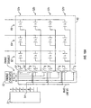
- FIG. 10A is a schematic circuit diagram illustrating an embodiment of an interferometric modulator array having integrated MEMS switches performing a row select function.
- This row select function is useful in some display embodiments when it is desired to drive a display having a high row count with a display driver that has fewer row output lines.
- a display with color pixels may have 3 times as many columns and 4 times as many rows as a black and white display with the same number of pixels.
- each pixel may comprise four red, four blue, and four green modulators.
- the reflective states of the set of 12 "sub-pixels" determine the perceived color of the pixel as a whole. For this embodiment, four times as many row driver outputs would normally be necessary.
- FIG. 10A which illustrates one such set of 12 sub-pixels
- This embodiment may use MEMS switches of the same embodiment as shown in Figures 8A, 8B and 9 , however other MEMS switch embodiments are possible.
- the row select function is used in writing data to the interferometric modulator array.
- data corresponding to states desired for a specific sub-row in the interferometric modulator array are driven onto the column lines shared by multiple rows and sub-rows. Subsequently, the specific sub-row for which the data is intended is driven active, thereby causing the interferometric modulators in that sub-row to assume the desired states.
- the principles discussed here could easily be adapted to perform a column select function for this or another embodiment.
- a portion of a modulator array is shown in Figure 10A as display region 45.
- the term display region has been introduced here to specify a certain area of the entire display.
- the display region is a collection of display elements that typically resolve into a portion of the display presenting a coherent set of image information.
- a typical display region would correspond to a single pixel in the resulting image.
- the display region 45 in Figure 10A comprises three columns, 62, 64, and 66, typically one for each color such as red, green and blue, in the case where display region 45 represents a pixel; and one row, comprising 4 sub-rows 52a-d.
- Each sub-row 52a-d comprises an interferometric modulator from each of the three columns, and a pair of MEMS switches.
- Driver device 51 has one output pin per modulator array row, and a row connection is provided between each driver device 51 output pin and a corresponding row in the modulator array. Row 5 is illustrated in Figures 10A and 9B .
- Timing circuit 53 sequentially drives each of the timing lines active for a portion of the time that the driver device 50 drives a row active, thereby selecting an active sub-row one at a time. While a timing signal is active the MEMS switch connected to that timing signal and also connected to the bias line B1 will be open, and the MEMS switch connected to that timing signal and also connected to the row connection will be closed. The signal on the row connection will pass to interferometric modulators of the sub-row 52a-d.
- Interferometric modulators of an individual sub-row 52a-d will be active when: 1) the driver device 51 drives active the row associated with the sub-rows 52a-d, and 2) the timing circuit 53 drives active the timing signal t1-t4 associated with that particular sub-row 52a-d.
- the timing circuit 53 will sequentially drive each of the timing signals tl-t4 active, each for 1/4 of the time that the row 5 signal is active. While the timing circuit 53 is driving timing signal t1 active the MEMS switch s1 will be open and the MEMS switch s2 will be closed. The interferometric modulators of sub-row 52a will be connected to the row connection driven by driver device 50 output row 5. Because output row 5 is active, the interferometric modulators of sub-row 52a will be driven active. The remaining sub-rows will remain connected to the bias line B1.
- Timing circuit 53 will then drive timing signal t2 active, the interferometric modulators of subrow 52b will be connected to the row connection driven by output row 5, and will be driven active. This sequence continues until the sub-rows 52a-d have each been driven active. Then this sequence repeats for rows 6, 7, and so on.
- the timing signals are shared with all other rows in a column, so that switches for the first sub-row of every row toggle when the first sub-row of any row is active, and so on for the second, third, and fourth sub-rows.
- only the driver output pin for the active row is driven active.
- All non-active rows are held to a bias voltage while the active row is driven active. In this manner, elements in all sub-rows of the entire array except the active sub-row see the same bias voltage independent of the status of the timing signals and consequently independent of the positions of the switches within the sub-row. It should be observed that switching of the non-active row-select switches could be avoided with masking circuits in cases where further reductions in low power consumption are desired
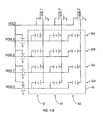
- Figure 10B shows the circuit of Figure 10A with the interferometric modulators of display region 45 and the MEMS switches in physical layout view.
- the columns 62, 64, 66, and the sub-rows 52a-d are indicated.
- the conductive strip 1008, and the terminals 1006 for each of the MEMS switches are shown as seen looking through the moveable material 1014.
- interconnect traces 47 to connect the MEMS switches according to the schematic shown in Figure 10A . Portions of the interconnect routing can be performed underneath the fixed electrodes.
- the traces for the timing lines 49 can be routed beneath those, or even on the bottom of the substrate. Connections can be made with vertical vias.
- the MEMS switches can be fabricated to be the same size as the interferometric modulators. As such, the pitch of the MEMS switches is matched to the pitch of the interferometric modulators. This pitch matching is particularly useful for this embodiment, as well as others which provide signals to each row or to each column. The necessary routing is also conveniently integrated with the interferometric modulators as it can be manufactured using standard metallization interconnect fabrication techniques.
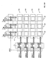
- FIG 11A is a schematic circuit diagram illustrating another embodiment of an interferometric modulator array having integrated MEMS switches.
- the MEMS switches perform a tri-state function.
- This embodiment shows MEMS switches of the same embodiment as that shown in Figure 8A, and 8B , however other MEMS switch embodiments are possible.
- the tri-state function is useful in the interferometric modulator array system for power savings. While the row and column lines are tri-stated the circuitry used to drive those lines can be powered down. With row and column lines tri-stated, the interferometric modulators in the array will hold the values written to them until the charge slowly dissipates, either across the interferometric modulators or through a non-infinite tri-state open resistance. Because the interferometric modulators can be charged in a small fraction of the time it takes for the charge to dissipate, the driving circuitry can be powered down during a significant fraction of the total display operation time.
- a portion of a modulator array is shown in Figure 11A as display region 40, comprising three columns, 42, 44, and 46, typically one for each color such as red, green and blue, in the case where display region 40 represents a pixel; and one row, comprising 4 sub-rows 52a-d.
- Each column comprises a column tri-state MEMS switch, and one interferometric modulator from each sub-row.
- Each sub-row 52a-d comprises an interferometric modulator from each of the three columns, and a sub-row tri-state MEMS switch.
- Each of the column and sub-row tri-state MEMS switches is connected to a signal, HOLD.
- the state of the HOLD signal will determine whether or not the column and sub-row lines are tri-stated or whether the columns and sub-rows are driven.
- Figure 11B shows the circuit of figure 11A with the interferometric modulators of display region 40 and the MEMS switches in physical layout view.
- Figure 11B is similar to Figure 9B , and the significant features discussed with regard to Figure 9B are apparent in Figure 10B as well. As is the case with Figure 9B , the ease of integration is also seen by Figure 10B .
- MEMS switches may be used in any application that utilizes switches, whether or not the application also utilizes interferometric modulators.
- an entire substrate, such as glass may be fabricated with MEMS switches for used in various applications.
- these MEMS switches may be used in a manner analogous to transistors. Accordingly, MEMS switches may replace transistors in any application, logic circuits, or controller and driver devices, for example.
- Figure 12 shows examples of logic functions using a MEMS switch. Because the MEMS switch is a 4 terminal device with no intrinsic polarity these logic functions may be implemented with only two switches.
- the inverter, AND, and OR gates of Figure 12 each use two MEMS switches with their movable layer connected to the movable layer of the other MEMS switch, forming a first input, and one terminal connected to one terminal of the other MEMS switch, forming an output.
- a first switch has both its electrode and other terminal connected to supply
- a second switch has both its electrode and other terminal connected to ground.
- a first switch has its electrode connected to ground and other terminal connected to a second input, and a second switch has its electrode connected to power and its other terminal connected to ground.
- a first switch has its electrode connected to ground and other terminal connected to power, and a second switch has its electrode connected to power and its other terminal connected to a second input.
- single type MEMS switches can be used to create digital logic functions, such as AND, NAND, NOR, OR, XOR, XNOR, and AOI. Other digital logic functions and combinations are also possible.
- MEMS switches may be arranged together to provide logical functions typically found in external components, thereby saving system cost.
- MEMS switches may be arranged for use in the capacity of low leakage transistors, shift registers, or decoders.
- MEMS switches may be used in conjunction with row drivers or column drivers, for example.
- MEMS switches may be manufactured on various substrates, such as glass substrates or plastic substrates, for example. The ability to place switches on large area glass substrates is generally less expensive than silicon substrates, providing an advantage over many forms of conventional transistor based logic.
Landscapes
- Engineering & Computer Science (AREA)
- Physics & Mathematics (AREA)
- Computer Hardware Design (AREA)
- General Physics & Mathematics (AREA)
- Theoretical Computer Science (AREA)
- Nonlinear Science (AREA)
- Optics & Photonics (AREA)
- Microelectronics & Electronic Packaging (AREA)
- Mechanical Light Control Or Optical Switches (AREA)
- Micromachines (AREA)
- Devices For Indicating Variable Information By Combining Individual Elements (AREA)
- Control Of Indicators Other Than Cathode Ray Tubes (AREA)
Abstract
Description
- The field of the invention relates to microelectromechanical systems (MEMS).
- Microelectromechanical systems (MEMS) include micro mechanical elements, actuators, and electronics. Micromechanical elements may be created using deposition, etching, and or other micromachining processes that etch away parts of substrates and/or deposited material layers or that add layers to form electrical and electromechanical devices. One type of MEMS device is called an interferometric modulator. As used herein, the term interferometric modulator or interferometric light modulator refers to a device that selectively absorbs and/or reflects light using the principles of optical interference. In certain embodiments, an interferometric modulator may comprise a pair of conductive plates, one or both of which may be transparent and/or reflective in whole or part and capable of relative motion upon application of an appropriate electrical signal. In a particular embodiment, one plate may comprise a stationary layer deposited on a substrate and the other plate may comprise a metallic membrane separated from the stationary layer by an air gap. As described herein in more detail, the position of one plate in relation to another can change the optical interference of light incident on the interferometric modulator. Such devices have a wide range of applications, and it would be beneficial in the art to utilize and/or modify the characteristics of these types of devices so that their features can be exploited in improving existing products and creating new products that have not yet been developed.
- The US patents
US 2002 / 000 959 A1 andUS 2003 / 043 157 A1 disclose displays comprising a matrix of MEMS interferometric modulators of the collapsible cavity type, wherein each MEMS interferometric modulator comprises a deformable layer that is pulled toward a transparent substrate if a control voltage is applied. The documents furthermore disclose MEMS cantilever switches that are formed on the same substrate as the MEMS interferometric modulators and act as scan and data driver circuits. The claims have been characterized overUS 2002 / 000 959 A1 . - The
Japanese patent JP 2004 - 205 973 A - The
US patents US 2002 / 179 421 A1 andUS 2004 / 0051 929 A1 disclose MEMS switches of the collapsible cavity type, wherein an electrical signal on one electrical terminal is transmitted to another electrical terminal by ohmic or capacitive coupling only if a deformable layer is pulled toward the substrate in response to a control voltage being applied to the switch. - The present invention relates to a display device, a method of displaying an image on a display device and a method of making a MEMS display device as defined in the claims.
-
-
Figure 1 is an isometric view depicting a portion of one embodiment of an interferometric modulator display in which a movable reflective layer of a first interferometric modulator is in a released position and a movable reflective layer of a second interferometric modulator is in an actuated position. -
Figure 2 is a system block diagram illustrating one embodiment of an electronic device incorporating a 3x3 interferometric modulator display. -
Figure 3 is a diagram of movable mirror position versus applied voltage for one exemplary embodiment of an interferometric modulator ofFigure 1 . -
Figure 4 is an illustration of a set of row and column voltages that may be used to drive an interferometric modulator display. -
Figure 5A illustrates one exemplary frame of display data in the 3x3 interferometric modulator display ofFigure 2 . -
Figure 5B illustrates one exemplary timing diagram for row and column signals that may be used to write the frame ofFigure 5A . -
Figure 6A is a system block diagram illustrating an embodiment of a display device. -
Figure 6B is a system block diagram illustrating an embodiment of a display device. -
Figure 7A is a cross section of the device ofFigure 1 . -
Figure 7B is a cross section of an alternative embodiment of an interferometric modulator. -
Figure 7C is a cross section of another alternative embodiment of an interferometric modulator. -
Figure 8A and 8B show an embodiment of a MEMS switch -
Figure 9 shows an embodiment of a MEMS switch -
Figure 10A and10B show a circuit illustrating an embodiment of an interferometric modulator array using MEMS switches -
Figure 11A and11B show a circuit illustrating an embodiment of an interferometric modulator array using MEMS switches -
Figure 12 is an example of an Inverter, AND, and OR logic functions using one type of MEMS switch. - The following detailed description is directed to certain specific embodiments of the invention. However, the invention can be embodied in a multitude of different ways. In this description, reference is made to the drawings wherein like parts are designated with like numerals throughout. As will be apparent from the following description, the embodiments may be implemented in any device that is configured to display an image, whether in motion (e.g., video) or stationary (e.g., still image), and whether textual or pictorial. More particularly, it is contemplated that the embodiments may be implemented in or associated with a variety of electronic devices such as, but not limited to, mobile telephones, wireless devices, personal data assistants (PDAs), hand-held or portable computers, GPS receivers/navigators, cameras, MP3 players, camcorders, game consoles, wrist watches, clocks, calculators, television monitors, flat panel displays, computer monitors, auto displays (e.g., odometer display, etc.), cockpit controls and/or displays, display of camera views (e.g., display of a rear view camera in a vehicle), electronic photographs, electronic billboards or signs, projectors, architectural structures, packaging, and aesthetic structures (e.g., display of images on a piece of jewelry). MEMS devices of similar structure to those described herein can also be used in non-display applications such as in electronic switching devices.
- One interferometric modulator display embodiment comprising an interferometric MEMS display element is illustrated in
Figure 1 . In these devices, the pixels are in either a bright or dark state. In the bright ("on" or "open") state, the display element reflects a large portion of incident visible light to a user. When in the dark ("off" or "closed") state, the display element reflects little incident visible light to the user. Depending on the embodiment, the light reflectance properties of the "on" and "off" states may be reversed. MEMS pixels can be configured to reflect predominantly at selected colors, allowing for a color display in addition to black and white. -
Figure 1 is an isometric view depicting two adjacent pixels in a series of pixels of a visual display, wherein each pixel comprises a MEMS interferometric modulator. In some embodiments, an interferometric modulator display comprises a row/column array of these interferometric modulators. Each interferometric modulator includes a pair of reflective layers positioned at a variable and controllable distance from each other to form a resonant optical cavity with at least one variable dimension. In one embodiment, one of the reflective layers may be moved between two positions. In the first position, referred to herein as the relaxed, the movable layer is positioned at a relatively large distance from a fixed partially reflective layer. In the second position, the movable layer is positioned more closely adjacent to the partially reflective layer. Incident light that reflects from the two layers interferes constructively or destructively depending on the position of the movable reflective layer, producing either an overall reflective or non-reflective state for each pixel. - The depicted portion of the pixel array in
Figure 1 includes two adjacentinterferometric modulators interferometric modulator 12a on the left, a movable and highlyreflective layer 14a is illustrated in a relaxed position at a predetermined distance from a fixed partiallyreflective layer 16a. In theinterferometric modulator 12b on the right, the movable highlyreflective layer 14b is illustrated in an actuated position adjacent to the fixed partiallyreflective layer 16b. - The
fixed layers transparent substrate 20. The layers are patterned into parallel strips, and may form row electrodes in a display device as described further below. Themovable layers row electrodes posts 18 and an intervening sacrificial material deposited between theposts 18. When the sacrificial material is etched away, thedeformable metal layers gap 19. A highly conductive and reflective material such as aluminum may be used for the deformable layers, and these strips may form column electrodes in a display device. - With no applied voltage, the
cavity 19 remains between thelayers pixel 12a inFigure 1 . However, when a potential difference is applied to a selected row and column, the capacitor formed at the intersection of the row and column electrodes at the corresponding pixel becomes charged, and electrostatic forces pull the electrodes together. If the voltage is high enough, the movable layer is deformed and is forced against the fixed layer (a dielectric material which is not illustrated in this Figure may be deposited on the fixed layer to prevent shorting and control the separation distance) as illustrated by thepixel 12b on the right inFigure 1 . The behavior is the same regardless of the polarity of the applied potential difference. In this way, row/column actuation that can control the reflective vs. non-reflective pixel states is analogous in many ways to that used in conventional LCD and other display technologies. -
Figures 2 through 5B illustrate one exemplary process and system for using an array of interferometric modulators in a display application. -
Figure 2 is a system block diagram illustrating one embodiment of an electronic device that may incorporate aspects of the invention. In the exemplary embodiment, the electronic device includes aprocessor 21 which may be any general purpose single- or multi-chip microprocessor such as an ARM, Pentium® , Pentium II® , Pentium III® , Pentium IV® , Pentium® Pro, an 8051, a MIPS® , a Power PC® , an ALPHA® , or any special purpose microprocessor such as a digital signal processor, microcontroller, or a programmable gate array. As is conventional in the art, theprocessor 21 may be configured to execute one or more software modules. In addition to executing an operating system, the processor may be configured to execute one or more software applications, including a web browser, a telephone application, an email program, or any other software application. - In one embodiment, the
processor 21 is also configured to communicate with anarray controller 22. In one embodiment, thearray controller 22 includes arow driver circuit 24 and acolumn driver circuit 26 that provide signals to a display array orpanel 30. The cross section of the array illustrated inFigure 1 is shown by the lines 1-1 inFigure 2 . For MEMS interferometric modulators, the row/column actuation protocol may take advantage of a hysteresis property of these devices illustrated inFigure 3 . It may require, for example, a 10 volt potential difference to cause a movable layer to deform from the relaxed state to the actuated state. However, when the voltage is reduced from that value, the movable layer maintains its state as the voltage drops back below 10 volts. In the exemplary embodiment ofFigure 3 , the movable layer does not relax completely until the voltage drops below 2 volts. There is thus a range of voltage, about 3 to 7 V in the example illustrated inFigure 3 , where there exists a window of applied voltage within which the device is stable in either the relaxed or actuated state. This is referred to herein as the "hysteresis window" or "stability window." For a display array having the hysteresis characteristics ofFigure 3 , the row/column actuation protocol can be designed such that during row strobing, pixels in the strobed row that are to be actuated are exposed to a voltage difference of about 10 volts, and pixels that are to be relaxed are exposed to a voltage difference of close to zero volts. After the strobe, the pixels are exposed to a steady state voltage difference of about 5 volts such that they remain in whatever state the row strobe put them in. After being written, each pixel sees a potential difference within the "stability window" of 3-7 volts in this example. This feature makes the pixel design illustrated inFigure 1 stable under the same applied voltage conditions in either an actuated or relaxed pre-existing state. Since each pixel of the interferometric modulator, whether in the actuated or relaxed state, is essentially a capacitor formed by the fixed and moving reflective layers, this stable state can be held at a voltage within the hysteresis window with almost no power dissipation. Essentially no current flows into the pixel if the applied potential is fixed. - In typical applications, a display frame may be created by asserting the set of column electrodes in accordance with the desired set of actuated pixels in the first row. A row pulse is then applied to the
row 1 electrode, actuating the pixels corresponding to the asserted column lines. The asserted set of column electrodes is then changed to correspond to the desired set of actuated pixels in the second row. A pulse is then applied to therow 2 electrode, actuating the appropriate pixels inrow 2 in accordance with the asserted column electrodes. Therow 1 pixels are unaffected by therow 2 pulse, and remain in the state they were set to during therow 1 pulse. This may be repeated for the entire series of rows in a sequential fashion to produce the frame. Generally, the frames are refreshed and/or updated with new display data by continually repeating this process at some desired number of frames per second. A wide variety of protocols for driving row and column electrodes of pixel arrays to produce display frames are also well known and may be used in conjunction with the present invention. -
Figures 4 ,5A and 5B illustrate one possible actuation protocol for creating a display frame on the 3x3 array ofFigure 2 .Figure 4 illustrates a possible set of column and row voltage levels that may be used for pixels exhibiting the hysteresis curves ofFigure 3 . In theFigure 4 embodiment, actuating a pixel involves setting the appropriate column to ―Vbias, and the appropriate row to +ΔV, which may correspond to -5 volts and +5 volts respectively Relaxing the pixel is accomplished by setting the appropriate column to +Vbias, and the appropriate row to the same +ΔV, producing a zero volt potential difference across the pixel. In those rows where the row voltage is held at zero volts, the pixels are stable in whatever state they were originally in, regardless of whether the column is at +Vbias, or -Vbias. As is also illustrated inFigure 4 , it will be appreciated that voltages of opposite polarity than those described above can be used, e.g., actuating a pixel can involve setting the appropriate column to +Vbias, and the appropriate row to ― ΔV. In this embodiment, releasing the pixel is accomplished by setting the appropriate column to -Ybias, and the appropriate row to the same -ΔV, producing a zero volt potential difference across the pixel. -
Figure 5B is a timing diagram showing a series of row and column signals applied to the 3x3 array ofFigure 2 which will result in the display arrangement illustrated inFigure 5A , where actuated pixels are non-reflective. Prior to writing the frame illustrated inFigure 5A , the pixels can be in any state, and in this example, all the rows are at 0 volts, and all the columns are at +5 volts. With these applied voltages, all pixels are stable in their existing actuated or relaxed states. - In the
Figure 5A frame, pixels (1,1), (1,2), (2,2), (3,2) and (3,3) are actuated. To accomplish this, during a "line time" forrow 1,columns column 3 is set to +5 volts. This does not change the state of any pixels, because all the pixels remain in the 3-7 volt stability window.Row 1 is then strobed with a pulse that goes from 0, up to 5 volts, and back to zero. This actuates the (1,1) and (1,2) pixels and relaxes the (1,3) pixel. No other pixels in the array are affected. To setrow 2 as desired,column 2 is set to-5 volts, andcolumns Row 3 is similarly set by settingcolumns column 1 to +5 volts. Therow 3 strobe sets therow 3 pixels as shown inFigure 5A . After writing the frame, the row potentials are zero, and the column potentials can remain at either +5 or -5 volts, and the display is then stable in the arrangement ofFigure 5A . It will be appreciated that the same procedure can be employed for arrays of dozens or hundreds of rows and columns. It will also be appreciated that the timing, sequence, and levels of voltages used to perform row and column actuation can be varied widely within the general principles outlined above, and the above example is exemplary only, and any actuation voltage method can be used with the systems and methods described herein. -
Figures 6A and 6B are system block diagrams illustrating an embodiment of adisplay device 40. Thedisplay device 40 can be, for example, a cellular or mobile telephone. However, the same components ofdisplay device 40 or slight variations thereof are also illustrative of various types of display devices such as televisions and portable media players. - The
display device 40 includes ahousing 41, adisplay 30, anantenna 43, aspeaker 44, aninput device 48, and amicrophone 46. Thehousing 41 is generally formed from any of a variety of manufacturing processes as are well known to those of skill in the art, including injection molding, and vacuum forming. In addition, thehousing 41 may be made from any of a variety of materials, including but not limited to plastic, metal, glass, rubber, and ceramic, or a combination thereof. In one embodiment thehousing 41 includes removable portions (not shown) that may be interchanged with other removable portions of different color, or containing different logos, pictures, or symbols. - The
display 30 ofexemplary display device 40 may be any of a variety of displays, including a bi-stable display, as described herein. In other examples that do not form part of the invention, thedisplay 30 includes a flat-panel display, such as plasma, EL, OLED, STN LCD, or TFT LCD as described above, or a non-flat-panel display, such as a CRT or other tube device, as is well known to those of skill in the art. However, for purposes of describing the present embodiment, thedisplay 30 includes an interferometric modulator display, as described herein. - The components of one embodiment of
exemplary display device 40 are schematically illustrated inFigure 6B . The illustratedexemplary display device 40 includes ahousing 41 and can include additional components at least partially enclosed therein. For example, in one embodiment, theexemplary display device 40 includes anetwork interface 27 that includes anantenna 43 which is coupled to atransceiver 47. Thetransceiver 47 is connected to aprocessor 21, which is connected to conditioning hardware 52. The conditioning hardware 52 may be configured to condition a signal (e.g. filter a signal). The conditioning hardware 52 is connected to aspeaker 44 and amicrophone 46. Theprocessor 21 is also connected to aninput device 48 and adriver controller 29. Thedriver controller 29 is coupled to aframe buffer 28, and to anarray driver 22, which in turn is coupled to adisplay array 30. Apower supply 50 provides power to all components as required by the particularexemplary display device 40 design. - The
network interface 27 includes theantenna 43 and thetransceiver 47 so that theexemplary display device 40 can communicate with one ore more devices over a network. In one embodiment thenetwork interface 27 may also have some processing capabilities to relieve requirements of theprocessor 21. Theantenna 43 is any antenna known to those of skill in the art for transmitting and receiving signals. In one embodiment, the antenna transmits and receives RF signals according to the IEEE 802.11 standard, including IEEE 802.11(a), (b), or (g). In another embodiment, the antenna transmits and receives RF signals according to the BLUETOOTH standard. In the case of a cellular telephone, the antenna is designed to receive CDMA, GSM, AMPS or other known signals that are used to communicate within a wireless cell phone network. Thetransceiver 47 pre-processes the signals received from theantenna 43 so that they may be received by and further manipulated by theprocessor 21. Thetransceiver 47 also processes signals received from theprocessor 21 so that they may be transmitted from theexemplary display device 40 via theantenna 43. - In an alternative embodiment, the
transceiver 47 can be replaced by a receiver. In yet another alternative embodiment,network interface 27 can be replaced by an image source, which can store or generate image data to be sent to theprocessor 21. For example, the image source can be a digital video disc (DVD) or a hard-disc drive that contains image data, or a software module that generates image data. -
Processor 21 generally controls the overall operation of theexemplary display device 40. Theprocessor 21 receives data, such as compressed image data from thenetwork interface 27 or an image source, and processes the data into raw image data or into a format that is readily processed into raw image data. Theprocessor 21 then sends the processed data to thedriver controller 29 or to framebuffer 28 for storage. Raw data typically refers to the information that identifies the image characteristics at each location within an image. For example, such image characteristics can include color, saturation, and gray-scale level. - In one embodiment, the
processor 21 includes a microcontroller, CPU, or logic unit to control operation of theexemplary display device 40.Conditioning hardware 55 generally includes amplifiers and filters for transmitting signals to thespeaker 44, and for receiving signals from themicrophone 46.Conditioning hardware 55 may be discrete components within theexemplary display device 40, or may be incorporated within theprocessor 21 or other components. - The
driver controller 29 takes the raw image data generated by theprocessor 21 either directly from theprocessor 21 or from theframe buffer 28 and reformats the raw image data appropriately for high speed transmission to thearray driver 22. Specifically, thedriver controller 29 reformats the raw image data into a data flow having a raster-like format, such that it has a time order suitable for scanning across thedisplay array 30. Then thedriver controller 29 sends the formatted information to thearray driver 22. Although adriver controller 29, such as a LCD controller, is often associated with thesystem processor 21 as a stand-alone Integrated Circuit (IC), such controllers may be implemented in many ways. They may be embedded in theprocessor 21 as hardware, embedded in theprocessor 21 as software, or fully integrated in hardware with thearray driver 22. - Typically, the
array driver 22 receives the formatted information from thedriver controller 29 and reformats the video data into a parallel set of waveforms that are applied many times per second to the hundreds and sometimes thousands of leads coming from the display's x-y matrix of pixels. - In one embodiment, the
driver controller 29,array driver 22, anddisplay array 30 are appropriate for any of the types of displays described herein. For example, in one embodiment,driver controller 29 is a conventional display controller or a bi-stable display controller (e.g., an interferometric modulator controller). In another embodiment,array driver 22 is a conventional driver or a bi-stable display driver (e.g., an interferometric modulator display). In one embodiment, adriver controller 29 is integrated with thearray driver 22. Such an embodiment is common in highly integrated systems such as cellular phones, watches, and other small area displays. In yet another embodiment,display array 30 is a typical display array or a bi-stable display array (e.g., a display including an array of interferometric modulators). - The
input device 48 allows a user to control the operation of theexemplary display device 40. In one embodiment,input device 48 includes a keypad, such as a QWERTY keyboard or a telephone keypad, a button, a switch, a touch-sensitive screen, a pressure- or heat-sensitive membrane. In one embodiment, themicrophone 46 is an input device for theexemplary display device 40. When themicrophone 46 is used to input data to the device, voice commands may be provided by a user for controlling operations of theexemplary display device 40. -
Power supply 50 can include a variety of energy storage devices as are well known in the art. For example, in one embodiment,power supply 50 is a rechargeable battery, such as a nickelcadmium battery or a lithium ion battery. In another embodiment,power supply 50 is a renewable energy source, a capacitor, or a solar cell, including a plastic solar cell, and solar-cell paint. In another embodiment,power supply 50 is configured to receive power from a wall outlet. - In some implementations control programmability resides, as described above, in a driver controller which can be located in several places in the electronic display system. In some cases control programmability resides in the
array driver 22. Those of skill in the art will recognize that the above-described optimization may be implemented in any number of hardware and/or software components and in various configurations. - The details of the structure of interferometric modulators that operate in accordance with the principles set forth above may vary widely. For example,
Figures 7A-7C illustrate three different embodiments of the moving mirror structure.Figure 7A is a cross section of the embodiment ofFigure 1 , where a strip ofmetal material 14 is deposited on orthogonally extending supports 18. InFigure 7B , the moveablereflective material 14 is attached to supports at the corners only, ontethers 32. InFigure 7C , the moveablereflective material 14 is suspended from adeformable layer 34. This embodiment has benefits because the structural design and materials used for thereflective material 14 can be optimized with respect to the optical properties, and the structural design and materials used for thedeformable layer 34 can be optimized with respect to desired mechanical properties. The production of various types of interferometric devices is described in a variety of published documents, including, for example,U.S. Published Application 2004/0051929 . A wide variety of known techniques may be used to produce the above described structures involving a series of material deposition, patterning, and etching steps. With some modifications the basic structure of an interferometric modulator can be used as a MEMS switch.Figure 8A is a cross-sectional side view of aMEMS switch 700. TheMEMS switch 700 ofFigure 8A has similar collapsible cavity features as the interferometric modulator ofFigure 7A . TheMEMS switch 700 additionally includes twoterminals 706, an insulatinglayer 710, and aconductive strip 708. TheMEMS switch 700 is a structure that provides selective electrical contact between the twoterminals 706. More particularly, theMEMS switch 700 is considered closed when theterminals 706 are in electrical contact and the MEMS switch is considered open when theterminals 706 are not in electrical contact. In a mechanically relaxed state,terminals 706 are not in electrical contact and, thus, theMEMS switch 700 is open. As shown inFigure 8A , theMEMS switch 700 comprises amoveable material 714, aconductive strip 708, and an insulatinglayer 710 between themoveable material 714 and theconductive strip 708. Asubstrate 720 supports anelectrode 702, and an insulatinglayer 704 on theelectrode 702. Twoterminals 706, separated by a distance, are deposited on and/or through the insulatinglayer 704. Theterminals 706 may connect to other circuitry using vias through insulatinglayer 704 and/orelectrode 702. Insulatinglayer 704 andmoveable material 714 are mechanically separated bysupports 718 in order to define acavity 707. As described above with respect to interferometric modulators, themoveable material 714 is deformable, such that themoveable material 714 may be deformed towards thesubstrate 720 when a voltage difference is applied across themoveable material 714 and theelectrode 702. This is analogous to thereflective material 14,substrate 20, andelectrode 16 ofFigure 7A , and to thereflective layers transparent substrate 20, and thereflective layers Figure 1 . Themoveable material 714 may have on it aninsulator 710, which has upon it theconductive strip 708. Theconductive strip 708 is aligned so that when themoveable material 714 is deflected towards thesubstrate 720 by an applied potential as described above, theconductive strip 708 contacts both of theterminals 706, causing theterminals 706 to be in electrical contact and theMEMS switch 700 to be closed. In this embodiment, theconductive strip 708 is electrically isolated from themoveable material 714 byinsulator 710 so that contact between theterminals 706 and themovable material 714 does not disturb the voltage difference applied across themoveable material 714 and theelectrode 702. In some embodiments, where such isolation is not necessary, theconductive strip 708 and theinsulator 710 will not be needed, and the moveable material itself 714 can function as the conductor that bridges the twoterminals 706. When the voltage applied across themoveable material 714 and theelectrode 702 is reduced below a certain level (as is also described above), themoveable material 714 returns to its mechanically relaxed state and theMEMS switch 700 is opened. -
Figure 8B is a top view ofMEMS switch 700. Thesupports 718, theconductive strip 708, and theterminals 706 are shown as seen looking through themoveable material 714.Conductive strip 708 may be significantly smaller than themoveable material 714. This is to ensure that the electromotive force between themoveable material 714 and theelectrode 702 is larger than the electromotive force between theconductive strip 708 and theelectrode 702 because once the strip contacts the electrodes, the potential on the strip may differ from the potential on the moveable material. -
Figure 9 is a cross-sectional side view of aMEMS switch 800 of another embodiment.MEMS switch 800 has similar constructional features as the interferometric modulator ofFigure 7C . It also has MEMS switch functionality and features similar to those ofMEMS switch 700 inFigure 8A . - MEMS switches built from the same basic structure as interferometric modulators ease the integration of logic and switching functions with interferometric modulator arrays. Although not being part of the invention, it is possible that the other types of switches may be integrated, such as switches fabricated in a manner not similar to the fabrication of the interferometric elements, and more conventional electronic switches fabricated using thin silicon films deposited on the glass substrate. However, because fabrication of interferometric modulator based MEMS switches may be performed using many of the same processing steps that are used in fabricating interferometric modulators, these MEMS switches may be inexpensively integrated onto the same substrate as an array of interferometric modulators used, for example, for a display.
- For example, in one embodiment the MEMS switches and interferometric modulators may be fabricated using the same process, although extra steps may be performed on the interferometric modulators and/or the MEMS switches during the manufacturing process. For example, deposition and etching steps to add terminals to the MEMS switches are unnecessary for the fabrication of interferometric modulators. In such an embodiment some common steps would be performed, such as those for forming the electrodes, etc. The MEMS switch terminals would then be formed. After these steps would follow more steps necessary for both the interferometric modulators and the MEMS switches, thus providing a combined interferometric modulator and MEMS switch array. In yet another embodiment, the same process that is used for manufacturing interferometric modulators is used in manufacturing MEMS switches. The interferometric modulators may first be fabricated on a substrate, followed by fabrication of MEMS switches on the substrate. Similarly, MEMS switches may first be fabricated on a substrate, followed by fabrication of interferometric modulators on the substrate. In either case, the manufacturing process does not require significant modification as the MEMS switches comprise many of the same structures as the interferometric modulators.
-
Figure 10A is a schematic circuit diagram illustrating an embodiment of an interferometric modulator array having integrated MEMS switches performing a row select function. This row select function is useful in some display embodiments when it is desired to drive a display having a high row count with a display driver that has fewer row output lines. For example, a display with color pixels may have 3 times as many columns and 4 times as many rows as a black and white display with the same number of pixels. In these color embodiments, each pixel may comprise four red, four blue, and four green modulators. The reflective states of the set of 12 "sub-pixels" determine the perceived color of the pixel as a whole. For this embodiment, four times as many row driver outputs would normally be necessary. However, with the switch configuration illustrated inFigure 10A (which illustrates one such set of 12 sub-pixels), only one row driver output is necessary for each set of 12 sub-pixels. This embodiment may use MEMS switches of the same embodiment as shown inFigures 8A, 8B and 9 , however other MEMS switch embodiments are possible. The row select function is used in writing data to the interferometric modulator array. In one embodiment data corresponding to states desired for a specific sub-row in the interferometric modulator array are driven onto the column lines shared by multiple rows and sub-rows. Subsequently, the specific sub-row for which the data is intended is driven active, thereby causing the interferometric modulators in that sub-row to assume the desired states. The principles discussed here could easily be adapted to perform a column select function for this or another embodiment. - A portion of a modulator array is shown in
Figure 10A asdisplay region 45. The term display region has been introduced here to specify a certain area of the entire display. The display region is a collection of display elements that typically resolve into a portion of the display presenting a coherent set of image information. A typical display region would correspond to a single pixel in the resulting image. Thedisplay region 45 inFigure 10A comprises three columns, 62, 64, and 66, typically one for each color such as red, green and blue, in the case wheredisplay region 45 represents a pixel; and one row, comprising 4sub-rows 52a-d. Each sub-row 52a-d comprises an interferometric modulator from each of the three columns, and a pair of MEMS switches.Driver device 51 has one output pin per modulator array row, and a row connection is provided between eachdriver device 51 output pin and a corresponding row in the modulator array.Row 5 is illustrated inFigures 10A and9B . - The row select outputs of
driver device 51 become active in a sequential pattern starting withrow 1, then proceeding torow 2 and so on, thereby selecting one active row at a time. Timingcircuit 53 sequentially drives each of the timing lines active for a portion of the time that thedriver device 50 drives a row active, thereby selecting an active sub-row one at a time. While a timing signal is active the MEMS switch connected to that timing signal and also connected to the bias line B1 will be open, and the MEMS switch connected to that timing signal and also connected to the row connection will be closed. The signal on the row connection will pass to interferometric modulators of the sub-row 52a-d. Interferometric modulators of an individual sub-row 52a-d will be active when: 1) thedriver device 51 drives active the row associated with the sub-rows 52a-d, and 2) thetiming circuit 53 drives active the timing signal t1-t4 associated with that particular sub-row 52a-d. - For example, in
Figure 10A , while thedriver device 50 drivesoutput row 5 active, thetiming circuit 53 will sequentially drive each of the timing signals tl-t4 active, each for 1/4 of the time that therow 5 signal is active. While thetiming circuit 53 is driving timing signal t1 active the MEMS switch s1 will be open and the MEMS switch s2 will be closed. The interferometric modulators of sub-row 52a will be connected to the row connection driven bydriver device 50output row 5. Becauseoutput row 5 is active, the interferometric modulators of sub-row 52a will be driven active. The remaining sub-rows will remain connected to the bias line B1. Timingcircuit 53 will then drive timing signal t2 active, the interferometric modulators ofsubrow 52b will be connected to the row connection driven byoutput row 5, and will be driven active. This sequence continues until the sub-rows 52a-d have each been driven active. Then this sequence repeats forrows - As shown in
Figure 10A the timing signals are shared with all other rows in a column, so that switches for the first sub-row of every row toggle when the first sub-row of any row is active, and so on for the second, third, and fourth sub-rows. However, only the driver output pin for the active row is driven active. All non-active rows are held to a bias voltage while the active row is driven active. In this manner, elements in all sub-rows of the entire array except the active sub-row see the same bias voltage independent of the status of the timing signals and consequently independent of the positions of the switches within the sub-row. It should be observed that switching of the non-active row-select switches could be avoided with masking circuits in cases where further reductions in low power consumption are desired -
Figure 10B shows the circuit ofFigure 10A with the interferometric modulators ofdisplay region 45 and the MEMS switches in physical layout view. Thecolumns conductive strip 1008, and theterminals 1006 for each of the MEMS switches are shown as seen looking through the moveable material 1014. Also shown are interconnect traces 47 to connect the MEMS switches according to the schematic shown inFigure 10A . Portions of the interconnect routing can be performed underneath the fixed electrodes. The traces for the timing lines 49 can be routed beneath those, or even on the bottom of the substrate. Connections can be made with vertical vias. - The ease of integration is particularly evident in
Figure 10B . Because they have similar physical features, the MEMS switches can be fabricated to be the same size as the interferometric modulators. As such, the pitch of the MEMS switches is matched to the pitch of the interferometric modulators. This pitch matching is particularly useful for this embodiment, as well as others which provide signals to each row or to each column. The necessary routing is also conveniently integrated with the interferometric modulators as it can be manufactured using standard metallization interconnect fabrication techniques. -
Figure 11A is a schematic circuit diagram illustrating another embodiment of an interferometric modulator array having integrated MEMS switches. In this embodiment the MEMS switches perform a tri-state function. This embodiment shows MEMS switches of the same embodiment as that shown inFigure 8A, and 8B , however other MEMS switch embodiments are possible. The tri-state function is useful in the interferometric modulator array system for power savings. While the row and column lines are tri-stated the circuitry used to drive those lines can be powered down. With row and column lines tri-stated, the interferometric modulators in the array will hold the values written to them until the charge slowly dissipates, either across the interferometric modulators or through a non-infinite tri-state open resistance. Because the interferometric modulators can be charged in a small fraction of the time it takes for the charge to dissipate, the driving circuitry can be powered down during a significant fraction of the total display operation time. - A portion of a modulator array is shown in
Figure 11A asdisplay region 40, comprising three columns, 42, 44, and 46, typically one for each color such as red, green and blue, in the case wheredisplay region 40 represents a pixel; and one row, comprising 4sub-rows 52a-d. Each column comprises a column tri-state MEMS switch, and one interferometric modulator from each sub-row. Each sub-row 52a-d comprises an interferometric modulator from each of the three columns, and a sub-row tri-state MEMS switch. - Each of the column and sub-row tri-state MEMS switches is connected to a signal, HOLD. The state of the HOLD signal will determine whether or not the column and sub-row lines are tri-stated or whether the columns and sub-rows are driven.
-
Figure 11B shows the circuit offigure 11A with the interferometric modulators ofdisplay region 40 and the MEMS switches in physical layout view.Figure 11B is similar toFigure 9B , and the significant features discussed with regard toFigure 9B are apparent inFigure 10B as well. As is the case withFigure 9B , the ease of integration is also seen byFigure 10B . - In another example useful for understanding the invention, MEMS switches may be used in any application that utilizes switches, whether or not the application also utilizes interferometric modulators. Thus, an entire substrate, such as glass, may be fabricated with MEMS switches for used in various applications. As described further below, these MEMS switches may be used in a manner analogous to transistors. Accordingly, MEMS switches may replace transistors in any application, logic circuits, or controller and driver devices, for example.
-
Figure 12 shows examples of logic functions using a MEMS switch. Because the MEMS switch is a 4 terminal device with no intrinsic polarity these logic functions may be implemented with only two switches. The inverter, AND, and OR gates ofFigure 12 each use two MEMS switches with their movable layer connected to the movable layer of the other MEMS switch, forming a first input, and one terminal connected to one terminal of the other MEMS switch, forming an output. In the case of the inverter, a first switch has both its electrode and other terminal connected to supply, and a second switch has both its electrode and other terminal connected to ground. In the case of the AND gate, a first switch has its electrode connected to ground and other terminal connected to a second input, and a second switch has its electrode connected to power and its other terminal connected to ground. In the case of the OR gate, a first switch has its electrode connected to ground and other terminal connected to power, and a second switch has its electrode connected to power and its other terminal connected to a second input. In other examples single type MEMS switches can be used to create digital logic functions, such as AND, NAND, NOR, OR, XOR, XNOR, and AOI. Other digital logic functions and combinations are also possible. - Logic blocks comprising MEMS switches may be arranged together to provide logical functions typically found in external components, thereby saving system cost. For example, MEMS switches may be arranged for use in the capacity of low leakage transistors, shift registers, or decoders. In the context of an interferometric modulator display, MEMS switches may be used in conjunction with row drivers or column drivers, for example. Advantageously, MEMS switches may be manufactured on various substrates, such as glass substrates or plastic substrates, for example. The ability to place switches on large area glass substrates is generally less expensive than silicon substrates, providing an advantage over many forms of conventional transistor based logic.
- While the above detailed description has shown, described, and pointed out novel features as applied to various embodiments, it will be understood that various omissions, substitutions, and changes in the form and details of the device or process illustrated may be made by those skilled in the art without departing from the scope of the invention, as defined in the claims.
Claims (12)
- A display device configured to display an image based on data, the device comprising:means for displaying, configured to display at least a portion of the image, the displaying means comprising rows and columns of MEMS elements (12); andmeans for microelectromechanically switching, configured to switch the data to the displaying means, the switching means comprising one or more additional rows or columns of MEMS elements (700) adjacent to the MEMS elements (12) of the displaying means, wherein each MEMS element (700) of the switching means is configured to drive a plurality of MEMS elements (12) of the displaying means in the corresponding row or column;
wherein the structure of each of the MEMS elements (12) of the displaying means comprises:a substrate (20), on which a control electrode (16) is formed;first and second posts (18) on the substrate (20), wherein the control electrode (16) is between the first and second posts (18); anda layer (14) supported by the first and second posts (18), wherein a portion of the layer (14) between the first and second posts (18) of the MEMS element is deformable and configured to move toward the control electrode (16) according to a hysteresis response to a voltage applied between the control electrode (16) and the layer (14) of the MEMS element (12); andcharacterised in that
each of the MEMS elements (700) of the switching means comprises the same aforementioned structure as the MEMS elements (12) of the displaying means and additionally comprises two electrical terminals (706) formed on the substrate (720), wherein the deformable portion of the layer (14) of the MEMS element is adapted to selectively connect or disconnect the two electrical terminals (706) according to a hysteresis response to the voltage applied between the control electrode (702) and the layer (714) of the MEMS element (700). - The device of Claim 1, further comprising:means for selecting rows or columns, configured to select rows and columns of the MEMS elements (12) of the displaying means; andmeans for switching, configured to switch the data to the selected rows and columns of the MEMS elements (12) of the displaying means.
- The device of Claim 2, wherein the selecting means comprises a controller.
- The device of Claim 1, additionally comprisinga processor (21) that is in electrical communication with said displaying means, said processor being configured to process image data; anda memory device in electrical communication with said processor (21).
- The device of Claim 4, further comprising a driver circuit configured to send at least one signal to said displaying means.
- The device of Claim 5, further comprising a controller configured to send at least a portion of said image data to said driver circuit.
- The device of Claim 4, further comprising an image source module configured to send said image data to said processor (21).
- The device of Claim 7, wherein said image source module comprises at least one of a receiver, transceiver, and transmitter.
- The device of Claim 4, further comprising an input device configured to receive input data and to communicate said input data to said processor (21).
- A method of displaying an image on a display device according to claim 1, wherein the means for micromechanically switching comprise at least one additional row of MEMS elements (700) and at least one additional column of MEMS elements (700) adjacent to the MEMS elements (12) of the displaying means, the method comprising:providing image data for display on the rows and columns of the MEMS
the method characterised by:applying a voltage difference between the control electrode (702) and the layer (714) of at least one of the MEMS elements (700) of the additional columns to switch row data for a row of the MEMS displaying means;applying a voltage difference between the control electrode (702) and the layer (714) of at least one of the MEMS elements (700) of the additional rows to switch column data for a column of the MEMS displaying means; andapplying the switched column data to a column of the MEMS displaying means, and applying the switched row data to a row of the MEMS displaying means. - A method of making a MEMS display device according to claim 1, the method comprising:forming rows and columns of MEMS elements (12) of the displaying means on a substrate; the method characterised byforming one or more rows or columns of MEMS elements (700) of the means for microelectromechanically switching on the same substrate.
- The method of Claim 11, wherein the common substrate (20, 720) used for said MEMS elements (12) of the displaying means and said MEMS elements (700) of the means for microelectromechanically switching is a glass substrate.
Applications Claiming Priority (2)
| Application Number | Priority Date | Filing Date | Title |
|---|---|---|---|
| US61350104P | 2004-09-27 | 2004-09-27 | |
| US11/150,407 US7345805B2 (en) | 2004-09-27 | 2005-06-10 | Interferometric modulator array with integrated MEMS electrical switches |
Publications (3)
| Publication Number | Publication Date |
|---|---|
| EP1640960A2 EP1640960A2 (en) | 2006-03-29 |
| EP1640960A3 EP1640960A3 (en) | 2006-07-26 |
| EP1640960B1 true EP1640960B1 (en) | 2009-11-18 |
Family
ID=35448366
Family Applications (1)
| Application Number | Title | Priority Date | Filing Date |
|---|---|---|---|
| EP05255699A Not-in-force EP1640960B1 (en) | 2004-09-27 | 2005-09-14 | Matrix display with interferometric modulators and integrated MEMS switches |
Country Status (14)
| Country | Link |
|---|---|
| US (4) | US7345805B2 (en) |
| EP (1) | EP1640960B1 (en) |
| JP (2) | JP4652927B2 (en) |
| KR (4) | KR101198081B1 (en) |
| AT (1) | ATE449398T1 (en) |
| AU (1) | AU2005203378A1 (en) |
| BR (1) | BRPI0503935A (en) |
| CA (1) | CA2517038A1 (en) |
| DE (1) | DE602005017724D1 (en) |
| MX (1) | MXPA05009403A (en) |
| MY (1) | MY142573A (en) |
| RU (1) | RU2005129913A (en) |
| SG (2) | SG121059A1 (en) |
| TW (1) | TW200634704A (en) |
Cited By (1)
| Publication number | Priority date | Publication date | Assignee | Title |
|---|---|---|---|---|
| US7777715B2 (en) | 2006-06-29 | 2010-08-17 | Qualcomm Mems Technologies, Inc. | Passive circuits for de-multiplexing display inputs |
Families Citing this family (61)
| Publication number | Priority date | Publication date | Assignee | Title |
|---|---|---|---|---|
| WO1999052006A2 (en) | 1998-04-08 | 1999-10-14 | Etalon, Inc. | Interferometric modulation of radiation |
| US8928967B2 (en) | 1998-04-08 | 2015-01-06 | Qualcomm Mems Technologies, Inc. | Method and device for modulating light |
| WO2003007049A1 (en) * | 1999-10-05 | 2003-01-23 | Iridigm Display Corporation | Photonic mems and structures |
| US6774426B2 (en) * | 2000-12-19 | 2004-08-10 | Micron Technology, Inc. | Flash cell with trench source-line connection |
| TWI289708B (en) | 2002-12-25 | 2007-11-11 | Qualcomm Mems Technologies Inc | Optical interference type color display |
| US7161728B2 (en) * | 2003-12-09 | 2007-01-09 | Idc, Llc | Area array modulation and lead reduction in interferometric modulators |
| US7342705B2 (en) | 2004-02-03 | 2008-03-11 | Idc, Llc | Spatial light modulator with integrated optical compensation structure |
| US7889163B2 (en) | 2004-08-27 | 2011-02-15 | Qualcomm Mems Technologies, Inc. | Drive method for MEMS devices |
| US7499208B2 (en) * | 2004-08-27 | 2009-03-03 | Udc, Llc | Current mode display driver circuit realization feature |
| US7551159B2 (en) * | 2004-08-27 | 2009-06-23 | Idc, Llc | System and method of sensing actuation and release voltages of an interferometric modulator |
| US7675669B2 (en) * | 2004-09-27 | 2010-03-09 | Qualcomm Mems Technologies, Inc. | Method and system for driving interferometric modulators |
| US7345805B2 (en) | 2004-09-27 | 2008-03-18 | Idc, Llc | Interferometric modulator array with integrated MEMS electrical switches |
| US7136213B2 (en) | 2004-09-27 | 2006-11-14 | Idc, Llc | Interferometric modulators having charge persistence |
| US7310179B2 (en) * | 2004-09-27 | 2007-12-18 | Idc, Llc | Method and device for selective adjustment of hysteresis window |
| US7843410B2 (en) | 2004-09-27 | 2010-11-30 | Qualcomm Mems Technologies, Inc. | Method and device for electrically programmable display |
| US8878825B2 (en) | 2004-09-27 | 2014-11-04 | Qualcomm Mems Technologies, Inc. | System and method for providing a variable refresh rate of an interferometric modulator display |
| US7679627B2 (en) * | 2004-09-27 | 2010-03-16 | Qualcomm Mems Technologies, Inc. | Controller and driver features for bi-stable display |
| US7724993B2 (en) | 2004-09-27 | 2010-05-25 | Qualcomm Mems Technologies, Inc. | MEMS switches with deforming membranes |
| US7532195B2 (en) | 2004-09-27 | 2009-05-12 | Idc, Llc | Method and system for reducing power consumption in a display |
| US8310441B2 (en) * | 2004-09-27 | 2012-11-13 | Qualcomm Mems Technologies, Inc. | Method and system for writing data to MEMS display elements |
| US9229222B2 (en) | 2005-02-23 | 2016-01-05 | Pixtronix, Inc. | Alignment methods in fluid-filled MEMS displays |
| US8519945B2 (en) | 2006-01-06 | 2013-08-27 | Pixtronix, Inc. | Circuits for controlling display apparatus |
| US9158106B2 (en) | 2005-02-23 | 2015-10-13 | Pixtronix, Inc. | Display methods and apparatus |
| US7999994B2 (en) | 2005-02-23 | 2011-08-16 | Pixtronix, Inc. | Display apparatus and methods for manufacture thereof |
| US9261694B2 (en) | 2005-02-23 | 2016-02-16 | Pixtronix, Inc. | Display apparatus and methods for manufacture thereof |
| US20070205969A1 (en) | 2005-02-23 | 2007-09-06 | Pixtronix, Incorporated | Direct-view MEMS display devices and methods for generating images thereon |
| US8310442B2 (en) | 2005-02-23 | 2012-11-13 | Pixtronix, Inc. | Circuits for controlling display apparatus |
| US7920136B2 (en) * | 2005-05-05 | 2011-04-05 | Qualcomm Mems Technologies, Inc. | System and method of driving a MEMS display device |
| US7948457B2 (en) | 2005-05-05 | 2011-05-24 | Qualcomm Mems Technologies, Inc. | Systems and methods of actuating MEMS display elements |
| CA2607807A1 (en) * | 2005-05-05 | 2006-11-16 | Qualcomm Incorporated | Dynamic driver ic and display panel configuration |
| US20070126673A1 (en) * | 2005-12-07 | 2007-06-07 | Kostadin Djordjev | Method and system for writing data to MEMS display elements |
| US8391630B2 (en) | 2005-12-22 | 2013-03-05 | Qualcomm Mems Technologies, Inc. | System and method for power reduction when decompressing video streams for interferometric modulator displays |
| US7427201B2 (en) | 2006-01-12 | 2008-09-23 | Green Cloak Llc | Resonant frequency filtered arrays for discrete addressing of a matrix |
| US7916980B2 (en) | 2006-01-13 | 2011-03-29 | Qualcomm Mems Technologies, Inc. | Interconnect structure for MEMS device |
| US8194056B2 (en) | 2006-02-09 | 2012-06-05 | Qualcomm Mems Technologies Inc. | Method and system for writing data to MEMS display elements |
| US8526096B2 (en) | 2006-02-23 | 2013-09-03 | Pixtronix, Inc. | Mechanical light modulators with stressed beams |
| US8049713B2 (en) | 2006-04-24 | 2011-11-01 | Qualcomm Mems Technologies, Inc. | Power consumption optimized display update |
| ATE556272T1 (en) | 2006-10-06 | 2012-05-15 | Qualcomm Mems Technologies Inc | OPTICAL LOSS STRUCTURE IN A LIGHTING DEVICE |
| US8872085B2 (en) | 2006-10-06 | 2014-10-28 | Qualcomm Mems Technologies, Inc. | Display device having front illuminator with turning features |
| US7684106B2 (en) | 2006-11-02 | 2010-03-23 | Qualcomm Mems Technologies, Inc. | Compatible MEMS switch architecture |
| US7724417B2 (en) * | 2006-12-19 | 2010-05-25 | Qualcomm Mems Technologies, Inc. | MEMS switches with deforming membranes |
| US7556981B2 (en) | 2006-12-29 | 2009-07-07 | Qualcomm Mems Technologies, Inc. | Switches for shorting during MEMS etch release |
| US9176318B2 (en) | 2007-05-18 | 2015-11-03 | Pixtronix, Inc. | Methods for manufacturing fluid-filled MEMS displays |
| WO2008097867A1 (en) * | 2007-02-07 | 2008-08-14 | Green Cloak Llc | Displays including addressable trace structures |
| US20080192029A1 (en) * | 2007-02-08 | 2008-08-14 | Michael Hugh Anderson | Passive circuits for de-multiplexing display inputs |
| US8022896B2 (en) * | 2007-08-08 | 2011-09-20 | Qualcomm Mems Technologies, Inc. | ESD protection for MEMS display panels |
| US8068710B2 (en) * | 2007-12-07 | 2011-11-29 | Qualcomm Mems Technologies, Inc. | Decoupled holographic film and diffuser |
| US7977931B2 (en) * | 2008-03-18 | 2011-07-12 | Qualcomm Mems Technologies, Inc. | Family of current/power-efficient high voltage linear regulator circuit architectures |
| US7782522B2 (en) * | 2008-07-17 | 2010-08-24 | Qualcomm Mems Technologies, Inc. | Encapsulation methods for interferometric modulator and MEMS devices |
| US8169679B2 (en) | 2008-10-27 | 2012-05-01 | Pixtronix, Inc. | MEMS anchors |
| US8736590B2 (en) | 2009-03-27 | 2014-05-27 | Qualcomm Mems Technologies, Inc. | Low voltage driver scheme for interferometric modulators |
| JP5310529B2 (en) * | 2009-12-22 | 2013-10-09 | 株式会社豊田中央研究所 | Oscillator for plate member |
| CN103038568A (en) | 2010-04-16 | 2013-04-10 | 弗莱克斯照明第二有限责任公司 | Front illumination device comprising a film-based lightguide |
| EP2558775B1 (en) | 2010-04-16 | 2019-11-13 | FLEx Lighting II, LLC | Illumination device comprising a film-based lightguide |
| US20120153970A1 (en) * | 2010-12-21 | 2012-06-21 | Qualcomm Mems Technologies, Inc. | Capacitive touch sensing devices and methods of manufacturing thereof |
| US9235047B2 (en) | 2011-06-01 | 2016-01-12 | Pixtronix, Inc. | MEMS display pixel control circuits and methods |
| US8836681B2 (en) * | 2011-10-21 | 2014-09-16 | Qualcomm Mems Technologies, Inc. | Method and device for reducing effect of polarity inversion in driving display |
| US9127992B2 (en) * | 2013-03-06 | 2015-09-08 | Ricoh Company, Ltd. | Wide-area pressure sensor with reduced power consumption |
| US9134552B2 (en) | 2013-03-13 | 2015-09-15 | Pixtronix, Inc. | Display apparatus with narrow gap electrostatic actuators |
| US9135867B2 (en) | 2013-04-01 | 2015-09-15 | Pixtronix, Inc. | Display element pixel circuit with voltage equalization |
| JPWO2018051946A1 (en) * | 2016-09-16 | 2019-07-04 | 日本電気株式会社 | Integrated circuit |
Citations (1)
| Publication number | Priority date | Publication date | Assignee | Title |
|---|---|---|---|---|
| JP2004205973A (en) * | 2002-12-26 | 2004-07-22 | Fuji Photo Film Co Ltd | Flat plane display element and method of driving the same |
Family Cites Families (189)
| Publication number | Priority date | Publication date | Assignee | Title |
|---|---|---|---|---|
| US3982239A (en) | 1973-02-07 | 1976-09-21 | North Hills Electronics, Inc. | Saturation drive arrangements for optically bistable displays |
| NL8001281A (en) | 1980-03-04 | 1981-10-01 | Philips Nv | DISPLAY DEVICE. |
| US4441791A (en) | 1980-09-02 | 1984-04-10 | Texas Instruments Incorporated | Deformable mirror light modulator |
| NL8103377A (en) | 1981-07-16 | 1983-02-16 | Philips Nv | DISPLAY DEVICE. |
| US4571603A (en) | 1981-11-03 | 1986-02-18 | Texas Instruments Incorporated | Deformable mirror electrostatic printer |
| NL8200354A (en) | 1982-02-01 | 1983-09-01 | Philips Nv | PASSIVE DISPLAY. |
| US4500171A (en) | 1982-06-02 | 1985-02-19 | Texas Instruments Incorporated | Process for plastic LCD fill hole sealing |
| US4482213A (en) | 1982-11-23 | 1984-11-13 | Texas Instruments Incorporated | Perimeter seal reinforcement holes for plastic LCDs |
| GB8309275D0 (en) * | 1983-04-06 | 1983-05-11 | Allied Colloids Ltd | Dissolution of water soluble polymers in water |
| US4710732A (en) | 1984-07-31 | 1987-12-01 | Texas Instruments Incorporated | Spatial light modulator and method |
| US4566935A (en) | 1984-07-31 | 1986-01-28 | Texas Instruments Incorporated | Spatial light modulator and method |
| US4709995A (en) | 1984-08-18 | 1987-12-01 | Canon Kabushiki Kaisha | Ferroelectric display panel and driving method therefor to achieve gray scale |
| US4596992A (en) | 1984-08-31 | 1986-06-24 | Texas Instruments Incorporated | Linear spatial light modulator and printer |
| US5061049A (en) | 1984-08-31 | 1991-10-29 | Texas Instruments Incorporated | Spatial light modulator and method |
| US5096279A (en) | 1984-08-31 | 1992-03-17 | Texas Instruments Incorporated | Spatial light modulator and method |
| US4662746A (en) | 1985-10-30 | 1987-05-05 | Texas Instruments Incorporated | Spatial light modulator and method |
| US4615595A (en) | 1984-10-10 | 1986-10-07 | Texas Instruments Incorporated | Frame addressed spatial light modulator |
| US5172262A (en) | 1985-10-30 | 1992-12-15 | Texas Instruments Incorporated | Spatial light modulator and method |
| US4859060A (en) | 1985-11-26 | 1989-08-22 | 501 Sharp Kabushiki Kaisha | Variable interferometric device and a process for the production of the same |
| FR2605444A1 (en) | 1986-10-17 | 1988-04-22 | Thomson Csf | METHOD FOR CONTROLLING AN ELECTROOPTIC MATRIX SCREEN AND CONTROL CIRCUIT USING THE SAME |
| US4956619A (en) | 1988-02-19 | 1990-09-11 | Texas Instruments Incorporated | Spatial light modulator |
| US4856863A (en) | 1988-06-22 | 1989-08-15 | Texas Instruments Incorporated | Optical fiber interconnection network including spatial light modulator |
| US5028939A (en) | 1988-08-23 | 1991-07-02 | Texas Instruments Incorporated | Spatial light modulator system |
| US4982184A (en) | 1989-01-03 | 1991-01-01 | General Electric Company | Electrocrystallochromic display and element |
| US5446479A (en) | 1989-02-27 | 1995-08-29 | Texas Instruments Incorporated | Multi-dimensional array video processor system |
| US5170156A (en) | 1989-02-27 | 1992-12-08 | Texas Instruments Incorporated | Multi-frequency two dimensional display system |
| US5206629A (en) | 1989-02-27 | 1993-04-27 | Texas Instruments Incorporated | Spatial light modulator and memory for digitized video display |
| US5272473A (en) | 1989-02-27 | 1993-12-21 | Texas Instruments Incorporated | Reduced-speckle display system |
| US5162787A (en) | 1989-02-27 | 1992-11-10 | Texas Instruments Incorporated | Apparatus and method for digitized video system utilizing a moving display surface |
| US5214420A (en) | 1989-02-27 | 1993-05-25 | Texas Instruments Incorporated | Spatial light modulator projection system with random polarity light |
| US5287096A (en) | 1989-02-27 | 1994-02-15 | Texas Instruments Incorporated | Variable luminosity display system |
| KR100202246B1 (en) | 1989-02-27 | 1999-06-15 | 윌리엄 비. 켐플러 | Apparatus and method for digital video system |
| US5079544A (en) | 1989-02-27 | 1992-01-07 | Texas Instruments Incorporated | Standard independent digitized video system |
| US5192946A (en) | 1989-02-27 | 1993-03-09 | Texas Instruments Incorporated | Digitized color video display system |
| US5214419A (en) | 1989-02-27 | 1993-05-25 | Texas Instruments Incorporated | Planarized true three dimensional display |
| US4954789A (en) | 1989-09-28 | 1990-09-04 | Texas Instruments Incorporated | Spatial light modulator |
| US5124834A (en) | 1989-11-16 | 1992-06-23 | General Electric Company | Transferrable, self-supporting pellicle for elastomer light valve displays and method for making the same |
| US5037173A (en) | 1989-11-22 | 1991-08-06 | Texas Instruments Incorporated | Optical interconnection network |
| US5227900A (en) | 1990-03-20 | 1993-07-13 | Canon Kabushiki Kaisha | Method of driving ferroelectric liquid crystal element |
| CH682523A5 (en) | 1990-04-20 | 1993-09-30 | Suisse Electronique Microtech | A modulation matrix addressed light. |
| US5083857A (en) * | 1990-06-29 | 1992-01-28 | Texas Instruments Incorporated | Multi-level deformable mirror device |
| EP0467048B1 (en) | 1990-06-29 | 1995-09-20 | Texas Instruments Incorporated | Field-updated deformable mirror device |
| US5018256A (en) | 1990-06-29 | 1991-05-28 | Texas Instruments Incorporated | Architecture and process for integrating DMD with control circuit substrates |
| US5216537A (en) | 1990-06-29 | 1993-06-01 | Texas Instruments Incorporated | Architecture and process for integrating DMD with control circuit substrates |
| US5099353A (en) | 1990-06-29 | 1992-03-24 | Texas Instruments Incorporated | Architecture and process for integrating DMD with control circuit substrates |
| US5142405A (en) | 1990-06-29 | 1992-08-25 | Texas Instruments Incorporated | Bistable dmd addressing circuit and method |
| US5526688A (en) | 1990-10-12 | 1996-06-18 | Texas Instruments Incorporated | Digital flexure beam accelerometer and method |
| US5192395A (en) | 1990-10-12 | 1993-03-09 | Texas Instruments Incorporated | Method of making a digital flexure beam accelerometer |
| US5602671A (en) * | 1990-11-13 | 1997-02-11 | Texas Instruments Incorporated | Low surface energy passivation layer for micromechanical devices |
| US5331454A (en) | 1990-11-13 | 1994-07-19 | Texas Instruments Incorporated | Low reset voltage process for DMD |
| US5233459A (en) | 1991-03-06 | 1993-08-03 | Massachusetts Institute Of Technology | Electric display device |
| CA2063744C (en) | 1991-04-01 | 2002-10-08 | Paul M. Urbanus | Digital micromirror device architecture and timing for use in a pulse-width modulated display system |
| US5142414A (en) | 1991-04-22 | 1992-08-25 | Koehler Dale R | Electrically actuatable temporal tristimulus-color device |
| US5226099A (en) | 1991-04-26 | 1993-07-06 | Texas Instruments Incorporated | Digital micromirror shutter device |
| US5179274A (en) | 1991-07-12 | 1993-01-12 | Texas Instruments Incorporated | Method for controlling operation of optical systems and devices |
| US5287215A (en) | 1991-07-17 | 1994-02-15 | Optron Systems, Inc. | Membrane light modulation systems |
| US5168406A (en) | 1991-07-31 | 1992-12-01 | Texas Instruments Incorporated | Color deformable mirror device and method for manufacture |
| US5254980A (en) | 1991-09-06 | 1993-10-19 | Texas Instruments Incorporated | DMD display system controller |
| US5563398A (en) | 1991-10-31 | 1996-10-08 | Texas Instruments Incorporated | Spatial light modulator scanning system |
| US5367878A (en) * | 1991-11-08 | 1994-11-29 | University Of Southern California | Transient energy release microdevices and methods |
| JP3171891B2 (en) * | 1991-11-08 | 2001-06-04 | キヤノン株式会社 | Display control device |
| CA2081753C (en) | 1991-11-22 | 2002-08-06 | Jeffrey B. Sampsell | Dmd scanner |
| US5231388A (en) * | 1991-12-17 | 1993-07-27 | Texas Instruments Incorporated | Color display system using spatial light modulators |
| US5233385A (en) | 1991-12-18 | 1993-08-03 | Texas Instruments Incorporated | White light enhanced color field sequential projection |
| US5233456A (en) | 1991-12-20 | 1993-08-03 | Texas Instruments Incorporated | Resonant mirror and method of manufacture |
| US5296950A (en) | 1992-01-31 | 1994-03-22 | Texas Instruments Incorporated | Optical signal free-space conversion board |
| US5231532A (en) | 1992-02-05 | 1993-07-27 | Texas Instruments Incorporated | Switchable resonant filter for optical radiation |
| US5212582A (en) | 1992-03-04 | 1993-05-18 | Texas Instruments Incorporated | Electrostatically controlled beam steering device and method |
| EP0562424B1 (en) | 1992-03-25 | 1997-05-28 | Texas Instruments Incorporated | Embedded optical calibration system |
| US5312513A (en) * | 1992-04-03 | 1994-05-17 | Texas Instruments Incorporated | Methods of forming multiple phase light modulators |
| US5929831A (en) | 1992-05-19 | 1999-07-27 | Canon Kabushiki Kaisha | Display control apparatus and method |
| US5613103A (en) * | 1992-05-19 | 1997-03-18 | Canon Kabushiki Kaisha | Display control system and method for controlling data based on supply of data |
| JPH0651250A (en) * | 1992-05-20 | 1994-02-25 | Texas Instr Inc <Ti> | Monolithic space optical modulator and memory package |
| JPH06214169A (en) * | 1992-06-08 | 1994-08-05 | Texas Instr Inc <Ti> | Controllable optical and periodic surface filter |
| US5818095A (en) * | 1992-08-11 | 1998-10-06 | Texas Instruments Incorporated | High-yield spatial light modulator with light blocking layer |
| US5327286A (en) | 1992-08-31 | 1994-07-05 | Texas Instruments Incorporated | Real time optical correlation system |
| US5325116A (en) | 1992-09-18 | 1994-06-28 | Texas Instruments Incorporated | Device for writing to and reading from optical storage media |
| US5488505A (en) | 1992-10-01 | 1996-01-30 | Engle; Craig D. | Enhanced electrostatic shutter mosaic modulator |
| CN1057614C (en) | 1993-01-11 | 2000-10-18 | 德克萨斯仪器股份有限公司 | Pixel control circuitry for spatial light modulator |
| US6674562B1 (en) * | 1994-05-05 | 2004-01-06 | Iridigm Display Corporation | Interferometric modulation of radiation |
| US5461411A (en) | 1993-03-29 | 1995-10-24 | Texas Instruments Incorporated | Process and architecture for digital micromirror printer |
| US5489952A (en) | 1993-07-14 | 1996-02-06 | Texas Instruments Incorporated | Method and device for multi-format television |
| US5365283A (en) | 1993-07-19 | 1994-11-15 | Texas Instruments Incorporated | Color phase control for projection display using spatial light modulator |
| US5526172A (en) | 1993-07-27 | 1996-06-11 | Texas Instruments Incorporated | Microminiature, monolithic, variable electrical signal processor and apparatus including same |
| US5619061A (en) * | 1993-07-27 | 1997-04-08 | Texas Instruments Incorporated | Micromechanical microwave switching |
| US5581272A (en) | 1993-08-25 | 1996-12-03 | Texas Instruments Incorporated | Signal generator for controlling a spatial light modulator |
| US5552925A (en) | 1993-09-07 | 1996-09-03 | John M. Baker | Electro-micro-mechanical shutters on transparent substrates |
| US5483260A (en) * | 1993-09-10 | 1996-01-09 | Dell Usa, L.P. | Method and apparatus for simplified video monitor control |
| US5457493A (en) | 1993-09-15 | 1995-10-10 | Texas Instruments Incorporated | Digital micro-mirror based image simulation system |
| US5497197A (en) | 1993-11-04 | 1996-03-05 | Texas Instruments Incorporated | System and method for packaging data into video processor |
| US5526051A (en) | 1993-10-27 | 1996-06-11 | Texas Instruments Incorporated | Digital television system |
| US5459602A (en) | 1993-10-29 | 1995-10-17 | Texas Instruments | Micro-mechanical optical shutter |
| US5452024A (en) | 1993-11-01 | 1995-09-19 | Texas Instruments Incorporated | DMD display system |
| US5517347A (en) | 1993-12-01 | 1996-05-14 | Texas Instruments Incorporated | Direct view deformable mirror device |
| US5583688A (en) | 1993-12-21 | 1996-12-10 | Texas Instruments Incorporated | Multi-level digital micromirror device |
| US5598565A (en) * | 1993-12-29 | 1997-01-28 | Intel Corporation | Method and apparatus for screen power saving |
| US5448314A (en) | 1994-01-07 | 1995-09-05 | Texas Instruments | Method and apparatus for sequential color imaging |
| US5444566A (en) | 1994-03-07 | 1995-08-22 | Texas Instruments Incorporated | Optimized electronic operation of digital micromirror devices |
| US20010003487A1 (en) * | 1996-11-05 | 2001-06-14 | Mark W. Miles | Visible spectrum modulator arrays |
| US6680792B2 (en) * | 1994-05-05 | 2004-01-20 | Iridigm Display Corporation | Interferometric modulation of radiation |
| US6710908B2 (en) * | 1994-05-05 | 2004-03-23 | Iridigm Display Corporation | Controlling micro-electro-mechanical cavities |
| US7550794B2 (en) * | 2002-09-20 | 2009-06-23 | Idc, Llc | Micromechanical systems device comprising a displaceable electrode and a charge-trapping layer |
| US7460291B2 (en) * | 1994-05-05 | 2008-12-02 | Idc, Llc | Separable modulator |
| US7123216B1 (en) * | 1994-05-05 | 2006-10-17 | Idc, Llc | Photonic MEMS and structures |
| US6040937A (en) * | 1994-05-05 | 2000-03-21 | Etalon, Inc. | Interferometric modulation |
| US5497172A (en) | 1994-06-13 | 1996-03-05 | Texas Instruments Incorporated | Pulse width modulation for spatial light modulator with split reset addressing |
| US5454906A (en) | 1994-06-21 | 1995-10-03 | Texas Instruments Inc. | Method of providing sacrificial spacer for micro-mechanical devices |
| US5499062A (en) | 1994-06-23 | 1996-03-12 | Texas Instruments Incorporated | Multiplexed memory timing with block reset and secondary memory |
| JPH0822024A (en) * | 1994-07-05 | 1996-01-23 | Mitsubishi Electric Corp | Active matrix substrate and its production |
| US5552924A (en) | 1994-11-14 | 1996-09-03 | Texas Instruments Incorporated | Micromechanical device having an improved beam |
| US5610624A (en) * | 1994-11-30 | 1997-03-11 | Texas Instruments Incorporated | Spatial light modulator with reduced possibility of an on state defect |
| US5612713A (en) * | 1995-01-06 | 1997-03-18 | Texas Instruments Incorporated | Digital micro-mirror device with block data loading |
| US5567334A (en) | 1995-02-27 | 1996-10-22 | Texas Instruments Incorporated | Method for creating a digital micromirror device using an aluminum hard mask |
| US5610438A (en) * | 1995-03-08 | 1997-03-11 | Texas Instruments Incorporated | Micro-mechanical device with non-evaporable getter |
| US5535047A (en) | 1995-04-18 | 1996-07-09 | Texas Instruments Incorporated | Active yoke hidden hinge digital micromirror device |
| US5578976A (en) | 1995-06-22 | 1996-11-26 | Rockwell International Corporation | Micro electromechanical RF switch |
| JP3799092B2 (en) * | 1995-12-29 | 2006-07-19 | アジレント・テクノロジーズ・インク | Light modulation device and display device |
| US7471444B2 (en) * | 1996-12-19 | 2008-12-30 | Idc, Llc | Interferometric modulation of radiation |
| EP0877272B1 (en) * | 1997-05-08 | 2002-07-31 | Texas Instruments Incorporated | Improvements in or relating to spatial light modulators |
| US6750876B1 (en) * | 1997-11-16 | 2004-06-15 | Ess Technology, Inc. | Programmable display controller |
| US6028690A (en) * | 1997-11-26 | 2000-02-22 | Texas Instruments Incorporated | Reduced micromirror mirror gaps for improved contrast ratio |
| US6180428B1 (en) * | 1997-12-12 | 2001-01-30 | Xerox Corporation | Monolithic scanning light emitting devices using micromachining |
| KR100253378B1 (en) * | 1997-12-15 | 2000-04-15 | 김영환 | Apparatus for displaying output data in asic(application specific ic) |
| US6037719A (en) * | 1998-04-09 | 2000-03-14 | Hughes Electronics Corporation | Matrix-addressed display having micromachined electromechanical switches |
| US6323982B1 (en) * | 1998-05-22 | 2001-11-27 | Texas Instruments Incorporated | Yield superstructure for digital micromirror device |
| JP4074714B2 (en) * | 1998-09-25 | 2008-04-09 | 富士フイルム株式会社 | Array type light modulation element and flat display driving method |
| US6323834B1 (en) * | 1998-10-08 | 2001-11-27 | International Business Machines Corporation | Micromechanical displays and fabrication method |
| JP3919954B2 (en) * | 1998-10-16 | 2007-05-30 | 富士フイルム株式会社 | Array type light modulation element and flat display driving method |
| JP2000214804A (en) | 1999-01-20 | 2000-08-04 | Fuji Photo Film Co Ltd | Light modulation element, aligner, and planar display |
| NL1015202C2 (en) * | 1999-05-20 | 2002-03-26 | Nec Corp | Active matrix type liquid crystal display device includes adder provided by making scanning line and pixel electrode connected to gate electrode of TFT to overlap via insulating and semiconductor films |
| TW523727B (en) * | 1999-05-27 | 2003-03-11 | Koninkl Philips Electronics Nv | Display device |
| US6201633B1 (en) * | 1999-06-07 | 2001-03-13 | Xerox Corporation | Micro-electromechanical based bistable color display sheets |
| US6862029B1 (en) * | 1999-07-27 | 2005-03-01 | Hewlett-Packard Development Company, L.P. | Color display system |
| WO2003007049A1 (en) * | 1999-10-05 | 2003-01-23 | Iridigm Display Corporation | Photonic mems and structures |
| US6549338B1 (en) * | 1999-11-12 | 2003-04-15 | Texas Instruments Incorporated | Bandpass filter to reduce thermal impact of dichroic light shift |
| US6552840B2 (en) * | 1999-12-03 | 2003-04-22 | Texas Instruments Incorporated | Electrostatic efficiency of micromechanical devices |
| US6674090B1 (en) * | 1999-12-27 | 2004-01-06 | Xerox Corporation | Structure and method for planar lateral oxidation in active |
| US6545335B1 (en) * | 1999-12-27 | 2003-04-08 | Xerox Corporation | Structure and method for electrical isolation of optoelectronic integrated circuits |
| US6548908B2 (en) * | 1999-12-27 | 2003-04-15 | Xerox Corporation | Structure and method for planar lateral oxidation in passive devices |
| US6466358B2 (en) * | 1999-12-30 | 2002-10-15 | Texas Instruments Incorporated | Analog pulse width modulation cell for digital micromechanical device |
| AU2001272094A1 (en) * | 2000-03-01 | 2001-09-12 | British Telecommunications Public Limited Company | Data transfer method and apparatus |
| JP4357071B2 (en) * | 2000-03-09 | 2009-11-04 | 株式会社東芝 | Semiconductor device and semiconductor memory device |
| JP3538109B2 (en) * | 2000-03-16 | 2004-06-14 | 日本電気株式会社 | Micro machine switch |
| JP4669619B2 (en) | 2000-03-27 | 2011-04-13 | 富士フイルム株式会社 | Laminated polyester film |
| US6356085B1 (en) * | 2000-05-09 | 2002-03-12 | Pacesetter, Inc. | Method and apparatus for converting capacitance to voltage |
| JP3843703B2 (en) * | 2000-06-13 | 2006-11-08 | 富士ゼロックス株式会社 | Optical writable recording and display device |
| US6853129B1 (en) * | 2000-07-28 | 2005-02-08 | Candescent Technologies Corporation | Protected substrate structure for a field emission display device |
| US6859218B1 (en) * | 2000-11-07 | 2005-02-22 | Hewlett-Packard Development Company, L.P. | Electronic display devices and methods |
| US6433917B1 (en) * | 2000-11-22 | 2002-08-13 | Ball Semiconductor, Inc. | Light modulation device and system |
| JP2002221935A (en) * | 2000-11-24 | 2002-08-09 | Mitsubishi Electric Corp | Display device |
| JP2002175053A (en) | 2000-12-07 | 2002-06-21 | Sony Corp | Active matrix display and mobile terminal which uses the same |
| JP4109992B2 (en) * | 2001-01-30 | 2008-07-02 | 株式会社アドバンテスト | Switch and integrated circuit device |
| US6657832B2 (en) * | 2001-04-26 | 2003-12-02 | Texas Instruments Incorporated | Mechanically assisted restoring force support for micromachined membranes |
| US6862022B2 (en) * | 2001-07-20 | 2005-03-01 | Hewlett-Packard Development Company, L.P. | Method and system for automatically selecting a vertical refresh rate for a video display monitor |
| US6870581B2 (en) * | 2001-10-30 | 2005-03-22 | Sharp Laboratories Of America, Inc. | Single panel color video projection display using reflective banded color falling-raster illumination |
| US6574033B1 (en) * | 2002-02-27 | 2003-06-03 | Iridigm Display Corporation | Microelectromechanical systems device and method for fabricating same |
| US7283112B2 (en) * | 2002-03-01 | 2007-10-16 | Microsoft Corporation | Reflective microelectrical mechanical structure (MEMS) optical modulator and optical display system |
| TW544787B (en) * | 2002-09-18 | 2003-08-01 | Promos Technologies Inc | Method of forming self-aligned contact structure with locally etched gate conductive layer |
| US6813060B1 (en) * | 2002-12-09 | 2004-11-02 | Sandia Corporation | Electrical latching of microelectromechanical devices |
| GB0229692D0 (en) * | 2002-12-19 | 2003-01-29 | Koninkl Philips Electronics Nv | Active matrix display device |
| JP2004004553A (en) | 2003-02-10 | 2004-01-08 | Seiko Epson Corp | Liquid crystal display panel and driving circuit |
| US6829132B2 (en) * | 2003-04-30 | 2004-12-07 | Hewlett-Packard Development Company, L.P. | Charge control of micro-electromechanical device |
| US6903860B2 (en) * | 2003-11-01 | 2005-06-07 | Fusao Ishii | Vacuum packaged micromirror arrays and methods of manufacturing the same |
| US7190380B2 (en) * | 2003-09-26 | 2007-03-13 | Hewlett-Packard Development Company, L.P. | Generating and displaying spatially offset sub-frames |
| US7173314B2 (en) * | 2003-08-13 | 2007-02-06 | Hewlett-Packard Development Company, L.P. | Storage device having a probe and a storage cell with moveable parts |
| US20050057442A1 (en) * | 2003-08-28 | 2005-03-17 | Olan Way | Adjacent display of sequential sub-images |
| US20050068583A1 (en) * | 2003-09-30 | 2005-03-31 | Gutkowski Lawrence J. | Organizing a digital image |
| US6861277B1 (en) * | 2003-10-02 | 2005-03-01 | Hewlett-Packard Development Company, L.P. | Method of forming MEMS device |
| US7161728B2 (en) * | 2003-12-09 | 2007-01-09 | Idc, Llc | Area array modulation and lead reduction in interferometric modulators |
| US7532194B2 (en) * | 2004-02-03 | 2009-05-12 | Idc, Llc | Driver voltage adjuster |
| US7329931B2 (en) * | 2004-06-18 | 2008-02-12 | Nantero, Inc. | Receiver circuit using nanotube-based switches and transistors |
| US7560299B2 (en) * | 2004-08-27 | 2009-07-14 | Idc, Llc | Systems and methods of actuating MEMS display elements |
| US7499208B2 (en) * | 2004-08-27 | 2009-03-03 | Udc, Llc | Current mode display driver circuit realization feature |
| US7889163B2 (en) * | 2004-08-27 | 2011-02-15 | Qualcomm Mems Technologies, Inc. | Drive method for MEMS devices |
| US7515147B2 (en) * | 2004-08-27 | 2009-04-07 | Idc, Llc | Staggered column drive circuit systems and methods |
| US7551159B2 (en) * | 2004-08-27 | 2009-06-23 | Idc, Llc | System and method of sensing actuation and release voltages of an interferometric modulator |
| US7602375B2 (en) * | 2004-09-27 | 2009-10-13 | Idc, Llc | Method and system for writing data to MEMS display elements |
| US7724993B2 (en) * | 2004-09-27 | 2010-05-25 | Qualcomm Mems Technologies, Inc. | MEMS switches with deforming membranes |
| US7545550B2 (en) * | 2004-09-27 | 2009-06-09 | Idc, Llc | Systems and methods of actuating MEMS display elements |
| US20060066594A1 (en) * | 2004-09-27 | 2006-03-30 | Karen Tyger | Systems and methods for driving a bi-stable display element |
| US7675669B2 (en) * | 2004-09-27 | 2010-03-09 | Qualcomm Mems Technologies, Inc. | Method and system for driving interferometric modulators |
| US8310441B2 (en) * | 2004-09-27 | 2012-11-13 | Qualcomm Mems Technologies, Inc. | Method and system for writing data to MEMS display elements |
| US7446927B2 (en) * | 2004-09-27 | 2008-11-04 | Idc, Llc | MEMS switch with set and latch electrodes |
| US7532195B2 (en) * | 2004-09-27 | 2009-05-12 | Idc, Llc | Method and system for reducing power consumption in a display |
| US7345805B2 (en) * | 2004-09-27 | 2008-03-18 | Idc, Llc | Interferometric modulator array with integrated MEMS electrical switches |
| EP1800173A1 (en) * | 2004-09-27 | 2007-06-27 | Idc, Llc | Method and device for multistate interferometric light modulation |
| US7136213B2 (en) * | 2004-09-27 | 2006-11-14 | Idc, Llc | Interferometric modulators having charge persistence |
| US7843410B2 (en) * | 2004-09-27 | 2010-11-30 | Qualcomm Mems Technologies, Inc. | Method and device for electrically programmable display |
| US8878825B2 (en) * | 2004-09-27 | 2014-11-04 | Qualcomm Mems Technologies, Inc. | System and method for providing a variable refresh rate of an interferometric modulator display |
-
2005
- 2005-06-10 US US11/150,407 patent/US7345805B2/en not_active Expired - Fee Related
- 2005-07-29 MY MYPI20053521A patent/MY142573A/en unknown
- 2005-08-01 AU AU2005203378A patent/AU2005203378A1/en not_active Abandoned
- 2005-08-11 TW TW094127355A patent/TW200634704A/en unknown
- 2005-08-11 JP JP2005232880A patent/JP4652927B2/en not_active Expired - Fee Related
- 2005-08-15 SG SG200505164A patent/SG121059A1/en unknown
- 2005-08-15 SG SG200906349-6A patent/SG155963A1/en unknown
- 2005-08-25 CA CA002517038A patent/CA2517038A1/en not_active Abandoned
- 2005-09-02 MX MXPA05009403A patent/MXPA05009403A/en active IP Right Grant
- 2005-09-14 EP EP05255699A patent/EP1640960B1/en not_active Not-in-force
- 2005-09-14 AT AT05255699T patent/ATE449398T1/en not_active IP Right Cessation
- 2005-09-14 DE DE602005017724T patent/DE602005017724D1/en active Active
- 2005-09-21 KR KR1020050087709A patent/KR101198081B1/en not_active IP Right Cessation
- 2005-09-23 BR BRPI0503935-5A patent/BRPI0503935A/en not_active IP Right Cessation
- 2005-09-26 RU RU2005129913/28A patent/RU2005129913A/en not_active Application Discontinuation
-
2008
- 2008-03-17 US US12/050,094 patent/US7859739B2/en not_active Expired - Fee Related
-
2009
- 2009-01-05 JP JP2009000342A patent/JP5054040B2/en not_active Expired - Fee Related
-
2010
- 2010-12-06 US US12/961,402 patent/US8223424B2/en not_active Expired - Fee Related
-
2012
- 2012-06-20 KR KR1020120066149A patent/KR101284822B1/en not_active IP Right Cessation
- 2012-06-20 US US13/528,609 patent/US8437071B2/en not_active Expired - Fee Related
- 2012-09-27 KR KR1020120107807A patent/KR101290628B1/en not_active IP Right Cessation
-
2013
- 2013-01-11 KR KR1020130003471A patent/KR20130020816A/en not_active Application Discontinuation
Patent Citations (1)
| Publication number | Priority date | Publication date | Assignee | Title |
|---|---|---|---|---|
| JP2004205973A (en) * | 2002-12-26 | 2004-07-22 | Fuji Photo Film Co Ltd | Flat plane display element and method of driving the same |
Cited By (1)
| Publication number | Priority date | Publication date | Assignee | Title |
|---|---|---|---|---|
| US7777715B2 (en) | 2006-06-29 | 2010-08-17 | Qualcomm Mems Technologies, Inc. | Passive circuits for de-multiplexing display inputs |
Also Published As
| Publication number | Publication date |
|---|---|
| KR20120123235A (en) | 2012-11-08 |
| ATE449398T1 (en) | 2009-12-15 |
| US8437071B2 (en) | 2013-05-07 |
| JP2009163248A (en) | 2009-07-23 |
| KR20130020816A (en) | 2013-02-28 |
| RU2005129913A (en) | 2007-04-10 |
| TW200634704A (en) | 2006-10-01 |
| US20060103613A1 (en) | 2006-05-18 |
| KR20120099351A (en) | 2012-09-10 |
| KR20060051479A (en) | 2006-05-19 |
| US20080158647A1 (en) | 2008-07-03 |
| DE602005017724D1 (en) | 2009-12-31 |
| SG155963A1 (en) | 2009-10-29 |
| US7859739B2 (en) | 2010-12-28 |
| BRPI0503935A (en) | 2006-05-09 |
| EP1640960A2 (en) | 2006-03-29 |
| MXPA05009403A (en) | 2006-03-29 |
| EP1640960A3 (en) | 2006-07-26 |
| KR101284822B1 (en) | 2013-07-10 |
| CA2517038A1 (en) | 2006-03-27 |
| US8223424B2 (en) | 2012-07-17 |
| JP2006099064A (en) | 2006-04-13 |
| KR101290628B1 (en) | 2013-07-29 |
| AU2005203378A1 (en) | 2006-04-13 |
| KR101198081B1 (en) | 2012-11-05 |
| US20110095973A1 (en) | 2011-04-28 |
| MY142573A (en) | 2010-12-15 |
| JP5054040B2 (en) | 2012-10-24 |
| JP4652927B2 (en) | 2011-03-16 |
| SG121059A1 (en) | 2006-04-26 |
| US20120256819A1 (en) | 2012-10-11 |
| US7345805B2 (en) | 2008-03-18 |
Similar Documents
| Publication | Publication Date | Title |
|---|---|---|
| EP1640960B1 (en) | Matrix display with interferometric modulators and integrated MEMS switches | |
| US7724993B2 (en) | MEMS switches with deforming membranes | |
| US7446927B2 (en) | MEMS switch with set and latch electrodes | |
| US7843410B2 (en) | Method and device for electrically programmable display | |
| US7499208B2 (en) | Current mode display driver circuit realization feature | |
| US7349136B2 (en) | Method and device for a display having transparent components integrated therein | |
| US7724417B2 (en) | MEMS switches with deforming membranes | |
| US20080158648A1 (en) | Peripheral switches for MEMS display test | |
| EP1784812A2 (en) | Systems and methods of actuating mems display elements | |
| EP1809568A2 (en) | Mems switches with deforming membranes | |
| EP1949165B1 (en) | MEMS switch with set and latch electrodes |
Legal Events
| Date | Code | Title | Description |
|---|---|---|---|
| PUAI | Public reference made under article 153(3) epc to a published international application that has entered the european phase |
Free format text: ORIGINAL CODE: 0009012 |
|
| AK | Designated contracting states |
Kind code of ref document: A2 Designated state(s): AT BE BG CH CY CZ DE DK EE ES FI FR GB GR HU IE IS IT LI LT LU LV MC NL PL PT RO SE SI SK TR |
|
| AX | Request for extension of the european patent |
Extension state: AL BA HR MK YU |
|
| PUAL | Search report despatched |
Free format text: ORIGINAL CODE: 0009013 |
|
| AK | Designated contracting states |
Kind code of ref document: A3 Designated state(s): AT BE BG CH CY CZ DE DK EE ES FI FR GB GR HU IE IS IT LI LT LU LV MC NL PL PT RO SE SI SK TR |
|
| AX | Request for extension of the european patent |
Extension state: AL BA HR MK YU |
|
| 17P | Request for examination filed |
Effective date: 20070117 |
|
| 17Q | First examination report despatched |
Effective date: 20070215 |
|
| AKX | Designation fees paid |
Designated state(s): AT BE BG CH CY CZ DE DK EE ES FI FR GB GR HU IE IS IT LI LT LU LV MC NL PL PT RO SE SI SK TR |
|
| GRAP | Despatch of communication of intention to grant a patent |
Free format text: ORIGINAL CODE: EPIDOSNIGR1 |
|
| GRAS | Grant fee paid |
Free format text: ORIGINAL CODE: EPIDOSNIGR3 |
|
| GRAA | (expected) grant |
Free format text: ORIGINAL CODE: 0009210 |
|
| AK | Designated contracting states |
Kind code of ref document: B1 Designated state(s): AT BE BG CH CY CZ DE DK EE ES FI FR GB GR HU IE IS IT LI LT LU LV MC NL PL PT RO SE SI SK TR |
|
| REG | Reference to a national code |
Ref country code: GB Ref legal event code: FG4D |
|
| REG | Reference to a national code |
Ref country code: CH Ref legal event code: EP |
|
| RAP2 | Party data changed (patent owner data changed or rights of a patent transferred) |
Owner name: QUALCOMM MEMS TECHNOLOGIES, INC. |
|
| REG | Reference to a national code |
Ref country code: IE Ref legal event code: FG4D |
|
| REF | Corresponds to: |
Ref document number: 602005017724 Country of ref document: DE Date of ref document: 20091231 Kind code of ref document: P |
|
| NLT2 | Nl: modifications (of names), taken from the european patent patent bulletin |
Owner name: QUALCOMM MEMS TECHNOLOGIES, INC. Effective date: 20091202 |
|
| REG | Reference to a national code |
Ref country code: NL Ref legal event code: VDEP Effective date: 20091118 |
|
| LTIE | Lt: invalidation of european patent or patent extension |
Effective date: 20091118 |
|
| PG25 | Lapsed in a contracting state [announced via postgrant information from national office to epo] |
Ref country code: IS Free format text: LAPSE BECAUSE OF FAILURE TO SUBMIT A TRANSLATION OF THE DESCRIPTION OR TO PAY THE FEE WITHIN THE PRESCRIBED TIME-LIMIT Effective date: 20100318 Ref country code: LT Free format text: LAPSE BECAUSE OF FAILURE TO SUBMIT A TRANSLATION OF THE DESCRIPTION OR TO PAY THE FEE WITHIN THE PRESCRIBED TIME-LIMIT Effective date: 20091118 Ref country code: ES Free format text: LAPSE BECAUSE OF FAILURE TO SUBMIT A TRANSLATION OF THE DESCRIPTION OR TO PAY THE FEE WITHIN THE PRESCRIBED TIME-LIMIT Effective date: 20100228 Ref country code: PT Free format text: LAPSE BECAUSE OF FAILURE TO SUBMIT A TRANSLATION OF THE DESCRIPTION OR TO PAY THE FEE WITHIN THE PRESCRIBED TIME-LIMIT Effective date: 20100318 Ref country code: FI Free format text: LAPSE BECAUSE OF FAILURE TO SUBMIT A TRANSLATION OF THE DESCRIPTION OR TO PAY THE FEE WITHIN THE PRESCRIBED TIME-LIMIT Effective date: 20091118 Ref country code: SE Free format text: LAPSE BECAUSE OF FAILURE TO SUBMIT A TRANSLATION OF THE DESCRIPTION OR TO PAY THE FEE WITHIN THE PRESCRIBED TIME-LIMIT Effective date: 20091118 |
|
| PG25 | Lapsed in a contracting state [announced via postgrant information from national office to epo] |
Ref country code: CY Free format text: LAPSE BECAUSE OF FAILURE TO SUBMIT A TRANSLATION OF THE DESCRIPTION OR TO PAY THE FEE WITHIN THE PRESCRIBED TIME-LIMIT Effective date: 20091118 Ref country code: SI Free format text: LAPSE BECAUSE OF FAILURE TO SUBMIT A TRANSLATION OF THE DESCRIPTION OR TO PAY THE FEE WITHIN THE PRESCRIBED TIME-LIMIT Effective date: 20091118 Ref country code: PL Free format text: LAPSE BECAUSE OF FAILURE TO SUBMIT A TRANSLATION OF THE DESCRIPTION OR TO PAY THE FEE WITHIN THE PRESCRIBED TIME-LIMIT Effective date: 20091118 Ref country code: LV Free format text: LAPSE BECAUSE OF FAILURE TO SUBMIT A TRANSLATION OF THE DESCRIPTION OR TO PAY THE FEE WITHIN THE PRESCRIBED TIME-LIMIT Effective date: 20091118 |
|
| PG25 | Lapsed in a contracting state [announced via postgrant information from national office to epo] |
Ref country code: AT Free format text: LAPSE BECAUSE OF FAILURE TO SUBMIT A TRANSLATION OF THE DESCRIPTION OR TO PAY THE FEE WITHIN THE PRESCRIBED TIME-LIMIT Effective date: 20091118 Ref country code: BE Free format text: LAPSE BECAUSE OF FAILURE TO SUBMIT A TRANSLATION OF THE DESCRIPTION OR TO PAY THE FEE WITHIN THE PRESCRIBED TIME-LIMIT Effective date: 20091118 |
|
| PG25 | Lapsed in a contracting state [announced via postgrant information from national office to epo] |
Ref country code: NL Free format text: LAPSE BECAUSE OF FAILURE TO SUBMIT A TRANSLATION OF THE DESCRIPTION OR TO PAY THE FEE WITHIN THE PRESCRIBED TIME-LIMIT Effective date: 20091118 Ref country code: RO Free format text: LAPSE BECAUSE OF FAILURE TO SUBMIT A TRANSLATION OF THE DESCRIPTION OR TO PAY THE FEE WITHIN THE PRESCRIBED TIME-LIMIT Effective date: 20091118 Ref country code: BG Free format text: LAPSE BECAUSE OF FAILURE TO SUBMIT A TRANSLATION OF THE DESCRIPTION OR TO PAY THE FEE WITHIN THE PRESCRIBED TIME-LIMIT Effective date: 20100218 Ref country code: DK Free format text: LAPSE BECAUSE OF FAILURE TO SUBMIT A TRANSLATION OF THE DESCRIPTION OR TO PAY THE FEE WITHIN THE PRESCRIBED TIME-LIMIT Effective date: 20091118 Ref country code: EE Free format text: LAPSE BECAUSE OF FAILURE TO SUBMIT A TRANSLATION OF THE DESCRIPTION OR TO PAY THE FEE WITHIN THE PRESCRIBED TIME-LIMIT Effective date: 20091118 |
|
| PG25 | Lapsed in a contracting state [announced via postgrant information from national office to epo] |
Ref country code: CZ Free format text: LAPSE BECAUSE OF FAILURE TO SUBMIT A TRANSLATION OF THE DESCRIPTION OR TO PAY THE FEE WITHIN THE PRESCRIBED TIME-LIMIT Effective date: 20091118 Ref country code: SK Free format text: LAPSE BECAUSE OF FAILURE TO SUBMIT A TRANSLATION OF THE DESCRIPTION OR TO PAY THE FEE WITHIN THE PRESCRIBED TIME-LIMIT Effective date: 20091118 |
|
| PLBE | No opposition filed within time limit |
Free format text: ORIGINAL CODE: 0009261 |
|
| STAA | Information on the status of an ep patent application or granted ep patent |
Free format text: STATUS: NO OPPOSITION FILED WITHIN TIME LIMIT |
|
| 26N | No opposition filed |
Effective date: 20100819 |
|
| PG25 | Lapsed in a contracting state [announced via postgrant information from national office to epo] |
Ref country code: GR Free format text: LAPSE BECAUSE OF FAILURE TO SUBMIT A TRANSLATION OF THE DESCRIPTION OR TO PAY THE FEE WITHIN THE PRESCRIBED TIME-LIMIT Effective date: 20100219 |
|
| PGFP | Annual fee paid to national office [announced via postgrant information from national office to epo] |
Ref country code: FR Payment date: 20100921 Year of fee payment: 6 |
|
| PG25 | Lapsed in a contracting state [announced via postgrant information from national office to epo] |
Ref country code: IT Free format text: LAPSE BECAUSE OF FAILURE TO SUBMIT A TRANSLATION OF THE DESCRIPTION OR TO PAY THE FEE WITHIN THE PRESCRIBED TIME-LIMIT Effective date: 20091118 |
|
| PG25 | Lapsed in a contracting state [announced via postgrant information from national office to epo] |
Ref country code: MC Free format text: LAPSE BECAUSE OF NON-PAYMENT OF DUE FEES Effective date: 20100930 |
|
| REG | Reference to a national code |
Ref country code: CH Ref legal event code: PL |
|
| PG25 | Lapsed in a contracting state [announced via postgrant information from national office to epo] |
Ref country code: IE Free format text: LAPSE BECAUSE OF NON-PAYMENT OF DUE FEES Effective date: 20100914 Ref country code: LI Free format text: LAPSE BECAUSE OF NON-PAYMENT OF DUE FEES Effective date: 20100930 Ref country code: CH Free format text: LAPSE BECAUSE OF NON-PAYMENT OF DUE FEES Effective date: 20100930 |
|
| REG | Reference to a national code |
Ref country code: FR Ref legal event code: ST Effective date: 20120531 |
|
| PG25 | Lapsed in a contracting state [announced via postgrant information from national office to epo] |
Ref country code: FR Free format text: LAPSE BECAUSE OF NON-PAYMENT OF DUE FEES Effective date: 20110930 |
|
| PG25 | Lapsed in a contracting state [announced via postgrant information from national office to epo] |
Ref country code: LU Free format text: LAPSE BECAUSE OF NON-PAYMENT OF DUE FEES Effective date: 20100914 Ref country code: HU Free format text: LAPSE BECAUSE OF FAILURE TO SUBMIT A TRANSLATION OF THE DESCRIPTION OR TO PAY THE FEE WITHIN THE PRESCRIBED TIME-LIMIT Effective date: 20100519 |
|
| PG25 | Lapsed in a contracting state [announced via postgrant information from national office to epo] |
Ref country code: TR Free format text: LAPSE BECAUSE OF FAILURE TO SUBMIT A TRANSLATION OF THE DESCRIPTION OR TO PAY THE FEE WITHIN THE PRESCRIBED TIME-LIMIT Effective date: 20091118 |
|
| PGFP | Annual fee paid to national office [announced via postgrant information from national office to epo] |
Ref country code: GB Payment date: 20140826 Year of fee payment: 10 |
|
| PGFP | Annual fee paid to national office [announced via postgrant information from national office to epo] |
Ref country code: DE Payment date: 20140930 Year of fee payment: 10 |
|
| REG | Reference to a national code |
Ref country code: DE Ref legal event code: R119 Ref document number: 602005017724 Country of ref document: DE |
|
| GBPC | Gb: european patent ceased through non-payment of renewal fee |
Effective date: 20150914 |
|
| PG25 | Lapsed in a contracting state [announced via postgrant information from national office to epo] |
Ref country code: DE Free format text: LAPSE BECAUSE OF NON-PAYMENT OF DUE FEES Effective date: 20160401 Ref country code: GB Free format text: LAPSE BECAUSE OF NON-PAYMENT OF DUE FEES Effective date: 20150914 |