EP1636036B1 - Ink-jet printhead substrate, driving control method, ink-jet printhead and ink-jet printing apparatus - Google Patents
Ink-jet printhead substrate, driving control method, ink-jet printhead and ink-jet printing apparatus Download PDFInfo
- Publication number
- EP1636036B1 EP1636036B1 EP04735669A EP04735669A EP1636036B1 EP 1636036 B1 EP1636036 B1 EP 1636036B1 EP 04735669 A EP04735669 A EP 04735669A EP 04735669 A EP04735669 A EP 04735669A EP 1636036 B1 EP1636036 B1 EP 1636036B1
- Authority
- EP
- European Patent Office
- Prior art keywords
- ink
- circuit
- jet printhead
- amplitude level
- voltage amplitude
- Prior art date
- Legal status (The legal status is an assumption and is not a legal conclusion. Google has not performed a legal analysis and makes no representation as to the accuracy of the status listed.)
- Expired - Lifetime
Links
- 239000000758 substrate Substances 0.000 title claims abstract description 62
- 238000007641 inkjet printing Methods 0.000 title claims description 9
- 238000000034 method Methods 0.000 title claims description 7
- 239000004065 semiconductor Substances 0.000 claims description 11
- 238000007599 discharging Methods 0.000 claims description 9
- 238000006243 chemical reaction Methods 0.000 claims description 7
- 239000000976 ink Substances 0.000 description 47
- 238000010586 diagram Methods 0.000 description 18
- 238000007639 printing Methods 0.000 description 13
- 239000003086 colorant Substances 0.000 description 6
- 230000004044 response Effects 0.000 description 4
- 238000004140 cleaning Methods 0.000 description 3
- 238000005516 engineering process Methods 0.000 description 3
- 238000011084 recovery Methods 0.000 description 3
- 230000005540 biological transmission Effects 0.000 description 2
- 238000004519 manufacturing process Methods 0.000 description 2
- 239000011159 matrix material Substances 0.000 description 2
- 238000012545 processing Methods 0.000 description 2
- XUIMIQQOPSSXEZ-UHFFFAOYSA-N Silicon Chemical compound [Si] XUIMIQQOPSSXEZ-UHFFFAOYSA-N 0.000 description 1
- 230000015572 biosynthetic process Effects 0.000 description 1
- 230000003139 buffering effect Effects 0.000 description 1
- 238000010276 construction Methods 0.000 description 1
- 230000007423 decrease Effects 0.000 description 1
- 238000011161 development Methods 0.000 description 1
- 230000018109 developmental process Effects 0.000 description 1
- 230000000694 effects Effects 0.000 description 1
- 238000010438 heat treatment Methods 0.000 description 1
- 238000012544 monitoring process Methods 0.000 description 1
- 229910052710 silicon Inorganic materials 0.000 description 1
- 239000010703 silicon Substances 0.000 description 1
- 238000012546 transfer Methods 0.000 description 1
Images


Classifications
-
- B—PERFORMING OPERATIONS; TRANSPORTING
- B41—PRINTING; LINING MACHINES; TYPEWRITERS; STAMPS
- B41J—TYPEWRITERS; SELECTIVE PRINTING MECHANISMS, i.e. MECHANISMS PRINTING OTHERWISE THAN FROM A FORME; CORRECTION OF TYPOGRAPHICAL ERRORS
- B41J2/00—Typewriters or selective printing mechanisms characterised by the printing or marking process for which they are designed
- B41J2/005—Typewriters or selective printing mechanisms characterised by the printing or marking process for which they are designed characterised by bringing liquid or particles selectively into contact with a printing material
- B41J2/01—Ink jet
- B41J2/015—Ink jet characterised by the jet generation process
- B41J2/04—Ink jet characterised by the jet generation process generating single droplets or particles on demand
- B41J2/045—Ink jet characterised by the jet generation process generating single droplets or particles on demand by pressure, e.g. electromechanical transducers
- B41J2/05—Ink jet characterised by the jet generation process generating single droplets or particles on demand by pressure, e.g. electromechanical transducers produced by the application of heat
-
- B—PERFORMING OPERATIONS; TRANSPORTING
- B41—PRINTING; LINING MACHINES; TYPEWRITERS; STAMPS
- B41J—TYPEWRITERS; SELECTIVE PRINTING MECHANISMS, i.e. MECHANISMS PRINTING OTHERWISE THAN FROM A FORME; CORRECTION OF TYPOGRAPHICAL ERRORS
- B41J2/00—Typewriters or selective printing mechanisms characterised by the printing or marking process for which they are designed
- B41J2/005—Typewriters or selective printing mechanisms characterised by the printing or marking process for which they are designed characterised by bringing liquid or particles selectively into contact with a printing material
- B41J2/01—Ink jet
- B41J2/015—Ink jet characterised by the jet generation process
- B41J2/04—Ink jet characterised by the jet generation process generating single droplets or particles on demand
- B41J2/045—Ink jet characterised by the jet generation process generating single droplets or particles on demand by pressure, e.g. electromechanical transducers
- B41J2/04501—Control methods or devices therefor, e.g. driver circuits, control circuits
- B41J2/04541—Specific driving circuit
-
- B—PERFORMING OPERATIONS; TRANSPORTING
- B41—PRINTING; LINING MACHINES; TYPEWRITERS; STAMPS
- B41J—TYPEWRITERS; SELECTIVE PRINTING MECHANISMS, i.e. MECHANISMS PRINTING OTHERWISE THAN FROM A FORME; CORRECTION OF TYPOGRAPHICAL ERRORS
- B41J2/00—Typewriters or selective printing mechanisms characterised by the printing or marking process for which they are designed
- B41J2/005—Typewriters or selective printing mechanisms characterised by the printing or marking process for which they are designed characterised by bringing liquid or particles selectively into contact with a printing material
- B41J2/01—Ink jet
- B41J2/015—Ink jet characterised by the jet generation process
- B41J2/04—Ink jet characterised by the jet generation process generating single droplets or particles on demand
- B41J2/045—Ink jet characterised by the jet generation process generating single droplets or particles on demand by pressure, e.g. electromechanical transducers
- B41J2/04501—Control methods or devices therefor, e.g. driver circuits, control circuits
- B41J2/04543—Block driving
-
- B—PERFORMING OPERATIONS; TRANSPORTING
- B41—PRINTING; LINING MACHINES; TYPEWRITERS; STAMPS
- B41J—TYPEWRITERS; SELECTIVE PRINTING MECHANISMS, i.e. MECHANISMS PRINTING OTHERWISE THAN FROM A FORME; CORRECTION OF TYPOGRAPHICAL ERRORS
- B41J2/00—Typewriters or selective printing mechanisms characterised by the printing or marking process for which they are designed
- B41J2/005—Typewriters or selective printing mechanisms characterised by the printing or marking process for which they are designed characterised by bringing liquid or particles selectively into contact with a printing material
- B41J2/01—Ink jet
- B41J2/015—Ink jet characterised by the jet generation process
- B41J2/04—Ink jet characterised by the jet generation process generating single droplets or particles on demand
- B41J2/045—Ink jet characterised by the jet generation process generating single droplets or particles on demand by pressure, e.g. electromechanical transducers
- B41J2/04501—Control methods or devices therefor, e.g. driver circuits, control circuits
- B41J2/04546—Multiplexing
-
- B—PERFORMING OPERATIONS; TRANSPORTING
- B41—PRINTING; LINING MACHINES; TYPEWRITERS; STAMPS
- B41J—TYPEWRITERS; SELECTIVE PRINTING MECHANISMS, i.e. MECHANISMS PRINTING OTHERWISE THAN FROM A FORME; CORRECTION OF TYPOGRAPHICAL ERRORS
- B41J2/00—Typewriters or selective printing mechanisms characterised by the printing or marking process for which they are designed
- B41J2/005—Typewriters or selective printing mechanisms characterised by the printing or marking process for which they are designed characterised by bringing liquid or particles selectively into contact with a printing material
- B41J2/01—Ink jet
- B41J2/015—Ink jet characterised by the jet generation process
- B41J2/04—Ink jet characterised by the jet generation process generating single droplets or particles on demand
- B41J2/045—Ink jet characterised by the jet generation process generating single droplets or particles on demand by pressure, e.g. electromechanical transducers
- B41J2/04501—Control methods or devices therefor, e.g. driver circuits, control circuits
- B41J2/04548—Details of power line section of control circuit
-
- B—PERFORMING OPERATIONS; TRANSPORTING
- B41—PRINTING; LINING MACHINES; TYPEWRITERS; STAMPS
- B41J—TYPEWRITERS; SELECTIVE PRINTING MECHANISMS, i.e. MECHANISMS PRINTING OTHERWISE THAN FROM A FORME; CORRECTION OF TYPOGRAPHICAL ERRORS
- B41J2/00—Typewriters or selective printing mechanisms characterised by the printing or marking process for which they are designed
- B41J2/005—Typewriters or selective printing mechanisms characterised by the printing or marking process for which they are designed characterised by bringing liquid or particles selectively into contact with a printing material
- B41J2/01—Ink jet
- B41J2/015—Ink jet characterised by the jet generation process
- B41J2/04—Ink jet characterised by the jet generation process generating single droplets or particles on demand
- B41J2/045—Ink jet characterised by the jet generation process generating single droplets or particles on demand by pressure, e.g. electromechanical transducers
- B41J2/04501—Control methods or devices therefor, e.g. driver circuits, control circuits
- B41J2/0455—Details of switching sections of circuit, e.g. transistors
-
- B—PERFORMING OPERATIONS; TRANSPORTING
- B41—PRINTING; LINING MACHINES; TYPEWRITERS; STAMPS
- B41J—TYPEWRITERS; SELECTIVE PRINTING MECHANISMS, i.e. MECHANISMS PRINTING OTHERWISE THAN FROM A FORME; CORRECTION OF TYPOGRAPHICAL ERRORS
- B41J2/00—Typewriters or selective printing mechanisms characterised by the printing or marking process for which they are designed
- B41J2/005—Typewriters or selective printing mechanisms characterised by the printing or marking process for which they are designed characterised by bringing liquid or particles selectively into contact with a printing material
- B41J2/01—Ink jet
- B41J2/015—Ink jet characterised by the jet generation process
- B41J2/04—Ink jet characterised by the jet generation process generating single droplets or particles on demand
- B41J2/045—Ink jet characterised by the jet generation process generating single droplets or particles on demand by pressure, e.g. electromechanical transducers
- B41J2/04501—Control methods or devices therefor, e.g. driver circuits, control circuits
- B41J2/0458—Control methods or devices therefor, e.g. driver circuits, control circuits controlling heads based on heating elements forming bubbles
Definitions
- This invention relates an ink-jet printhead substrate, an ink-jet printhead and a printing apparatus that uses this printhead. More particularly, the invention relates to an ink-jet printhead in which electrothermal transducers for generating thermal energy necessary to discharge ink and driving circuits for driving the transducers are formed on the same substrate, and to a printing apparatus that uses this printhead.
- an electrothermal transducer (heater) of a printhead mounted on a printing apparatus in accordance with an ink-jet scheme and the driving circuit of the transducer are formed on the same substrate using semiconductor process technology as illustrated in, e.g., USP 6,290,334 and US 6,435,668 .
- a digital circuit, etc., for sensing the state of the semiconductor substrate, e.g., the substrate temperature is formed on the same substrate in addition to the driving circuit, an ink supply port is located at the center of the substrate and a heater is disposed at a position opposing the port.
- Fig. 5 is a diagram schematically illustrating a semiconductor substrate for an ink-jet printhead of this type, i.e., a semiconductor substrate for an ink-jet printhead that includes a circuit for outputting a digital signal indicative of sensed temperature.
- reference numeral 500 denotes a substrate obtained by integrally forming heaters and driving circuits by semiconductor process technology, 501 a heater/driver array having a structure in which a plurality of heaters and driver circuits are arrayed, and 502 an ink supply port for supplying ink from the reverse side of the substrate.
- reference numeral 503 denotes a shift register for temporarily holding print data to be printed.
- Reference numeral 507 denotes a decoder circuit that outputs a heater-block selection signal for driving the heaters in the heater/driver array 501 on a per-heater-block basis.
- Reference numeral 504 denotes an input circuit that includes a buffer circuit for inputting a digital signal to the shift register 503 and decoder 507.
- Reference numeral 510 denotes an input terminal that includes a terminal for supplying logic-element voltage VDD, a terminal CLK for inputting a clock and a terminal for inputting print data, etc.
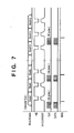
- Fig. 7 is a timing chart for describing a series of operations up to sending of print information to the shift register 503 and supplying of current to heaters to drive the same.
- Print data is supplied to DATA_A and DATA_B terminals in sync with a clock pulse applied to the CLK terminal.
- the shift register 503 stores the supplied print data temporarily and a latch circuit latches the print data in response to a latch signal applied to a BG terminal.
- a block signal which is for selecting a group of heaters that have been partitioned into a desired block, and the print data that has been latched by the latch signal are subsequently subjected to an AND operation in matrix form, and the heater current flows in sync with an HE signal that directly decides current drive time. This series of operations is repeated block by block to perform printing.
- Fig. 6A is one segment's worth of an equivalent circuit for driving current into a heater for discharging ink. Further, Fig. 6B is an equivalent circuit that corresponds to one bit of a shift register and latch circuit for temporarily storing image data to be printed.
- a block select signal that is input to an AND gate 601 is a signal sent from the decoder 507 for selecting heater groups partitioned into blocks. Further, a bit signal that enters the AND gate 601 is a signal transferred to the shift register 503 and thenceforth latched by a latch signal. In order to turn on each segment selectively by print data, the AND gate 601 obtains the AND, in matrix form, between the block select signal and bit signal.
- Reference numeral 605 denotes a VH power-supply line that serves as a power supply for heater drive, 606 a heater and 607 a driver transistor for passing current into the heater 606.
- Reference numeral 602 denotes an inverter circuit for receiving and buffering the output of the AND gate 601.
- Reference numeral 603 denotes a VDD power-supply line that serves as a power supply for the inverter circuit 602.
- Reference numeral 608 denotes an inverter circuit serving as a buffer for receiving the buffered output of the inverter circuit 602.
- Reference numeral 604 denotes a VHT power-supply line serving as a power supply, which is supplied to a buffer 608, for supplying the gate voltage of the driver transistor.
- the inverter 602 and shift register 503, etc. are digital circuits and they basically operate in accordance with low/high pulses.
- applied pulses for interfacing print information of the printhead per se and for driving the heaters also are digital signals, and an exchange of signals with the outside is performed in its entirety by low/high logic pulses.
- the amplitudes of these logic pulses are 0V/5V or 0V/3.3V, and the power supply VDD of the digital circuits is supplied with a signal one of these voltages. Accordingly, pulses having the amplitude of the VDD voltage are input to the AND gate 601 and are input to the inverter circuit 608 of the next stage through a buffer constituted by the two-stage inverter circuit 602.
- the ON resistance of the driver transistor 607 is large, a voltage drop ascribable to heater current that flows through this portion increases and it becomes necessary to apply an excessively high voltage to the heaters. The result is wasteful power consumption.
- the voltage applied to the gate of this transistor is required to be set high. In the circuit illustrated in Fig. 6A , therefore, it becomes necessary to provide a circuit for making a conversion to pulses having a voltage amplitude higher than the voltage VDD.
- the power-supply line 604 of voltage VHT higher than voltage VDD is provided and a segment selection signal that has entered in response to the pulse having the amplitude of the voltage VDD is converted to a pulse having the amplitude of voltage VHT by a buffer circuit that includes the inverter circuit 608. After the conversion is thus made to the pulse having the amplitude of voltage VHT, the pulse is applied to the gate of the driver transistor 607.
- an arrangement is adopted in which the exchange of signals with the outside and signal processing by the internal digital circuit are performed in their entirety by pulses having the voltage amplitude (voltage for driving the logic circuits) of VDD, and each segment is provided with a circuit (pulse-amplitude converting circuit) for effecting a conversion to pulses of the VHT voltage amplitude (the voltage for element drive) immediately before the gate of driver transistor 607 is driven.
- a printhead takes on a form in which a plurality of individual segments are arrayed at a high density, and therefore in a case where the segments are arrayed at a density of, e.g., 600 dpi, segment width in the array direction is limited to about 42.3 ⁇ m. If it is attempted to fit the entirety of the circuit of the kind shown in Fig. 6A in this pitch for driving each of the elements, then the length of each segment will increase in a direction perpendicular to the array direction.
- Fig. 10 is a circuit diagram of an equivalent circuit in a case where the pulse-amplitude converting circuit in Fig. 6A is shown in detail. It will be understood from observing this diagram that the pulse-amplitude converting circuit, particularly a level converter indicated by the dashed lines, is composed of a number of transistors, and therefore a greater chip area becomes necessary.
- the pulse-amplitude converting circuit provided for each segment leads to an increase in the length of each segment, invites an increase in chip size and raises cost. More specifically, with the above-described layout, the chip becomes larger in a direction perpendicular to the segment array and the increase in chip size becomes pronounced. Further, in a case where the pulse-amplitude converting circuit is provided for every segment, e.g., in a case where consideration is given to a printhead having, e.g., 256 segments, the number of buffer circuits required necessitates at least 256 inverters. This invites a decline in yield and in a more complicated circuit structure and is a cause of higher cost.
- the present invention has been devised in view of the foregoing problems and its object is to provide a circuit arrangement in which a voltage for driving logic is converted to a voltage for driving elements without increasing the length of segments in a direction perpendicular to the array direction of the segments.
- Another object of the present invention is to reduce pulse-amplitude converting circuits and reduce the number of elements formed on the substrate, thereby raising yield and simplifying circuit structure.
- print used in the present invention signifies not only imparting an image having the meaning of text or graphics to a printing medium but also imparting an image that does not have the meaning of a pattern or the like.
- substrate not only refers to a simple substrate comprising a silicon semiconductor but also to a substrate that has been provided with various elements, circuits and wiring.
- the substrate made have the shape of a board or chip.
- on the substrate not only refers simply to the top of the substrate but also to the surface of the substrate and the interior of the substrate in the vicinity of the surface.
- built-in used in the present invention refers not only to the simple placing of separate elements on the substrate but also to the formation and manufacture of elements on the substrate as an integral part thereof by a semiconductor-circuit manufacturing process or the like.
- a segment selection signal that has been input in response to a pulse having the amplitude of a VDD voltage can be converted to a pulse having the amplitude of VHT voltage without increasing the length of each segment in a direction perpendicular to the array direction of the segments.
- conversion of pulse width is performed before the AND is taken between the output signal from the decoder side and the signal from the side of the shift register, and therefore a pulse-amplitude converting circuit provided for every segment is no longer necessary.
- the number of pulse-amplitude converting circuits themselves can be reduced to the sum of the number of time-division drive blocks (the number of signal outputs from the decoder) and the number of data items corresponding to each block (the number of outputs from the shift register), yield is raised and the circuit arrangement is simplified.
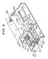
- Fig. 8 is an external view of an ink-jet printing apparatus to which the present invention is applicable.
- a lead screw 5005 rotates via driving force transmission gears 5011, 5009 in operative association with the forward and reverse rotation of a driver motor 5013.
- a carriage HC has a pin (not shown) that mates with a helical groove 5005 of the lead screw 5004 and that is moved back and forth in directions of arrows a and b as the lead screw 5004 rotates.
- An ink-jet cartridge IJC is mounted on the carriage- HC.
- Reference numeral 5002 denotes a paper retaining plate which presses paper against a platen 5000 along the traveling direction of the carriage.
- Reference numerals 5007, 5008 denote photosensors which constitute home position sensing means for verifying the presence of a carriage lever 5006 in the vicinity of the photosensors and changing over the direction in which the motor 5013 is rotated.
- Reference numeral 5016 denotes a member which supports a cap member 5022, which is for capping the front side of the printhead.
- Reference numeral 5015 denotes suction means for applying suction to the cap. The suction means subjects the cap to suction recovery via an opening 5023 inside the cap.
- Reference numeral denotes a cleaning blade
- reference numeral 5019 denotes a member which makes it possible to move the blade back and forth. These are supported on a support plate 5018 of the main body. It goes without saying that the blade need not be of this form and that a well-known cleaning blade can be applied to this example.
- Reference numeral 5021 denotes a lever for starting the suction of the suction recovery operation. The lever moves with movement of a cam 5020 engaged with the carriage. Movement is controlled by well-known transmission means whereby the driving force from the driver motor is changed over as by a clutch.
- reference numeral 1700 denotes an interface, 1701 an MPU, 1702 a program ROM for storing a control program executed by the MPU 1701, and 1703 a dynamic-type RAM (DRAM below) for storing various data (such as the above-mentioned print signal as well as print data supplied to the head) in advance.
- Reference numeral 1704 denotes a gate array for controlling supply of print data to the printhead 1708. A signal for driving the printhead is supplied via this gate array. Further, the gate array controls transfer of data between the interface 1700, MPU 1701 and RAM 1703.
- Reference 1710 denotes a carrier motor for transporting the printhead 1708, and 1709 a transport motor 1709 for transporting printing paper.
- Reference numeral 1704 denotes an ink-jet printhead substrate mounted on the printhead 1708 and including an ink-discharge heater and its drive circuit.
- Reference numerals 1706, 1707 denote motor drivers for driving the transport motor 1709 and carrier motor 1710, respectively.
- the print signal When a print signal enters the interface 1700, the print signal is converted to print data for printing between the gate array 1704 and MPU 1701.
- the motor drivers 1706, 1707 are driven and the ink discharge heaters are driven to perform printing in accordance with the print data sent to the printhead substrate within the printhead 1708.
- Fig. 11 is a perspective view showing a detailed outer appearance of the configuration of an inkjet cartridge IJC.
- the inkjet cartridge IJC is comprised of a cartridge IJCK that discharges black ink and a cartridge IJCC that discharges three colors of ink, cyan (C), magenta (M) and yellow (Y). These two cartridges are mutually separable, with each being independently detachably mounted on the carriage HC.
- the cartridge IJCK is comprised of an ink tank ITK that contains black ink and a printhead IJHK that prints by discharging black ink, combined in an integrated structure.
- the cartridge IJCC is comprised of an ink tank ITC that contains ink of three colors, cyan (C), magenta (M) and yellow (Y), and a printhead IJHC that prints by discharging ink of these colors, combined in an integrated structure.
- an array of nozzles that discharges black ink, an array of nozzles that discharges cyan ink, an array of nozzles that discharges magenta ink and an array of nozzles that discharges yellow ink are aligned in a direction of movement of the carriage, the arrayed direction of the nozzles being disposed perpendicular to the carriage movement direction.
- Fig. 12 is a perspective view showing a three-dimensional structure of a printhead IJHC that discharges three colors of ink.
- Fig. 12 shows the flow of ink supplied from the ink tank ITK.
- the printhead IJHC has an ink channel 2C that supplies cyan (C) ink, an ink channel 2M that supplies magenta (M) ink, and an ink channel 2Y that supplies yellow (Y) ink, and is provided with supply paths (not shown), that supply each of the inks via a rear surface of the substrate from the ink tank ITK to each of the ink channels.
- C cyan
- M magenta
- Y yellow
- the cyan, magenta and yellow inks that pass through the ink channels ink flow paths 301C, 301M and 301Y, respectively, are each led to electrothermal transducers (that is, heaters) 401 provided on the substrate. Then, when the electrothermal transducers (heaters) 401 are activated via circuits to be described later, the ink on the electrothermal transducers (heaters) 401 is heated, the ink boils, and, as a result, ink droplets 900C, 900M and 900Y are discharged from the orifices 302C, 302M and 302Y by the bubble that arises.
- electrothermal transducers that is, heaters
- reference numeral 1 denotes a printhead substrate (hereinafter referred to as "substrate") on which are formed electrothermal transducers and the variety of circuits that drive the electrothermal transducers to be described later, a memory, a variety of pads that form the electrical contacts with the carriage HC, and a variety of signal wires.
- one electrothermal transducer (heater), the MOS-FET that drives it and the electrothermal transducer (heater) are together called a printing element, with a plurality of printing elements called a printing element.
- Fig. 12 is a diagram showing a three dimensional structure of a printhead IJHC that discharges three colors of ink
- the structure is the same as that of the printhead IJHK that discharges black ink but comprising one third of the configuration shown in Fig. 12 .
- there is one ink channel, and the scale of the printhead is approximately one third that of the structure shown in Fig. 12 .
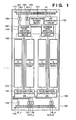
- Fig. 1 is a diagram for describing the structure of the ink-jet printhead according to the first embodiment.
- Reference numeral 100 denotes a substrate in which heaters and driving circuits have been built in by a semiconductor process technology. This substrate corresponds to the above-described substrate 1705 for an ink-jet printhead.
- Reference 102 denotes an ink supply port (that is, the supply path) for supplying ink from the reverse side of the substrate, 101 a heater/driver array in which a plurality of heaters and driver circuits are arrayed, wherein the heaters are electrothermal transducers for discharging ink and the drivers are for selectively driving the heaters.
- Reference numeral 103 denotes a shift register, which possesses data corresponding to one block of time-division drive, for temporarily holding print data to be printed, 107 a decoder circuit for selecting and driving the heaters in the heater/driver array on a per-heater-block basis, 104 an input circuit that includes a buffer circuit for inputting a digital signal to the shift register 103 and decoder 107, and 110 an input terminal.
- reference numeral 130 denotes a VHT voltage generating circuit for generating a VHT voltage, which is supplied to a pulse-amplitude converting circuit, based upon a heater-driving power-supply voltage (VH), and 140 a pulse-amplitude converting circuit for converting a digital signal having a VDD voltage amplitude to a gate driving pulse of a driver transistor having the VHT voltage amplitude.
- VH heater-driving power-supply voltage
- the pulse-amplitude converting circuit 140 of this embodiment is provided in an output stage of the decoder circuit 107 and in the output stage of the shift register 103.
- Reference numeral 121 denotes a temperature sensing block constructed to include an element for sensing the temperature of the semiconductor substrate 100.
- the temperature sensing block 121 for sensing the temperature of the substrate is exemplified as an element for monitoring the state of the substrate, it may be equipped with an element for sensing the resistance value of an electrothermal transducer or an element for sensing the resistance value of the current driving transistor at the time of operation thereof. It goes without saying that sensing elements of a plurality of types may be provided.
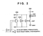
- Fig. 2 is one segment's worth of an equivalent circuit diagram for supplying current to and driving a heater for discharging ink in the first embodiment.
- Fig. 3 is an equivalent circuit that corresponds to one bit of a shift register and latch circuit for temporarily storing image data to be printed.
- the pulse amplitude converting circuit which was provided for each segment (each heating resistor for discharging ink) in the conventional circuit described with reference to Figs. 5 and 6A , is provided in the output section of the shift register 103 and of the decoder 107 on the substrate 100 for the ink-jet printhead of this embodiment. That is, here a structure is adopted in which a pulse-amplitude voltage is raised before the AND is taken between the output signal (block select signal) of the decoder circuit 107 and the output signal (bit signal) of the shift register 103. As a result, as shown in Fig. 2 , a pulse whose amplitude has already risen to the VHT voltage is supplied to each segment, and a converting circuit is no longer necessary. Area on the substrate taken up by elements of the circuit therefore is unnecessary.
- each individual transistor is larger than a low-voltage transistor.
- the number of pulse-amplitude converting circuits can be reduced and, with regard to layout location, they can be placed at positions spaced away from the vicinity of each element. As a result, the overall size of the substrate 100 for the ink-jet printhead can be reduced.
- Fig. 3 is a diagram illustrating the structure of the shift register 103 and pulse-amplitude converting circuit 140 according to this embodiment.
- the pulse-amplitude converting circuit is provided in the output stage in the shift-register circuit arrangement illustrated in Fig. 6B .
- the pulse amplitude is converted from the VDD voltage to the VHT voltage.
- Fig. 4 is a diagram useful in describing a substrate for an ink-jet printhead according to a second embodiment.
- Components in Fig. 4 identical with those in Fig. 1 are designated by like reference numerals and a detailed description thereof is omitted.
- the configuration adopted is one in which the pulse-amplitude converting circuit 140 is inserted immediately following the input circuit 104.
- the pulse-amplitude converting circuit 140 is inserted immediately following the input circuit 104.
- a circuit arrangement in which a voltage for driving logic is converted to a voltage for driving elements without increasing the length of segments in a direction perpendicular to the array direction of the segments. Further, according to the present invention, pulse-amplitude converting circuits are reduced and the number of elements formed on the substrate is reduced, thereby making it possible to raise yield and simplify circuit structure.
Landscapes
- Engineering & Computer Science (AREA)
- Microelectronics & Electronic Packaging (AREA)
- Particle Formation And Scattering Control In Inkjet Printers (AREA)
- Ink Jet (AREA)
Abstract
Description
- This invention relates an ink-jet printhead substrate, an ink-jet printhead and a printing apparatus that uses this printhead. More particularly, the invention relates to an ink-jet printhead in which electrothermal transducers for generating thermal energy necessary to discharge ink and driving circuits for driving the transducers are formed on the same substrate, and to a printing apparatus that uses this printhead.
- In general, an electrothermal transducer (heater) of a printhead mounted on a printing apparatus in accordance with an ink-jet scheme and the driving circuit of the transducer are formed on the same substrate using semiconductor process technology as illustrated in, e.g.,
USP 6,290,334 andUS 6,435,668 . In a proposed printhead structure, a digital circuit, etc., for sensing the state of the semiconductor substrate, e.g., the substrate temperature, is formed on the same substrate in addition to the driving circuit, an ink supply port is located at the center of the substrate and a heater is disposed at a position opposing the port. -
Fig. 5 is a diagram schematically illustrating a semiconductor substrate for an ink-jet printhead of this type, i.e., a semiconductor substrate for an ink-jet printhead that includes a circuit for outputting a digital signal indicative of sensed temperature. - In
Fig. 5 ,reference numeral 500 denotes a substrate obtained by integrally forming heaters and driving circuits by semiconductor process technology, 501 a heater/driver array having a structure in which a plurality of heaters and driver circuits are arrayed, and 502 an ink supply port for supplying ink from the reverse side of the substrate. - Further,
reference numeral 503 denotes a shift register for temporarily holding print data to be printed.Reference numeral 507 denotes a decoder circuit that outputs a heater-block selection signal for driving the heaters in the heater/driver array 501 on a per-heater-block basis.Reference numeral 504 denotes an input circuit that includes a buffer circuit for inputting a digital signal to theshift register 503 anddecoder 507.Reference numeral 510 denotes an input terminal that includes a terminal for supplying logic-element voltage VDD, a terminal CLK for inputting a clock and a terminal for inputting print data, etc. -
Fig. 7 is a timing chart for describing a series of operations up to sending of print information to theshift register 503 and supplying of current to heaters to drive the same. - Print data is supplied to DATA_A and DATA_B terminals in sync with a clock pulse applied to the CLK terminal. The
shift register 503 stores the supplied print data temporarily and a latch circuit latches the print data in response to a latch signal applied to a BG terminal. A block signal, which is for selecting a group of heaters that have been partitioned into a desired block, and the print data that has been latched by the latch signal are subsequently subjected to an AND operation in matrix form, and the heater current flows in sync with an HE signal that directly decides current drive time. This series of operations is repeated block by block to perform printing. -
Fig. 6A is one segment's worth of an equivalent circuit for driving current into a heater for discharging ink. Further,Fig. 6B is an equivalent circuit that corresponds to one bit of a shift register and latch circuit for temporarily storing image data to be printed. - A block select signal that is input to an
AND gate 601 is a signal sent from thedecoder 507 for selecting heater groups partitioned into blocks. Further, a bit signal that enters theAND gate 601 is a signal transferred to theshift register 503 and thenceforth latched by a latch signal. In order to turn on each segment selectively by print data, theAND gate 601 obtains the AND, in matrix form, between the block select signal and bit signal. -
Reference numeral 605 denotes a VH power-supply line that serves as a power supply for heater drive, 606 a heater and 607 a driver transistor for passing current into theheater 606.Reference numeral 602 denotes an inverter circuit for receiving and buffering the output of theAND gate 601.Reference numeral 603 denotes a VDD power-supply line that serves as a power supply for theinverter circuit 602.Reference numeral 608 denotes an inverter circuit serving as a buffer for receiving the buffered output of theinverter circuit 602.Reference numeral 604 denotes a VHT power-supply line serving as a power supply, which is supplied to abuffer 608, for supplying the gate voltage of the driver transistor. - In general, the
inverter 602 andshift register 503, etc., are digital circuits and they basically operate in accordance with low/high pulses. Further, applied pulses for interfacing print information of the printhead per se and for driving the heaters also are digital signals, and an exchange of signals with the outside is performed in its entirety by low/high logic pulses. Generally the amplitudes of these logic pulses are 0V/5V or 0V/3.3V, and the power supply VDD of the digital circuits is supplied with a signal one of these voltages. Accordingly, pulses having the amplitude of the VDD voltage are input to theAND gate 601 and are input to theinverter circuit 608 of the next stage through a buffer constituted by the two-stage inverter circuit 602. - On the other hand, the smaller the resistance value of the
driver transistor 607 when the latter is in the ON state, or the so-called ON resistance, the better. By making power consumed by components other than the heaters as small as possible, a rise in substrate temperature can be prevented and it is possible to drive the printhead stably. If the ON resistance of thedriver transistor 607 is large, a voltage drop ascribable to heater current that flows through this portion increases and it becomes necessary to apply an excessively high voltage to the heaters. The result is wasteful power consumption. - In order to reduce the ON voltage of the
driver transistor 607, the voltage applied to the gate of this transistor is required to be set high. In the circuit illustrated inFig. 6A , therefore, it becomes necessary to provide a circuit for making a conversion to pulses having a voltage amplitude higher than the voltage VDD. In the circuit shown inFig. 6A , the power-supply line 604 of voltage VHT higher than voltage VDD is provided and a segment selection signal that has entered in response to the pulse having the amplitude of the voltage VDD is converted to a pulse having the amplitude of voltage VHT by a buffer circuit that includes theinverter circuit 608. After the conversion is thus made to the pulse having the amplitude of voltage VHT, the pulse is applied to the gate of thedriver transistor 607. In other words, an arrangement is adopted in which the exchange of signals with the outside and signal processing by the internal digital circuit are performed in their entirety by pulses having the voltage amplitude (voltage for driving the logic circuits) of VDD, and each segment is provided with a circuit (pulse-amplitude converting circuit) for effecting a conversion to pulses of the VHT voltage amplitude (the voltage for element drive) immediately before the gate ofdriver transistor 607 is driven. - In general, a printhead takes on a form in which a plurality of individual segments are arrayed at a high density, and therefore in a case where the segments are arrayed at a density of, e.g., 600 dpi, segment width in the array direction is limited to about 42.3 µm. If it is attempted to fit the entirety of the circuit of the kind shown in
Fig. 6A in this pitch for driving each of the elements, then the length of each segment will increase in a direction perpendicular to the array direction. -
Fig. 10 is a circuit diagram of an equivalent circuit in a case where the pulse-amplitude converting circuit inFig. 6A is shown in detail. It will be understood from observing this diagram that the pulse-amplitude converting circuit, particularly a level converter indicated by the dashed lines, is composed of a number of transistors, and therefore a greater chip area becomes necessary. - However, when the layout structure of the printhead substrate having the above-described construction is considered, the pulse-amplitude converting circuit provided for each segment leads to an increase in the length of each segment, invites an increase in chip size and raises cost. More specifically, with the above-described layout, the chip becomes larger in a direction perpendicular to the segment array and the increase in chip size becomes pronounced. Further, in a case where the pulse-amplitude converting circuit is provided for every segment, e.g., in a case where consideration is given to a printhead having, e.g., 256 segments, the number of buffer circuits required necessitates at least 256 inverters. This invites a decline in yield and in a more complicated circuit structure and is a cause of higher cost.
- The present invention has been devised in view of the foregoing problems and its object is to provide a circuit arrangement in which a voltage for driving logic is converted to a voltage for driving elements without increasing the length of segments in a direction perpendicular to the array direction of the segments.
- Another object of the present invention is to reduce pulse-amplitude converting circuits and reduce the number of elements formed on the substrate, thereby raising yield and simplifying circuit structure.
- The above objects are achieved by the ink-jet printhead substrate according to
claim 1 , the controlling method according to claim 10 the ink-jet printhead according to claim 11, the ink-jet printhead cartridge according to claim 12 and the ink-jet printing apparatus according to claim 13. The other claims relate to further developments. - Other features and advantages of the present invention will be apparent from the following description taken in conjunction with the accompanying drawings, in which like reference characters designate the same or similar parts throughout the figures thereof.
- The accompanying drawings, which are incorporated in and constitute a part of the specification, illustrate embodiments of the invention and, together with the description, serve to explain the principles of the invention.
-
Fig. 1 is a diagram useful in describing the structure of an ink-jet printhead according to a first embodiment; -
Fig. 2 is one segment's worth of an equivalent circuit diagram for supplying current to and driving a heater for discharging ink in the first embodiment; -
Fig. 3 is a diagram illustrating the structure of ashift register 103 according to this embodiment; -
Fig. 4 is a diagram useful in describing a substrate for an ink-jet printhead according to a second embodiment; -
Fig. 5 is a diagram schematically illustrating a semiconductor substrate for an ink-jet printhead, namely a semiconductor substrate for an ink-jet printhead that includes a circuit for outputting a digital signal indicative of sensed temperature; -
Fig. 6A is one segment's worth of an equivalent circuit diagram for driving current into a heater for discharging ink; -
Fig. 6B is an equivalent circuit that corresponds to one bit of a shift register and latch circuit for temporarily storing image data to be printed; -
Fig. 7 is a timing chart for describing a series of operations up to sending of print information to theshift register 503 and supplying of current to heaters to drive the same; -
Fig. 8 is an external view of an ink-jet printing apparatus to which the present invention is applicable; -
Fig. 9 is a diagram illustrating a control - arrangement for executing control of printing by the ink-jet printing apparatus shown inFig. 8 ; and -
Fig. 10 is a diagram illustrating an equivalent circuit of a pulse-amplitude converting circuit. -
Fig. 11 is a perspective view showing a detailed outer appearance of an inkjet cartridge IJC; and -
Fig. 12 is a perspective view showing a three-dimensional structure of a printhead IJHC that discharges three colors of ink. - Preferred embodiments of the present invention will now be described in detail with the accompanying drawings.
- The term "print" used in the present invention signifies not only imparting an image having the meaning of text or graphics to a printing medium but also imparting an image that does not have the meaning of a pattern or the like.
- The term "substrate" used below not only refers to a simple substrate comprising a silicon semiconductor but also to a substrate that has been provided with various elements, circuits and wiring.
- It should be noted that the substrate made have the shape of a board or chip.
- The expression "on the substrate" not only refers simply to the top of the substrate but also to the surface of the substrate and the interior of the substrate in the vicinity of the surface. Further, "built-in" used in the present invention refers not only to the simple placing of separate elements on the substrate but also to the formation and manufacture of elements on the substrate as an integral part thereof by a semiconductor-circuit manufacturing process or the like.
- With the substrate for an ink-jet printhead of the embodiment described below, voltage conversion of pulse amplitude that was performed immediately prior to input to the gate terminal of the
driver transistor 607 is carried out before taking the AND between decoder output (Block Select) and shift-register output (BIT) on a per-segment basis. Further, a voltage higher than the logic voltage is applied to the part of the circuit that takes the AND on a per-segment basis. In the present embodiments, therefore, the element of this portion is made a transistor of a higher withstand voltage than that of the other logic circuits, namely decoders and shift registers (S/R). By virtue of this arrangement, a segment selection signal that has been input in response to a pulse having the amplitude of a VDD voltage can be converted to a pulse having the amplitude of VHT voltage without increasing the length of each segment in a direction perpendicular to the array direction of the segments. In particular, with the arrangement of the present embodiments, conversion of pulse width is performed before the AND is taken between the output signal from the decoder side and the signal from the side of the shift register, and therefore a pulse-amplitude converting circuit provided for every segment is no longer necessary. The number of pulse-amplitude converting circuits themselves can be reduced to the sum of the number of time-division drive blocks (the number of signal outputs from the decoder) and the number of data items corresponding to each block (the number of outputs from the shift register), yield is raised and the circuit arrangement is simplified. - First, an overview of an ink-jet printing apparatus will be described
-
Fig. 8 is an external view of an ink-jet printing apparatus to which the present invention is applicable. InFig. 8 , alead screw 5005 rotates via driving force transmission gears 5011, 5009 in operative association with the forward and reverse rotation of adriver motor 5013. A carriage HC has a pin (not shown) that mates with ahelical groove 5005 of thelead screw 5004 and that is moved back and forth in directions of arrows a and b as thelead screw 5004 rotates. An ink-jet cartridge IJC is mounted on the carriage- HC. -
Reference numeral 5002 denotes a paper retaining plate which presses paper against aplaten 5000 along the traveling direction of the carriage.Reference numerals carriage lever 5006 in the vicinity of the photosensors and changing over the direction in which themotor 5013 is rotated.Reference numeral 5016 denotes a member which supports acap member 5022, which is for capping the front side of the printhead.Reference numeral 5015 denotes suction means for applying suction to the cap. The suction means subjects the cap to suction recovery via anopening 5023 inside the cap. Reference numeral denotes a cleaning blade, andreference numeral 5019 denotes a member which makes it possible to move the blade back and forth. These are supported on asupport plate 5018 of the main body. It goes without saying that the blade need not be of this form and that a well-known cleaning blade can be applied to this example.Reference numeral 5021 denotes a lever for starting the suction of the suction recovery operation. The lever moves with movement of acam 5020 engaged with the carriage. Movement is controlled by well-known transmission means whereby the driving force from the driver motor is changed over as by a clutch. - It is so arranged that the capping, cleaning and suction recovery are carried out by desired processing at the corresponding positions by operation of the
lead screw 5004 when the carriage has arrived in the area on the home-position side. However, if it so arranged that a desired operation is carried out at a well-known timing any is applicable to this example. - Reference will now be had to the block diagram of
Fig. 9 to described a control arrangement for executing printing control of the above-described ink-jet printing apparatus. In this diagram illustrating a control circuit,reference numeral 1700 denotes an interface, 1701 an MPU, 1702 a program ROM for storing a control program executed by theMPU 1701, and 1703 a dynamic-type RAM (DRAM below) for storing various data (such as the above-mentioned print signal as well as print data supplied to the head) in advance.Reference numeral 1704 denotes a gate array for controlling supply of print data to theprinthead 1708. A signal for driving the printhead is supplied via this gate array. Further, the gate array controls transfer of data between theinterface 1700,MPU 1701 andRAM 1703. -
Reference 1710 denotes a carrier motor for transporting theprinthead 1708, and 1709 atransport motor 1709 for transporting printing paper.Reference numeral 1704 denotes an ink-jet printhead substrate mounted on theprinthead 1708 and including an ink-discharge heater and its drive circuit.Reference numerals transport motor 1709 andcarrier motor 1710, respectively. - Operation of the above-described control arrangement will now be described. When a print signal enters the
interface 1700, the print signal is converted to print data for printing between thegate array 1704 andMPU 1701. Themotor drivers printhead 1708. -
Fig. 11 is a perspective view showing a detailed outer appearance of the configuration of an inkjet cartridge IJC. - As shown in
Fig. 11 , the inkjet cartridge IJC is comprised of a cartridge IJCK that discharges black ink and a cartridge IJCC that discharges three colors of ink, cyan (C), magenta (M) and yellow (Y). These two cartridges are mutually separable, with each being independently detachably mounted on the carriage HC. - The cartridge IJCK is comprised of an ink tank ITK that contains black ink and a printhead IJHK that prints by discharging black ink, combined in an integrated structure. Similarly, the cartridge IJCC is comprised of an ink tank ITC that contains ink of three colors, cyan (C), magenta (M) and yellow (Y), and a printhead IJHC that prints by discharging ink of these colors, combined in an integrated structure.
- Further, as can be appreciated from
Fig. 11 , an array of nozzles that discharges black ink, an array of nozzles that discharges cyan ink, an array of nozzles that discharges magenta ink and an array of nozzles that discharges yellow ink are aligned in a direction of movement of the carriage, the arrayed direction of the nozzles being disposed perpendicular to the carriage movement direction. -
Fig. 12 is a perspective view showing a three-dimensional structure of a printhead IJHC that discharges three colors of ink. -
Fig. 12 shows the flow of ink supplied from the ink tank ITK. The printhead IJHC has anink channel 2C that supplies cyan (C) ink, anink channel 2M that supplies magenta (M) ink, and anink channel 2Y that supplies yellow (Y) ink, and is provided with supply paths (not shown), that supply each of the inks via a rear surface of the substrate from the ink tank ITK to each of the ink channels. - The cyan, magenta and yellow inks that pass through the ink channels
ink flow paths ink droplets orifices - It should be noted that, in
Fig. 12 ,reference numeral 1 denotes a printhead substrate (hereinafter referred to as "substrate") on which are formed electrothermal transducers and the variety of circuits that drive the electrothermal transducers to be described later, a memory, a variety of pads that form the electrical contacts with the carriage HC, and a variety of signal wires. - Moreover, one electrothermal transducer (heater), the MOS-FET that drives it and the electrothermal transducer (heater) are together called a printing element, with a plurality of printing elements called a printing element.
- Note that although
Fig. 12 is a diagram showing a three dimensional structure of a printhead IJHC that discharges three colors of ink, the structure is the same as that of the printhead IJHK that discharges black ink but comprising one third of the configuration shown inFig. 12 . In other words, there is one ink channel, and the scale of the printhead is approximately one third that of the structure shown inFig. 12 . -
Fig. 1 is a diagram for describing the structure of the ink-jet printhead according to the first embodiment.Reference numeral 100 denotes a substrate in which heaters and driving circuits have been built in by a semiconductor process technology. This substrate corresponds to the above-describedsubstrate 1705 for an ink-jet printhead.Reference 102 denotes an ink supply port (that is, the supply path) for supplying ink from the reverse side of the substrate, 101 a heater/driver array in which a plurality of heaters and driver circuits are arrayed, wherein the heaters are electrothermal transducers for discharging ink and the drivers are for selectively driving the heaters.Reference numeral 103 denotes a shift register, which possesses data corresponding to one block of time-division drive, for temporarily holding print data to be printed, 107 a decoder circuit for selecting and driving the heaters in the heater/driver array on a per-heater-block basis, 104 an input circuit that includes a buffer circuit for inputting a digital signal to theshift register 103 anddecoder - Further,
reference numeral 130 denotes a VHT voltage generating circuit for generating a VHT voltage, which is supplied to a pulse-amplitude converting circuit, based upon a heater-driving power-supply voltage (VH), and 140 a pulse-amplitude converting circuit for converting a digital signal having a VDD voltage amplitude to a gate driving pulse of a driver transistor having the VHT voltage amplitude. As will be understood fromFig. 1 , the pulse-amplitude converting circuit 140 of this embodiment is provided in an output stage of thedecoder circuit 107 and in the output stage of theshift register 103. -
Reference numeral 121 denotes a temperature sensing block constructed to include an element for sensing the temperature of thesemiconductor substrate 100. Though thetemperature sensing block 121 for sensing the temperature of the substrate is exemplified as an element for monitoring the state of the substrate, it may be equipped with an element for sensing the resistance value of an electrothermal transducer or an element for sensing the resistance value of the current driving transistor at the time of operation thereof. It goes without saying that sensing elements of a plurality of types may be provided. -
Fig. 2 is one segment's worth of an equivalent circuit diagram for supplying current to and driving a heater for discharging ink in the first embodiment. Further,Fig. 3 is an equivalent circuit that corresponds to one bit of a shift register and latch circuit for temporarily storing image data to be printed. - As shown in
Fig. 1 , the pulse amplitude converting circuit, which was provided for each segment (each heating resistor for discharging ink) in the conventional circuit described with reference toFigs. 5 and6A , is provided in the output section of theshift register 103 and of thedecoder 107 on thesubstrate 100 for the ink-jet printhead of this embodiment. That is, here a structure is adopted in which a pulse-amplitude voltage is raised before the AND is taken between the output signal (block select signal) of thedecoder circuit 107 and the output signal (bit signal) of theshift register 103. As a result, as shown inFig. 2 , a pulse whose amplitude has already risen to the VHT voltage is supplied to each segment, and a converting circuit is no longer necessary. Area on the substrate taken up by elements of the circuit therefore is unnecessary. - Since the arrangement is such that a high voltage is applied to the AND
gate 201 that takes the AND segment by segment, an element of a high withstand voltage is required for the transistor constructing this circuit. In the prior art, only a low voltage corresponding to the logic voltage is applied to this portion and therefore the transistor is constructed by an element of low withstand voltage. In this embodiment, however, the goal is achieved by giving this portion a withstand voltage higher than that of the transistors constructing the other logic circuits, or more specifically, by adopting an element having a high withstand voltage for the transistor that constructs the AND gate. - In a case where a transistor (MOS transistor) with a high withstand voltage is used, each individual transistor is larger than a low-voltage transistor. However, as mentioned above, the number of pulse-amplitude converting circuits (booster circuits) can be reduced and, with regard to layout location, they can be placed at positions spaced away from the vicinity of each element. As a result, the overall size of the
substrate 100 for the ink-jet printhead can be reduced. -
Fig. 3 is a diagram illustrating the structure of theshift register 103 and pulse-amplitude converting circuit 140 according to this embodiment. The pulse-amplitude converting circuit is provided in the output stage in the shift-register circuit arrangement illustrated inFig. 6B . Here the pulse amplitude is converted from the VDD voltage to the VHT voltage. - The number of output stages of the
shift register 103 anddecoder circuit 107 is decided by the number of divisions when all segments are driven in time-shared fashion, though division is roughly on the order of 8 to 32. For example, if 256 segments are divided by 16 (each block will have 16 segments), the number of pulse-amplitude converting circuits necessary will be 16 x 2 (shift-register side and decoder side) = 32. This is a major reduction in comparison with the 256 circuits needed when all segments are provided with the pulse-amplitude converting circuits. As a result, chip length in the direction perpendicular to the segment array direction can be reduced. Further, though length of the chip in the array direction is increased owing to the pulse-amplitude converting circuit added onto theshift register 103 anddecoder circuit 107, this is a very small increase in comparison with the reduction in length in the perpendicular direction and there is a reduction in terms of total chip area. -
Fig. 4 is a diagram useful in describing a substrate for an ink-jet printhead according to a second embodiment. Components inFig. 4 identical with those inFig. 1 are designated by like reference numerals and a detailed description thereof is omitted. - In the second embodiment, the configuration adopted is one in which the pulse-
amplitude converting circuit 140 is inserted immediately following theinput circuit 104. By virtue of this configuration, only pulse-amplitude converting circuits the number of which is equivalent to the number of input terminals (CLK, DATA_A, DATA_B, BG, HE_A, HE_B) are required.
This makes it possible to realize an even greater reduction in chip size. - In accordance with each of the above-described embodiments, as described above, voltage conversion of pulse amplitude that was performed immediately prior to input to the gate terminal of the driver transistor in the prior art is carried out before taking the AND between decoder output and shift-register output. As a result, a circuit structure is implemented in which a segment selection signal that has been input in response to a pulse having the amplitude of VDD voltage is converted to a pulse having the amplitude of VHT voltage without increasing the length of each segment in a direction perpendicular to the array direction of the segments. Also, a circuit structure is implemented in which the number of pulse-amplitude converting circuits is remarkably reduced. Consequently, chip size is reduced, yield is improved by reducing the number of elements and lower cost can be expected owing to simplification of circuit structure.
- In accordance with the present invention, as described above, there can be provided a circuit arrangement in which a voltage for driving logic is converted to a voltage for driving elements without increasing the length of segments in a direction perpendicular to the array direction of the segments. Further, according to the present invention, pulse-amplitude converting circuits are reduced and the number of elements formed on the substrate is reduced, thereby making it possible to raise yield and simplify circuit structure.
- As many different embodiments of the present invention can be made without departing from the scope thereof, it is to be understood that the invention is not limited to the specific embodiments thereof except as defined in the appended claims.
Claims (14)
- An ink-jet printhead substrate (1, 100, 1705) on which are mounted electrothermal transducers (206, 606) for generating thermal energy utilized to discharge ink and driver circuits (207, 607) for driving said electrothermal transducers, characterized by comprising:a logic circuit (103, 104, 107, 110, 140) for separately outputting, based upon an input signal of a first voltage amplitude level (VDD), a block selection signal and an element driving signal which are output for each electrothermal transducer in a selected block at a second voltage amplitude level (VHT), the second voltage amplitude level being higher than the first voltage amplitude level; anda driver circuit (201, 204, 205, 208) for driving the electrothermal transducers in block units based upon the block selection signal and element driving signal received from said logic circuit.
- The ink-jet printhead substrate according to claim 1, wherein said logic circuit comprises:a first converting circuit (103, 104, 107, 110) for converting the input signal of the first voltage amplitude level separately to the block selection signal and to the element driving signal of the first voltage amplitude level; anda second converting circuit (140) for separately converting the block selection signal and element driving signal, which are output from said first converting circuit, to the second voltage amplitude level.
- The ink-jet printhead substrate according to claim 1, wherein said logic circuit comprises:a first converting circuit (103, 104, 110, 140) for converting the input signal of the first voltage amplitude level to the second voltage amplitude level; anda second converting circuit (107) for separately generating the block selection signal of the second voltage amplitude level and the element driving circuit for the selected block from an input signal of the second voltage amplitude level obtained from said first converting circuit.
- The ink-jet printhead substrate according to any one of claims 1 to 3, further comprising a monitor element for sensing a state of said semiconductor substrate.
- The ink-jet printhead substrate according to claim 4, wherein said state is one of a resistance of the electrochemical transducer or a resistance of the current driving transistor at a time of operation.
- The ink-jet printhead substrate according to claim 1, wherein said logic circuit includes a shift register circuit, a decoder circuit and a converting circuit for converting signals output from said shift register circuit and said decoder circuit into signals having the second voltage amplitude level.
- The ink-jet printhead substrate according to claim 6, wherein a withstand voltage of a transistor constituting said driver circuit is higher than that of a transistor constituting said shift register circuit and said decoder circuit in said logic circuits.
- The ink-jet printhead substrate according to claim 6, further comprising a voltage generating circuit for generating a voltage to be supplied to said conversion circuit based on a voltage supplied to said electrothermal transducers.
- The ink-jet printhead substrate according to claim 1, wherein said substrate has an ink supply port for supplying ink, and said electrothermal transducers and said driver circuit are arrayed along said ink supply port.
- A method of controlling drive of electrothermal transducers on a substrate (1, 100, 1705) on which are mounted electrothermal transducers (206, 606) for generating thermal energy utilized to discharge ink and driver circuits for driving said electrothermal transducers, said method being characterized by comprising the steps of:inputting an input signal of a first voltage amplitude level (VDD);separately outputting, based upon the signal that has been input, a block selection signal and an element driving signal which are output for each electrothermal transducer in a selected block at a second voltage amplitude level (VHT), the second voltage amplitude level being higher than the first voltage amplitude level; anddriving the electrothermal transducers in block units based upon the block selection signal and element driving signal received from said logic circuit.
- An ink-jet printhead comprising:discharge ports (102) for discharging ink; andthe substrate according to any one of claims 1 to 9 on which are mounted electrothermal transducers provided to correspond to said discharge ports, and driver circuits for driving said electrothermal transducers.
- An ink-jet printhead cartridge comprising the ink-jet printhead according to claim 11 and an ink tank filled with ink for being supplied to said ink-jet printhead.
- An ink-jet printing apparatus comprising an ink-jet printhead according to claim 11 and a circuit for transmitting a control signal to said printhead.
- An ink-jet printing apparatus comprising an ink-jet printhead cartridge according to claim 12.
Applications Claiming Priority (2)
| Application Number | Priority Date | Filing Date | Title |
|---|---|---|---|
| JP2003165028 | 2003-06-10 | ||
| PCT/JP2004/007879 WO2004110764A1 (en) | 2003-06-10 | 2004-06-01 | Ink-jet printhead substrate, driving control method, ink-jet printhead and ink-jet printing apparatus |
Publications (2)
| Publication Number | Publication Date |
|---|---|
| EP1636036A1 EP1636036A1 (en) | 2006-03-22 |
| EP1636036B1 true EP1636036B1 (en) | 2008-12-24 |
Family
ID=33549199
Family Applications (1)
| Application Number | Title | Priority Date | Filing Date |
|---|---|---|---|
| EP04735669A Expired - Lifetime EP1636036B1 (en) | 2003-06-10 | 2004-06-01 | Ink-jet printhead substrate, driving control method, ink-jet printhead and ink-jet printing apparatus |
Country Status (9)
| Country | Link |
|---|---|
| US (1) | US7267429B2 (en) |
| EP (1) | EP1636036B1 (en) |
| KR (1) | KR100776973B1 (en) |
| CN (2) | CN101239531B (en) |
| AT (1) | ATE418456T1 (en) |
| DE (1) | DE602004018638D1 (en) |
| RU (1) | RU2326003C2 (en) |
| TW (1) | TWI246462B (en) |
| WO (1) | WO2004110764A1 (en) |
Families Citing this family (14)
| Publication number | Priority date | Publication date | Assignee | Title |
|---|---|---|---|---|
| KR100757861B1 (en) * | 2004-07-21 | 2007-09-11 | 삼성전자주식회사 | ink jet head substrate, ink jet head and method for manufacturing ink jet head substrate |
| JP4785375B2 (en) * | 2004-12-09 | 2011-10-05 | キヤノン株式会社 | Inkjet recording head substrate, recording head, head cartridge, and recording apparatus |
| US7559626B2 (en) * | 2004-12-09 | 2009-07-14 | Canon Kabushiki Kaisha | Inkjet recording head substrate and drive control method, inkjet recording head, inkjet recording head cartridge and inkjet recording apparatus |
| TWI296573B (en) | 2005-06-16 | 2008-05-11 | Canon Kk | Element body for recording head and recording head having element body |
| DE602007008808D1 (en) * | 2006-10-04 | 2010-10-14 | Canon Kk | Component carrier, printhead and head cartridge with the component carrier |
| JP5183181B2 (en) | 2007-12-11 | 2013-04-17 | キヤノン株式会社 | Inkjet recording head |
| JP5534740B2 (en) * | 2008-08-29 | 2014-07-02 | キヤノン株式会社 | Substrate for liquid discharge head and liquid discharge head using the same |
| JP5723137B2 (en) * | 2009-11-26 | 2015-05-27 | キヤノン株式会社 | Printhead substrate, printhead, and printing apparatus |
| JP5713728B2 (en) * | 2010-04-01 | 2015-05-07 | キヤノン株式会社 | Recording head |
| JP5981815B2 (en) * | 2012-09-18 | 2016-08-31 | キヤノン株式会社 | Printhead substrate and printing apparatus |
| JP6971903B2 (en) | 2018-03-29 | 2021-11-24 | キヤノン株式会社 | Inspection method for recording devices and recording heads |
| BR112021014334A2 (en) | 2019-02-06 | 2021-09-21 | Hewlett-Packard Development Company, L.P. | MATRIX FOR A PRINT HEAD |
| CN113396065B (en) | 2019-02-06 | 2022-11-18 | 惠普发展公司,有限责任合伙企业 | Die for a printhead, printhead including the die, and method of forming the die |
| PT3710260T (en) | 2019-02-06 | 2021-08-19 | Hewlett Packard Development Co | Die for a printhead |
Family Cites Families (10)
| Publication number | Priority date | Publication date | Assignee | Title |
|---|---|---|---|---|
| US5172134A (en) * | 1989-03-31 | 1992-12-15 | Canon Kabushiki Kaisha | Ink jet recording head, driving method for same and ink jet recording apparatus |
| CA2075097C (en) | 1991-08-02 | 2000-03-28 | Hiroyuki Ishinaga | Recording apparatus, recording head and substrate therefor |
| JP2000141660A (en) * | 1998-11-11 | 2000-05-23 | Canon Inc | Recording head and recorder employing it |
| US6435668B1 (en) * | 1999-02-19 | 2002-08-20 | Hewlett-Packard Company | Warming device for controlling the temperature of an inkjet printhead |
| JP2001063054A (en) | 1999-08-24 | 2001-03-13 | Canon Inc | Recording head and recording apparatus |
| JP3652274B2 (en) * | 2001-04-26 | 2005-05-25 | キヤノン株式会社 | Ink jet recording apparatus and recording apparatus control method |
| JP2002370348A (en) | 2001-06-15 | 2002-12-24 | Canon Inc | Substrate for recording head, recording head and recorder |
| JP2002370363A (en) * | 2001-06-15 | 2002-12-24 | Canon Inc | Substrate for ink jet recording head, ink jet recording head, and ink jet recorder |
| US7559626B2 (en) * | 2004-12-09 | 2009-07-14 | Canon Kabushiki Kaisha | Inkjet recording head substrate and drive control method, inkjet recording head, inkjet recording head cartridge and inkjet recording apparatus |
| JP4785375B2 (en) * | 2004-12-09 | 2011-10-05 | キヤノン株式会社 | Inkjet recording head substrate, recording head, head cartridge, and recording apparatus |
-
2004
- 2004-05-27 TW TW093115171A patent/TWI246462B/en not_active IP Right Cessation
- 2004-06-01 KR KR1020057023614A patent/KR100776973B1/en not_active IP Right Cessation
- 2004-06-01 RU RU2005141543/12A patent/RU2326003C2/en not_active IP Right Cessation
- 2004-06-01 DE DE602004018638T patent/DE602004018638D1/en not_active Expired - Lifetime
- 2004-06-01 AT AT04735669T patent/ATE418456T1/en not_active IP Right Cessation
- 2004-06-01 CN CN2008100094624A patent/CN101239531B/en not_active Expired - Fee Related
- 2004-06-01 CN CNB2004800161667A patent/CN100408337C/en not_active Expired - Fee Related
- 2004-06-01 EP EP04735669A patent/EP1636036B1/en not_active Expired - Lifetime
- 2004-06-01 US US10/555,304 patent/US7267429B2/en not_active Expired - Lifetime
- 2004-06-01 WO PCT/JP2004/007879 patent/WO2004110764A1/en active Application Filing
Also Published As
| Publication number | Publication date |
|---|---|
| US7267429B2 (en) | 2007-09-11 |
| CN101239531B (en) | 2011-11-23 |
| TWI246462B (en) | 2006-01-01 |
| RU2326003C2 (en) | 2008-06-10 |
| CN101239531A (en) | 2008-08-13 |
| DE602004018638D1 (en) | 2009-02-05 |
| TW200520965A (en) | 2005-07-01 |
| RU2005141543A (en) | 2006-05-10 |
| US20060209131A1 (en) | 2006-09-21 |
| CN1805854A (en) | 2006-07-19 |
| CN100408337C (en) | 2008-08-06 |
| EP1636036A1 (en) | 2006-03-22 |
| KR20060026868A (en) | 2006-03-24 |
| ATE418456T1 (en) | 2009-01-15 |
| KR100776973B1 (en) | 2007-11-21 |
| WO2004110764A1 (en) | 2004-12-23 |
Similar Documents
| Publication | Publication Date | Title |
|---|---|---|
| EP1899163B1 (en) | Head substrate, printhead, head cartridge, and printing apparatus | |
| EP1543972B1 (en) | Element board for printhead, and printhead having the same | |
| US8191996B2 (en) | Element substrate, and printhead, head cartridge, and printing apparatus using the element substrate | |
| EP1636036B1 (en) | Ink-jet printhead substrate, driving control method, ink-jet printhead and ink-jet printing apparatus | |
| KR20060049460A (en) | Printhead substrate, printhead, head cartridge, and printing apparatus | |
| KR100915246B1 (en) | Device substrate for recording head, recording head, and recording apparatus including the recording head | |
| KR100791851B1 (en) | Substrate for ink jet recording head, driving control method, ink jet recording head, and ink jet recording apparatus | |
| JP2006007763A (en) | Substrate for recording head, recording head, head cartridge, and recorder | |
| KR20060049459A (en) | Printhead substrate, printhead, head cartridge, and printing apparatus | |
| JP2007022069A (en) | Element substrate of recording head, recording head, recording device and recording head cartridge | |
| US7588304B2 (en) | Liquid discharge head substrate, liquid discharge head, and liquid discharge apparatus | |
| JP4678825B2 (en) | Head substrate, recording head, head cartridge, and recording apparatus using the recording head or head cartridge | |
| JP5031455B2 (en) | Element substrate for recording head, recording head, and recording apparatus using the recording head | |
| JP3997217B2 (en) | Inkjet recording head substrate, drive control method, inkjet recording head, and inkjet recording apparatus | |
| JP2006007762A (en) | Substrate for recording head, recording head, head cartridge, and recorder | |
| JP2004306564A (en) | Substrate for recording head, recording head, temperature control method for recording head, and recording device | |
| JP2006007761A (en) | Substrate for recording head, recording head, head cartridge and recorder |
Legal Events
| Date | Code | Title | Description |
|---|---|---|---|
| PUAI | Public reference made under article 153(3) epc to a published international application that has entered the european phase |
Free format text: ORIGINAL CODE: 0009012 |
|
| 17P | Request for examination filed |
Effective date: 20060110 |
|
| AK | Designated contracting states |
Kind code of ref document: A1 Designated state(s): AT BE BG CH CY CZ DE DK EE ES FI FR GB GR HU IE IT LI LU MC NL PL PT RO SE SI SK TR |
|
| DAX | Request for extension of the european patent (deleted) | ||
| 17Q | First examination report despatched |
Effective date: 20060908 |
|
| GRAP | Despatch of communication of intention to grant a patent |
Free format text: ORIGINAL CODE: EPIDOSNIGR1 |
|
| GRAS | Grant fee paid |
Free format text: ORIGINAL CODE: EPIDOSNIGR3 |
|
| GRAA | (expected) grant |
Free format text: ORIGINAL CODE: 0009210 |
|
| AK | Designated contracting states |
Kind code of ref document: B1 Designated state(s): AT BE BG CH CY CZ DE DK EE ES FI FR GB GR HU IE IT LI LU MC NL PL PT RO SE SI SK TR |
|
| REG | Reference to a national code |
Ref country code: GB Ref legal event code: FG4D |
|
| REG | Reference to a national code |
Ref country code: CH Ref legal event code: EP |
|
| REG | Reference to a national code |
Ref country code: IE Ref legal event code: FG4D |
|
| REF | Corresponds to: |
Ref document number: 602004018638 Country of ref document: DE Date of ref document: 20090205 Kind code of ref document: P |
|
| PG25 | Lapsed in a contracting state [announced via postgrant information from national office to epo] |
Ref country code: PL Free format text: LAPSE BECAUSE OF FAILURE TO SUBMIT A TRANSLATION OF THE DESCRIPTION OR TO PAY THE FEE WITHIN THE PRESCRIBED TIME-LIMIT Effective date: 20081224 Ref country code: FI Free format text: LAPSE BECAUSE OF FAILURE TO SUBMIT A TRANSLATION OF THE DESCRIPTION OR TO PAY THE FEE WITHIN THE PRESCRIBED TIME-LIMIT Effective date: 20081224 Ref country code: NL Free format text: LAPSE BECAUSE OF FAILURE TO SUBMIT A TRANSLATION OF THE DESCRIPTION OR TO PAY THE FEE WITHIN THE PRESCRIBED TIME-LIMIT Effective date: 20081224 Ref country code: SI Free format text: LAPSE BECAUSE OF FAILURE TO SUBMIT A TRANSLATION OF THE DESCRIPTION OR TO PAY THE FEE WITHIN THE PRESCRIBED TIME-LIMIT Effective date: 20081224 |
|
| NLV1 | Nl: lapsed or annulled due to failure to fulfill the requirements of art. 29p and 29m of the patents act | ||
| PG25 | Lapsed in a contracting state [announced via postgrant information from national office to epo] |
Ref country code: RO Free format text: LAPSE BECAUSE OF FAILURE TO SUBMIT A TRANSLATION OF THE DESCRIPTION OR TO PAY THE FEE WITHIN THE PRESCRIBED TIME-LIMIT Effective date: 20081224 Ref country code: ES Free format text: LAPSE BECAUSE OF FAILURE TO SUBMIT A TRANSLATION OF THE DESCRIPTION OR TO PAY THE FEE WITHIN THE PRESCRIBED TIME-LIMIT Effective date: 20090404 Ref country code: EE Free format text: LAPSE BECAUSE OF FAILURE TO SUBMIT A TRANSLATION OF THE DESCRIPTION OR TO PAY THE FEE WITHIN THE PRESCRIBED TIME-LIMIT Effective date: 20081224 Ref country code: BG Free format text: LAPSE BECAUSE OF FAILURE TO SUBMIT A TRANSLATION OF THE DESCRIPTION OR TO PAY THE FEE WITHIN THE PRESCRIBED TIME-LIMIT Effective date: 20090324 Ref country code: BE Free format text: LAPSE BECAUSE OF FAILURE TO SUBMIT A TRANSLATION OF THE DESCRIPTION OR TO PAY THE FEE WITHIN THE PRESCRIBED TIME-LIMIT Effective date: 20081224 |
|
| PG25 | Lapsed in a contracting state [announced via postgrant information from national office to epo] |
Ref country code: SE Free format text: LAPSE BECAUSE OF FAILURE TO SUBMIT A TRANSLATION OF THE DESCRIPTION OR TO PAY THE FEE WITHIN THE PRESCRIBED TIME-LIMIT Effective date: 20090324 Ref country code: PT Free format text: LAPSE BECAUSE OF FAILURE TO SUBMIT A TRANSLATION OF THE DESCRIPTION OR TO PAY THE FEE WITHIN THE PRESCRIBED TIME-LIMIT Effective date: 20090525 Ref country code: AT Free format text: LAPSE BECAUSE OF FAILURE TO SUBMIT A TRANSLATION OF THE DESCRIPTION OR TO PAY THE FEE WITHIN THE PRESCRIBED TIME-LIMIT Effective date: 20081224 Ref country code: CZ Free format text: LAPSE BECAUSE OF FAILURE TO SUBMIT A TRANSLATION OF THE DESCRIPTION OR TO PAY THE FEE WITHIN THE PRESCRIBED TIME-LIMIT Effective date: 20081224 |
|
| PG25 | Lapsed in a contracting state [announced via postgrant information from national office to epo] |
Ref country code: SK Free format text: LAPSE BECAUSE OF FAILURE TO SUBMIT A TRANSLATION OF THE DESCRIPTION OR TO PAY THE FEE WITHIN THE PRESCRIBED TIME-LIMIT Effective date: 20081224 |
|
| PG25 | Lapsed in a contracting state [announced via postgrant information from national office to epo] |
Ref country code: DK Free format text: LAPSE BECAUSE OF FAILURE TO SUBMIT A TRANSLATION OF THE DESCRIPTION OR TO PAY THE FEE WITHIN THE PRESCRIBED TIME-LIMIT Effective date: 20081224 |
|
| PLBE | No opposition filed within time limit |
Free format text: ORIGINAL CODE: 0009261 |
|
| STAA | Information on the status of an ep patent application or granted ep patent |
Free format text: STATUS: NO OPPOSITION FILED WITHIN TIME LIMIT |
|
| 26N | No opposition filed |
Effective date: 20090925 |
|
| PG25 | Lapsed in a contracting state [announced via postgrant information from national office to epo] |
Ref country code: MC Free format text: LAPSE BECAUSE OF NON-PAYMENT OF DUE FEES Effective date: 20090630 |
|
| REG | Reference to a national code |
Ref country code: CH Ref legal event code: PL |
|
| PG25 | Lapsed in a contracting state [announced via postgrant information from national office to epo] |
Ref country code: IE Free format text: LAPSE BECAUSE OF NON-PAYMENT OF DUE FEES Effective date: 20090601 Ref country code: LI Free format text: LAPSE BECAUSE OF NON-PAYMENT OF DUE FEES Effective date: 20090630 Ref country code: CH Free format text: LAPSE BECAUSE OF NON-PAYMENT OF DUE FEES Effective date: 20090630 |
|
| PG25 | Lapsed in a contracting state [announced via postgrant information from national office to epo] |
Ref country code: GR Free format text: LAPSE BECAUSE OF FAILURE TO SUBMIT A TRANSLATION OF THE DESCRIPTION OR TO PAY THE FEE WITHIN THE PRESCRIBED TIME-LIMIT Effective date: 20090325 |
|
| PG25 | Lapsed in a contracting state [announced via postgrant information from national office to epo] |
Ref country code: LU Free format text: LAPSE BECAUSE OF NON-PAYMENT OF DUE FEES Effective date: 20090601 |
|
| PG25 | Lapsed in a contracting state [announced via postgrant information from national office to epo] |
Ref country code: HU Free format text: LAPSE BECAUSE OF FAILURE TO SUBMIT A TRANSLATION OF THE DESCRIPTION OR TO PAY THE FEE WITHIN THE PRESCRIBED TIME-LIMIT Effective date: 20090625 |
|
| PG25 | Lapsed in a contracting state [announced via postgrant information from national office to epo] |
Ref country code: TR Free format text: LAPSE BECAUSE OF FAILURE TO SUBMIT A TRANSLATION OF THE DESCRIPTION OR TO PAY THE FEE WITHIN THE PRESCRIBED TIME-LIMIT Effective date: 20081224 |
|
| PG25 | Lapsed in a contracting state [announced via postgrant information from national office to epo] |
Ref country code: CY Free format text: LAPSE BECAUSE OF FAILURE TO SUBMIT A TRANSLATION OF THE DESCRIPTION OR TO PAY THE FEE WITHIN THE PRESCRIBED TIME-LIMIT Effective date: 20081224 |
|
| PGFP | Annual fee paid to national office [announced via postgrant information from national office to epo] |
Ref country code: IT Payment date: 20140604 Year of fee payment: 11 |
|
| PGFP | Annual fee paid to national office [announced via postgrant information from national office to epo] |
Ref country code: FR Payment date: 20140625 Year of fee payment: 11 |
|
| PG25 | Lapsed in a contracting state [announced via postgrant information from national office to epo] |
Ref country code: IT Free format text: LAPSE BECAUSE OF NON-PAYMENT OF DUE FEES Effective date: 20150601 |
|
| REG | Reference to a national code |
Ref country code: FR Ref legal event code: ST Effective date: 20160229 |
|
| PG25 | Lapsed in a contracting state [announced via postgrant information from national office to epo] |
Ref country code: FR Free format text: LAPSE BECAUSE OF NON-PAYMENT OF DUE FEES Effective date: 20150630 |
|
| PGFP | Annual fee paid to national office [announced via postgrant information from national office to epo] |
Ref country code: GB Payment date: 20200629 Year of fee payment: 17 |
|
| PGFP | Annual fee paid to national office [announced via postgrant information from national office to epo] |
Ref country code: DE Payment date: 20200827 Year of fee payment: 17 |
|
| REG | Reference to a national code |
Ref country code: DE Ref legal event code: R119 Ref document number: 602004018638 Country of ref document: DE |
|
| GBPC | Gb: european patent ceased through non-payment of renewal fee |
Effective date: 20210601 |
|
| PG25 | Lapsed in a contracting state [announced via postgrant information from national office to epo] |
Ref country code: GB Free format text: LAPSE BECAUSE OF NON-PAYMENT OF DUE FEES Effective date: 20210601 Ref country code: DE Free format text: LAPSE BECAUSE OF NON-PAYMENT OF DUE FEES Effective date: 20220101 |