EP1635319A2 - Plasma display apparatus and driving method thereof - Google Patents
Plasma display apparatus and driving method thereof Download PDFInfo
- Publication number
- EP1635319A2 EP1635319A2 EP05255451A EP05255451A EP1635319A2 EP 1635319 A2 EP1635319 A2 EP 1635319A2 EP 05255451 A EP05255451 A EP 05255451A EP 05255451 A EP05255451 A EP 05255451A EP 1635319 A2 EP1635319 A2 EP 1635319A2
- Authority
- EP
- European Patent Office
- Prior art keywords
- pulse
- ramp
- voltage
- sustain
- plasma display
- Prior art date
- Legal status (The legal status is an assumption and is not a legal conclusion. Google has not performed a legal analysis and makes no representation as to the accuracy of the status listed.)
- Withdrawn
Links
Images





Classifications
-
- G—PHYSICS
- G09—EDUCATION; CRYPTOGRAPHY; DISPLAY; ADVERTISING; SEALS
- G09G—ARRANGEMENTS OR CIRCUITS FOR CONTROL OF INDICATING DEVICES USING STATIC MEANS TO PRESENT VARIABLE INFORMATION
- G09G3/00—Control arrangements or circuits, of interest only in connection with visual indicators other than cathode-ray tubes
- G09G3/20—Control arrangements or circuits, of interest only in connection with visual indicators other than cathode-ray tubes for presentation of an assembly of a number of characters, e.g. a page, by composing the assembly by combination of individual elements arranged in a matrix no fixed position being assigned to or needed to be assigned to the individual characters or partial characters
- G09G3/22—Control arrangements or circuits, of interest only in connection with visual indicators other than cathode-ray tubes for presentation of an assembly of a number of characters, e.g. a page, by composing the assembly by combination of individual elements arranged in a matrix no fixed position being assigned to or needed to be assigned to the individual characters or partial characters using controlled light sources
- G09G3/28—Control arrangements or circuits, of interest only in connection with visual indicators other than cathode-ray tubes for presentation of an assembly of a number of characters, e.g. a page, by composing the assembly by combination of individual elements arranged in a matrix no fixed position being assigned to or needed to be assigned to the individual characters or partial characters using controlled light sources using luminous gas-discharge panels, e.g. plasma panels
- G09G3/288—Control arrangements or circuits, of interest only in connection with visual indicators other than cathode-ray tubes for presentation of an assembly of a number of characters, e.g. a page, by composing the assembly by combination of individual elements arranged in a matrix no fixed position being assigned to or needed to be assigned to the individual characters or partial characters using controlled light sources using luminous gas-discharge panels, e.g. plasma panels using AC panels
- G09G3/296—Driving circuits for producing the waveforms applied to the driving electrodes
-
- G—PHYSICS
- G09—EDUCATION; CRYPTOGRAPHY; DISPLAY; ADVERTISING; SEALS
- G09G—ARRANGEMENTS OR CIRCUITS FOR CONTROL OF INDICATING DEVICES USING STATIC MEANS TO PRESENT VARIABLE INFORMATION
- G09G3/00—Control arrangements or circuits, of interest only in connection with visual indicators other than cathode-ray tubes
- G09G3/20—Control arrangements or circuits, of interest only in connection with visual indicators other than cathode-ray tubes for presentation of an assembly of a number of characters, e.g. a page, by composing the assembly by combination of individual elements arranged in a matrix no fixed position being assigned to or needed to be assigned to the individual characters or partial characters
- G09G3/22—Control arrangements or circuits, of interest only in connection with visual indicators other than cathode-ray tubes for presentation of an assembly of a number of characters, e.g. a page, by composing the assembly by combination of individual elements arranged in a matrix no fixed position being assigned to or needed to be assigned to the individual characters or partial characters using controlled light sources
- G09G3/28—Control arrangements or circuits, of interest only in connection with visual indicators other than cathode-ray tubes for presentation of an assembly of a number of characters, e.g. a page, by composing the assembly by combination of individual elements arranged in a matrix no fixed position being assigned to or needed to be assigned to the individual characters or partial characters using controlled light sources using luminous gas-discharge panels, e.g. plasma panels
- G09G3/288—Control arrangements or circuits, of interest only in connection with visual indicators other than cathode-ray tubes for presentation of an assembly of a number of characters, e.g. a page, by composing the assembly by combination of individual elements arranged in a matrix no fixed position being assigned to or needed to be assigned to the individual characters or partial characters using controlled light sources using luminous gas-discharge panels, e.g. plasma panels using AC panels
- G09G3/291—Control arrangements or circuits, of interest only in connection with visual indicators other than cathode-ray tubes for presentation of an assembly of a number of characters, e.g. a page, by composing the assembly by combination of individual elements arranged in a matrix no fixed position being assigned to or needed to be assigned to the individual characters or partial characters using controlled light sources using luminous gas-discharge panels, e.g. plasma panels using AC panels controlling the gas discharge to control a cell condition, e.g. by means of specific pulse shapes
- G09G3/292—Control arrangements or circuits, of interest only in connection with visual indicators other than cathode-ray tubes for presentation of an assembly of a number of characters, e.g. a page, by composing the assembly by combination of individual elements arranged in a matrix no fixed position being assigned to or needed to be assigned to the individual characters or partial characters using controlled light sources using luminous gas-discharge panels, e.g. plasma panels using AC panels controlling the gas discharge to control a cell condition, e.g. by means of specific pulse shapes for reset discharge, priming discharge or erase discharge occurring in a phase other than addressing
- G09G3/2927—Details of initialising
-
- G—PHYSICS
- G09—EDUCATION; CRYPTOGRAPHY; DISPLAY; ADVERTISING; SEALS
- G09G—ARRANGEMENTS OR CIRCUITS FOR CONTROL OF INDICATING DEVICES USING STATIC MEANS TO PRESENT VARIABLE INFORMATION
- G09G3/00—Control arrangements or circuits, of interest only in connection with visual indicators other than cathode-ray tubes
- G09G3/20—Control arrangements or circuits, of interest only in connection with visual indicators other than cathode-ray tubes for presentation of an assembly of a number of characters, e.g. a page, by composing the assembly by combination of individual elements arranged in a matrix no fixed position being assigned to or needed to be assigned to the individual characters or partial characters
- G09G3/22—Control arrangements or circuits, of interest only in connection with visual indicators other than cathode-ray tubes for presentation of an assembly of a number of characters, e.g. a page, by composing the assembly by combination of individual elements arranged in a matrix no fixed position being assigned to or needed to be assigned to the individual characters or partial characters using controlled light sources
- G09G3/28—Control arrangements or circuits, of interest only in connection with visual indicators other than cathode-ray tubes for presentation of an assembly of a number of characters, e.g. a page, by composing the assembly by combination of individual elements arranged in a matrix no fixed position being assigned to or needed to be assigned to the individual characters or partial characters using controlled light sources using luminous gas-discharge panels, e.g. plasma panels
- G09G3/288—Control arrangements or circuits, of interest only in connection with visual indicators other than cathode-ray tubes for presentation of an assembly of a number of characters, e.g. a page, by composing the assembly by combination of individual elements arranged in a matrix no fixed position being assigned to or needed to be assigned to the individual characters or partial characters using controlled light sources using luminous gas-discharge panels, e.g. plasma panels using AC panels
- G09G3/296—Driving circuits for producing the waveforms applied to the driving electrodes
- G09G3/2965—Driving circuits for producing the waveforms applied to the driving electrodes using inductors for energy recovery
-
- G—PHYSICS
- G09—EDUCATION; CRYPTOGRAPHY; DISPLAY; ADVERTISING; SEALS
- G09G—ARRANGEMENTS OR CIRCUITS FOR CONTROL OF INDICATING DEVICES USING STATIC MEANS TO PRESENT VARIABLE INFORMATION
- G09G2310/00—Command of the display device
- G09G2310/06—Details of flat display driving waveforms
- G09G2310/066—Waveforms comprising a gently increasing or decreasing portion, e.g. ramp
Definitions
- the present invention relates to a plasma display apparatus and driving method thereof. It more specifically to a plasma display apparatus and driving method thereof to perform a reset driving.
- FIG. 1 is a circuit diagram of a plasma display apparatus of the prior art.
- FIG. 2 is a driving waveform diagram according to the operation of a plasma display apparatus of the prior art.
- a fifth switch S5 and a seventh switch S7 are turned-on during a setup period.
- a sustain voltage Vs is supplied from a sustain pulse supplying unit 40.
- the sustain voltage supplied from the sustain pulse supplying unit 40 is supplied to scan electrodes via an internal diode of a sixth switch Q6, the seventh switch Q7 and a second selecting unit Q15 of a drive integrated circuit 52. Therefore, as illustrated in FIG. 2, the voltage of the scan electrodes Y is rapidly risen to Vs.
- the sustain voltage Vs is supplied to a negative polarity terminal of a second capacitor C2
- the second capacitor C2 supplies the voltage of Vs+Vsetup to the fifth switch Q5.
- the fifth switch Q5 supplies the voltage supplied from the second capacitor C2 to a first node point n1 with a predetermined gradient, while the channel width thereof is controlled by a first variable resistor VR1 positioned in front of the fifth switch.
- the voltage applied to the first node point n1 with a predetermined gradient is supplied to the scan electrodes via the seventh switch Q7 and the second selecting unit Q15 of the drive integrated circuit 52. Through such a process, as illustrated in FIG. 2, a ramp-up pulse is supplied to the scan electrodes Y.
- the fifth switch Q5 is turned-off.
- the fifth switch Q5 is turned-off, only the voltage of the Vs supplied from the sustain pulse supplying unit 40 is applied to the first node point n1, and accordingly, as illustrated in FIG. 2, the voltage of the scan electrodes Y is rapidly fallen to the Vs.
- the seventh switch Q7 is turned-off and at the same time, a tenth switch Q10 is turned-on, during a setdown period.
- the tenth switch Q10 falls the voltage of a second node n2 to a write scan voltage -Vw (or setdown voltage source) with a predetermined gradient, while the channel width thereof is controlled by a second variable resistor VR2 positioned in front of the tenth switch. Accordingly, as illustrated in FIG.2, the ramp-down pulse is supplied to the scan electrodes Y and the potential of the scan electrodes Y falls to the -Vw.
- the seventh switch Q7 comprises the internal diode having a different direction from the sixth switch Q6, and thereby, prevents the voltage applied to the second node n2 from being supplied to a ground potential GND via the internal diode of the sixth switch Q6 and the internal diode of the fourth switch Q4.
- the scan standard voltage supplying unit 50 comprises a third capacitor C3 connected between a scan bias voltage source Vsc and the second node n2, and an eighth switch Q8 and a ninth switch Q9 connected between the scan bias voltage source Vsc and the second node n2.
- the eighth switch Q8 supplies the voltage of the scan bias voltage source Vsc to the drive integrated circuit 52, while being switched over by a control signal supplied from a timing controller during a selective write and erasing address, as illustrated in FIG. 2.
- the third capacitor C3 adds the voltage applied to the second node n2 and the voltage value of the scan bias voltage source Vsc to supply it to the eight switch Q8.
- the ninth switch Q9 is turned-on together with a fourteenth switch Q14, the seventh switch Q7, the sixth switch Q6 and the fourth switch Q4, such that the potential of the scan electrode Y becomes a ground level.
- the fifth switch Q5 is a high expensive switching element with a very superior performance, the manufacturing cost of the plasma display panel is increased. Also, due to noise generated in response to the operation of the fifth switch Q5, peripheral switch elements adjacent thereto suffer from bad influences.
- the sixth switch Q6 and the seventh switch Q7 should be provided separately.
- the sixth switch Q6 isolates an energy recovery circuit 40 and a setup supplying unit 42.
- the sixth switch Q6 should be a high withstand voltage switch withstanding voltage higher than the setup voltage applying a setup waveform, resulting in the problems that the manufacturing cost of the plasma display panel is increased and energy loss is significantly occurred.
- the seventh switch Q7 comprises the internal diode having a different direction from the sixth switch Q6, and thereby, prevents the voltage applied to the second node n2 from being supplied to a ground potential GND via the internal diode of the sixth switch Q6 and the internal diode of the fourth switch Q4.
- the voltage of the Vs is applied to the first node n1 and the write scan voltage -Vw is applied to the second node n2.
- the seventh switch Q7 should have an withstand voltage on the order of about 250V (300V in consideration of a substantial driving voltage margin). That is, in the prior art, the seventh switch Q7 should be provided with a switching elements having a high withstand voltage, resulting in a problem that the manufacturing cost of the plasma display panel is increased.
- the present invention is to solve at least the problems and disadvantages of the background art.
- the present invention seeks to provide an improved plasma display apparatus and a driving method thereof.
- a plasma display apparatus comprises: a plasma display panel comprising a scan electrode and a sustain electrode; a first ramp pulse applying unit applying a first ramp-up pulse to the scan electrode; a voltage applying unit applying a first negative voltage to the sustain electrode while the first ramp-up pulse is applied to the scan electrode; and a second ramp pulse applying unit applying a second ramp-up pulse to the sustain electrode after the first negative voltage is applied.
- a driving method of a plasma display apparatus comprises the steps of: applying the first ramp-up pulse to the first scan electrode; applying the first negative voltage to the sustain electrode while the first ramp-up pulse is applied to the scan electrode; and applying the second ramp-up pulse to the sustain electrode, after the first negative voltage is applied.
- Embodiments of the present invention allow the driving voltage applied to the scan electrode to be lowered by applying a driving pulse to the scan electrode and the sustain electrode in a setup period and a setdown period.
- FIG. 1 is a circuit diagram illustrating a plasma display apparatus of the
- FIG. 2 illustrates a driving waveform diagram according to the operation of a plasma display apparatus of the prior art.
- FIG. 3 illustrates a first embodiment of a plasma display apparatus according to the present invention.
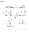
- FIG. 4 is a driving waveform diagram illustrating the operation of a plasma display apparatus according to the first embodiment of the present invention.
- FIG. 5 illustrates a second embodiment of a plasma display apparatus according to the present invention.
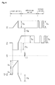
- FIG. 6 is a driving waveform diagram illustrating the operation of a plasma display apparatus according to the second embodiment of the present invention.
- FIG. 7 illustrates a third embodiment of a plasma display apparatus according to the present invention.
- FIG. 8 is a driving waveform diagram illustrating the operation of a plasma display apparatus according to the third embodiment of the present invention.
- the first ramp-up pulse rises from a ground level to a sustain voltage.
- a driving apparatus of a plasma display panel comprises: a plasma display panel Cp, a first ramp pulse applying unit 300, a voltage applying unit 400, a second ramp pulse applying unit 500, a bias voltage applying unit 600, a scan pulse supplying unit 700, a first sustain pulse supplying unit 800 and a second sustain pulse supplying unit 900.
- the plasma display panel Cp comprises a scan electrode Y and a sustain electrode Z.
- the first ramp pulse applying unit 300 applies the first ramp-up pulse rising up to a first setup voltage Vsetup1 to the scan electrode Y.
- the first ramp pulse applying unit 300 applies the first ramp-up pulse, generated by turning-on a tenth switch S10 that is the first setup switch operating in an active region, to the scan electrode Y.
- the voltage applying unit 400 applies a first negative voltage V1 to the sustain electrode while the first ramp-up pulse is applied to the scan electrode Y.
- the voltage applying unit 400 applies the first negative voltage V1 to the sustain electrode Z by turning-on of a ninth switch S9 that is the switch for applying voltage.
- the first negative voltage V1 is a negative sustain voltage -Vs.
- the sustain voltage Vs is a voltage for sustaining the sustain discharge of the plasma display panel.
- the second ramp pulse applying unit 500 applies a second ramp-up pulse rising up to a second setup voltage Vsetup2 to the sustain electrode Z, after the first negative voltage V1 is applied. At this time, the second ramp pulse applying unit 500 applies the second ramp-up pulse, generated by turning-on a eleventh switch S11 that is the second setup switch operating in an active region, to the sustain electrode Z.
- the bias voltage applying unit 600 applies a scan bias voltage Vsc to the scan electrode Y in an addressing period, after the second ramp-up pulse is applied by means of the second ramp-pulse applying unit 500.
- the scan pulse supplying unit 700 supplies the voltage -Vw for scan pulse in order to perform an addressing on the cell positioned on the selected scan electrode. At this time, the application of the voltage for scan pulse-Vw is done by turning-on a twelfth switch S12. A data pulse synchronizing with a scan pulse supplied by the scan pulse supplying unit 700 is applied to an address electrode (not shown) and thereby, an addressing is done.
- the first sustain pulse supplying unit 800 supplies the energy stored in a capacitor Csl for recovering and storing energy by using a resonance between a first inductor L1 and a second inductor L2 to the scan electrode Y, and recovers it from the scan electrode Y by using a resonance between the first inductor L1 and the second inductor L2, after an addressing period, thereby supplying a sustain pulse.
- the second sustain pulse supplying unit 900 applies the sustain voltage Vs, i.e., a bias voltage, to the sustain electrode Z, after the second ramp-up pulse is applied by the second ramp pulse applying unit 500, and applies the sustain pulse alternating with the sustain pulse supplied by the first sustain pulse supplying unit 800 to the sustain electrode Z.
- Vs sustain voltage
- the second sustain pulse supplying unit 900 applies the sustain voltage Vs, i.e., a bias voltage, to the sustain electrode Z, after the second ramp-up pulse is applied by the second ramp pulse applying unit 500, and applies the sustain pulse alternating with the sustain pulse supplied by the first sustain pulse supplying unit 800 to the sustain electrode Z.
- the reference numeral 1000 is a scan driver.
- the scan driver 1000 Y turns-on or turns-off a thirteenth switch S13, i.e., a first selection switch, and a fourteenth switch S14, i.e., a second selection switch for applying a driving waveform to the scan electrode.
- FIG. 4 is a driving waveform diagram illustrating the operation of a plasma display apparatus according to the first embodiment of the present invention.
- the voltage applying unit 400 applies a negative sustain voltage - Vs , i.e., a first negative voltage V1, to the sustain electrode Z by turning-on the ninth switch S9 that is the switch for applying voltage.
- the first ramp pulse applying unit 300 applies the first ramp-up pulse rising from a ground level voltage to the first setup voltage Vsetup1 to the scan electrode Y.
- the first ramp pulse applying unit 300 is able to apply the first ramp-up pulse rising from a ground level voltage to the first setup voltage Vsetup1, because the second switch S2 of the first sustain pulse supplying unit 800 is turned-off.
- the potential difference between the scan electrode Y and the sustain electrode Z is the same with the waveform of the driving pulse applied to the scan electrode Y in the setup period of FIG. 2.
- the sixth switch S6 included in the conventional plasma display apparatus is not needed. That is, the sixth switch S6 included in the conventional plasma display apparatus should be a high withstand voltage switch, in order to pass through the setup voltage Vsetup and the sustain voltage Vs.
- the plasma display apparatus of the present invention separates the first ramp-up pulse and the negative sustain voltage -Vs and applies each of them to the scan electrode Y and the sustain electrode Z, respectively, such that any high withstand voltage switch such as the sixth switch S6 is not needed.
- the second ramp pulse applying unit 500 applies the second ramp-up pulse rising up to the second setup voltage Vsetup2 to the sustain electrode Z. Therefore, the potential difference between the scan electrode Y and the sustain electrode Y is the same with the waveform until the ending point of setdown period, as illustrated in FIG. 3.
- the bias voltage applying unit 600 applies the scan bias voltage Vsc to the scan electrode Y in an addressing period.
- the scan pulse supplying unit 700 supplies the voltage for scan pulse -Vw, in order to perform an addressing on the cell on the selected scan line.
- the second sustain pulse supplying unit 900 applies the sustain voltage Vs to the sustain electrode Z through the turned-on sixth switch S6.
- the scan bias voltage Vsc or the voltage for scan pulse -Vw is applied to the scan electrode Y, and the sustain voltage Vs playing a role of a bias voltage is applied to the sustain electrode Z, in an addressing period, as illustrated in FIG. 4.
- the second switch S2 of the first sustain pulse supplying unit 800 becomes a turn-off status. That is, the conventional plasma display apparatus applies the voltage of Vs to the first node n1 and the write scan voltage -Vw to the second node n2 in the setdown period, as illustrated in FIG.1, such that the seventh switch S7 with the characteristic withstanding high voltage is needed.
- the plasma display apparatus of the present invention does not need a high withstand voltage switching element such as the seventh switch S7.
- the eighth switch S8 of the conventional driving apparatus is not needed. Also, as illustrated in FIG. 3, since the scan electrode Y becomes a ground level by the turn-on of the fourth switch S4 and the fourteenth switch S14, the ninth switch S9 of FIG. 1 is not needed.
- a driving apparatus of a plasma display panel comprises: a plasma display panel Cp, a first ramp pulse applying unit 300, a voltage applying unit 400, a second ramp pulse applying unit 500, a bias voltage applying unit 600, a scan pulse supplying unit 700, a first sustain pulse supplying unit 800 and a second sustain pulse supplying unit 900.
- the plasma display panel Cp comprises a scan electrode Y and a sustain electrode Z.
- the first ramp pulse applying unit 300 applies the first ramp-up pulse rising up to a sustain voltage Vs to the scan electrode Y.
- the first ramp pulse applying unit 300 applies the first ramp-up pulse, generated by turning-on a tenth switch S10 that is the first setup switch operating in an active region, to the scan electrode Y. That is, the first ramp pulse applying unit 300 in the first embodiment of the present invention needs a separate first setup voltage source Vsetup1, however, the first ramp pulse applying unit 300 in the second embodiment of the present invention generates the first ramp-up pulse with the sustain voltage Vs without a separate first setup voltage source Vsetup1.
- the voltage applying unit 400 applies a first negative voltage V1 to the sustain electrode while the first ramp-up pulse is applied to the scan electrode Y.
- the voltage applying unit 400 applies the first negative voltage V1 to the sustain electrode Z by turning-on of a ninth switch S9 that is the switch for applying voltage.
- the first negative voltage V1 is a negative Sustain voltage -Vs.
- the sustain voltage Vs is a voltage for sustaining the sustain discharge of the plasma display panel.
- the second ramp pulse applying unit 500 applies a second ramp-up pulse rising up to the sustain voltage Vs to the sustain electrode Z, after the first negative voltage V1 is applied. At this time, the second ramp pulse applying unit 500 applies the second ramp-up pulse, generated by turning-on a eleventh switch S11 that is the second setup switch operating in an active region, to the sustain electrode Z. That is, the first ramp pulse applying unit 300 in the first embodiment of the present invention needs a separate second setup voltage source Vsetup2, however, the second ramp pulse applying unit 500 in the second embodiment of the present invention generates the second ramp-up pulse with the sustain voltage Vs without a separate second setup voltage source Vsetup2.
- the bias voltage applying unit 600 applies a ground level voltage to the scan electrode Y in an addressing period, after the second ramp-up pulse is applied by means of the second ramp-pulse applying unit 500. Therefore, a separate scan bias voltage source Vsc as in the first embodiment of the present invention is not needed.
- the scan pulse supplying unit 700 supplies the voltage -Vw for scan pulse in order to perform an addressing on the cell positioned on the selected scan electrode. At this time, the application of the voltage for scan pulse-Vw is done by turning-on a twelfth switch S12. A data pulse synchronizing with a scan pulse supplied by the scan pulse supplying unit 700 is applied to an address electrode (not shown) and thereby, an addressing is done.
- the first sustain pulse supplying unit 800 supplies the energy stored in a capacitor Csl for recovering and storing energy by using a resonance between a first inductor L1 and a second inductor L2 to the scan electrode Y, and recovers it from the scan electrode Y by using a resonance between the first inductor L1 and the second inductor L2, after an addressing period, thereby supplying a sustain pulse.
- the second sustain pulse supplying unit 900 applies the sustain voltage Vs, i.e., a bias voltage, to the sustain electrode Z, after the second ramp-up pulse is applied by the second ramp pulse applying unit 500, and applies the sustain pulse alternating with the sustain pulse supplied by the first sustain pulse supplying unit 800 to the sustain electrode Z.
- Vs sustain voltage
- the second sustain pulse supplying unit 900 applies the sustain voltage Vs, i.e., a bias voltage, to the sustain electrode Z, after the second ramp-up pulse is applied by the second ramp pulse applying unit 500, and applies the sustain pulse alternating with the sustain pulse supplied by the first sustain pulse supplying unit 800 to the sustain electrode Z.
- the reference numeral 1000 is a scan driver.
- the scan driver 1000 Y turns-on or turns-off a thirteenth switch S13, i.e., a first selection switch, and a fourteenth switch S14, i.e., a second selection switch for applying a driving waveform to the scan electrode.
- the voltage applying unit 400 applies a negative sustain voltage-Vs , i.e., a first negative voltage V1, to the sustain electrode Z by turning-on the ninth switch S9 that is the switch for applying voltage.
- the first ramp pulse applying unit 300 applies the first ramp-up pulse rising up to the sustain voltage Vs to the scan electrode Y.
- the potential difference between the scan electrode Y and the sustain electrode Z rises up to 2Vs in a setup period as illustrated in FIG. 6.
- the sixth switch S6 included in the conventional plasma display apparatus is not needed.
- the second ramp pulse sustain unit 500 applies the second ramp-up pulse rising up to the sustain voltage Vs to the sustain electrode Z. Therefore, the potential difference between the scan electrode Y and the sustain electrode Y falls up to the negative sustain voltage -Vs in the setup period.
- the bias voltage applying unit 600 applies the ground level voltage to the scan electrode Y in an addressing period.
- the scan pulse supplying unit 700 supplies the voltage for scan pulse -Vw, in order to perform an addressing on the cell on the selected scan line.
- the second sustain pulse supplying unit 900 applies the sustain voltage Vs to the sustain electrode Z through the turned-on sixth switch S6.
- the ground level voltage Vsc or the voltage for scan pulse - Vw is applied to the scan electrode Y, and the sustain voltage Vs playing a role of a bias voltage is applied to the sustain electrode Z, in an addressing period, as illustrated in FIG. 4,
- the plasma display apparatus of the present invention does not need a high withstand voltage switching element such as the seventh switch S7, unlike the plasma display apparatus of the conventional plasma display apparatus.
- the eighth switch S8 of the conventional driving apparatus is not needed. Also, as illustrated in FIG. 3, since the scan electrode Y becomes a ground level by the turn-on of the fourth switch S4 and the fourteenth switch S14, the ninth switch S9 of FIG. 1 is not needed.
- the difference between the second embodiment and the third embodiment of the present invention illustrated in FIGS. 7 and 8 is that the eleventh switch S11 of the second ramp pulse applying unit 500 is connected in parallel to the eighth switch S8 of the second sustain pulse supplying unit 900.
- the eleventh switch S11 of the second ramp waveform supplying unit 350 is connected in parallel to the eighth switch S8, as illustrated in FIG. 8, after the negative sustain voltage -Vs is applied to the sustain electrode Y, the eleventh switch generates the second ramp-up pulse with being turned-on. At this time, the potential of the sustain electrode Y rises from the negative sustain voltage -Vs to the ground. Thereafter, the seventh switch S7 turns-on so that the sustain voltage Vs is applied to the sustain electrode Z.
- the potential difference between the scan electrode Y and the sustain electrode Z rises up to the 2Vs in the setup period, and falls up to the ground level in the setdown period.
Landscapes
- Engineering & Computer Science (AREA)
- Physics & Mathematics (AREA)
- Power Engineering (AREA)
- Plasma & Fusion (AREA)
- Computer Hardware Design (AREA)
- General Physics & Mathematics (AREA)
- Theoretical Computer Science (AREA)
- Control Of Indicators Other Than Cathode Ray Tubes (AREA)
- Control Of Gas Discharge Display Tubes (AREA)
Abstract
Description
- The present invention relates to a plasma display apparatus and driving method thereof. It more specifically to a plasma display apparatus and driving method thereof to perform a reset driving.
- FIG. 1 is a circuit diagram of a plasma display apparatus of the prior art. FIG. 2 is a driving waveform diagram according to the operation of a plasma display apparatus of the prior art.
- A fifth switch S5 and a seventh switch S7 are turned-on during a setup period. At this time, a sustain voltage Vs is supplied from a sustain
pulse supplying unit 40. The sustain voltage supplied from the sustainpulse supplying unit 40 is supplied to scan electrodes via an internal diode of a sixth switch Q6, the seventh switch Q7 and a second selecting unit Q15 of a drive integrated circuit 52. Therefore, as illustrated in FIG. 2, the voltage of the scan electrodes Y is rapidly risen to Vs. - Meanwhile, since the sustain voltage Vs is supplied to a negative polarity terminal of a second capacitor C2, the second capacitor C2 supplies the voltage of Vs+Vsetup to the fifth switch Q5. The fifth switch Q5 supplies the voltage supplied from the second capacitor C2 to a first node point n1 with a predetermined gradient, while the channel width thereof is controlled by a first variable resistor VR1 positioned in front of the fifth switch.
- The voltage applied to the first node point n1 with a predetermined gradient is supplied to the scan electrodes via the seventh switch Q7 and the second selecting unit Q15 of the drive integrated circuit 52. Through such a process, as illustrated in FIG. 2, a ramp-up pulse is supplied to the scan electrodes Y.
- After the ramp-up pulse is supplied to the scan electrodes Y, the fifth switch Q5 is turned-off. When the fifth switch Q5 is turned-off, only the voltage of the Vs supplied from the sustain
pulse supplying unit 40 is applied to the first node point n1, and accordingly, as illustrated in FIG. 2, the voltage of the scan electrodes Y is rapidly fallen to the Vs. - Thereafter, the seventh switch Q7 is turned-off and at the same time, a tenth switch Q10 is turned-on, during a setdown period. The tenth switch Q10 falls the voltage of a second node n2 to a write scan voltage -Vw (or setdown voltage source) with a predetermined gradient, while the channel width thereof is controlled by a second variable resistor VR2 positioned in front of the tenth switch. Accordingly, as illustrated in FIG.2, the ramp-down pulse is supplied to the scan electrodes Y and the potential of the scan electrodes Y falls to the -Vw.
- Here, the seventh switch Q7 comprises the internal diode having a different direction from the sixth switch Q6, and thereby, prevents the voltage applied to the second node n2 from being supplied to a ground potential GND via the internal diode of the sixth switch Q6 and the internal diode of the fourth switch Q4.
- The scan standard
voltage supplying unit 50 comprises a third capacitor C3 connected between a scan bias voltage source Vsc and the second node n2, and an eighth switch Q8 and a ninth switch Q9 connected between the scan bias voltage source Vsc and the second node n2. - The eighth switch Q8, supplies the voltage of the scan bias voltage source Vsc to the drive integrated circuit 52, while being switched over by a control signal supplied from a timing controller during a selective write and erasing address, as illustrated in FIG. 2. The third capacitor C3 adds the voltage applied to the second node n2 and the voltage value of the scan bias voltage source Vsc to supply it to the eight switch Q8. The ninth switch Q9 is turned-on together with a fourteenth switch Q14, the seventh switch Q7, the sixth switch Q6 and the fourth switch Q4, such that the potential of the scan electrode Y becomes a ground level.
- In the driving apparatus of the plasma display panel of the prior art operating as above, since the voltage size (Vsetup+Vs), at which a ramp-up waveform arrives, is large and the rising time thereof is long, the current flowing into the fifth switch Q5 is gradually increased and thus, high heat is generated. Therefore, the fifth switch Q5 must withstand a high voltage and a high current.
- Therefore, since the fifth switch Q5 is a high expensive switching element with a very superior performance, the manufacturing cost of the plasma display panel is increased. Also, due to noise generated in response to the operation of the fifth switch Q5, peripheral switch elements adjacent thereto suffer from bad influences.
- Accordingly, in order to isolate the fifth switch Q5 and the switches adjacent thereto, the sixth switch Q6 and the seventh switch Q7 should be provided separately.
- In particular, when the ramp-up pulse is supplied, since the sixth switch is turned-off and the sustain voltage Vs is thereby applied through the internal diode of the sixth switch Q6, the sixth switch Q6 isolates an
energy recovery circuit 40 and asetup supplying unit 42. - At this time, since the setup voltage Vsetup and the sustain voltage Vs pass through the sixth switch Q6, the sixth switch Q6 should be a high withstand voltage switch withstanding voltage higher than the setup voltage applying a setup waveform, resulting in the problems that the manufacturing cost of the plasma display panel is increased and energy loss is significantly occurred.
- Also, the seventh switch Q7 comprises the internal diode having a different direction from the sixth switch Q6, and thereby, prevents the voltage applied to the second node n2 from being supplied to a ground potential GND via the internal diode of the sixth switch Q6 and the internal diode of the fourth switch Q4. During a setdown period, the voltage of the Vs is applied to the first node n1 and the write scan voltage -Vw is applied to the second node n2. Here, if the voltage of the Vs is set up as about 180V and the write scan voltage -Vw is set up as about -70V, the seventh switch Q7 should have an withstand voltage on the order of about 250V (300V in consideration of a substantial driving voltage margin). That is, in the prior art, the seventh switch Q7 should be provided with a switching elements having a high withstand voltage, resulting in a problem that the manufacturing cost of the plasma display panel is increased.
- In addition, it has further caused the problem that the conventional driving apparatus needs a separate setup voltage source Vsetup for forming the ramp-up waveform.
- The present invention is to solve at least the problems and disadvantages of the background art.
- The present invention seeks to provide an improved plasma display apparatus and a driving method thereof.
- A plasma display apparatus according to the present invention comprises: a plasma display panel comprising a scan electrode and a sustain electrode; a first ramp pulse applying unit applying a first ramp-up pulse to the scan electrode; a voltage applying unit applying a first negative voltage to the sustain electrode while the first ramp-up pulse is applied to the scan electrode; and a second ramp pulse applying unit applying a second ramp-up pulse to the sustain electrode after the first negative voltage is applied.
- A driving method of a plasma display apparatus according to the present invention comprises the steps of: applying the first ramp-up pulse to the first scan electrode; applying the first negative voltage to the sustain electrode while the first ramp-up pulse is applied to the scan electrode; and applying the second ramp-up pulse to the sustain electrode, after the first negative voltage is applied.
- Embodiments of the present invention allow the driving voltage applied to the scan electrode to be lowered by applying a driving pulse to the scan electrode and the sustain electrode in a setup period and a setdown period.
- Embodiments of the invention will be described with reference to the drawings in which like numerals refer to like elements.
- FIG. 1 is a circuit diagram illustrating a plasma display apparatus of the
- FIG. 2 illustrates a driving waveform diagram according to the operation of a plasma display apparatus of the prior art.
- FIG. 3 illustrates a first embodiment of a plasma display apparatus according to the present invention.
- FIG. 4 is a driving waveform diagram illustrating the operation of a plasma display apparatus according to the first embodiment of the present invention.
- FIG. 5 illustrates a second embodiment of a plasma display apparatus according to the present invention.
- FIG. 6 is a driving waveform diagram illustrating the operation of a plasma display apparatus according to the second embodiment of the present invention.
- FIG. 7 illustrates a third embodiment of a plasma display apparatus according to the present invention.
- FIG. 8 is a driving waveform diagram illustrating the operation of a plasma display apparatus according to the third embodiment of the present invention.
- The first ramp-up pulse rises from a ground level to a sustain voltage.
- As illustrated in FIG. 3, a driving apparatus of a plasma display panel according to the first embodiment comprises: a plasma display panel Cp, a first ramp
pulse applying unit 300, avoltage applying unit 400, a second ramppulse applying unit 500, a biasvoltage applying unit 600, a scanpulse supplying unit 700, a first sustainpulse supplying unit 800 and a second sustainpulse supplying unit 900. - The plasma display panel Cp comprises a scan electrode Y and a sustain electrode Z.
- The first ramp
pulse applying unit 300 applies the first ramp-up pulse rising up to a first setup voltage Vsetup1 to the scan electrode Y. The first ramppulse applying unit 300 applies the first ramp-up pulse, generated by turning-on a tenth switch S10 that is the first setup switch operating in an active region, to the scan electrode Y. - The
voltage applying unit 400 applies a first negative voltage V1 to the sustain electrode while the first ramp-up pulse is applied to the scan electrode Y. Thevoltage applying unit 400 applies the first negative voltage V1 to the sustain electrode Z by turning-on of a ninth switch S9 that is the switch for applying voltage. At this time, preferably, the first negative voltage V1 is a negative sustain voltage -Vs. The sustain voltage Vs is a voltage for sustaining the sustain discharge of the plasma display panel. - The second ramp
pulse applying unit 500 applies a second ramp-up pulse rising up to a second setup voltage Vsetup2 to the sustain electrode Z, after the first negative voltage V1 is applied. At this time, the second ramppulse applying unit 500 applies the second ramp-up pulse, generated by turning-on a eleventh switch S11 that is the second setup switch operating in an active region, to the sustain electrode Z. - The bias
voltage applying unit 600 applies a scan bias voltage Vsc to the scan electrode Y in an addressing period, after the second ramp-up pulse is applied by means of the second ramp-pulse applying unit 500. - The scan
pulse supplying unit 700 supplies the voltage -Vw for scan pulse in order to perform an addressing on the cell positioned on the selected scan electrode. At this time, the application of the voltage for scan pulse-Vw is done by turning-on a twelfth switch S12. A data pulse synchronizing with a scan pulse supplied by the scanpulse supplying unit 700 is applied to an address electrode (not shown) and thereby, an addressing is done. - The first sustain
pulse supplying unit 800 supplies the energy stored in a capacitor Csl for recovering and storing energy by using a resonance between a first inductor L1 and a second inductor L2 to the scan electrode Y, and recovers it from the scan electrode Y by using a resonance between the first inductor L1 and the second inductor L2, after an addressing period, thereby supplying a sustain pulse. - The second sustain
pulse supplying unit 900 applies the sustain voltage Vs, i.e., a bias voltage, to the sustain electrode Z, after the second ramp-up pulse is applied by the second ramppulse applying unit 500, and applies the sustain pulse alternating with the sustain pulse supplied by the first sustainpulse supplying unit 800 to the sustain electrode Z. - The
reference numeral 1000 is a scan driver. The scan driver 1000 Y turns-on or turns-off a thirteenth switch S13, i.e., a first selection switch, and a fourteenth switch S14, i.e., a second selection switch for applying a driving waveform to the scan electrode. - The operation associated with a driving apparatus of a plasma display penal according to the present invention will be described below in detail with reference to the drawing.
- FIG. 4 is a driving waveform diagram illustrating the operation of a plasma display apparatus according to the first embodiment of the present invention.
- First, the
voltage applying unit 400 applies a negative sustain voltage - Vs , i.e., a first negative voltage V1, to the sustain electrode Z by turning-on the ninth switch S9 that is the switch for applying voltage. At the same time, the first ramppulse applying unit 300 applies the first ramp-up pulse rising from a ground level voltage to the first setup voltage Vsetup1 to the scan electrode Y. The first ramppulse applying unit 300 is able to apply the first ramp-up pulse rising from a ground level voltage to the first setup voltage Vsetup1, because the second switch S2 of the first sustainpulse supplying unit 800 is turned-off. - As above, by simultaneously applying the first ramp-up pulse and the negative sustain voltage -Vs to the scan electrode Y, the potential difference between the scan electrode Y and the sustain electrode Z is the same with the waveform of the driving pulse applied to the scan electrode Y in the setup period of FIG. 2.
- As above, by applying each of the first ramp-up pulse and the negative sustain voltage -Vs to the scan electrode Y and the sustain electrode Z, respectively, the sixth switch S6 included in the conventional plasma display apparatus is not needed. That is, the sixth switch S6 included in the conventional plasma display apparatus should be a high withstand voltage switch, in order to pass through the setup voltage Vsetup and the sustain voltage Vs. However, the plasma display apparatus of the present invention separates the first ramp-up pulse and the negative sustain voltage -Vs and applies each of them to the scan electrode Y and the sustain electrode Z, respectively, such that any high withstand voltage switch such as the sixth switch S6 is not needed.
- Thereafter, the second ramp
pulse applying unit 500 applies the second ramp-up pulse rising up to the second setup voltage Vsetup2 to the sustain electrode Z. Therefore, the potential difference between the scan electrode Y and the sustain electrode Y is the same with the waveform until the ending point of setdown period, as illustrated in FIG. 3. - Next, the bias
voltage applying unit 600 applies the scan bias voltage Vsc to the scan electrode Y in an addressing period. In addition, the scanpulse supplying unit 700 supplies the voltage for scan pulse -Vw, in order to perform an addressing on the cell on the selected scan line. And, the second sustainpulse supplying unit 900 applies the sustain voltage Vs to the sustain electrode Z through the turned-on sixth switch S6. - Accordingly, the scan bias voltage Vsc or the voltage for scan pulse -Vw is applied to the scan electrode Y, and the sustain voltage Vs playing a role of a bias voltage is applied to the sustain electrode Z, in an addressing period, as illustrated in FIG. 4.
- When the voltage for scan pulse -Vw is applied as above, the second switch S2 of the first sustain
pulse supplying unit 800 becomes a turn-off status. That is, the conventional plasma display apparatus applies the voltage of Vs to the first node n1 and the write scan voltage -Vw to the second node n2 in the setdown period, as illustrated in FIG.1, such that the seventh switch S7 with the characteristic withstanding high voltage is needed. However, the plasma display apparatus of the present invention does not need a high withstand voltage switching element such as the seventh switch S7. - Also, since the scan bias voltage Vsc is applied to the scan electrode Y through the thirteenth switch S13 of the
scan driver 1000, the eighth switch S8 of the conventional driving apparatus, as illustrated in FIG. 1, is not needed. Also, as illustrated in FIG. 3, since the scan electrode Y becomes a ground level by the turn-on of the fourth switch S4 and the fourteenth switch S14, the ninth switch S9 of FIG. 1 is not needed. - As illustrated in FIG. 5, a driving apparatus of a plasma display panel comprises: a plasma display panel Cp, a first ramp
pulse applying unit 300, avoltage applying unit 400, a second ramppulse applying unit 500, a biasvoltage applying unit 600, a scanpulse supplying unit 700, a first sustainpulse supplying unit 800 and a second sustainpulse supplying unit 900. - The plasma display panel Cp comprises a scan electrode Y and a sustain electrode Z.
- The first ramp
pulse applying unit 300 applies the first ramp-up pulse rising up to a sustain voltage Vs to the scan electrode Y. The first ramppulse applying unit 300 applies the first ramp-up pulse, generated by turning-on a tenth switch S10 that is the first setup switch operating in an active region, to the scan electrode Y. That is, the first ramppulse applying unit 300 in the first embodiment of the present invention needs a separate first setup voltage source Vsetup1, however, the first ramppulse applying unit 300 in the second embodiment of the present invention generates the first ramp-up pulse with the sustain voltage Vs without a separate first setup voltage source Vsetup1. - The
voltage applying unit 400 applies a first negative voltage V1 to the sustain electrode while the first ramp-up pulse is applied to the scan electrode Y. Thevoltage applying unit 400 applies the first negative voltage V1 to the sustain electrode Z by turning-on of a ninth switch S9 that is the switch for applying voltage. At this time, preferably, the first negative voltage V1 is a negative Sustain voltage -Vs. The sustain voltage Vs is a voltage for sustaining the sustain discharge of the plasma display panel. - The second ramp
pulse applying unit 500 applies a second ramp-up pulse rising up to the sustain voltage Vs to the sustain electrode Z, after the first negative voltage V1 is applied. At this time, the second ramppulse applying unit 500 applies the second ramp-up pulse, generated by turning-on a eleventh switch S11 that is the second setup switch operating in an active region, to the sustain electrode Z. That is, the first ramppulse applying unit 300 in the first embodiment of the present invention needs a separate second setup voltage source Vsetup2, however, the second ramppulse applying unit 500 in the second embodiment of the present invention generates the second ramp-up pulse with the sustain voltage Vs without a separate second setup voltage source Vsetup2. - The bias
voltage applying unit 600 applies a ground level voltage to the scan electrode Y in an addressing period, after the second ramp-up pulse is applied by means of the second ramp-pulse applying unit 500. Therefore, a separate scan bias voltage source Vsc as in the first embodiment of the present invention is not needed. - The scan
pulse supplying unit 700 supplies the voltage -Vw for scan pulse in order to perform an addressing on the cell positioned on the selected scan electrode. At this time, the application of the voltage for scan pulse-Vw is done by turning-on a twelfth switch S12. A data pulse synchronizing with a scan pulse supplied by the scanpulse supplying unit 700 is applied to an address electrode (not shown) and thereby, an addressing is done. - The first sustain
pulse supplying unit 800 supplies the energy stored in a capacitor Csl for recovering and storing energy by using a resonance between a first inductor L1 and a second inductor L2 to the scan electrode Y, and recovers it from the scan electrode Y by using a resonance between the first inductor L1 and the second inductor L2, after an addressing period, thereby supplying a sustain pulse. - The second sustain
pulse supplying unit 900 applies the sustain voltage Vs, i.e., a bias voltage, to the sustain electrode Z, after the second ramp-up pulse is applied by the second ramppulse applying unit 500, and applies the sustain pulse alternating with the sustain pulse supplied by the first sustainpulse supplying unit 800 to the sustain electrode Z. - The
reference numeral 1000 is a scan driver. The scan driver 1000 Y turns-on or turns-off a thirteenth switch S13, i.e., a first selection switch, and a fourteenth switch S14, i.e., a second selection switch for applying a driving waveform to the scan electrode. - The operation associated with a driving apparatus of a plasma display penal according to the present invention will be described below in detail with reference to FIG. 6.
- First, the
voltage applying unit 400 applies a negative sustain voltage-Vs , i.e., a first negative voltage V1, to the sustain electrode Z by turning-on the ninth switch S9 that is the switch for applying voltage. At the same time, the first ramppulse applying unit 300 applies the first ramp-up pulse rising up to the sustain voltage Vs to the scan electrode Y. - As above, by simultaneously applying the first ramp-up pulse and the negative sustain voltage -Vs to the scan electrode Y, the potential difference between the scan electrode Y and the sustain electrode Z rises up to 2Vs in a setup period as illustrated in FIG. 6.
- As above, by applying each of the first ramp-up pulse and the negative sustain voltage -Vs to the scan electrode Y and the sustain electrode Z, respectively, the sixth switch S6 included in the conventional plasma display apparatus is not needed.
- Thereafter, the second ramp pulse sustain
unit 500 applies the second ramp-up pulse rising up to the sustain voltage Vs to the sustain electrode Z. Therefore, the potential difference between the scan electrode Y and the sustain electrode Y falls up to the negative sustain voltage -Vs in the setup period. - Next, the bias
voltage applying unit 600 applies the ground level voltage to the scan electrode Y in an addressing period. In addition, the scanpulse supplying unit 700 supplies the voltage for scan pulse -Vw, in order to perform an addressing on the cell on the selected scan line. And, the second sustainpulse supplying unit 900 applies the sustain voltage Vs to the sustain electrode Z through the turned-on sixth switch S6. - Accordingly, the ground level voltage Vsc or the voltage for scan pulse - Vw is applied to the scan electrode Y, and the sustain voltage Vs playing a role of a bias voltage is applied to the sustain electrode Z, in an addressing period, as illustrated in FIG. 4,
- When the voltage for scan pulse -Vw is applied as above, the second switch S2 of the first sustain
pulse supplying unit 800 becomes a turn-off status. Therefore, the plasma display apparatus of the present invention does not need a high withstand voltage switching element such as the seventh switch S7, unlike the plasma display apparatus of the conventional plasma display apparatus. - Also, since the ground level voltage is applied to the scan electrode Y through the thirteenth switch S13 of the
scan driver 1000, the eighth switch S8 of the conventional driving apparatus, as illustrated in FIG. 1, is not needed. Also, as illustrated in FIG. 3, since the scan electrode Y becomes a ground level by the turn-on of the fourth switch S4 and the fourteenth switch S14, the ninth switch S9 of FIG. 1 is not needed. - The difference between the second embodiment and the third embodiment of the present invention illustrated in FIGS. 7 and 8 is that the eleventh switch S11 of the second ramp
pulse applying unit 500 is connected in parallel to the eighth switch S8 of the second sustainpulse supplying unit 900. - If the eleventh switch S11 of the second ramp waveform supplying unit 350 is connected in parallel to the eighth switch S8, as illustrated in FIG. 8, after the negative sustain voltage -Vs is applied to the sustain electrode Y, the eleventh switch generates the second ramp-up pulse with being turned-on. At this time, the potential of the sustain electrode Y rises from the negative sustain voltage -Vs to the ground. Thereafter, the seventh switch S7 turns-on so that the sustain voltage Vs is applied to the sustain electrode Z.
- Accordingly, the potential difference between the scan electrode Y and the sustain electrode Z rises up to the 2Vs in the setup period, and falls up to the ground level in the setdown period.
- The invention being thus described, it will be obvious that the same may be varied in may ways. Such variations are not to be regarded as departure from the scope of the invention, and all such modifications as would be obvious to one skilled in the art intended to be included within the scope of the following claims.
Claims (20)
- A plasma display apparatus comprising:a plasma display panel comprising a scan electrode and a sustain electrode;a first ramp pulse applying unit arranged to apply a first ramp-up pulse to the scan electrode;a voltage applying unit arranged to apply a first negative voltage to the sustain electrode while the first ramp-up pulse is applied to the scan electrode; anda second ramp pulse applying unit arranged to apply a second ramp-up pulse to the sustain electrode after the first negative voltage is applied.
- The plasma display apparatus of claim 1, wherein the first ramp pulse applying unit comprises means for applying a first ramp-up pulse rising from a ground level voltage to a first setup voltage to the scan electrode.
- The plasma display apparatus of claim 2, the first ramp pulse applying unit comprises a first setup switch, arranged to generate the first ramp-up pulse by the first setup voltage applied to one terminal thereof and to apply the first ramp-up pulse to the scan electrode through other terminal thereof.
- The plasma display apparatus of claim 1, wherein the first ramp pulse applying unit comprises means to apply the first ramp-up pulse rising from a ground level voltage to a sustain voltage to the scan electrode.
- The plasma display apparatus of claim 4, wherein the first ramp pulse applying unit comprises a first setup switch, arranged to generate the first ramp-up pulse by the sustain voltage applied to one terminal thereof and to apply the first ramp-up pulse to the scan electrode through other terminal thereof.
- The plasma display apparatus of claim 1, wherein the second ramp pulse applying unit comprises means to apply a second ramp-up pulse rising from a ground level voltage to a second setup voltage to the sustain electrode.
- The plasma display apparatus of claim 6, wherein the second ramp pulse applying unit comprises a second setup switch, arranged to generate the second ramp-up pulse by the second setup voltage applied to one terminal thereof and to apply the second ramp-up pulse to the sustain electrode through other terminal thereof.
- The plasma display apparatus of claim 1, wherein the second ramp pulse applying unit comprises means to apply the second ramp-up pulse rising from a ground level voltage to a sustain voltage to the sustain electrode.
- The plasma display apparatus of claim 8, wherein the second ramp pulse applying unit comprises a second setup switch, arranged to generate the second ramp-up pulse by the second sustain voltage applied to one terminal thereof and to apply the second ramp-up pulse to the sustain electrode through other terminal thereof.
- The plasma display apparatus of claim 1, wherein the second ramp pulse applying unit comprises a bias voltage applying unit comprises means to apply a ground level voltage to the scan electrode, after applying the second ramp-up pulse.
- The plasma display apparatus of claim 1, further comprising a sustain pulse supplying unit comprises means for apply a sustain pulse to the sustain electrode; and,
the second ramp pulse applying unit arranged to apply the second ramp-up pulse when the sustain pulse supplying unit recovers energy from the sustain electrode. - The plasma display apparatus of claim 11, wherein the second ramp pulse applying unit comprises a second setup switch arranged to be turned-on upon recovering the energy, by connecting one terminal thereof to the sustain electrode and the other terminal thereof to the ground, and wherein the second ramp pulse applying unit comprises a second setup switch arranged to be turned-on, when the energy is recovered, by one end being connected to the sustain electrode and another end being connected to the ground.
- The plasma display apparatus of claim 3, comprising means to operate the first setup switch in an active region.
- The plasma display apparatus of claim 7, comprising means to operate the second setup switch in an active region.
- A driving method of a plasma display apparatus including the steps of:applying a first ramp-up pulse to a first scan electrode;applying a first negative voltage to a sustain electrode while the first ramp-up pulse is applied to the scan electrode; and,applying a second ramp-up pulse to the sustain electrode after the first negative voltage is applied.
- The driving method of a plasma display apparatus of claim 15, wherein the first ramp-up pulse rises from a ground level to a first setup voltage.
- The driving method of a plasma display apparatus of claim 15, wherein the first ramp-up pulse rises from a ground level to a sustain voltage.
- The driving method of a plasma display apparatus of claim 15, wherein the second ramp-up pulse rises from a ground level to a second setup voltage.
- The driving method of a plasma display apparatus of claim 15, wherein the second ramp-up pulse rises from a negative sustain voltage to a ground level.
- The driving method of a plasma display apparatus of claim 15, further including the step of applying a ground level voltage to the scan electrode after applying the second ramp-up pulse.
Applications Claiming Priority (1)
| Application Number | Priority Date | Filing Date | Title |
|---|---|---|---|
| KR1020040071474A KR20060022602A (en) | 2004-09-07 | 2004-09-07 | Driving apparatus and driving method of plasma display panel |
Publications (2)
| Publication Number | Publication Date |
|---|---|
| EP1635319A2 true EP1635319A2 (en) | 2006-03-15 |
| EP1635319A3 EP1635319A3 (en) | 2006-12-06 |
Family
ID=36158547
Family Applications (1)
| Application Number | Title | Priority Date | Filing Date |
|---|---|---|---|
| EP05255451A Withdrawn EP1635319A3 (en) | 2004-09-07 | 2005-09-06 | Plasma display apparatus and driving method thereof |
Country Status (5)
| Country | Link |
|---|---|
| US (1) | US20060050020A1 (en) |
| EP (1) | EP1635319A3 (en) |
| JP (1) | JP2006079088A (en) |
| KR (1) | KR20060022602A (en) |
| CN (1) | CN1755772A (en) |
Cited By (1)
| Publication number | Priority date | Publication date | Assignee | Title |
|---|---|---|---|---|
| EP1914707A2 (en) | 2006-10-17 | 2008-04-23 | Samsung SDI Co., Ltd. | Driving circuit for a plasma display device |
Families Citing this family (5)
| Publication number | Priority date | Publication date | Assignee | Title |
|---|---|---|---|---|
| KR100867598B1 (en) * | 2006-03-14 | 2008-11-10 | 엘지전자 주식회사 | Plasma Display Panel And Driving Method thereof |
| KR100764665B1 (en) * | 2006-05-22 | 2007-10-08 | 엘지전자 주식회사 | Plasma Display Device and Driving Method |
| KR100898289B1 (en) * | 2007-11-01 | 2009-05-18 | 삼성에스디아이 주식회사 | Plasma display device and driving method thereof |
| KR20090050690A (en) * | 2007-11-16 | 2009-05-20 | 삼성에스디아이 주식회사 | Plasma Display and Driving Device |
| KR101985958B1 (en) | 2017-09-12 | 2019-06-04 | 화일산기(주) | Belt cleaner apparatus with position change function |
Family Cites Families (11)
| Publication number | Priority date | Publication date | Assignee | Title |
|---|---|---|---|---|
| JP3271598B2 (en) * | 1999-01-22 | 2002-04-02 | 日本電気株式会社 | Driving method of AC plasma display and AC plasma display |
| JP3455141B2 (en) * | 1999-06-29 | 2003-10-14 | 富士通株式会社 | Driving method of plasma display panel |
| JP2002072957A (en) * | 2000-08-24 | 2002-03-12 | Matsushita Electric Ind Co Ltd | Driving method of plasma display panel |
| JP2002132208A (en) * | 2000-10-27 | 2002-05-09 | Fujitsu Ltd | Driving method and driving circuit for plasma display panel |
| JP4606612B2 (en) * | 2001-02-05 | 2011-01-05 | 日立プラズマディスプレイ株式会社 | Driving method of plasma display panel |
| JP4512971B2 (en) * | 2001-03-02 | 2010-07-28 | 株式会社日立プラズマパテントライセンシング | Display drive device |
| JP2003330411A (en) * | 2002-05-03 | 2003-11-19 | Lg Electronics Inc | Method and device for driving plasma display panel |
| JP4557201B2 (en) * | 2002-08-13 | 2010-10-06 | 株式会社日立プラズマパテントライセンシング | Driving method of plasma display panel |
| JP2004170587A (en) * | 2002-11-19 | 2004-06-17 | Matsushita Electric Ind Co Ltd | Driving method of plasma display panel |
| JP2004191530A (en) * | 2002-12-10 | 2004-07-08 | Nec Plasma Display Corp | Plasma display panel driving method |
| JP2005292451A (en) * | 2004-03-31 | 2005-10-20 | Fujitsu Hitachi Plasma Display Ltd | Plasma display apparatus and driving method for the same |
-
2004
- 2004-09-07 KR KR1020040071474A patent/KR20060022602A/en not_active Withdrawn
-
2005
- 2005-09-06 EP EP05255451A patent/EP1635319A3/en not_active Withdrawn
- 2005-09-06 US US11/218,563 patent/US20060050020A1/en not_active Abandoned
- 2005-09-07 JP JP2005259276A patent/JP2006079088A/en active Pending
- 2005-09-07 CN CNA2005101037199A patent/CN1755772A/en active Pending
Cited By (2)
| Publication number | Priority date | Publication date | Assignee | Title |
|---|---|---|---|---|
| EP1914707A2 (en) | 2006-10-17 | 2008-04-23 | Samsung SDI Co., Ltd. | Driving circuit for a plasma display device |
| EP1914707A3 (en) * | 2006-10-17 | 2008-10-15 | Samsung SDI Co., Ltd. | Driving circuit for a plasma display device |
Also Published As
| Publication number | Publication date |
|---|---|
| KR20060022602A (en) | 2006-03-10 |
| US20060050020A1 (en) | 2006-03-09 |
| EP1635319A3 (en) | 2006-12-06 |
| JP2006079088A (en) | 2006-03-23 |
| CN1755772A (en) | 2006-04-05 |
Similar Documents
| Publication | Publication Date | Title |
|---|---|---|
| JPH11282416A (en) | Driving circuit for plasma display panel, driving method thereof, and plasma display panel device | |
| JP2001272945A (en) | Driving method for plasma display panel | |
| JP3269451B2 (en) | Display device drive circuit | |
| EP1635319A2 (en) | Plasma display apparatus and driving method thereof | |
| KR100589882B1 (en) | How to drive the display panel | |
| JP2005128530A (en) | Apparatus for energy recovery of plasma display panel | |
| JP4841824B2 (en) | Driving device for plasma display panel | |
| CN100504990C (en) | Method for generating pulses of short duration and device for implementing the method | |
| JP2003233343A (en) | Display panel driving circuit | |
| KR100502348B1 (en) | Energy recovery circuit for address driver of plasma display panel | |
| JP4845355B2 (en) | Method for generating an address signal in a plasma panel and apparatus for realizing the method | |
| KR100625543B1 (en) | Driving device of plasma display panel driven by low reset voltage | |
| KR100647580B1 (en) | Power recovery device of plasma display panel and driving device of plasma display panel | |
| JP3498735B2 (en) | Flat panel display and driving method thereof | |
| JP2007057737A (en) | Plasma display panel driving circuit and plasma display device | |
| JP3475946B2 (en) | Display device, its driving circuit and its driving method | |
| EP1780691A1 (en) | Driving apparatus and method for a plasma display panel | |
| JP4883092B2 (en) | Plasma display device | |
| KR100764662B1 (en) | Plasma display device and driving method thereof | |
| KR100646241B1 (en) | Plasma Display Panel Driving Device | |
| KR100811041B1 (en) | Plasma Display Panel Driving Device | |
| KR100515842B1 (en) | Address driving circuit of display panel and driving method using the same | |
| KR20060004395A (en) | Plasma Display Panel Driver | |
| KR20070017706A (en) | Plasma display device | |
| KR100649526B1 (en) | Plasma display device and driving method thereof |
Legal Events
| Date | Code | Title | Description |
|---|---|---|---|
| PUAI | Public reference made under article 153(3) epc to a published international application that has entered the european phase |
Free format text: ORIGINAL CODE: 0009012 |
|
| 17P | Request for examination filed |
Effective date: 20050922 |
|
| AK | Designated contracting states |
Kind code of ref document: A2 Designated state(s): AT BE BG CH CY CZ DE DK EE ES FI FR GB GR HU IE IS IT LI LT LU LV MC NL PL PT RO SE SI SK TR |
|
| AX | Request for extension of the european patent |
Extension state: AL BA HR MK YU |
|
| PUAL | Search report despatched |
Free format text: ORIGINAL CODE: 0009013 |
|
| RIC1 | Information provided on ipc code assigned before grant |
Ipc: G09G 3/288 20060101AFI20061019BHEP |
|
| AK | Designated contracting states |
Kind code of ref document: A3 Designated state(s): AT BE BG CH CY CZ DE DK EE ES FI FR GB GR HU IE IS IT LI LT LU LV MC NL PL PT RO SE SI SK TR |
|
| AX | Request for extension of the european patent |
Extension state: AL BA HR MK YU |
|
| AKX | Designation fees paid | ||
| RBV | Designated contracting states (corrected) |
Designated state(s): DE FR GB NL |
|
| REG | Reference to a national code |
Ref country code: DE Ref legal event code: 8566 |
|
| 17Q | First examination report despatched |
Effective date: 20071018 |
|
| STAA | Information on the status of an ep patent application or granted ep patent |
Free format text: STATUS: THE APPLICATION IS DEEMED TO BE WITHDRAWN |
|
| 18D | Application deemed to be withdrawn |
Effective date: 20100401 |