EP1633045A1 - Elektrische Schaltung - Google Patents
Elektrische Schaltung Download PDFInfo
- Publication number
- EP1633045A1 EP1633045A1 EP04255320A EP04255320A EP1633045A1 EP 1633045 A1 EP1633045 A1 EP 1633045A1 EP 04255320 A EP04255320 A EP 04255320A EP 04255320 A EP04255320 A EP 04255320A EP 1633045 A1 EP1633045 A1 EP 1633045A1
- Authority
- EP
- European Patent Office
- Prior art keywords
- boolean
- input
- output
- signal
- coupled
- Prior art date
- Legal status (The legal status is an assumption and is not a legal conclusion. Google has not performed a legal analysis and makes no representation as to the accuracy of the status listed.)
- Withdrawn
Links
- 238000010586 diagram Methods 0.000 description 2
- 238000012544 monitoring process Methods 0.000 description 2
- 230000003139 buffering effect Effects 0.000 description 1
- 238000001914 filtration Methods 0.000 description 1
Images

Classifications
-
- H—ELECTRICITY
- H03—ELECTRONIC CIRCUITRY
- H03K—PULSE TECHNIQUE
- H03K7/00—Modulating pulses with a continuously-variable modulating signal
- H03K7/08—Duration or width modulation ; Duty cycle modulation
-
- H—ELECTRICITY
- H03—ELECTRONIC CIRCUITRY
- H03K—PULSE TECHNIQUE
- H03K5/00—Manipulating of pulses not covered by one of the other main groups of this subclass
- H03K5/22—Circuits having more than one input and one output for comparing pulses or pulse trains with each other according to input signal characteristics, e.g. slope, integral
- H03K5/26—Circuits having more than one input and one output for comparing pulses or pulse trains with each other according to input signal characteristics, e.g. slope, integral the characteristic being duration, interval, position, frequency, or sequence
-
- H—ELECTRICITY
- H03—ELECTRONIC CIRCUITRY
- H03K—PULSE TECHNIQUE
- H03K9/00—Demodulating pulses which have been modulated with a continuously-variable signal
- H03K9/08—Demodulating pulses which have been modulated with a continuously-variable signal of duration- or width-mudulated pulses or of duty-cycle modulated pulses
Definitions
- This invention relates to an electrical circuit for use in a drive system involving inverters.
- the feedback signal is derived from the output of the inverter by a circuit using analogue filtering of the pulse width modulated signal output by the inverter in two phases. In this way, the switching frequency is eliminated and the fundamental output voltage frequency derived.
- the resultant analogue signal containing only the fundamental frequency is then typically converted to a digital signal by use of a comparator.
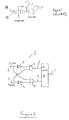
- An example of such a circuit is shown in prior art figure 1.
- a problem with existing circuits is that they have to eliminate a large high frequency signal and to accurately amplify a low frequency signal which has a relatively low amplitude.
- a 5Hz, 5V fundamental frequency may be present on a 750V PWM signal which is a ratio of greater than 150:1).
- very high quality components are required.
- a circuit for providing a signal representative of a fundamental frequency of input PWM signals a first input and a second input to, in use, be coupled to a source of PWM signals means coupled to the inputs to produce a Boolean NOT of the signals, means to produce a Boolean AND of a signal with the Boolean NOT of another to produce a first Boolean output and means to Boolean AND the other signal with the other Boolean NOT to produce a second Boolean output, a set reset latch circuit coupled to the first and the second Boolean outputs and responsive thereto to provide a square wave output at the fundamental frequency of the input PWM signals.
- an electrical circuit 1 in accordance with the invention comprises a first input 2, a second input 3 coupled to an inverter (not shown) producing Pulse Width Modulated (PWM) signals PWMA and PWMB.
- PWM Pulse Width Modulated
- the inputs are connected to a section 4, 5 providing a Boolean NOT operation.
- the sections 4, 5 output PWMA ⁇ and PWMB ⁇ which are coupled to respective Boolean AND sections 6 and 7.
- the other input of the sections 6 and 7 are coupled to the signal inputs 2,3.
- section 6 is connected to input 3 and section 7 is coupled to input 2.
- section 6 has inputs PWMA ⁇ and PWMB and produces the output 8 being PWMA AND PWMB ⁇ .
- Section 7 has inputs PWMB ⁇ and PWMA to produce an output 9 PWMB ⁇ AND PWMA.
- the outputs 8 and 9 are coupled to a Set Reset Latch 10 which produces an output 11 which is the required fundamental frequency of the applied PWM signal.
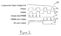
- Figure 3 shows the signals applied to and derived by the circuit 1.
- Signal 30 is the waveform PWMA applied to input 2 and signal 31 is the waveform PWMB applied to input 3. It will be seen that the more positive phase PWMA goes high first and low last. As a result, the logic signal PWMA AND PWMB ⁇ waveform 32 will be low when PWMA is on average more negative than PWMB. When PWMA is more positive, then a train of pulses is produced, the mark space ratio of which is proportional to the average voltage difference between the two phases. A similar signal is derived for PWMA ⁇ AND PWMB as shown in waveform 33.
- waveform 34 is a square waveform matching the fundamental output voltage A-B shown in waveform 35.
- the practical circuit shown in figure 4 uses two transistors 40, 41 to act as two AND gates and inverters. These provide the waveforms 32 and 32 to the set reset latch provided by two AND gates 42 and 43. The resistors are required to correctly bias the transistors.
- the output is labelled 11 as in the figure 3.
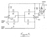
- Figure 5 shows an alternative embodiment using two transistors 40 and 41 to provide the logical gates, inverter and latch. A further transistor 50 to provides buffering for the output 11.
Landscapes
- Physics & Mathematics (AREA)
- Nonlinear Science (AREA)
- Inverter Devices (AREA)
Priority Applications (1)
| Application Number | Priority Date | Filing Date | Title |
|---|---|---|---|
| EP04255320A EP1633045A1 (de) | 2004-09-02 | 2004-09-02 | Elektrische Schaltung |
Applications Claiming Priority (1)
| Application Number | Priority Date | Filing Date | Title |
|---|---|---|---|
| EP04255320A EP1633045A1 (de) | 2004-09-02 | 2004-09-02 | Elektrische Schaltung |
Publications (1)
| Publication Number | Publication Date |
|---|---|
| EP1633045A1 true EP1633045A1 (de) | 2006-03-08 |
Family
ID=34930621
Family Applications (1)
| Application Number | Title | Priority Date | Filing Date |
|---|---|---|---|
| EP04255320A Withdrawn EP1633045A1 (de) | 2004-09-02 | 2004-09-02 | Elektrische Schaltung |
Country Status (1)
| Country | Link |
|---|---|
| EP (1) | EP1633045A1 (de) |
Citations (4)
| Publication number | Priority date | Publication date | Assignee | Title |
|---|---|---|---|---|
| US3313927A (en) * | 1963-10-10 | 1967-04-11 | Gen Electric | Pulse width comparator |
| FR2432798A1 (fr) * | 1978-08-02 | 1980-02-29 | Accumulateurs Fixes | Dispositif de synchronisation antiparasite |
| US5440229A (en) * | 1992-02-18 | 1995-08-08 | Reliance Electric Industrial Company | Fundamental voltmeter |
| EP0730341A2 (de) * | 1995-02-16 | 1996-09-04 | Sony Corporation | Steuergerät für einen Motor |
-
2004
- 2004-09-02 EP EP04255320A patent/EP1633045A1/de not_active Withdrawn
Patent Citations (4)
| Publication number | Priority date | Publication date | Assignee | Title |
|---|---|---|---|---|
| US3313927A (en) * | 1963-10-10 | 1967-04-11 | Gen Electric | Pulse width comparator |
| FR2432798A1 (fr) * | 1978-08-02 | 1980-02-29 | Accumulateurs Fixes | Dispositif de synchronisation antiparasite |
| US5440229A (en) * | 1992-02-18 | 1995-08-08 | Reliance Electric Industrial Company | Fundamental voltmeter |
| EP0730341A2 (de) * | 1995-02-16 | 1996-09-04 | Sony Corporation | Steuergerät für einen Motor |
Similar Documents
| Publication | Publication Date | Title |
|---|---|---|
| US7656687B2 (en) | Modulated transformer-coupled gate control signaling method and apparatus | |
| US6812785B2 (en) | Digital power amplifier and digital/analog converter | |
| US7151394B2 (en) | Phase shifting and PWM driving circuits and methods | |
| US7323912B2 (en) | Half-bridge driver and power conversion system with such driver | |
| US8040184B2 (en) | Class-D amplifier | |
| JPS5843177A (ja) | 出力駆動段によつて制御される消費機器のための電流調節回路 | |
| US3246247A (en) | Pulse width to d. c. converter | |
| DE102013201067A1 (de) | Totzeit-erzeugungsschaltung und lastansteuervorrichtung | |
| US6472933B2 (en) | Switching amplifier incorporating return-to-zero quaternary power switch | |
| US6538504B1 (en) | Switching amplifier crossover distortion reduction technique | |
| EP1633045A1 (de) | Elektrische Schaltung | |
| JP2717498B2 (ja) | 双方向チョッパ・トランスコンダクタンス増幅器 | |
| US6975158B2 (en) | Noise canceling circuit | |
| US11837999B2 (en) | Audio amplifier having idle mode | |
| JP3733115B2 (ja) | 電流検知ic | |
| US11183990B2 (en) | Dead time generator and digital signal processing device | |
| EP2434644B1 (de) | Hochspannungs-Floating-Gate-Treibertopologie für sehr hohe Schaltfrequenzen | |
| US10063218B2 (en) | Schmitt trigger with threshold voltage close to rail voltage | |
| JP2010063047A (ja) | D級増幅器 | |
| JP2021072551A (ja) | オーディオ回路、それを用いた電子機器および車載オーディオシステム | |
| JP2016072705A (ja) | 信号増幅回路 | |
| JPH07143735A (ja) | 電力制御装置 | |
| JP2009089289A (ja) | D級増幅器 | |
| JP2008270989A (ja) | D級アンプ | |
| KR101701025B1 (ko) | 전력증폭기용 입력 드라이버 및 송신기 |
Legal Events
| Date | Code | Title | Description |
|---|---|---|---|
| PUAI | Public reference made under article 153(3) epc to a published international application that has entered the european phase |
Free format text: ORIGINAL CODE: 0009012 |
|
| AK | Designated contracting states |
Kind code of ref document: A1 Designated state(s): AT BE BG CH CY CZ DE DK EE ES FI FR GB GR HU IE IT LI LU MC NL PL PT RO SE SI SK TR |
|
| AX | Request for extension of the european patent |
Extension state: AL HR LT LV MK |
|
| AKX | Designation fees paid | ||
| STAA | Information on the status of an ep patent application or granted ep patent |
Free format text: STATUS: THE APPLICATION IS DEEMED TO BE WITHDRAWN |
|
| 18D | Application deemed to be withdrawn |
Effective date: 20060909 |
|
| REG | Reference to a national code |
Ref country code: DE Ref legal event code: 8566 |