EP1632369B1 - Graduated stiffness for electrical connections in tires - Google Patents
Graduated stiffness for electrical connections in tires Download PDFInfo
- Publication number
- EP1632369B1 EP1632369B1 EP05107987A EP05107987A EP1632369B1 EP 1632369 B1 EP1632369 B1 EP 1632369B1 EP 05107987 A EP05107987 A EP 05107987A EP 05107987 A EP05107987 A EP 05107987A EP 1632369 B1 EP1632369 B1 EP 1632369B1
- Authority
- EP
- European Patent Office
- Prior art keywords
- electrical
- conductor
- connection
- electrical conductor
- strain
- Prior art date
- Legal status (The legal status is an assumption and is not a legal conclusion. Google has not performed a legal analysis and makes no representation as to the accuracy of the status listed.)
- Expired - Lifetime
Links
Images
Classifications
-
- B—PERFORMING OPERATIONS; TRANSPORTING
- B60—VEHICLES IN GENERAL
- B60C—VEHICLE TYRES; TYRE INFLATION; TYRE CHANGING; CONNECTING VALVES TO INFLATABLE ELASTIC BODIES IN GENERAL; DEVICES OR ARRANGEMENTS RELATED TO TYRES
- B60C23/00—Devices for measuring, signalling, controlling, or distributing tyre pressure or temperature, specially adapted for mounting on vehicles; Arrangement of tyre inflating devices on vehicles, e.g. of pumps or of tanks; Tyre cooling arrangements
-
- H—ELECTRICITY
- H01—ELECTRIC ELEMENTS
- H01R—ELECTRICALLY-CONDUCTIVE CONNECTIONS; STRUCTURAL ASSOCIATIONS OF A PLURALITY OF MUTUALLY-INSULATED ELECTRICAL CONNECTING ELEMENTS; COUPLING DEVICES; CURRENT COLLECTORS
- H01R4/00—Electrically-conductive connections between two or more conductive members in direct contact, i.e. touching one another; Means for effecting or maintaining such contact; Electrically-conductive connections having two or more spaced connecting locations for conductors and using contact members penetrating insulation
- H01R4/02—Soldered or welded connections
-
- B—PERFORMING OPERATIONS; TRANSPORTING
- B60—VEHICLES IN GENERAL
- B60C—VEHICLE TYRES; TYRE INFLATION; TYRE CHANGING; CONNECTING VALVES TO INFLATABLE ELASTIC BODIES IN GENERAL; DEVICES OR ARRANGEMENTS RELATED TO TYRES
- B60C23/00—Devices for measuring, signalling, controlling, or distributing tyre pressure or temperature, specially adapted for mounting on vehicles; Arrangement of tyre inflating devices on vehicles, e.g. of pumps or of tanks; Tyre cooling arrangements
- B60C23/02—Signalling devices actuated by tyre pressure
- B60C23/04—Signalling devices actuated by tyre pressure mounted on the wheel or tyre
- B60C23/0491—Constructional details of means for attaching the control device
- B60C23/0493—Constructional details of means for attaching the control device for attachment on the tyre
-
- H—ELECTRICITY
- H01—ELECTRIC ELEMENTS
- H01Q—ANTENNAS, i.e. RADIO AERIALS
- H01Q1/00—Details of, or arrangements associated with, antennas
- H01Q1/12—Supports; Mounting means
- H01Q1/22—Supports; Mounting means by structural association with other equipment or articles
- H01Q1/2208—Supports; Mounting means by structural association with other equipment or articles associated with components used in interrogation type services, i.e. in systems for information exchange between an interrogator/reader and a tag/transponder, e.g. in Radio Frequency Identification [RFID] systems
- H01Q1/2241—Supports; Mounting means by structural association with other equipment or articles associated with components used in interrogation type services, i.e. in systems for information exchange between an interrogator/reader and a tag/transponder, e.g. in Radio Frequency Identification [RFID] systems used in or for vehicle tyres
-
- H—ELECTRICITY
- H01—ELECTRIC ELEMENTS
- H01Q—ANTENNAS, i.e. RADIO AERIALS
- H01Q1/00—Details of, or arrangements associated with, antennas
- H01Q1/40—Radiating elements coated with or embedded in protective material
-
- H—ELECTRICITY
- H01—ELECTRIC ELEMENTS
- H01R—ELECTRICALLY-CONDUCTIVE CONNECTIONS; STRUCTURAL ASSOCIATIONS OF A PLURALITY OF MUTUALLY-INSULATED ELECTRICAL CONNECTING ELEMENTS; COUPLING DEVICES; CURRENT COLLECTORS
- H01R12/00—Structural associations of a plurality of mutually-insulated electrical connecting elements, specially adapted for printed circuits, e.g. printed circuit boards [PCB], flat or ribbon cables, or like generally planar structures, e.g. terminal strips, terminal blocks; Coupling devices specially adapted for printed circuits, flat or ribbon cables, or like generally planar structures; Terminals specially adapted for contact with, or insertion into, printed circuits, flat or ribbon cables, or like generally planar structures
- H01R12/50—Fixed connections
- H01R12/51—Fixed connections for rigid printed circuits or like structures
- H01R12/53—Fixed connections for rigid printed circuits or like structures connecting to cables except for flat or ribbon cables
-
- H—ELECTRICITY
- H01—ELECTRIC ELEMENTS
- H01R—ELECTRICALLY-CONDUCTIVE CONNECTIONS; STRUCTURAL ASSOCIATIONS OF A PLURALITY OF MUTUALLY-INSULATED ELECTRICAL CONNECTING ELEMENTS; COUPLING DEVICES; CURRENT COLLECTORS
- H01R13/00—Details of coupling devices of the kinds covered by groups H01R12/70 or H01R24/00 - H01R33/00
- H01R13/58—Means for relieving strain on wire connection, e.g. cord grip, for avoiding loosening of connections between wires and terminals within a coupling device terminating a cable
-
- H—ELECTRICITY
- H01—ELECTRIC ELEMENTS
- H01R—ELECTRICALLY-CONDUCTIVE CONNECTIONS; STRUCTURAL ASSOCIATIONS OF A PLURALITY OF MUTUALLY-INSULATED ELECTRICAL CONNECTING ELEMENTS; COUPLING DEVICES; CURRENT COLLECTORS
- H01R4/00—Electrically-conductive connections between two or more conductive members in direct contact, i.e. touching one another; Means for effecting or maintaining such contact; Electrically-conductive connections having two or more spaced connecting locations for conductors and using contact members penetrating insulation
- H01R4/10—Electrically-conductive connections between two or more conductive members in direct contact, i.e. touching one another; Means for effecting or maintaining such contact; Electrically-conductive connections having two or more spaced connecting locations for conductors and using contact members penetrating insulation effected solely by twisting, wrapping, bending, crimping, or other permanent deformation
- H01R4/18—Electrically-conductive connections between two or more conductive members in direct contact, i.e. touching one another; Means for effecting or maintaining such contact; Electrically-conductive connections having two or more spaced connecting locations for conductors and using contact members penetrating insulation effected solely by twisting, wrapping, bending, crimping, or other permanent deformation by crimping
- H01R4/20—Electrically-conductive connections between two or more conductive members in direct contact, i.e. touching one another; Means for effecting or maintaining such contact; Electrically-conductive connections having two or more spaced connecting locations for conductors and using contact members penetrating insulation effected solely by twisting, wrapping, bending, crimping, or other permanent deformation by crimping using a crimping sleeve
-
- H—ELECTRICITY
- H01—ELECTRIC ELEMENTS
- H01R—ELECTRICALLY-CONDUCTIVE CONNECTIONS; STRUCTURAL ASSOCIATIONS OF A PLURALITY OF MUTUALLY-INSULATED ELECTRICAL CONNECTING ELEMENTS; COUPLING DEVICES; CURRENT COLLECTORS
- H01R43/00—Apparatus or processes specially adapted for manufacturing, assembling, maintaining, or repairing of line connectors or current collectors or for joining electric conductors
- H01R43/02—Apparatus or processes specially adapted for manufacturing, assembling, maintaining, or repairing of line connectors or current collectors or for joining electric conductors for soldered or welded connections
- H01R43/0256—Apparatus or processes specially adapted for manufacturing, assembling, maintaining, or repairing of line connectors or current collectors or for joining electric conductors for soldered or welded connections for soldering or welding connectors to a printed circuit board
-
- H—ELECTRICITY
- H05—ELECTRIC TECHNIQUES NOT OTHERWISE PROVIDED FOR
- H05K—PRINTED CIRCUITS; CASINGS OR CONSTRUCTIONAL DETAILS OF ELECTRIC APPARATUS; MANUFACTURE OF ASSEMBLAGES OF ELECTRICAL COMPONENTS
- H05K3/00—Apparatus or processes for manufacturing printed circuits
- H05K3/30—Assembling printed circuits with electric components, e.g. with resistor
- H05K3/301—Assembling printed circuits with electric components, e.g. with resistor by means of a mounting structure
-
- B—PERFORMING OPERATIONS; TRANSPORTING
- B29—WORKING OF PLASTICS; WORKING OF SUBSTANCES IN A PLASTIC STATE IN GENERAL
- B29D—PRODUCING PARTICULAR ARTICLES FROM PLASTICS OR FROM SUBSTANCES IN A PLASTIC STATE
- B29D30/00—Producing pneumatic or solid tyres or parts thereof
- B29D30/0061—Accessories, details or auxiliary operations not otherwise provided for
- B29D2030/0072—Attaching fasteners to tyres, e.g. patches, in order to connect devices to tyres
-
- H—ELECTRICITY
- H01—ELECTRIC ELEMENTS
- H01R—ELECTRICALLY-CONDUCTIVE CONNECTIONS; STRUCTURAL ASSOCIATIONS OF A PLURALITY OF MUTUALLY-INSULATED ELECTRICAL CONNECTING ELEMENTS; COUPLING DEVICES; CURRENT COLLECTORS
- H01R13/00—Details of coupling devices of the kinds covered by groups H01R12/70 or H01R24/00 - H01R33/00
- H01R13/58—Means for relieving strain on wire connection, e.g. cord grip, for avoiding loosening of connections between wires and terminals within a coupling device terminating a cable
- H01R13/5804—Means for relieving strain on wire connection, e.g. cord grip, for avoiding loosening of connections between wires and terminals within a coupling device terminating a cable comprising a separate cable clamping part
- H01R13/5808—Means for relieving strain on wire connection, e.g. cord grip, for avoiding loosening of connections between wires and terminals within a coupling device terminating a cable comprising a separate cable clamping part formed by a metallic element crimped around the cable
-
- H—ELECTRICITY
- H01—ELECTRIC ELEMENTS
- H01R—ELECTRICALLY-CONDUCTIVE CONNECTIONS; STRUCTURAL ASSOCIATIONS OF A PLURALITY OF MUTUALLY-INSULATED ELECTRICAL CONNECTING ELEMENTS; COUPLING DEVICES; CURRENT COLLECTORS
- H01R13/00—Details of coupling devices of the kinds covered by groups H01R12/70 or H01R24/00 - H01R33/00
- H01R13/58—Means for relieving strain on wire connection, e.g. cord grip, for avoiding loosening of connections between wires and terminals within a coupling device terminating a cable
- H01R13/5845—Means for relieving strain on wire connection, e.g. cord grip, for avoiding loosening of connections between wires and terminals within a coupling device terminating a cable the strain relief being achieved by molding parts around cable and connections
-
- H—ELECTRICITY
- H01—ELECTRIC ELEMENTS
- H01R—ELECTRICALLY-CONDUCTIVE CONNECTIONS; STRUCTURAL ASSOCIATIONS OF A PLURALITY OF MUTUALLY-INSULATED ELECTRICAL CONNECTING ELEMENTS; COUPLING DEVICES; CURRENT COLLECTORS
- H01R2201/00—Connectors or connections adapted for particular applications
- H01R2201/02—Connectors or connections adapted for particular applications for antennas
-
- H—ELECTRICITY
- H01—ELECTRIC ELEMENTS
- H01R—ELECTRICALLY-CONDUCTIVE CONNECTIONS; STRUCTURAL ASSOCIATIONS OF A PLURALITY OF MUTUALLY-INSULATED ELECTRICAL CONNECTING ELEMENTS; COUPLING DEVICES; CURRENT COLLECTORS
- H01R2201/00—Connectors or connections adapted for particular applications
- H01R2201/26—Connectors or connections adapted for particular applications for vehicles
-
- H—ELECTRICITY
- H05—ELECTRIC TECHNIQUES NOT OTHERWISE PROVIDED FOR
- H05K—PRINTED CIRCUITS; CASINGS OR CONSTRUCTIONAL DETAILS OF ELECTRIC APPARATUS; MANUFACTURE OF ASSEMBLAGES OF ELECTRICAL COMPONENTS
- H05K2201/00—Indexing scheme relating to printed circuits covered by H05K1/00
- H05K2201/01—Dielectrics
- H05K2201/0104—Properties and characteristics in general
- H05K2201/0133—Elastomeric or compliant polymer
-
- H—ELECTRICITY
- H05—ELECTRIC TECHNIQUES NOT OTHERWISE PROVIDED FOR
- H05K—PRINTED CIRCUITS; CASINGS OR CONSTRUCTIONAL DETAILS OF ELECTRIC APPARATUS; MANUFACTURE OF ASSEMBLAGES OF ELECTRICAL COMPONENTS
- H05K2201/00—Indexing scheme relating to printed circuits covered by H05K1/00
- H05K2201/10—Details of components or other objects attached to or integrated in a printed circuit board
- H05K2201/10227—Other objects, e.g. metallic pieces
- H05K2201/10265—Metallic coils or springs, e.g. as part of a connection element
-
- H—ELECTRICITY
- H05—ELECTRIC TECHNIQUES NOT OTHERWISE PROVIDED FOR
- H05K—PRINTED CIRCUITS; CASINGS OR CONSTRUCTIONAL DETAILS OF ELECTRIC APPARATUS; MANUFACTURE OF ASSEMBLAGES OF ELECTRICAL COMPONENTS
- H05K2201/00—Indexing scheme relating to printed circuits covered by H05K1/00
- H05K2201/10—Details of components or other objects attached to or integrated in a printed circuit board
- H05K2201/10227—Other objects, e.g. metallic pieces
- H05K2201/10287—Metal wires as connectors or conductors
-
- H—ELECTRICITY
- H05—ELECTRIC TECHNIQUES NOT OTHERWISE PROVIDED FOR
- H05K—PRINTED CIRCUITS; CASINGS OR CONSTRUCTIONAL DETAILS OF ELECTRIC APPARATUS; MANUFACTURE OF ASSEMBLAGES OF ELECTRICAL COMPONENTS
- H05K2203/00—Indexing scheme relating to apparatus or processes for manufacturing printed circuits covered by H05K3/00
- H05K2203/11—Treatments characterised by their effect, e.g. heating, cooling, roughening
- H05K2203/1194—Thermal treatment leading to a different chemical state of a material, e.g. annealing for stress-relief, aging
-
- H—ELECTRICITY
- H05—ELECTRIC TECHNIQUES NOT OTHERWISE PROVIDED FOR
- H05K—PRINTED CIRCUITS; CASINGS OR CONSTRUCTIONAL DETAILS OF ELECTRIC APPARATUS; MANUFACTURE OF ASSEMBLAGES OF ELECTRICAL COMPONENTS
- H05K3/00—Apparatus or processes for manufacturing printed circuits
- H05K3/30—Assembling printed circuits with electric components, e.g. with resistor
- H05K3/303—Surface mounted components, e.g. affixing before soldering, aligning means, spacing means
- H05K3/305—Affixing by adhesive
-
- H—ELECTRICITY
- H05—ELECTRIC TECHNIQUES NOT OTHERWISE PROVIDED FOR
- H05K—PRINTED CIRCUITS; CASINGS OR CONSTRUCTIONAL DETAILS OF ELECTRIC APPARATUS; MANUFACTURE OF ASSEMBLAGES OF ELECTRICAL COMPONENTS
- H05K3/00—Apparatus or processes for manufacturing printed circuits
- H05K3/30—Assembling printed circuits with electric components, e.g. with resistor
- H05K3/32—Assembling printed circuits with electric components, e.g. with resistor electrically connecting electric components or wires to printed circuits
- H05K3/34—Assembling printed circuits with electric components, e.g. with resistor electrically connecting electric components or wires to printed circuits by soldering
- H05K3/341—Surface mounted components
- H05K3/3421—Leaded components
Definitions
- the present invention relates to a strain or fatigue-resistant electrical connection and a method of making the same. More specifically, the present invention provides for a connection between a lead and a circuit in a manner that makes the connection more resistant to damage caused by mechanical stresses such as movement or rotation of the lead relative to the circuit.
- a material is configured around the lead so as to create a region of decreasing flexibility or graduated stiffness near the point of connection.
- the lead may also be coiled or otherwise shaped to provide additional ability to accommodate mechanical strain without failure.
- the present invention primarily concerns physical factors such as mechanical stress leading to fatigue, which in turn can cause a circuit malfunction by physically breaking or weakening a specific part of the circuit.
- a typical location for such malfunction is at or near the point of connection of a wire, lead, or other conductor to an electrical circuit.
- the wire and the connected-to circuit may move or rotate relative to one another, the wire may incur a concentration of mechanical stress and/or fatigue at or near the point of connection to the circuit.
- Mechanical stresses such as repeated bending or twisting, for example, can lead to a weakening of the wire until a break occurs.
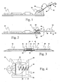
- FIGS. 1 and 2 provide examples of the problems addressed.
- lead 20 is connected to a printed circuit board 22 by a soldered connection 24.
- lead 20 is twisted (as illustrated by arrow A), repeatedly bent (as illustrated by arrows B and C), or placed into tension or compression (arrow D), a concentration of stress occurs at or near the point of connection 26.
- lead 20 may eventually weaken due to repeated deformation or cyclical movement. As a result, lead 20 will likely suffer a fatigue failure (or break) either at or near point of connection 26.
- FIG. 1 lead 20 is connected to a printed circuit board 22 by a soldered connection 24.
- arrow A As lead 20 is twisted (as illustrated by arrow A), repeatedly bent (as illustrated by arrows B and C), or placed into tension or compression (arrow D), a concentration of stress occurs at or near the point of connection 26.
- lead 20 may eventually weaken due to repeated deformation or cyclical movement.
- lead 20 will likely suffer a fatigue failure (or break) either at
- lead 20 is connected to printed circuit board 22 by a physical connector 28 that secures the connection of lead 20 by physically compressing or pinching lead 20 between crimping surfaces 30 and 32.
- lead 20 may weaken and eventually break due to repeated deformations at or near point of connection 34.
- An electrical connection more resistant to various forces and less likely to undergo fatigue failure is desirable.
- WO 99/29525 discloses an antenna for electronically transmitting pneumatic tire or wheel data, wherein the antenna comprises a continuous wire arranged in a series of loops adapted to be disposed circumferentially on a crown area of a tire.
- the wire and the transponder circuit board, to which the wire is fixes, are encased in insulating rubber. No specific precautions are met to prevent a breaking of the antenna at the connection portion with the circuit board.
- the transponder for incorporation within a tire.
- the transponder comprises a transponder circuit board and an antenna with two antenna elements.
- the antenna elements have a small spring constant in the connecting region with the transponder circuit board compared to their farther apart portions.
- US 6,546,982 B1 discloses a method and apparatus for mounting a transponder module in a tire by providing a patch with an opening extending to a cavity within the body of the patch.
- the transponder module is removably retained in the cavity by a resilient annular lip.
- US 2004/0159383 A1 describes a radio frequency device for a tire, said device comprising a radio device and an antenna.
- the radio device and the antenna may be embedded in a rubber patch, which is adhered to a surface of a tire.
- the present invention provides a method of creating a fatigue-resistant electrical connection in a tire patch with the features of claim 1 and a corresponding tire patch with the features of claim 11.
- Said electrical connection is resistant to mechanical stresses that can occur when a wire or lead is twisted or caused to bend repeatedly about its connection to a circuit.
- a material is provided that surrounds the lead and associated circuit board and in the area near the point of connection to the circuit creates a region of decreasing flexibility or graduated stiffness near the point of connection. The material is selected and configured with the lead so that it will distribute some of the mechanical stress created by movement or twisting of the lead relative to a substrate or other surface carrying the circuit to which the lead is connected.
- the lead may also be coiled or otherwise shaped to provide an additional ability to absorb and dissipate mechanical forces.
- a variety of materials may be used to create the region of graduated stiffness about the lead, and some representative examples are provided herein. Selected exemplary embodiments and methods, including preferred, of the present invention are here summarized by way of explanation of the invention and not limitation of the invention.
- a process for creating a fatigue-resistant electrical connection in which an electrical conductor having at least one end is configured for connecting to an electrical circuit.
- a predetermined area proximate such end length of the electrical conductor is configured as a stress distribution area.
- the stress distribution area is created using stress distributing materials over a predetermined length of the electrical conductor, in some cases over the entire length of the electrical conductor.
- the stress distribution area can be created in a variety of ways and may include various techniques including various forms of adhesion, gluing, and bonding of stress distributing materials and/or specialized mechanical connection methodologies.
- the end of the electrical conductor is connected to the electrical circuit. Such connection may include soldering or a mechanical connection such as a crimp.
- the electrical conductor is bonded to the stress distributing material, preferably a resilient material, along the predetermined length of the conductor. While a variety of resilient materials might be employed, some examples include rubbers or other elastomeric materials. To further enhance the stress-resistance of the circuit, the conductor may be constructed from a wire that is coiled or otherwise shaped in a manner that helps distribute stress.
- a process for assembling a strain-resistant electrical connection to an electrical circuit includes providing a resilient material capable of distributing mechanical forces completely encasing a printed circuit board and an electrical conductor connected thereto at a first end thereof to a connection point on the printed circuit board.
- the resilient material is bonded, for example, using suitable glue, to the printed circuit board and the electrical conductor.
- the first end of the electrical conductor is connected to the electrical circuit in a manner that fixes the position of the first end relative to the printed circuit board.
- the resilient material provides a transition zone for the electrical conductor in which the mobility of the conductor along the end in a direction moving along the conductor and towards the electrical circuit is gradually reduced.
- a durable connection for an electrical circuit includes a substrate supporting at least a portion of the electrical circuit.
- a conductor is included that has at least one connecting end attached to the electrical circuit.
- a resilient material is positioned proximate to the connecting end and surrounds a predetermined portion of the conductor. The resilient material is attached to the substrate and is configured for gradually restricting the mobility of the conductor along the end in a direction moving along the conductor and towards the electrical circuit.
- the present invention provides a strain-resistant electrical connection to an electrical circuit mounted on a printed circuit board that includes a transition zone for distributing stress.
- a wire conductor is provided having a first end; a portion of the conductor near the first end is coiled and embedded within a material for distributing stress.
- the wire connection point encloses at least a portion of the stress distributing material and physically contacts and restrains the wire at a location proximate to its first end so as to provide an electrical connection.
- the material for distributing stress is bonded to the printed circuit board such that the electrical conductor is substantially immovable relative to the circuit.
- the material for distributing stress is configured to provide a zone of graduated stiffness about the wire at a location proximate to the first end.
- FIG. 1 illustrates an example of an electrical connection in which a lead is soldered to a printed circuit board.
- FIG. 2 illustrates an example of an electrical connection in which a lead is mechanically connected to a printed circuit board.
- FIG. 3 illustrates a side cross section of an exemplary embodiment of the present invention.
- FIG. 4 illustrates an enlarged plan view of a portion of the exemplary embodiment illustrated in Fig. 3 .
- FIGS. 5 - 10 illustrate various exemplary stress relieving methodologies according to the present invention.
- FIGS. 3 and 4 provide side cross-section and partial plan illustrations respectively of an exemplary embodiment of the present invention.
- the particular illustrations represent a tire patch as might be used to house tire electronics for mounting in association with a tire.
- an exemplary tire electronics circuit element 36 is mounted on printed circuit board 48 and the combination is encased in an elastomeric tire patch 40.
- electrical conductors 38 are connected to circuit element 36 via solder connection 50, solder pad 51 and a plurality of terminals 37.
- Electrical conductors 38 may be coiled and may comprise a dipole antenna for the tire electronics that may, as an example only, comprise a radio frequency identification (RFID) device.
- RFID radio frequency identification
- the electrical conductors 38 are securely connected to the electronic circuit 36 by embedding at least portions 39 of the coils within solder connection 50. A portion of the electrical conductors 38 remains free from the solder, yet adjacent printed circuit board 48. This portion of the electrical conductors 38 is illustrated as residing in zone 5. Specifically, the coil portions not embedded in solder connection 50 but yet adjacent printed circuit board 48 are embedded in the elastomeric material forming patch 40. These coil portions of electrical conductor 38 within zone 5 can, within the constraints produced by the elastomeric material forming patch 40, contract, expand, or rotate so as to further reduce the concentration of stress at the point where the electrical conductor 38 enters the solder.
- electrical conductor 38 remains adjacent a rigid supporting structure to which the elastomeric material forming the patch 40 is adhered.
- the patch 40 forming elastomeric material may be adhered to electrical conductor 38 so that the combination produces a zone of graduated stiffness.
- electrical conductors 38 could also be provided with other shapes, such as, although not limited to, a sinusoidal shape, in order to improve resistance to damage caused by stress.
- tire patch itself lend important design consideration to the concept of overall stress reduction.
- tire electronics devices such as the illustrated RFID device may be installed in mechanically active areas of the tire
- designing the tire patch with the smallest possible dimensions in both thickness and surface area make the patch more compliant and reduce stresses imposed not only on the contained electronics device and connections, but also on the adhesives that may be used to secure the tire patch to the tire.
- the electrical conductors 38 may represent an antenna structure that is 1 mm thick.
- that portion of the elastomeric tire patch 40 holding the antenna may be 2 mm thick or less allowing approximately 0.5 mm of elastomeric material above and below the antenna to provide support for the antenna as well as protection from attack by chemicals and loose objects within, the tire. If any component requires more than 2 mm of height, then such components may be supported with a small "mesa" 46 in the elastomeric material with steeply sloping sides as illustrated at 42 in FIGS. 3 . In constructing a tire patch in accordance with the present invention, it is beneficial to incorporate at least a 2 mm radius of curvature wherever two or more surfaces of rubber meet, as at 42 and 44 of FIGS. 3 , to prevent a destructive buildup of stress.
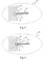
- FIGS. 5 through 10 provide illustrations of six exemplary embodiments of stress reductions methodologies for use with an electrical connection according to the present invention.
- a printed circuit board 48 as might be found in any electronics device, an electrical conductor 38 and an encasing resilient material housing 40.
- the resilient material could be a rubber or another elastomeric material having suitable properties. Using the teachings disclosed herein, one of ordinary skill in the art would understand that a variety of materials could be used for the resilient material of the housing 40.
- Housing 40 may form part or all of a tire patch or may represent adjacent portions of a tire's architecture.
- a wire or other electrical conductor 38 is connected by way of solder connection 50 to a component (not illustrated) on printed circuit board 48.
- solder connection 50 of the electrical conductor 38 to printed circuit board 48
- other connection methodologies might be employed, such as the crimped connection technique illustrated in FIG. 2 .
- a principle concept common to all the illustrated embodiments resides in the provision of a graduated stiffness in the stress distributing material surrounding the electrical connection.
- a printed circuit board 48 is used to illustrate these particular exemplary embodiments, it should be appreciated that the present invention is not limited to use with only a circuit board.
- elastomeric housing 40 is illustrated as a generally oval area surrounding the exemplary illustrated components, the housing 40, none-the-less, is designed to conform to the design principles discussed with respect to FIGS. 3 and 4 hereinabove.
- a representatively illustrated elastomeric housing 40 is shown surrounding printed circuit board 48 and electrical conductor 38.
- Electrical conductor 38 is connected to printed circuit board 48 by way of solder connection 50 within a recessed area 52 formed by sloped side walls 54.
- Elastomeric material contained within the recessed area 52 and forming a portion of the housing 40 cooperates with the walls 54 of the recessed area 52 to provide an area of increased stiffness in the vicinity of the solder connection 50.
- the electrical conductor 38 is coiled to provide, in cooperation with elastomeric material 40 and the proximity of sloped side walls 54, a graduated stress reduction zone' similar to that described with respect to FIG. 4 .
- a recess 56 is created in the printed circuit board 48 and additional stiffening wires 58 are provided and soldered into place along with electrical conductor 38.
- the additional stiffening wires 58 extent for a distance from the recess 56 into the elastomeric material forming housing 40 and thereby assist in creating a zone of increased stiffness and thereby additional stress reduction within the housing 40 at the point of connection of the electrical wire 38 to the printed circuit board 48.
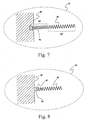
- FIG. 7 provides a variation of the FIG. 6 embodiment by providing the function of the stiffening wires 58 in the form of a section 38' of coils in the vicinity of the solder connection 50 within the coiled electrical conductor 38 having a higher pitch, i.e. having a greater number of turns per unit length, than the more remote section 38" of the electrical conductor 38.
- the higher number of turns per unit length in the area closest to the solder connection point provides a zone of increased stiffness in the area of the solder connection 50 through interaction of the elastomeric housing material by operation of the housing material surrounding a larger number of coil turns in the area of the solder connection 50 versus the number of coil turns encased in the more remote section 38" of the electrical conductor 38.
- any stress applied to electrical conductor 38 is distributed throughout its length instead of concentrating the stress in a particular location such as point of connection 50.
- the local strain on electrical conductor 38 is reduced or eliminated at or near the point of connection 50, and the likelihood of a breaking or weakening the connection at point 50 is also decreased or removed.
- the illustrated embodiment features two areas 38', 38" of varying pitch, more that two such areas may be provided and, in fact, the pitch could be continuously varied over the length of the electrical conductor 38.
- FIG. 8 yet another embodiment of the present invention is illustrated.
- additional stiffening is provided by a protrusion 60 extending from a portion of the printed circuit board 48.
- Protrusion 60 is configured such that one or more coil turns associated with the electrical conductor 38 may fit over the protrusion 60 and be connected thereto by solder connection 50.
- the presence of protrusion within a portion of the coil turns of electrical conductor 38 coupled with the surrounding elastomeric material 40 operates to produce a zone of increased stiffness and thereby functions to distribute any strain applied to the electrical conductor 38, most particularly at the solder connection 50.
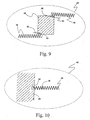
- FIG. 9 is illustrative of yet another embodiment of the present invention that is somewhat reminiscent of the embodiment illustrated in FIG. 6 . More particularly, the present embodiment makes use of a stiffening wire 62 in a manner somewhat like stiffening wires 58 illustrated in FIG. 6 . In this embodiment, however, stiffening wire 62 is actually formed by straightening a portion of the electrical conductor 38 and soldering the straightened wire and at least a portion of one of the coils of the electrical conductor 38 to the circuit board 48. The straightened portion of the electrical conductor 38 then acts in concert with the surrounding elastomeric material to provide a zone of increased stiffness in much the same manner as stiffening wire 58 of the FIG. 6 embodiment of the invention.
- FIG. 10 still yet another embodiment of the invention is illustrated which features elements much like those of several previous embodiments.
- this embodiment of the invention makes use of a straightened portion 64 of the electrical conductor 38.
- this embodiment positions that straightened portion 64 of electrical conductor 38 within several coils of the electrical conductor 38 at one end thereof.
- the straightened portion 64 operates in a manner similar to protrusion 60 of the FIG. 8 embodiment of the invention to provide, in concert with the surrounding elastomeric material, a zone of increased stiffness that provides distribution of any locally applied strain.
- electrical conductor 38 may be constructed from a material that increases the resiliency of solder connection 50.
- conductive polymer compounds, steel, stainless steel, spring steel, and spring steel coated with brass have been found by applicants to provide for a conductive and yet resilient electrical conductor 38.
- numerous other materials and shapes may be utilized as one of ordinary skill in the art will understand using the teachings disclosed herein.
- a nonconductive coating can be included around electrical conductor 38.
- a nonconductive rubber with little or no carbon black present could provide such coating.
- the elastomeric material of the housing 40 is actually bonded to the various components. That is, bonding the elastomeric material to the electrical conductor 38, for example, will increase the distribution of strain along the length of the electrical conductor 38 by insuring that the electrical conductor 38 does not slide within the elastomeric material. In addition, bonding the elastomeric material to the printed circuit board and, most especially, in the area of the solder connection 50 will assist in ensuring more uniform distribution of applied strain and thus significantly reduce the likelihood of strain induced damage to the solder connection 50 and other components within the tire electronics.
Landscapes
- Engineering & Computer Science (AREA)
- Manufacturing & Machinery (AREA)
- Mechanical Engineering (AREA)
- Microelectronics & Electronic Packaging (AREA)
- Coupling Device And Connection With Printed Circuit (AREA)
- Tires In General (AREA)
- Multi-Conductor Connections (AREA)
- Tyre Moulding (AREA)
Applications Claiming Priority (1)
| Application Number | Priority Date | Filing Date | Title |
|---|---|---|---|
| US10/932,960 US7196617B2 (en) | 2004-04-19 | 2004-09-02 | Graduated stiffness for electrical connections in tires |
Publications (3)
| Publication Number | Publication Date |
|---|---|
| EP1632369A2 EP1632369A2 (en) | 2006-03-08 |
| EP1632369A3 EP1632369A3 (en) | 2007-09-12 |
| EP1632369B1 true EP1632369B1 (en) | 2011-11-09 |
Family
ID=35467705
Family Applications (1)
| Application Number | Title | Priority Date | Filing Date |
|---|---|---|---|
| EP05107987A Expired - Lifetime EP1632369B1 (en) | 2004-09-02 | 2005-09-01 | Graduated stiffness for electrical connections in tires |
Country Status (9)
Families Citing this family (13)
| Publication number | Priority date | Publication date | Assignee | Title |
|---|---|---|---|---|
| WO2006098710A1 (en) * | 2005-03-09 | 2006-09-21 | Societe De Technologie Michelin | Robust mounting for rfid transponder antenna |
| WO2006135366A1 (en) * | 2005-06-10 | 2006-12-21 | Michelin Recherche Et Technique S.A. | Use of piezoelectric sensor attached to electronics package housing |
| FR2901422B1 (fr) * | 2006-05-19 | 2011-07-29 | Michelin Soc Tech | Module electronique destine a etre integre dans un pneumatique, dispositif comprenant un tel module, pneumatique muni d'un tel dispositif et procede d'obtention d'un tel dispositif |
| WO2009134243A1 (en) | 2008-04-29 | 2009-11-05 | Michelin Recherche Et Technique S.A. | In-plane rfid antenna |
| CN103068598B (zh) | 2010-08-30 | 2015-12-09 | 米其林集团总公司 | 弹簧定向的rfid板 |
| FR2983609B1 (fr) * | 2011-12-02 | 2014-02-07 | Michelin Soc Tech | Ensemble electronique destine a etre integre dans un pneumatique |
| WO2016056369A1 (ja) * | 2014-10-08 | 2016-04-14 | 株式会社オートネットワーク技術研究所 | コネクタ |
| CN105445328B (zh) * | 2015-12-11 | 2019-04-05 | 工业和信息化部电子第五研究所 | 综合应力下微互连焊点的疲劳寿命评价方法、装置和系统 |
| US10104937B2 (en) * | 2016-03-15 | 2018-10-23 | Nike, Inc. | Input assembly for an article of manufacture |
| RU2742062C2 (ru) * | 2016-10-04 | 2021-02-02 | Пирелли Тайр С.П.А. | Приспособление для крепления электронного устройства к шине и шина, содержащая электронное устройство |
| WO2018158897A1 (ja) * | 2017-03-01 | 2018-09-07 | オリンパス株式会社 | ケーブル実装構造体および内視鏡 |
| CN109063808A (zh) * | 2018-07-10 | 2018-12-21 | 青岛海威物联科技有限公司 | 一种rfid电子标签及加工方法 |
| JP2024139279A (ja) * | 2023-03-27 | 2024-10-09 | Toppanエッジ株式会社 | 情報読取方法 |
Citations (1)
| Publication number | Priority date | Publication date | Assignee | Title |
|---|---|---|---|---|
| US6546982B1 (en) * | 1998-08-03 | 2003-04-15 | The Goodyear Tire & Rubber Company | Mounting transponders in pneumatic tires |
Family Cites Families (33)
| Publication number | Priority date | Publication date | Assignee | Title |
|---|---|---|---|---|
| US3787806A (en) * | 1972-06-26 | 1974-01-22 | Avco Corp | Tire pressure warning apparatus |
| JPS6018996A (ja) * | 1983-07-13 | 1985-01-31 | 株式会社東芝 | 電気装置の電線口出部 |
| US4911217A (en) | 1989-03-24 | 1990-03-27 | The Goodyear Tire & Rubber Company | Integrated circuit transponder in a pneumatic tire for tire identification |
| DE4319878A1 (de) | 1992-06-17 | 1993-12-23 | Micron Technology Inc | Hochfrequenz-Identifikationseinrichtung (HFID) und Verfahren zu ihrer Herstellung |
| RU2040132C1 (ru) * | 1993-08-31 | 1995-07-20 | Владимир Вячеславович Мокрышев | Контактное устройство для соединения плоских кабелей |
| US5500065A (en) * | 1994-06-03 | 1996-03-19 | Bridgestone/Firestone, Inc. | Method for embedding a monitoring device within a tire during manufacture |
| US5971046A (en) | 1997-09-17 | 1999-10-26 | Bridgestone/Firestone, Inc. | Method and apparatus for bonding an active tag to a patch and a tire |
| DE69711100T2 (de) | 1997-12-09 | 2002-10-02 | THE GOODYEAR TIRE & RUBBER CO., AKRON | Spulenantennen für übertrager mit integriertem schaltkreis |
| US5960844A (en) | 1997-12-22 | 1999-10-05 | Bridgestone/Firestone, Inc. | Method and apparatus for monitoring conditions of a vehicle tire |
| US6217683B1 (en) | 1998-02-12 | 2001-04-17 | Michelin Recherche Et Technique S.A. | Monitored vehicle tire and monitor retainer assembly |
| US6192746B1 (en) | 1999-04-29 | 2001-02-27 | Bridgestone/Firestone Research, Inc. | Apparatus and method of providing electrical power to an active electronic device embedded within a tire |
| US6474380B1 (en) | 1999-04-29 | 2002-11-05 | Bridgestone/Firestone North American Tire, Llc | Pneumatic tire and monitoring device including dipole antenna |
| US6121880A (en) | 1999-05-27 | 2000-09-19 | Intermec Ip Corp. | Sticker transponder for use on glass surface |
| RU2161381C1 (ru) * | 1999-09-01 | 2000-12-27 | Раков Дмитрий Леонидович | Пассивный элемент электрического соединения |
| US6885291B1 (en) * | 1999-11-15 | 2005-04-26 | The Goodyear Tire & Rubber Company | Mouting transponders and antennas in pneumatic tires |
| US6462650B1 (en) | 2000-08-11 | 2002-10-08 | Raymond J. Balzer | Tire module attachment mount |
| US7190319B2 (en) * | 2001-10-29 | 2007-03-13 | Forster Ian J | Wave antenna wireless communication device and method |
| US6688353B1 (en) * | 2000-03-31 | 2004-02-10 | Bridgestone/Firestone North American Tire, Llc | Attachment patch for mounting an electronic monitoring device to the inside of a pneumatic tire |
| US6582363B2 (en) | 2000-08-25 | 2003-06-24 | Pentax Corporation | Video endoscope system and illumination optical system |
| TW560151B (en) | 2001-06-18 | 2003-11-01 | Ibm | Packet-oriented data communications between mobile and fixed data networks |
| AU2002351091A1 (en) | 2001-10-29 | 2003-05-12 | Marconi Intellectual Property (Us) Inc | Wave antenna wireless communication device |
| GB2383470B (en) * | 2001-11-12 | 2004-04-28 | Transense Technologies Plc | Self contained radio apparatus for transmission of data |
| US20040159383A1 (en) | 2002-06-11 | 2004-08-19 | Adamson John David | Method for embedding a radio frequency antenna in a tire, and an antenna for embedding in a tire |
| AU2002310385A1 (en) * | 2002-06-11 | 2003-12-22 | Michelin Recherche Et Technique S.A. | A radio frequency antenna embedded in a tire |
| US20060070570A1 (en) * | 2002-06-11 | 2006-04-06 | Man Roland Druckmaschinen Ag | Application device for a printing/painting unit in a processing machine |
| US6734791B2 (en) * | 2002-07-31 | 2004-05-11 | Michelin Recherche Et Technique S.A. | Electronics component assembly in a tire for remotely monitoring tire conditions |
| DE10300160B4 (de) * | 2003-01-07 | 2017-12-21 | Continental Reifen Deutschland Gmbh | Transponder zum Einbau in oder auf die Oberfläche eines Reifens nebst zugehörigem Reifen |
| US6847126B2 (en) | 2003-02-25 | 2005-01-25 | Michelin Recherche Et Technique S.A. | System and method for harvesting electric power from a rotating tire's static electricity |
| EP1454770A1 (en) * | 2003-03-04 | 2004-09-08 | Société de Technologie Michelin | Electronics device for a tire having an extensible antenna and a tire having such a device |
| US6772505B1 (en) | 2003-03-04 | 2004-08-10 | The Goodyear Tire & Rubber Company | Method of assembly an annular antenna to a transponder |
| US7186308B2 (en) * | 2003-10-09 | 2007-03-06 | Michelin Recherche Et Technique S.A. | System and method for providing tire electronics mounting patches |
| US20050126668A1 (en) * | 2003-12-16 | 2005-06-16 | Pierre Fornerod | Post patch for mounting devices inside tires |
| US7674117B2 (en) * | 2004-04-19 | 2010-03-09 | Michelin Recherche Et Technique S.A. | Strain-resistant electrical connection |
-
2004
- 2004-09-02 US US10/932,960 patent/US7196617B2/en not_active Expired - Fee Related
-
2005
- 2005-09-01 EP EP05107987A patent/EP1632369B1/en not_active Expired - Lifetime
- 2005-09-01 BR BRPI0504943-1A patent/BRPI0504943A/pt not_active IP Right Cessation
- 2005-09-01 JP JP2005253180A patent/JP5180431B2/ja not_active Expired - Fee Related
- 2005-09-01 AT AT05107987T patent/ATE532649T1/de active
- 2005-09-02 RU RU2005127604/09A patent/RU2369051C2/ru not_active IP Right Cessation
- 2005-09-02 KR KR1020050081619A patent/KR20060050961A/ko not_active Ceased
- 2005-09-02 CN CN2005101067584A patent/CN1767265B/zh not_active Expired - Lifetime
- 2005-09-02 TW TW094130214A patent/TW200621537A/zh unknown
Patent Citations (1)
| Publication number | Priority date | Publication date | Assignee | Title |
|---|---|---|---|---|
| US6546982B1 (en) * | 1998-08-03 | 2003-04-15 | The Goodyear Tire & Rubber Company | Mounting transponders in pneumatic tires |
Also Published As
| Publication number | Publication date |
|---|---|
| CN1767265A (zh) | 2006-05-03 |
| KR20060050961A (ko) | 2006-05-19 |
| TW200621537A (en) | 2006-07-01 |
| CN1767265B (zh) | 2010-04-07 |
| US7196617B2 (en) | 2007-03-27 |
| ATE532649T1 (de) | 2011-11-15 |
| JP5180431B2 (ja) | 2013-04-10 |
| RU2369051C2 (ru) | 2009-09-27 |
| BRPI0504943A (pt) | 2006-05-02 |
| EP1632369A3 (en) | 2007-09-12 |
| JP2006160243A (ja) | 2006-06-22 |
| RU2005127604A (ru) | 2007-03-10 |
| US20050231343A1 (en) | 2005-10-20 |
| EP1632369A2 (en) | 2006-03-08 |
Similar Documents
| Publication | Publication Date | Title |
|---|---|---|
| EP1632369B1 (en) | Graduated stiffness for electrical connections in tires | |
| US8766874B2 (en) | In-plane RFID antenna | |
| EP1589614A1 (en) | Strain-resistant electrical connection | |
| US8138924B2 (en) | Robust mounting for RFID transponder antenna | |
| JP5604593B2 (ja) | バネ型rfidボード | |
| US20120248201A1 (en) | Dual-interface smart card | |
| EP1444105B1 (en) | Self-contained radio apparatus for transmission of data | |
| JP3818174B2 (ja) | ボタン型電池用ターミナル | |
| EP3688668B1 (en) | Strap mounting techniques for wire format antennas | |
| CN111767976A (zh) | 一种植入式电子标签 | |
| US8202132B2 (en) | Contact spring for vehicular antenna/amplifier connection | |
| US9184520B2 (en) | Electrical connector | |
| KR101005767B1 (ko) | 전기적 접속을 위한 핀 | |
| JPH07272780A (ja) | フレキシブルフラットケーブル | |
| JPH08273726A (ja) | 電気コネクタおよびその製造方法 |
Legal Events
| Date | Code | Title | Description |
|---|---|---|---|
| PUAI | Public reference made under article 153(3) epc to a published international application that has entered the european phase |
Free format text: ORIGINAL CODE: 0009012 |
|
| AK | Designated contracting states |
Kind code of ref document: A2 Designated state(s): AT BE BG CH CY CZ DE DK EE ES FI FR GB GR HU IE IS IT LI LT LU LV MC NL PL PT RO SE SI SK TR |
|
| AX | Request for extension of the european patent |
Extension state: AL BA HR MK YU |
|
| PUAL | Search report despatched |
Free format text: ORIGINAL CODE: 0009013 |
|
| AK | Designated contracting states |
Kind code of ref document: A3 Designated state(s): AT BE BG CH CY CZ DE DK EE ES FI FR GB GR HU IE IS IT LI LT LU LV MC NL PL PT RO SE SI SK TR |
|
| AX | Request for extension of the european patent |
Extension state: AL BA HR MK YU |
|
| 17P | Request for examination filed |
Effective date: 20080215 |
|
| 17Q | First examination report despatched |
Effective date: 20080313 |
|
| AKX | Designation fees paid |
Designated state(s): AT BE BG CH CY CZ DE DK EE ES FI FR GB GR HU IE IS IT LI LT LU LV MC NL PL PT RO SE SI SK TR |
|
| GRAP | Despatch of communication of intention to grant a patent |
Free format text: ORIGINAL CODE: EPIDOSNIGR1 |
|
| GRAS | Grant fee paid |
Free format text: ORIGINAL CODE: EPIDOSNIGR3 |
|
| GRAA | (expected) grant |
Free format text: ORIGINAL CODE: 0009210 |
|
| AK | Designated contracting states |
Kind code of ref document: B1 Designated state(s): AT BE BG CH CY CZ DE DK EE ES FI FR GB GR HU IE IS IT LI LT LU LV MC NL PL PT RO SE SI SK TR |
|
| REG | Reference to a national code |
Ref country code: GB Ref legal event code: FG4D |
|
| REG | Reference to a national code |
Ref country code: CH Ref legal event code: EP |
|
| REG | Reference to a national code |
Ref country code: IE Ref legal event code: FG4D |
|
| REG | Reference to a national code |
Ref country code: DE Ref legal event code: R096 Ref document number: 602005031077 Country of ref document: DE Effective date: 20120119 |
|
| REG | Reference to a national code |
Ref country code: NL Ref legal event code: VDEP Effective date: 20111109 |
|
| LTIE | Lt: invalidation of european patent or patent extension |
Effective date: 20111109 |
|
| PG25 | Lapsed in a contracting state [announced via postgrant information from national office to epo] |
Ref country code: IS Free format text: LAPSE BECAUSE OF FAILURE TO SUBMIT A TRANSLATION OF THE DESCRIPTION OR TO PAY THE FEE WITHIN THE PRESCRIBED TIME-LIMIT Effective date: 20120309 Ref country code: LT Free format text: LAPSE BECAUSE OF FAILURE TO SUBMIT A TRANSLATION OF THE DESCRIPTION OR TO PAY THE FEE WITHIN THE PRESCRIBED TIME-LIMIT Effective date: 20111109 |
|
| PG25 | Lapsed in a contracting state [announced via postgrant information from national office to epo] |
Ref country code: LV Free format text: LAPSE BECAUSE OF FAILURE TO SUBMIT A TRANSLATION OF THE DESCRIPTION OR TO PAY THE FEE WITHIN THE PRESCRIBED TIME-LIMIT Effective date: 20111109 Ref country code: SI Free format text: LAPSE BECAUSE OF FAILURE TO SUBMIT A TRANSLATION OF THE DESCRIPTION OR TO PAY THE FEE WITHIN THE PRESCRIBED TIME-LIMIT Effective date: 20111109 Ref country code: BE Free format text: LAPSE BECAUSE OF FAILURE TO SUBMIT A TRANSLATION OF THE DESCRIPTION OR TO PAY THE FEE WITHIN THE PRESCRIBED TIME-LIMIT Effective date: 20111109 Ref country code: PT Free format text: LAPSE BECAUSE OF FAILURE TO SUBMIT A TRANSLATION OF THE DESCRIPTION OR TO PAY THE FEE WITHIN THE PRESCRIBED TIME-LIMIT Effective date: 20120309 Ref country code: GR Free format text: LAPSE BECAUSE OF FAILURE TO SUBMIT A TRANSLATION OF THE DESCRIPTION OR TO PAY THE FEE WITHIN THE PRESCRIBED TIME-LIMIT Effective date: 20120210 Ref country code: SE Free format text: LAPSE BECAUSE OF FAILURE TO SUBMIT A TRANSLATION OF THE DESCRIPTION OR TO PAY THE FEE WITHIN THE PRESCRIBED TIME-LIMIT Effective date: 20111109 Ref country code: NL Free format text: LAPSE BECAUSE OF FAILURE TO SUBMIT A TRANSLATION OF THE DESCRIPTION OR TO PAY THE FEE WITHIN THE PRESCRIBED TIME-LIMIT Effective date: 20111109 Ref country code: PL Free format text: LAPSE BECAUSE OF FAILURE TO SUBMIT A TRANSLATION OF THE DESCRIPTION OR TO PAY THE FEE WITHIN THE PRESCRIBED TIME-LIMIT Effective date: 20111109 |
|
| PG25 | Lapsed in a contracting state [announced via postgrant information from national office to epo] |
Ref country code: CY Free format text: LAPSE BECAUSE OF FAILURE TO SUBMIT A TRANSLATION OF THE DESCRIPTION OR TO PAY THE FEE WITHIN THE PRESCRIBED TIME-LIMIT Effective date: 20111109 |
|
| PG25 | Lapsed in a contracting state [announced via postgrant information from national office to epo] |
Ref country code: EE Free format text: LAPSE BECAUSE OF FAILURE TO SUBMIT A TRANSLATION OF THE DESCRIPTION OR TO PAY THE FEE WITHIN THE PRESCRIBED TIME-LIMIT Effective date: 20111109 Ref country code: DK Free format text: LAPSE BECAUSE OF FAILURE TO SUBMIT A TRANSLATION OF THE DESCRIPTION OR TO PAY THE FEE WITHIN THE PRESCRIBED TIME-LIMIT Effective date: 20111109 Ref country code: SK Free format text: LAPSE BECAUSE OF FAILURE TO SUBMIT A TRANSLATION OF THE DESCRIPTION OR TO PAY THE FEE WITHIN THE PRESCRIBED TIME-LIMIT Effective date: 20111109 Ref country code: BG Free format text: LAPSE BECAUSE OF FAILURE TO SUBMIT A TRANSLATION OF THE DESCRIPTION OR TO PAY THE FEE WITHIN THE PRESCRIBED TIME-LIMIT Effective date: 20120209 Ref country code: CZ Free format text: LAPSE BECAUSE OF FAILURE TO SUBMIT A TRANSLATION OF THE DESCRIPTION OR TO PAY THE FEE WITHIN THE PRESCRIBED TIME-LIMIT Effective date: 20111109 |
|
| PG25 | Lapsed in a contracting state [announced via postgrant information from national office to epo] |
Ref country code: RO Free format text: LAPSE BECAUSE OF FAILURE TO SUBMIT A TRANSLATION OF THE DESCRIPTION OR TO PAY THE FEE WITHIN THE PRESCRIBED TIME-LIMIT Effective date: 20111109 |
|
| PLBE | No opposition filed within time limit |
Free format text: ORIGINAL CODE: 0009261 |
|
| STAA | Information on the status of an ep patent application or granted ep patent |
Free format text: STATUS: NO OPPOSITION FILED WITHIN TIME LIMIT |
|
| REG | Reference to a national code |
Ref country code: AT Ref legal event code: MK05 Ref document number: 532649 Country of ref document: AT Kind code of ref document: T Effective date: 20111109 |
|
| 26N | No opposition filed |
Effective date: 20120810 |
|
| REG | Reference to a national code |
Ref country code: DE Ref legal event code: R097 Ref document number: 602005031077 Country of ref document: DE Effective date: 20120810 |
|
| PG25 | Lapsed in a contracting state [announced via postgrant information from national office to epo] |
Ref country code: AT Free format text: LAPSE BECAUSE OF FAILURE TO SUBMIT A TRANSLATION OF THE DESCRIPTION OR TO PAY THE FEE WITHIN THE PRESCRIBED TIME-LIMIT Effective date: 20111109 |
|
| PG25 | Lapsed in a contracting state [announced via postgrant information from national office to epo] |
Ref country code: MC Free format text: LAPSE BECAUSE OF NON-PAYMENT OF DUE FEES Effective date: 20120930 Ref country code: ES Free format text: LAPSE BECAUSE OF FAILURE TO SUBMIT A TRANSLATION OF THE DESCRIPTION OR TO PAY THE FEE WITHIN THE PRESCRIBED TIME-LIMIT Effective date: 20120220 |
|
| REG | Reference to a national code |
Ref country code: CH Ref legal event code: PL |
|
| GBPC | Gb: european patent ceased through non-payment of renewal fee |
Effective date: 20120901 |
|
| REG | Reference to a national code |
Ref country code: IE Ref legal event code: MM4A |
|
| PG25 | Lapsed in a contracting state [announced via postgrant information from national office to epo] |
Ref country code: FI Free format text: LAPSE BECAUSE OF FAILURE TO SUBMIT A TRANSLATION OF THE DESCRIPTION OR TO PAY THE FEE WITHIN THE PRESCRIBED TIME-LIMIT Effective date: 20111109 |
|
| PG25 | Lapsed in a contracting state [announced via postgrant information from national office to epo] |
Ref country code: GB Free format text: LAPSE BECAUSE OF NON-PAYMENT OF DUE FEES Effective date: 20120901 Ref country code: LI Free format text: LAPSE BECAUSE OF NON-PAYMENT OF DUE FEES Effective date: 20120930 Ref country code: CH Free format text: LAPSE BECAUSE OF NON-PAYMENT OF DUE FEES Effective date: 20120930 Ref country code: IE Free format text: LAPSE BECAUSE OF NON-PAYMENT OF DUE FEES Effective date: 20120901 |
|
| PG25 | Lapsed in a contracting state [announced via postgrant information from national office to epo] |
Ref country code: TR Free format text: LAPSE BECAUSE OF FAILURE TO SUBMIT A TRANSLATION OF THE DESCRIPTION OR TO PAY THE FEE WITHIN THE PRESCRIBED TIME-LIMIT Effective date: 20111109 |
|
| PG25 | Lapsed in a contracting state [announced via postgrant information from national office to epo] |
Ref country code: LU Free format text: LAPSE BECAUSE OF NON-PAYMENT OF DUE FEES Effective date: 20120901 |
|
| PG25 | Lapsed in a contracting state [announced via postgrant information from national office to epo] |
Ref country code: HU Free format text: LAPSE BECAUSE OF FAILURE TO SUBMIT A TRANSLATION OF THE DESCRIPTION OR TO PAY THE FEE WITHIN THE PRESCRIBED TIME-LIMIT Effective date: 20050901 |
|
| REG | Reference to a national code |
Ref country code: FR Ref legal event code: PLFP Year of fee payment: 12 |
|
| REG | Reference to a national code |
Ref country code: FR Ref legal event code: PLFP Year of fee payment: 13 |
|
| REG | Reference to a national code |
Ref country code: FR Ref legal event code: PLFP Year of fee payment: 14 |
|
| REG | Reference to a national code |
Ref country code: DE Ref legal event code: R081 Ref document number: 602005031077 Country of ref document: DE Owner name: COMPAGNIE GENERALE DES ETABLISSEMENTS MICHELIN, FR Free format text: FORMER OWNERS: SOCIETE DE TECHNOLOGIE MICHELIN, CLERMONT-FERRAND, FR; MICHELIN RECHERCHE ET TECHNIQUE S.A., GRANGES-PACCOT, CH |
|
| PGFP | Annual fee paid to national office [announced via postgrant information from national office to epo] |
Ref country code: DE Payment date: 20240918 Year of fee payment: 20 |
|
| PGFP | Annual fee paid to national office [announced via postgrant information from national office to epo] |
Ref country code: FR Payment date: 20240924 Year of fee payment: 20 |
|
| PGFP | Annual fee paid to national office [announced via postgrant information from national office to epo] |
Ref country code: IT Payment date: 20240924 Year of fee payment: 20 |
|
| REG | Reference to a national code |
Ref country code: DE Ref legal event code: R071 Ref document number: 602005031077 Country of ref document: DE |