EP1622367B1 - Solid-state imaging device - Google Patents
Solid-state imaging device Download PDFInfo
- Publication number
- EP1622367B1 EP1622367B1 EP04727421A EP04727421A EP1622367B1 EP 1622367 B1 EP1622367 B1 EP 1622367B1 EP 04727421 A EP04727421 A EP 04727421A EP 04727421 A EP04727421 A EP 04727421A EP 1622367 B1 EP1622367 B1 EP 1622367B1
- Authority
- EP
- European Patent Office
- Prior art keywords
- solid
- state imaging
- ccd chip
- package
- imaging apparatus
- Prior art date
- Legal status (The legal status is an assumption and is not a legal conclusion. Google has not performed a legal analysis and makes no representation as to the accuracy of the status listed.)
- Expired - Lifetime
Links
- 238000003384 imaging method Methods 0.000 title claims abstract description 70
- 230000005669 field effect Effects 0.000 claims description 12
- 125000006850 spacer group Chemical group 0.000 abstract description 7
- 239000000203 mixture Substances 0.000 description 21
- 230000008054 signal transmission Effects 0.000 description 15
- 239000000758 substrate Substances 0.000 description 13
- 230000003071 parasitic effect Effects 0.000 description 10
- 238000003491 array Methods 0.000 description 8
- 230000000694 effects Effects 0.000 description 7
- XUIMIQQOPSSXEZ-UHFFFAOYSA-N Silicon Chemical compound [Si] XUIMIQQOPSSXEZ-UHFFFAOYSA-N 0.000 description 6
- 238000013016 damping Methods 0.000 description 6
- 229910052710 silicon Inorganic materials 0.000 description 6
- 239000010703 silicon Substances 0.000 description 6
- 238000010586 diagram Methods 0.000 description 5
- 230000004048 modification Effects 0.000 description 5
- 238000012986 modification Methods 0.000 description 5
- 230000002411 adverse Effects 0.000 description 4
- 239000010408 film Substances 0.000 description 4
- 230000002093 peripheral effect Effects 0.000 description 4
- 239000000853 adhesive Substances 0.000 description 3
- 239000012790 adhesive layer Substances 0.000 description 3
- 239000000463 material Substances 0.000 description 3
- 229910052581 Si3N4 Inorganic materials 0.000 description 2
- PNEYBMLMFCGWSK-UHFFFAOYSA-N aluminium oxide Inorganic materials [O-2].[O-2].[O-2].[Al+3].[Al+3] PNEYBMLMFCGWSK-UHFFFAOYSA-N 0.000 description 2
- 239000000919 ceramic Substances 0.000 description 2
- 238000009792 diffusion process Methods 0.000 description 2
- 238000005530 etching Methods 0.000 description 2
- 238000000034 method Methods 0.000 description 2
- 230000000452 restraining effect Effects 0.000 description 2
- HQVNEWCFYHHQES-UHFFFAOYSA-N silicon nitride Chemical compound N12[Si]34N5[Si]62N3[Si]51N64 HQVNEWCFYHHQES-UHFFFAOYSA-N 0.000 description 2
- 239000007787 solid Substances 0.000 description 2
- VYPSYNLAJGMNEJ-UHFFFAOYSA-N Silicium dioxide Chemical compound O=[Si]=O VYPSYNLAJGMNEJ-UHFFFAOYSA-N 0.000 description 1
- 229910021417 amorphous silicon Inorganic materials 0.000 description 1
- 230000005540 biological transmission Effects 0.000 description 1
- 238000005219 brazing Methods 0.000 description 1
- 229910010293 ceramic material Inorganic materials 0.000 description 1
- 238000000151 deposition Methods 0.000 description 1
- 238000007599 discharging Methods 0.000 description 1
- 238000009429 electrical wiring Methods 0.000 description 1
- 238000010894 electron beam technology Methods 0.000 description 1
- 239000003822 epoxy resin Substances 0.000 description 1
- 230000001747 exhibiting effect Effects 0.000 description 1
- 229910000830 fernico Inorganic materials 0.000 description 1
- PCHJSUWPFVWCPO-UHFFFAOYSA-N gold Chemical compound [Au] PCHJSUWPFVWCPO-UHFFFAOYSA-N 0.000 description 1
- 239000010931 gold Substances 0.000 description 1
- 229910052737 gold Inorganic materials 0.000 description 1
- 229910000833 kovar Inorganic materials 0.000 description 1
- 239000002184 metal Substances 0.000 description 1
- 229910052751 metal Inorganic materials 0.000 description 1
- 238000000059 patterning Methods 0.000 description 1
- 238000000206 photolithography Methods 0.000 description 1
- 238000007747 plating Methods 0.000 description 1
- 229920000647 polyepoxide Polymers 0.000 description 1
- 229920005989 resin Polymers 0.000 description 1
- 239000011347 resin Substances 0.000 description 1
- 239000010409 thin film Substances 0.000 description 1
Images


Classifications
-
- H—ELECTRICITY
- H01—ELECTRIC ELEMENTS
- H01L—SEMICONDUCTOR DEVICES NOT COVERED BY CLASS H10
- H01L27/00—Devices consisting of a plurality of semiconductor or other solid-state components formed in or on a common substrate
- H01L27/14—Devices consisting of a plurality of semiconductor or other solid-state components formed in or on a common substrate including semiconductor components sensitive to infrared radiation, light, electromagnetic radiation of shorter wavelength or corpuscular radiation and specially adapted either for the conversion of the energy of such radiation into electrical energy or for the control of electrical energy by such radiation
- H01L27/144—Devices controlled by radiation
- H01L27/146—Imager structures
- H01L27/14601—Structural or functional details thereof
- H01L27/14618—Containers
-
- H—ELECTRICITY
- H04—ELECTRIC COMMUNICATION TECHNIQUE
- H04N—PICTORIAL COMMUNICATION, e.g. TELEVISION
- H04N25/00—Circuitry of solid-state image sensors [SSIS]; Control thereof
- H04N25/70—SSIS architectures; Circuits associated therewith
- H04N25/71—Charge-coupled device [CCD] sensors; Charge-transfer registers specially adapted for CCD sensors
- H04N25/75—Circuitry for providing, modifying or processing image signals from the pixel array
-
- H—ELECTRICITY
- H01—ELECTRIC ELEMENTS
- H01L—SEMICONDUCTOR DEVICES NOT COVERED BY CLASS H10
- H01L27/00—Devices consisting of a plurality of semiconductor or other solid-state components formed in or on a common substrate
- H01L27/14—Devices consisting of a plurality of semiconductor or other solid-state components formed in or on a common substrate including semiconductor components sensitive to infrared radiation, light, electromagnetic radiation of shorter wavelength or corpuscular radiation and specially adapted either for the conversion of the energy of such radiation into electrical energy or for the control of electrical energy by such radiation
-
- H—ELECTRICITY
- H04—ELECTRIC COMMUNICATION TECHNIQUE
- H04N—PICTORIAL COMMUNICATION, e.g. TELEVISION
- H04N25/00—Circuitry of solid-state image sensors [SSIS]; Control thereof
-
- H—ELECTRICITY
- H01—ELECTRIC ELEMENTS
- H01L—SEMICONDUCTOR DEVICES NOT COVERED BY CLASS H10
- H01L2224/00—Indexing scheme for arrangements for connecting or disconnecting semiconductor or solid-state bodies and methods related thereto as covered by H01L24/00
- H01L2224/01—Means for bonding being attached to, or being formed on, the surface to be connected, e.g. chip-to-package, die-attach, "first-level" interconnects; Manufacturing methods related thereto
- H01L2224/42—Wire connectors; Manufacturing methods related thereto
- H01L2224/47—Structure, shape, material or disposition of the wire connectors after the connecting process
- H01L2224/48—Structure, shape, material or disposition of the wire connectors after the connecting process of an individual wire connector
- H01L2224/4805—Shape
- H01L2224/4809—Loop shape
- H01L2224/48091—Arched
-
- H—ELECTRICITY
- H01—ELECTRIC ELEMENTS
- H01L—SEMICONDUCTOR DEVICES NOT COVERED BY CLASS H10
- H01L2924/00—Indexing scheme for arrangements or methods for connecting or disconnecting semiconductor or solid-state bodies as covered by H01L24/00
- H01L2924/10—Details of semiconductor or other solid state devices to be connected
- H01L2924/11—Device type
- H01L2924/13—Discrete devices, e.g. 3 terminal devices
- H01L2924/1304—Transistor
- H01L2924/1305—Bipolar Junction Transistor [BJT]
-
- H—ELECTRICITY
- H01—ELECTRIC ELEMENTS
- H01L—SEMICONDUCTOR DEVICES NOT COVERED BY CLASS H10
- H01L2924/00—Indexing scheme for arrangements or methods for connecting or disconnecting semiconductor or solid-state bodies as covered by H01L24/00
- H01L2924/15—Details of package parts other than the semiconductor or other solid state devices to be connected
- H01L2924/151—Die mounting substrate
- H01L2924/156—Material
- H01L2924/15786—Material with a principal constituent of the material being a non metallic, non metalloid inorganic material
- H01L2924/15787—Ceramics, e.g. crystalline carbides, nitrides or oxides
-
- H—ELECTRICITY
- H01—ELECTRIC ELEMENTS
- H01L—SEMICONDUCTOR DEVICES NOT COVERED BY CLASS H10
- H01L2924/00—Indexing scheme for arrangements or methods for connecting or disconnecting semiconductor or solid-state bodies as covered by H01L24/00
- H01L2924/19—Details of hybrid assemblies other than the semiconductor or other solid state devices to be connected
- H01L2924/191—Disposition
- H01L2924/19101—Disposition of discrete passive components
- H01L2924/19105—Disposition of discrete passive components in a side-by-side arrangement on a common die mounting substrate
Landscapes
- Engineering & Computer Science (AREA)
- Physics & Mathematics (AREA)
- Power Engineering (AREA)
- Multimedia (AREA)
- Signal Processing (AREA)
- Electromagnetism (AREA)
- Condensed Matter Physics & Semiconductors (AREA)
- General Physics & Mathematics (AREA)
- Computer Hardware Design (AREA)
- Microelectronics & Electronic Packaging (AREA)
- Solid State Image Pick-Up Elements (AREA)
- Transforming Light Signals Into Electric Signals (AREA)
Abstract
Description
- The present invention relates to a solid-state imaging apparatus.
- There is known a solid-state imaging apparatus comprising: a solid-state imaging element, having an energy ray sensitive portion; and a package, housing the solid-state imaging element; and having signal processing circuits, which process signals output from the above-mentioned solid-state imaging element and are disposed at the exterior of the package (see, for example, Patent Document 1)
European patent numberEP0828398 describes an imaging apparatus where a solid state imaging device chip is bonded to the surface of a substrate alongside a peripheral circuit which is also bonded to the substrate. The solid state imaging device chip is connected to the peripheral circuit via thin metal wires.
Japanese patent numberJP 2002 368949 - [Patent Document 1] Japanese Published Unexamined Patent Application No.
H4-317280 - However, when the signal processing circuits are disposed at the exterior of the package, the signal transmission paths (electrical wirings) from the solid-state imaging element to the signal processing circuits become long and the parasitic capacitance of the signal transmission paths becomes large. As a result, the waveforms of the signals output from the solid-state imaging element become damped and high-speed response properties are degraded.
- The present invention has been accomplished in view of the above point and an object of the invention is to provide a solid-state imaging apparatus, with which the parasitic capacitance of signal transmission paths is reduced to enable restraining of the damping of the waveforms of signals output from a solid-state imaging element and improvement of the high-speed response properties.
- In order to achieve the above object, a solid-state imaging apparatus according to the present invention is defined in
claim 1. - In the solid-state imaging apparatus according to the present invention, the signal processing circuit is positioned proximally to the solid-state imaging element by making use of the step difference between the first planar portion and the second planar portion. Signal transmission path from the solid-state imaging element to the signal processing circuit is thereby made short and the parasitic capacitance of the signal transmission path is made small. As a result, the damping of the waveforms of the signal output from the solid-state imaging element can be restrained and the high-speed response properties can be improved.
- As described above, the solid-state imaging apparatus is provided with which the parasitic capacitance of the signal transmission path is reduced to enable restraining of the damping of the waveforms of the signal output from the solid-state imaging element and improvement of the high-speed response properties.
- With the composition of the solid-state imaging apparatus of the present invention, since the solid-state imaging element and the load resistor are positioned apart from each other, even if the load resistor generate heat, adverse effects on the characteristics of the solid-state imaging element (for example, increasing of the dark current) can be prevented.
- Preferably, one end of the load resistor is electrically connected to an output terminal of the solid-state imaging element and the other end is grounded, and a buffer amplifier , having a bipolar transistor that is electrically connected to the output terminal of the solid-state imaging element. With the composition, since the solid-state imaging element and the load resistor are positioned apart from each other, even if the load resistor generates heat, adverse effects on the characteristics of the solid-state imaging element (for example, increasing of the dark current) can be prevented. Also, since the bipolar transistor is high in driving ability with respect to the load resistor, effects due to the parasitic capacitance of the signal transmission path subsequent the buffer amplifier can be alleviated.
-
FIG. 1 is a schematic view for describing the sectional composition of a solid-state imaging apparatus of a first embodiment. -
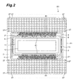
FIG. 2 is a plan view of the solid-state imaging apparatus of the first embodiment. -
FIG. 3 is a circuit diagram for describing the composition of a signal processing circuit. -
FIG. 4A is a schematic view showing a solid-state imaging apparatus of a conventional art. -
FIG. 4B is a schematic view showing the solid-state imaging apparatus of the first embodiment. -
FIG. 5 is a schematic view for describing the sectional composition of a solid-state imaging apparatus of a second embodiment. -
FIG. 6 is a plan view of the solid-state imaging apparatus of the second embodiment. -
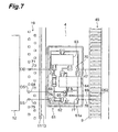
FIG. 7 is a plan view showing the composition of the vicinity of the buffer amplifier module shown inFIG. 6 . -
FIG. 8 is a circuit diagram for describing the composition of the buffer amplifier module. -
FIG. 9A is a schematic view showing a solid-state imaging apparatus of a conventional art. -
FIG. 9B is a schematic view showing the solid-state imaging apparatus of the second embodiment. -
FIG. 10 is a schematic view for describing the sectional composition of a modification example of the solid-state imaging apparatus of the second embodiment. - Solid-state imaging apparatuses of embodiments of the present invention shall now be described with reference to the drawings. Identical elements or elements with identical functionality will be denoted by the same reference symbols in the description, without redundant description.
- First, the composition of a solid-state imaging apparatus of a first embodiment shall be described based on
FIGS. 1 to 3 .FIG. 1 is a schematic view for describing the sectional composition of the solid-state imaging apparatus of the first embodiment.FIG. 2 is a plan view of the same solid-state imaging apparatus of the first embodiment.FIG. 3 is a circuit diagram for describing the composition of a signal processing circuit.FIG. 2 is a view viewed from a back surface (side opposite the side onto which energy rays are made incident) of the solid-state imaging apparatus. - A solid-state imaging apparatus IS1 of the first embodiment comprises a ceramic package P1, a back-illuminated CCD chip 11 (solid-state imaging element),
chip resistor arrays 21, etc. At a central portion of package P1 is formed ahollow portion 1, which extends in a predetermined direction of package P1. In package P1, amounting portion 2, for mountingCCD chip 11 andchip resistor arrays 21, is disposed so as to protrude intohollow portion 1.Mounting portion 2 has a firstplanar portion 3 for positioning ofCCD chip 11 and secondplanar portions 4 for positioning ofchip resistor arrays 21. Firstplanar portion 3 and secondplanar portions 4 are formed to be stepped with respect to each other. -
Mounting portion 2 furthermore has a thirdplanar portion 5 and a fourthplanar portion 6. Thirdplanar portion 5 is positioned between firstplanar portion 3 and secondplanar portions 4 and is formed to be stepped with respect to firstplanar portion 3 and secondplanar portions 4. Fourthplanar portion 6 is positioned between aback surface 7 of package P1 and secondplanar portions 4 and is formed to be stepped with respect toback surface 7 of package P1 and secondplanar portions 4. A plurality ofelectrode pins 27 for external connection are positioned onback surface 7 of package P1. -
CCD chip 11 has an energy raysensitive portion 12, which converts incident energy rays into charges.CCD chip 11 is mounted on firstplanar portion 3 ofmounting portion 2 via aspacer 13 so that the back surface will be the energy ray incident surface and is fixed onto the mounting portion 2 (package P1). CCD chip 11is formed of a silicon substrate of a thickness of approximately 300µm. With back-illuminated CCD chip 11, the substrate must be made thin and a potential slope must be formed from the incident surface (back surface) side. - At a back surface side region (inner side region) of
CCD chip 11 that includes a region corresponding to energy raysensitive portion 12, athin portion 14, which is thinned to a thickness of approximately 10 to 30µm (that is, etched to a depth of approximately 270 to 290µm), is formed. A structure having such athin portion 14 is formed by depositing a silicon nitride film onto the silicon substrate, patterning the film to a desired shape by a photolithography process, and using the film as a mask to etch the silicon substrate using an etching solution, comprising KOH, while leaving the peripheral portion of the substrate, which is covered by the silicon nitride film, in the thick state. -
Spacer 13 is formed of a material that has a higher thermal expansion coefficient at a predetermined temperature range (for example, 133°C) than the thermal expansion coefficient of CCD chip 11 (silicon), and in the present embodiment, is formed of alumina or other ceramic material. The thermal expansion coefficient of silicon at 133°C is 2.5 × 10⁻⁶(/°C) and the thermal expansion coefficient of alumina at 133°C is 6.5 × 10⁻⁶(/°C).Spacer 13 is adhered and fixed to package P1 by an adhesive agent (not shown). Also, the back surface side of aframe portion 15 ofCCD chip 11 is adhered and fixed to spacer 13 by an adhesive agent (not shown). - On front surface (energy ray incident side surface) 8 of package P1 at the periphery of
hollow portion 1, aseal ring 31 is fixed by brazing, etc., so as to surround hollow portion 1 (CCD chip 11). Acap 32 is seam-welded toseal ring 31. As mentioned above,cap 32 has its outer peripheral portion mounted on and seam-welded toseal ring 31 and has an openingportion 33, provided at a position opposingthin portion 14 ofCCD chip 11.Cap 32 is formed integrally of kovar (fernico) and a gold plating is applied to itsfront surface 8. - A
window member 34, which allows the transmission of energy rays (light, electron beam, etc.), is fixed to cap 32 so as to cover openingportion 33.Window member 34 is formed of a plate-like quartz glass base material, is arranged to transmit ultraviolet rays, and its energy ray incident surface and energy ray exit surface are polished. Also,window member 34 is fixed to cap 32 by the end portions of the energy ray incident surface being fixed across the entire periphery onto the upper surface (the surface at the side opposite the surface opposing CCD chip 11) ofcap 32 via an adhesive layer (not shown). - Though not illustrated, the portion of
hollow portion 1 of package P1 at the opposite side of the energy ray incident side portion may be sealed by a bottom cover or by filling with a resin material, etc. - A plurality of first
package side electrodes 41, for connection with CCD chip side electrodes (not shown) ofCCD chip 11, are disposed on third flat portion of mountingportion 2. Each firstpackage side electrode 41 is electrically connected to a predetermined electrode pin among a plurality of electrode pins 27 via an internal wiring (not shown) formed inside package P1. The CCD chip side electrodes and firstpackage side electrodes 41 are electrically connected via bonding wires (not shown). Transfer signals and other signals are thus sent from the exterior toCCD chip 11 via predetermined electrode pins, internal wirings, firstpackage side electrodes 41, bonding wires, and CCD chip side electrodes. - Each
chip resistor array 21 has a plurality ofresistors 22, which are formed in array form on asubstrate 21a. Onsubstrate 21a, an input terminal (input electrode) 23 and an output terminal (output electrode) 24 are formed for eachresistor 22. Eachchip resistor array 21 is mounted on a secondplanar portion 4 of mountingportion 2 via an adhesive layer (not shown) and is thereby fixed to mounting portion 2 (package P1).Input terminals 23 are electrically connected viabonding wires 42 to output terminals (electrodes) OS ofCCD chip 11. - On fourth
flat portion 6 of mountingportion 2 is disposed a plurality of secondpackage side electrodes 43 for connection tooutput terminals 24 ofchip resistor array 21. Each secondpackage side electrode 43 is electrically connected to a predetermined electrode pin among the plurality of electrode pins 27 via an internal wiring formed inside package P1.Output terminals 24 and secondpackage side electrodes 43 are electrically connected viabonding wires 44. Signals are thus sent fromCCD chip 11 to the exterior via output terminals OS ofCCD chip 11,bonding wires 42, chip resistor arrays 21 (resistors 22),bonding wires 44, secondpackage side electrodes 43, internal wirings, and predetermined electrode pins. - The signal processing circuits for processing signals output from
CCD chip 11 shall now be described with reference toFIG. 3 . - Each signal processing circuit has
resistor 22, which is included inchip resistor array 21, and anoperational amplifier 51.Operational amplifier 51 is formed on an external substrate (not shown), etc., onto which solid-state imaging apparatus IS 1 (package P1) is mounted. -
CCD chip 11 has field-effect transistors 16 for reading potential variations of floating diffusions (not shown), and the gate terminal of each field-effect transistor 16 is electrically connected to the floating diffusion. The source terminal of each field-effect transistor 16 is electrically connected to output terminal OS ofCCD chip 11 and is connected via the output terminal OS to inputterminal 23 ofresistor 22. The drain terminal of each field-effect transistor 16 is electrically connected to a terminal OD, and a voltage that exhibits a fixed positive voltage value is input into the terminal OD. Here,resistor 22 acts as a load resistor and field-effect transistor 16 andresistor 22 make up a source follower circuit. -
Output terminal 24 ofresistor 22 is electrically connected to the inverted input terminal ofoperational amplifier 51. Aresistor 52 is disposed between the inverted input terminal and the output terminal ofoperational amplifier 51, and a variable voltage supply 53 is electrically connected to the non-inverted input terminal ofoperational amplifier 51. The inverted input terminal and the non-inverted input terminal ofoperational amplifier 51 are in a virtually shorted relationship. - With the present embodiment, a shielding
member 35 is positioned with respect toCCD chip 11 so as to shield the front side in the energy ray incident direction of a beveled portion (the inclined portion betweenthin portion 14 and frame portion 15) ofCCD chip 11. The shieldingmember 35 is formed of a silicon substrate of approximately 300µm thickness and blocks energy rays (such as light). A throughhole 36 of rectangular shape is formed by etching, etc., at a position of shieldingmember 35 that opposesthin portion 14. Shieldingmember 35 is adhered and fixed to theback surface 7 side offrame portion 15 ofCCD chip 11 by an adhesive agent (not shown), formed of epoxy resin, etc. A recessed portion, which holds shieldingmember 35 in the state in whichCCD chip 11 andspacer 13 are adhered and fixed, is formed at a position ofspacer 13 that corresponds to shieldingmember 35, fixed to frameportion 15 ofCCD chip 11, so as to surround the entire periphery of shieldingmember 35. - As described above, with the present embodiment,
chip resistor arrays 21 are positioned on secondplanar portions 4, which differ from firstplanar portion 3 on whichCCD chip 11 is positioned, and using the step difference between firstplanar portion 3 and secondplanar portions 4,CCD chip 11 andchip resistor arrays 21 are positioned proximally. Thus in comparison to a composition (seeFIG. 4A ), wherein a plurality of resistors (load resistors) 103 are positioned outside a solid-state imaging apparatus 101, the signal transmission paths fromCCD chip 11 to chip resistor arrays 21 (resistors 22) are made shorter and the parasitic capacitance of the signal transmission paths is made smaller in solid-state imaging apparatus IS1 of the present embodiment (seeFIG. 4B ). As a result, the damping of the waveforms of the signals output fromCCD chip 11 can be restrained and the high speed response properties can be improved. - Also with the present embodiment, each
chip resistor array 21 includesresistors 22 that are electrically connected to output terminals OS ofCCD chip 11. With the composition, sinceresistors 22 that function as load resistors are positioned away fromCCD chip 11, even whenresistors 22 generate heat, adverse effects on the characteristics of CCD chip 11 (for example, increasing of the dark current) can be prevented. - Since the inverted input terminal and the non-inverted input terminal of each
operational amplifier 51 is in a virtually shorted relationship, the electric potential here is always fixed. Charging and discharging of charges therefore will not occur and effects due to the parasitic capacitance of the signal transmission paths fromchip resistor arrays 21 tooperational amplifier 51 can be neglected substantially. - The composition of a solid-state imaging apparatus of a second embodiment shall now be described based on
FIGS. 5 to 8 .FIG. 5 is a schematic view for describing the sectional composition of the solid-state imaging apparatus of the second embodiment.FIG. 6 is a plan view of the same solid-state imaging apparatus of the second embodiment.FIG. 7 is a plan view showing the composition of the vicinity of a buffer amplifier module.FIG. 8 is a circuit diagram for describing the composition of the buffer amplifier module.FIGS. 6 and7 are diagrams of the solid-state imaging apparatus as viewed from the back surface side. - A solid-state imaging apparatus IS2 of the second embodiment comprises a package P2,
CCD chip 11,buffer amplifier modules 61, which serve as signal processing circuits, etc. - Mounting
portion 2 has a firstplanar portion 3 forpositioning CCD chip 11, secondplanar portions 4 for positioningbuffer amplifier modules 61, and a thirdplanar portion 9. Thirdplanar portion 9 is positioned betweenback surface 7 of package P2 and secondplanar portions 4 and is formed to be stepped with respect to backsurface 7 of package P2 and secondplanar portions 4. The portion ofhollow portion 1 of package P2 at the opposite side of the energy ray incident side portion is sealed by abottom cover 10. - A plurality of
package side electrodes 45 are disposed on thirdplanar portion 9 of mountingportion 2. Eachpackage side electrode 45 is electrically connected to a predetermined electrode pin among the plurality of electrode pins 27 via an internal wiring (not shown) formed inside package P2. Predetermined electrodes among CCDchip side electrodes 19, formed onCCD chip 11, are electrically connected viabonding wires 46 to predetermined electrodes amongpackage side electrodes 45. Transfer signals and other signals are thus sent from the exterior toCCD chip 11 via predetermined electrode pins, internal wirings, predetermined package side electrodes,bonding wires 46, and predetermined CCD chip side electrodes. - As shown in
FIGS. 7 and8 , eachbuffer amplifier module 61 comprises aload resistor 62, abipolar transistor 63, and a field-effect transistor 64, andload resistor 62,bipolar transistor 63, and field-effect transistor 64 are positioned on asubstrate 61a. Each buffer amplifier module 61 (substrate 61 a) is mounted via an adhesive layer (not shown) on a secondplanar portion 4 of mountingportion 2 and is thereby fixed to the mounting portion 2 (package P2). - An output terminal OS1 (source terminal of a field-effect transistor 16) of
CCD chip 11 is electrically connected to an input terminal (electrode) 65 of abuffer amplifier module 61. One terminal ofload resistor 62 is electrically connected viainput terminal 65 to output terminal OS1 ofCCD chip 11 and the other terminal ofload resistor 62 is grounded. - The base terminal of
bipolar transistor 63 is electrically connected viainput terminal 65 and aresistor 66 to output terminal OS1 ofCCD chip 11, and the emitter terminal is electrically connected to the drain terminal of field-effect transistor 64 and an output terminal (electrode) 67 ofbuffer amplifier module 61. The collector terminal ofbipolar transistor 63 is electrically connected to a terminal (electrode) 70. As with terminal OD, a voltage, exhibiting a fixed positive voltage value, is input intoterminal 70. The gate terminal and source terminal offield effect transistor 64 are grounded.Resistor element 66 is for controlling the base current ofbipolar transistor 63. Here,field effect transistor 16 andload resistor 62 make up a source follower circuit. - Output terminal OS1 of
CCD chip 11 andinput terminal 65 ofbuffer amplifier module 61 are connected via abonding wire 68.Output terminal 67 ofbuffer amplifier module 61 is connected via abonding wire 69 to a predetermined package side electrode OS2. Terminal OD is connected via a bonding wire 71 to aterminal 72 ofbuffer amplifier module 61 and is electrically connected toterminal 70.Terminal 70 is connected via a bonding wire 74 to a predetermined package side electrode. - A terminal SS of the CCD chip is connected via a bonding wire 75 to a terminal (electrode) 76 of
buffer amplifier module 61, and a terminal (electrode) 77 that is electrically connected to the terminal 76 is connected via abonding wire 78 to a predetermined package side electrode. The predetermined package side electrode is electrically connected to a predetermined electrode pin (ground pin) among electrode pins 27 that is grounded. - As described above, with the present embodiment,
buffer amplifier modules 61 are positioned on secondplanar portions 4, which differ from firstplanar portion 3 on whichCCD chip 11 is positioned, and using the step difference between firstplanar portion 3 and secondplanar portions 4,CCD chip 11 andbuffer amplifier modules 61 are positioned proximally. Thus in comparison to a composition whereinbuffer amplifier modules 203 are positioned outside a solid-state imaging apparatus 201 (seeFIG. 9A ), the present embodiment's solid-state imaging apparatus IS2 (seeFIG. 9B ) is made shorter in the signal transmission paths fromCCD chip 11 to bufferamplifier modules 61 and thus made smaller in the parasitic capacitance of the signal transmission paths. As a result, the damping of the waveforms of signals output fromCCD chip 11 can be restrained and the high-speed response properties can be improved.Buffer amplifier modules 203 inFIG. 9A have the same composition asbuffer amplifier modules 61 of the present embodiment. - Also, each
buffer amplifier module 61 includesload resistor 62, which has one end connected to output terminal OS1 of CCD chip 11I and the other end grounded, andbipolar transistor 63, which is electrically connected tooutput terminal OS 1 ofCCD chip 11. With the composition, sinceCCD chip 11 andload resistor 62 are positioned apart from each other, even whenload resistor 62 generates heat, adverse effects on the characteristics of CCD chip 11 (such as the increasing of the dark current) can be prevented. Also, sincebipolar transistor 63 is high in driving ability with respect to loadresistor 62, effects due to the parasitic capacitance of the signal transmission path subsequentbuffer amplifier module 61 can be alleviated. - A modification example of the solid-state imaging apparatus of the second embodiment shall now be described with reference to
FIG. 10. FIG. 10 is a schematic view for describing the sectional composition of the modification example of the solid-state imaging apparatus of the second embodiment. - A solid-state imaging apparatus IS3 of the modification example of the second embodiment comprises a package P3, a front-illuminated
CCD chip 81,buffer amplifier modules 61, which serve as signal processing circuits, etc. - Package P3 has a recessed
portion 93, which is surrounded by abottom portion 91 and aside portion 92, and is made of ceramic as with the above-described packages P1 and P2.Bottom portion 91 has a firstplanar portion 94 forpositioning CCD chip 81 and secondplanar portions 95 for positioningbuffer amplifier modules 61. Firstplanar portion 94 and secondplanar portions 95 are formed to be stepped with respect to each other.Bottom portion 91 furthermore has a thirdplanar portion 96, and the thirdplanar portion 96 is positioned betweenfront surface 8 of package P3 and secondplanar portions 95 and is formed to be stepped with respect tofront surface 8 of package P3 and secondplanar portions 95. -
CCD chip 81 has an energy raysensitive portion 12 and is mounted on firstplanar portion 94 ofbottom portion 91 so that the front surface side will be the energy ray incident surface and is fixed to the bottom portion 91 (package P3). -
Buffer amplifier modules 61 are thus positioned on secondplanar portions 95, which differ from firstplanar portion 94 on whichCCD chip 81 is positioned, and using the step difference between firstplanar portion 94 and secondplanar portions 95,CCD chip 81 andbuffer amplifier modules 61 are positioned proximally in the present modification example as well. Thus the signal transmission paths fromCCD chip 81 to bufferamplifier modules 61 are made short and the parasitic capacitance of the signal transmission paths is made small. As a result, the damping of the waveforms of signals output fromCCD chip 81 can be restrained and the high-speed response properties can be improved. - The present invention is not restricted to the embodiments described above. For example, the solid-state imaging apparatus is not restricted to
CCD chips - The present invention can be applied to a solid-state imaging apparatus, such as a CCD image sensor.
Claims (3)
- A solid-state imaging apparatus (IS 1, IS2) comprising:a solid-state imaging element (11), having an energy ray sensitive portion (12);a signal processing circuit, processing signals output from the solid-state imaging element (11) and including a load resistor (22, 62) electrically connected to an output terminal (OS, OS 1) of the solid-state imaging element (11); anda package (P1, P2), housing the solid-state imaging element (11) and the signal processing circuit,wherein the package (P1, P2) has a first planar portion (3) and a second planar portion (4), formed to be stepped with respect to the first planar portion (3), andwherein the load resistor (22, 62) and the output terminal of the solid-state imaging element (11) are electrically connected via a bonding wire (42, 68), andwherein the solid-state imaging element (11) is positioned at the first planar portion (3), and the load resistor is positioned at the second planar portion (4).
- The solid-state imaging apparatus (IS2) according to Claim 1,
wherein one end of the load resistor (62) is electrically connected to an output terminal (OS1) of the solid-state imaging element (11) and the other end of the load resistor (62) is grounded; and
wherein the signal processing circuit further includes a buffer amplifier, having a bipolar transistor (63) that is electrically connected to the output terminal (OS 1) of the solid-state imaging element (11). - The solid-state imaging apparatus (IS1, IS2) according to Claim 1, wherein the signal processing circuit further includes a field-effect transistor (16) making up a source follower circuit with the load resistor (62).
Applications Claiming Priority (2)
| Application Number | Priority Date | Filing Date | Title |
|---|---|---|---|
| JP2003120343A JP4231328B2 (en) | 2003-04-24 | 2003-04-24 | Solid-state imaging device |
| PCT/JP2004/005334 WO2004095831A1 (en) | 2003-04-24 | 2004-04-14 | Solid-state imaging device |
Publications (3)
| Publication Number | Publication Date |
|---|---|
| EP1622367A1 EP1622367A1 (en) | 2006-02-01 |
| EP1622367A4 EP1622367A4 (en) | 2009-12-02 |
| EP1622367B1 true EP1622367B1 (en) | 2012-02-22 |
Family
ID=33308132
Family Applications (1)
| Application Number | Title | Priority Date | Filing Date |
|---|---|---|---|
| EP04727421A Expired - Lifetime EP1622367B1 (en) | 2003-04-24 | 2004-04-14 | Solid-state imaging device |
Country Status (6)
| Country | Link |
|---|---|
| US (1) | US8243175B2 (en) |
| EP (1) | EP1622367B1 (en) |
| JP (1) | JP4231328B2 (en) |
| KR (1) | KR101109278B1 (en) |
| CN (1) | CN100387051C (en) |
| WO (1) | WO2004095831A1 (en) |
Families Citing this family (7)
| Publication number | Priority date | Publication date | Assignee | Title |
|---|---|---|---|---|
| JP4490406B2 (en) * | 2006-10-11 | 2010-06-23 | 浜松ホトニクス株式会社 | Solid-state imaging device |
| JP5743767B2 (en) * | 2011-07-13 | 2015-07-01 | キヤノン株式会社 | Imaging element unit and imaging apparatus |
| JP5844580B2 (en) * | 2011-09-05 | 2016-01-20 | 浜松ホトニクス株式会社 | Solid-state image sensor and mounting structure of solid-state image sensor |
| JP5907176B2 (en) * | 2011-12-28 | 2016-04-26 | 株式会社ニコン | Imaging device |
| JP6004421B2 (en) * | 2012-03-30 | 2016-10-05 | 株式会社日立ハイテクノロジーズ | Image sensor, inspection device, and detection device |
| JP6325920B2 (en) * | 2014-07-02 | 2018-05-16 | 日本放送協会 | Package for high-definition image sensor |
| PT3393986T (en) | 2015-12-23 | 2023-07-20 | Praxair Technology Inc | Glass furnace with improved production rate |
Family Cites Families (17)
| Publication number | Priority date | Publication date | Assignee | Title |
|---|---|---|---|---|
| JPS63160370A (en) | 1986-12-24 | 1988-07-04 | Sony Corp | Video camera |
| JPH0698560B2 (en) | 1988-07-26 | 1994-12-07 | 正久エンジニアリング株式会社 | Cutting edge honing device for industrial blades |
| JPH079386Y2 (en) * | 1988-09-02 | 1995-03-06 | 富士ゼロックス株式会社 | Image sensor |
| JPH04317280A (en) | 1991-04-17 | 1992-11-09 | Olympus Optical Co Ltd | Solid state image pickup device |
| JPH05183135A (en) | 1991-10-14 | 1993-07-23 | Sony Corp | Ccd image pickup device |
| US5705807A (en) * | 1994-10-24 | 1998-01-06 | Nissan Motor Co., Ltd. | Photo detecting apparatus for detecting reflected light from an object and excluding an external light componet from the reflected light |
| US6122009A (en) * | 1995-05-31 | 2000-09-19 | Sony Corporation | Image pickup apparatus fabrication method thereof image pickup adaptor apparatus signal processing apparatus signal processing method thereof information processing apparatus and information processing method |
| CN1100459C (en) | 1996-03-08 | 2003-01-29 | Ntt移动通信网株式会社 | Packet data transfering method for mobile radio data communication system |
| JP3417225B2 (en) | 1996-05-17 | 2003-06-16 | ソニー株式会社 | Solid-state imaging device and camera using it |
| US6795120B2 (en) * | 1996-05-17 | 2004-09-21 | Sony Corporation | Solid-state imaging apparatus and camera using the same |
| JPH1084509A (en) * | 1996-09-06 | 1998-03-31 | Matsushita Electron Corp | Image pickup device and its manufacture |
| US6049470A (en) * | 1997-05-30 | 2000-04-11 | Dalsa, Inc. | Package with reticulated bond shelf |
| JP3466886B2 (en) * | 1997-10-06 | 2003-11-17 | キヤノン株式会社 | Solid-state imaging device |
| JP3503467B2 (en) | 1998-03-20 | 2004-03-08 | ソニー株式会社 | camera |
| JP2001358997A (en) * | 2000-06-12 | 2001-12-26 | Mitsubishi Electric Corp | Semiconductor device |
| JP2002252797A (en) | 2001-02-26 | 2002-09-06 | Sony Corp | Solid-state image pickup device |
| JP3502062B2 (en) | 2001-05-23 | 2004-03-02 | 勝開科技股▲ふん▼有限公司 | Stack package structure of image sensor |
-
2003
- 2003-04-24 JP JP2003120343A patent/JP4231328B2/en not_active Expired - Lifetime
-
2004
- 2004-04-14 CN CNB200480011042XA patent/CN100387051C/en not_active Expired - Lifetime
- 2004-04-14 US US10/554,106 patent/US8243175B2/en active Active
- 2004-04-14 WO PCT/JP2004/005334 patent/WO2004095831A1/en active Application Filing
- 2004-04-14 KR KR1020057020011A patent/KR101109278B1/en active IP Right Grant
- 2004-04-14 EP EP04727421A patent/EP1622367B1/en not_active Expired - Lifetime
Also Published As
| Publication number | Publication date |
|---|---|
| KR101109278B1 (en) | 2012-02-06 |
| JP4231328B2 (en) | 2009-02-25 |
| EP1622367A4 (en) | 2009-12-02 |
| CN100387051C (en) | 2008-05-07 |
| US8243175B2 (en) | 2012-08-14 |
| CN1778103A (en) | 2006-05-24 |
| WO2004095831A1 (en) | 2004-11-04 |
| KR20060006049A (en) | 2006-01-18 |
| US20070064134A1 (en) | 2007-03-22 |
| JP2004328386A (en) | 2004-11-18 |
| EP1622367A1 (en) | 2006-02-01 |
Similar Documents
| Publication | Publication Date | Title |
|---|---|---|
| US7327005B2 (en) | Optical semiconductor package with incorporated lens and shielding | |
| US8098312B2 (en) | Back-illuminated type solid-state image pickup apparatus with peripheral circuit unit | |
| US6987312B2 (en) | Semiconductor device with sensor and/or actuator surface and method for producing it | |
| KR101711007B1 (en) | Image sensor module having image sensor package | |
| EP2077581B1 (en) | Solid-state imaging device | |
| US20050073036A1 (en) | Overmolded optical package | |
| US20060024857A1 (en) | Image sensor package structure and method for fabricating the same | |
| US7663228B2 (en) | Electronic component and electronic component module | |
| US7479659B2 (en) | Process for manufacturing encapsulated optical sensors, and an encapsulated optical sensor manufactured using this process | |
| CN102386192A (en) | Method of manufacturing optical sensor, optical sensor, and camera including optical sensor | |
| JP2002329850A (en) | Chip size package and its manufacturing method | |
| US8927316B2 (en) | Camera module and method of manufacturing the camera module | |
| US5357121A (en) | Optoelectronic integrated circuit | |
| US7550811B2 (en) | Image pickup device and method of manufacturing the same | |
| EP1622367B1 (en) | Solid-state imaging device | |
| US20090026567A1 (en) | Image sensor package structure and method for fabricating the same | |
| EP1672694B1 (en) | Semiconductor device | |
| EP1434276B1 (en) | Image sensor adapted for reduced component chip scale packaging | |
| US11502119B2 (en) | Radiation-resistant image sensor package | |
| US8344500B2 (en) | Integrated circuit package module and method of the same | |
| KR20020006343A (en) | Semiconductor package and manufacturing method the same | |
| US7612442B2 (en) | Semiconductor device | |
| EP1091617A2 (en) | Semiconductor device | |
| EP0893861A2 (en) | Optical module | |
| US20230238771A1 (en) | Electronic device |
Legal Events
| Date | Code | Title | Description |
|---|---|---|---|
| PUAI | Public reference made under article 153(3) epc to a published international application that has entered the european phase |
Free format text: ORIGINAL CODE: 0009012 |
|
| 17P | Request for examination filed |
Effective date: 20051109 |
|
| AK | Designated contracting states |
Kind code of ref document: A1 Designated state(s): DE FR GB |
|
| DAX | Request for extension of the european patent (deleted) | ||
| RBV | Designated contracting states (corrected) |
Designated state(s): DE FR GB |
|
| A4 | Supplementary search report drawn up and despatched |
Effective date: 20091103 |
|
| RIC1 | Information provided on ipc code assigned before grant |
Ipc: H01L 31/00 20060101ALI20091028BHEP Ipc: H01L 27/146 20060101ALI20091028BHEP Ipc: H04N 5/335 20060101AFI20041109BHEP |
|
| 17Q | First examination report despatched |
Effective date: 20091124 |
|
| GRAP | Despatch of communication of intention to grant a patent |
Free format text: ORIGINAL CODE: EPIDOSNIGR1 |
|
| RIC1 | Information provided on ipc code assigned before grant |
Ipc: H04N 5/335 20110101AFI20110725BHEP Ipc: H01L 27/146 20060101ALI20110725BHEP Ipc: H01L 31/00 20060101ALI20110725BHEP |
|
| GRAS | Grant fee paid |
Free format text: ORIGINAL CODE: EPIDOSNIGR3 |
|
| GRAA | (expected) grant |
Free format text: ORIGINAL CODE: 0009210 |
|
| AK | Designated contracting states |
Kind code of ref document: B1 Designated state(s): DE FR GB |
|
| REG | Reference to a national code |
Ref country code: GB Ref legal event code: FG4D |
|
| REG | Reference to a national code |
Ref country code: DE Ref legal event code: R096 Ref document number: 602004036594 Country of ref document: DE Effective date: 20120419 |
|
| PLBE | No opposition filed within time limit |
Free format text: ORIGINAL CODE: 0009261 |
|
| STAA | Information on the status of an ep patent application or granted ep patent |
Free format text: STATUS: NO OPPOSITION FILED WITHIN TIME LIMIT |
|
| 26N | No opposition filed |
Effective date: 20121123 |
|
| REG | Reference to a national code |
Ref country code: DE Ref legal event code: R097 Ref document number: 602004036594 Country of ref document: DE Effective date: 20121123 |
|
| REG | Reference to a national code |
Ref country code: FR Ref legal event code: PLFP Year of fee payment: 13 |
|
| REG | Reference to a national code |
Ref country code: FR Ref legal event code: PLFP Year of fee payment: 14 |
|
| REG | Reference to a national code |
Ref country code: FR Ref legal event code: PLFP Year of fee payment: 15 |
|
| REG | Reference to a national code |
Ref country code: DE Ref legal event code: R079 Ref document number: 602004036594 Country of ref document: DE Free format text: PREVIOUS MAIN CLASS: H04N0005335000 Ipc: H04N0025000000 |
|
| PGFP | Annual fee paid to national office [announced via postgrant information from national office to epo] |
Ref country code: FR Payment date: 20230309 Year of fee payment: 20 |
|
| PGFP | Annual fee paid to national office [announced via postgrant information from national office to epo] |
Ref country code: GB Payment date: 20230302 Year of fee payment: 20 |
|
| P01 | Opt-out of the competence of the unified patent court (upc) registered |
Effective date: 20230509 |
|
| PGFP | Annual fee paid to national office [announced via postgrant information from national office to epo] |
Ref country code: DE Payment date: 20230228 Year of fee payment: 20 |
|
| REG | Reference to a national code |
Ref country code: DE Ref legal event code: R071 Ref document number: 602004036594 Country of ref document: DE |
|
| REG | Reference to a national code |
Ref country code: GB Ref legal event code: PE20 Expiry date: 20240413 |