EP1610392A2 - HEMT device - Google Patents
HEMT device Download PDFInfo
- Publication number
- EP1610392A2 EP1610392A2 EP20050012752 EP05012752A EP1610392A2 EP 1610392 A2 EP1610392 A2 EP 1610392A2 EP 20050012752 EP20050012752 EP 20050012752 EP 05012752 A EP05012752 A EP 05012752A EP 1610392 A2 EP1610392 A2 EP 1610392A2
- Authority
- EP
- European Patent Office
- Prior art keywords
- group
- semiconductor
- iii nitride
- layer
- semiconductor layer
- Prior art date
- Legal status (The legal status is an assumption and is not a legal conclusion. Google has not performed a legal analysis and makes no representation as to the accuracy of the status listed.)
- Granted
Links
Images


Classifications
-
- H—ELECTRICITY
- H10—SEMICONDUCTOR DEVICES; ELECTRIC SOLID-STATE DEVICES NOT OTHERWISE PROVIDED FOR
- H10D—INORGANIC ELECTRIC SEMICONDUCTOR DEVICES
- H10D30/00—Field-effect transistors [FET]
- H10D30/40—FETs having zero-dimensional [0D], one-dimensional [1D] or two-dimensional [2D] charge carrier gas channels
- H10D30/47—FETs having zero-dimensional [0D], one-dimensional [1D] or two-dimensional [2D] charge carrier gas channels having two-dimensional [2D] charge carrier gas channels, e.g. nanoribbon FETs or high electron mobility transistors [HEMT]
- H10D30/471—High electron mobility transistors [HEMT] or high hole mobility transistors [HHMT]
- H10D30/475—High electron mobility transistors [HEMT] or high hole mobility transistors [HHMT] having wider bandgap layer formed on top of lower bandgap active layer, e.g. undoped barrier HEMTs such as i-AlGaN/GaN HEMTs
- H10D30/4755—High electron mobility transistors [HEMT] or high hole mobility transistors [HHMT] having wider bandgap layer formed on top of lower bandgap active layer, e.g. undoped barrier HEMTs such as i-AlGaN/GaN HEMTs having wide bandgap charge-carrier supplying layers, e.g. modulation doped HEMTs such as n-AlGaAs/GaAs HEMTs
-
- H—ELECTRICITY
- H10—SEMICONDUCTOR DEVICES; ELECTRIC SOLID-STATE DEVICES NOT OTHERWISE PROVIDED FOR
- H10D—INORGANIC ELECTRIC SEMICONDUCTOR DEVICES
- H10D30/00—Field-effect transistors [FET]
- H10D30/01—Manufacture or treatment
- H10D30/014—Manufacture or treatment of FETs having zero-dimensional [0D] or one-dimensional [1D] channels, e.g. quantum wire FETs, single-electron transistors [SET] or Coulomb blockade transistors
-
- H—ELECTRICITY
- H10—SEMICONDUCTOR DEVICES; ELECTRIC SOLID-STATE DEVICES NOT OTHERWISE PROVIDED FOR
- H10D—INORGANIC ELECTRIC SEMICONDUCTOR DEVICES
- H10D30/00—Field-effect transistors [FET]
- H10D30/40—FETs having zero-dimensional [0D], one-dimensional [1D] or two-dimensional [2D] charge carrier gas channels
- H10D30/47—FETs having zero-dimensional [0D], one-dimensional [1D] or two-dimensional [2D] charge carrier gas channels having two-dimensional [2D] charge carrier gas channels, e.g. nanoribbon FETs or high electron mobility transistors [HEMT]
- H10D30/471—High electron mobility transistors [HEMT] or high hole mobility transistors [HHMT]
- H10D30/475—High electron mobility transistors [HEMT] or high hole mobility transistors [HHMT] having wider bandgap layer formed on top of lower bandgap active layer, e.g. undoped barrier HEMTs such as i-AlGaN/GaN HEMTs
-
- H—ELECTRICITY
- H10—SEMICONDUCTOR DEVICES; ELECTRIC SOLID-STATE DEVICES NOT OTHERWISE PROVIDED FOR
- H10D—INORGANIC ELECTRIC SEMICONDUCTOR DEVICES
- H10D62/00—Semiconductor bodies, or regions thereof, of devices having potential barriers
- H10D62/10—Shapes, relative sizes or dispositions of the regions of the semiconductor bodies; Shapes of the semiconductor bodies
- H10D62/17—Semiconductor regions connected to electrodes not carrying current to be rectified, amplified or switched, e.g. channel regions
- H10D62/351—Substrate regions of field-effect devices
- H10D62/357—Substrate regions of field-effect devices of FETs
-
- H—ELECTRICITY
- H10—SEMICONDUCTOR DEVICES; ELECTRIC SOLID-STATE DEVICES NOT OTHERWISE PROVIDED FOR
- H10D—INORGANIC ELECTRIC SEMICONDUCTOR DEVICES
- H10D62/00—Semiconductor bodies, or regions thereof, of devices having potential barriers
- H10D62/80—Semiconductor bodies, or regions thereof, of devices having potential barriers characterised by the materials
- H10D62/85—Semiconductor bodies, or regions thereof, of devices having potential barriers characterised by the materials being Group III-V materials, e.g. GaAs
- H10D62/8503—Nitride Group III-V materials, e.g. AlN or GaN
Definitions
- the present invention relates to a HEMT (High Electron Mobility Transistor) employing a group-III nitride.
- Group-III nitride semiconductors including GaN because of their large bandgap, high breakdown field strength and high melting point, have been expected as high-power, high-frequency and high-temperature semiconductor device materials alternative to GaAs-based materials.
- HEMTs High Electron Mobility Transistors
- An example of the HEMTs having been studied and developed is a heterostructure HEMT including a substrate made of sapphire, SiC or the like, a GaN channel layer formed on the substrate, and a so-called electron supply layer of AlGaN or AIN formed on the channel layer.
- a two-dimensional electron gas is formed at the surface of the channel layer by a piezoelectric effect such that an electric field extending from the surface to the substrate is formed and by a spontaneous polarization effect due to an (a-axis) lattice constant difference between the channel layer and the electron supply layer.
- the Al-richer the AlGaN layer is, the greater the lattice constant difference becomes, and the piezoelectric effect and the spontaneous polarization effect increase accordingly.
- the electron scattering mechanisms are roughly classified into a mechanism based on lattice vibrations and a mechanism based on the randomness in arrangement of atoms.
- the former is caused by thermal energy, has a temperature dependence, and hardly contributes to the reduction in electron mobility at cryogenic temperatures.
- the latter is caused by the presence of lattice defects and impurities, and differs from the former in that the influence of the randomness in arrangement of atoms still remains even at cryogenic temperatures.
- the enhancement in electron mobility at cryogenic temperatures means the reduction in the influence of the randomness in arrangement of atoms upon the electron mobility.
- Japanese Patent Application Laid-Open No. 2004-22577 discloses a technique of providing a highly crystalline underlying layer containing AIN at an interface between a substrate and a GaN layer in a HEMT having an Al 0.26 Ga 0.74 N/GaN heterostructure to improve the crystallinity of a channel layer and an electron supply layer which are formed on the underlying layer, thereby increasing the performance of the HEMT.
- This technique achieves the HEMT having a sheet carrier density of 1 ⁇ 10 13 /cm 2 or higher and an electron mobility of 8000 cm 2 /V ⁇ s or higher at a temperature of 15 K.
- the first article by Smorchkova et al. discloses a HEMT having an Al x Ga 1-x N/AlN/GaN structure in which an AIN layer is inserted at the interface of an AIGaN/GaN heterostructure for the purpose of avoiding alloy disorder scattering which is one of the scattering mechanisms resulting from the randomness in arrangement of atoms.
- This HEMT has a sheet carrier density of about 1.4 ⁇ 10 13 /cm 2 or higher and an electron mobility of 4000 cm 2 /V ⁇ s at a temperature of 17 K when x ranges from 0.25 to 0.45.
- a HEMT having an Al x Ga 1-x N/GaN structure in which AlN is not inserted is achieved.
- This HEMT has an electron mobility exceeding 15000 cm 2 /V ⁇ s when x is less than 0.2, in which case, however, the sheet carrier density is less than 5 ⁇ 10 12 /cm 2 .
- the present invention is intended for a semiconductor device employing a group-III nitride, and a HEMT (High Electron Mobility Transistor) including the semiconductor device.
- a group-III nitride and a HEMT (High Electron Mobility Transistor) including the semiconductor device.
- HEMT High Electron Mobility Transistor
- the semiconductor device comprises: a predetermined base; an underlying layer formed on the base; and a group of semiconductor layers formed on the underlying layer and including a first semiconductor layer made of a first group-III nitride, a second semiconductor layer made of AIN which is a second group-III nitride, and a third semiconductor layer made of a third group-III nitride containing at least Al, the first, second and third semiconductor layers being stacked together in the order named as seen from the underlying layer side, the underlying layer being made of a fourth group-III nitride containing at least Al and having a higher Al mole fraction in all of the group-III elements than does the first group-III nitride, the semiconductor device having a sheet carrier density of not less than 5 ⁇ 10 12 /cm 2 and an electron mobility of not less than 20000 cm 2 /V ⁇ s at a temperature of 15 K.
- This provides the semiconductor device having a good device characteristic, or a HEMT device including the semiconductor device.
- the attainment of the good device characteristic at cryogenic temperatures at which scattering factors have a little influence resulting from lattice vibrations achieves the provision of the semiconductor device and the like suppressing the reduction in electron mobility resulting from lattice defects and crystal lattice randomness.
- the underlying layer has a dislocation density of not greater than 1 ⁇ 10 11 /cm 2 .
- the formation of the group of semiconductor layers over the underlying layer having such good crystal quality provides the good crystal quality of the group of semiconductor layers to achieve the semiconductor device having a high electron mobility.
- the fourth group-III nitride has an Al mole fraction of not less than 50 atom percent in all of the group-III elements.
- the formation of the underlying layer made of such an Al-rich group-III nitride easily achieves the good crystal quality of the underlying layer.
- Fig. 1 is a schematic view showing the construction of a HEMT device 2 formed by employing a semiconductor multilayer structure 1 according to a preferred embodiment of the present invention. For purposes of illustration, the thicknesses of respective layers shown in Fig. 1 are not drawn to scale.
- the semiconductor multilayer structure 1 includes an underlying layer 4, a first semiconductor layer 5, a second semiconductor layer 6 and a third semiconductor layer 7 which are formed on a substrate (base) 3.
- the first semiconductor layer 5, the second semiconductor layer 6 and the third semiconductor layer 7 are also generically referred to simply as semiconductor layers or a group of semiconductor layers hereinafter.
- the semiconductor multilayer structure 1 is also referred to hereinafter as an epitaxial substrate because the semiconductor multilayer structure 1 is formed by epitaxially growing the group of semiconductor layers on the substrate 3 and is provided for the subsequent device formation in a manner similar to a substrate, as will be described hereinbelow.
- the HEMT device 2 includes a source electrode 8s, a drain electrode 8d and a gate electrode 8g which are formed on the semiconductor multilayer structure 1.
- the material of the substrate 3 is appropriately selected in accordance with the composition and structure of the underlying layer 4 and semiconductor layers to be formed thereon or the technique of forming the layers.
- a single crystal of SiC (silicon carbide) or sapphire cut to a predetermined thickness is used for the substrate 3.
- the material of the substrate 3 may be appropriately selected from the group consisting of: oxide materials such as ZnO, LiAlO 2 , LiGaO 2 , MgAl 2 O 4 , (LaSr)(AlTa)O 3 , NdGaO 3 and MgO; group-IV single crystals such as Si and Ge; IV-IV compounds such as SiGe; III-V compounds such as GaAs, AlN, GaN and AIGaN; and single crystals of borides such as ZrB 2 . Of such single crystals, an SiC substrate or a sapphire substrate is desirable.
- oxide materials such as ZnO, LiAlO 2 , LiGaO 2 , MgAl 2 O 4 , (LaSr)(AlTa)O 3 , NdGaO 3 and MgO
- group-IV single crystals such as Si and Ge
- IV-IV compounds such as SiGe
- III-V compounds such as GaAs, AlN, GaN and A
- the underlying layer 4 is formed of a group-III nitride containing at least aluminum (Al) and having a higher Al mole fraction in all of the group-III elements than does the group-III nitride constituting the first semiconductor layer 5 (to be described later).
- the underlying layer 4 is formed of a group-III nitride having an Al mole fraction in all of the group-III elements which is not less than 50 atom percent. More preferably, the underlying layer 4 is formed of a group-III nitride having an Al mole fraction in all of the group-III elements which is not less than 80 atom percent.
- the underlying layer 4 is formed of AlN.
- the underlying layer 4 is made of the group-III nitride of the above-mentioned composition because the threading dislocations from the underlying layer 4 are tangled with each other by the action of a substantially horizontal compressive stress produced near an interface portion of the first semiconductor layer 5 with the underlying layer 4 to consequently produce the effect of reducing the dislocations in the first semiconductor layer 5.
- the underlying layer 4 thus formed typically takes on a hexagonal wurtzite structure.
- the FWHM (full width at half maximum) for the (002) plane by X-ray rocking curve measurement ( ⁇ scan) for the underlying layer 4 is preferably not greater than 200 seconds, and more preferably not greater than 100 seconds.
- the attainment of such an FWHM means small fluctuations in growth orientation, aligned C planes and reduced dislocations of spiral components at the surface of the underlying layer 4. This is more preferable in forming the first semiconductor layer 5 of good crystal quality on the underlying layer 4.
- the edge dislocation density in the underlying layer 4 be not greater than 5 ⁇ 10 10 /cm 2 .
- This condition can be achieved by forming a nitride layer on the surface of the substrate 3. Depending on the condition settings, the edge dislocation density as low as 1 ⁇ 10 9 /cm 2 is attainable. In this preferred embodiment, the dislocation density is evaluated by using plan view TEM.
- the underlying layer 4 preferably has a thickness ranging from 10 nm to 100 ⁇ m.
- the thickness lower than the above range is not preferable because insufficient crystal growth occurs in the underlying layer 4 and most of the many dislocations produced at the interface between the substrate 3 and the underlying layer 4 remain in the surface of the underlying layer 4. It is therefore desirable to form the underlying layer 4 having at least such a thickness that a dislocation density of not greater than 5 ⁇ 10 10 /cm 2 is attained for the purpose of sufficiently eliminating the internal dislocations.
- the underlying layer 4 having a thickness of not less than 300 nm can attain a dislocation density of not greater than 5 ⁇ 10 10 /cm 2 with stability.
- the thickness of the underlying layer 4 is appropriately defined within a range in which the formation of cracks is prevented. It is desirable that the thickness of the underlying layer 4 be not greater than 10 ⁇ m.
- the underlying layer 4 may be formed, for example, by using an MOCVD process or an MBE (Molecular Beam Epitaxy) process.
- the MOCVD process may be used in combination with a PALE (Pulsed Atomic Layer Epitaxy) process, a plasma assisted process or a laser assisted process.
- the MBE process may also be used in combination with similar techniques.
- the growth methods such as the MOCVD process and the MBE process, which are capable of controlling the manufacturing conditions with high accuracy, are suitable for the growth of high-quality crystals.
- the use of such methods capable of setting reduced-pressure conditions at a heating temperature of 1100°C to 1600°C is desirable for the growth of the high-quality underlying layer 4 of AIN on a dissimilar base. More specific preparation conditions will be suitably selected and set in accordance with the above-mentioned growth techniques. Of these methods, it is especially desirable to use the MOCVD process which can achieve a state approaching a state of thermal equilibrium.
- the topmost surface of the underlying layer 4 be substantially flat at the atomic level.
- the surface of the underlying layer 4 has such flatness that an atomic step is clearly observed, and the surface roughness (evaluated herein by using arithmetic mean roughness Ra in a 5- by 5- ⁇ m square region) of the topmost surface evaluated based on an AFM (Atomic Force Microscope) image is not greater than 0.5 nm which is approximately equal to the c-axis lattice constant of the group-III nitride material constituting the underlying layer 4, and preferably not greater than 0.3 nm. Few pits are observed at the surface when the value of the arithmetic mean roughness Ra is not greater than 0.3 nm.
- the underlying layer 4 As described above by the MOCVD process using trimethylaluminum and ammonia, it is desirable that the temperature of the substrate itself range from 1100°C to 1250°C; the pressure during the growth range from 5 Torr to 20 Torr; and a supply ratio between trimethylaluminum and ammonia be not greater than 1:500, more preferably not greater than 1:200.
- the first semiconductor layer 5 is preferably formed of a high-resistance group-III nitride. More preferably, the first semiconductor layer 5 is formed of GaN (i-GaN) free of impurities which become a factor responsible for reductions in resistance.
- the first semiconductor layer 5 is illustrated in Fig. 1 as made of i-GaN.
- the first semiconductor layer 5 is also formed by a known deposition technique such as MOCVD and MBE processes.
- the first semiconductor layer 5 also has good crystal quality because the first semiconductor layer 5 is formed on the underlying layer 4 having high crystallinity as described above.
- the internal dislocation density of the first semiconductor layer 5 can be not greater than one-half the dislocation density of at least the surface portion of the underlying layer 4, and can be reduced to 5 ⁇ 10 7 /cm 2 .
- the formation of the first semiconductor layer 5 on the underlying layer 4 flat to such a degree that few pits exist on the surface improves the surface flatness of the third semiconductor layer 7 in addition to being able to suppress the occurrence of a situation such that crystal defects are induced by the pits in the first semiconductor layer 5.
- a two-dimensional electron gas region 5a produced by a high-concentration two-dimensional electron gas is formed near the upper surface of the first semiconductor layer 5 by supplying electrons serving as carriers from the third semiconductor layer 7. For this reason, the first semiconductor layer 5 is required to have a thickness large enough to ensure the two-dimensional electron gas region 5a. It is, however, preferable to form the first semiconductor layer 5 having a thickness of about several micrometers because an excessive thickness is prone to cause cracks.
- the second semiconductor layer 6 is formed of AlN.
- the second semiconductor layer 6 preferably has a thickness of not greater than 5 nm.
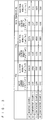
- a sheet carrier density of 0.95 ⁇ 10 13 /cm 2 and an electron mobility of 2174 cm 2 /V ⁇ s are attained at room temperature as shown in the row (a) of Fig. 3.
- the thickness of the second semiconductor layer 6 is 0.5 nm, on the other hand, the result is an electron mobility of 1790 cm 2 /V ⁇ s for a sheet carrier density of 0.95 ⁇ 10 13 /cm 2 at room temperature.
- the second semiconductor layer 6 having a thickness ranging from 0.5 nm to 1.5 nm from the viewpoint of characteristics.
- the increased thickness of the second semiconductor layer 6 presents a problem in that cracks are prone to occur due to a lattice constant difference between the first semiconductor layer 5 and the second semiconductor layer 6.
- the third semiconductor layer 7 is formed of a group-III nitride containing at least Al.
- the third semiconductor layer 7 is formed of a group-III nitride having an Al x Ga 1-x N composition so that the bandgap of the third semiconductor layer 7 is greater than the bandgap of the first semiconductor layer 5.
- the third semiconductor layer 7 has a total thickness ranging from 20 nm to 30 nm in terms of the formation of the two-dimensional electron gas region 5a and the device operation (i.e., the controllability of a main current for gate voltage application).
- the third semiconductor layer 7 is formed by a known deposition technique such as MOCVD and MBE processes.
- the formation of the third semiconductor layer 7 made of a group-III nitride having a higher value of x or an Al-richer group-III nitride produces the greater piezoelectric effect to improve the sheet carrier density in the two-dimensional electron gas region 5a.
- the third semiconductor layer 7 is formed of a group-III nitride which satisfies x ⁇ 0.2. It is, however, necessary to select a growth condition which causes no cracks because the increased value of x is prone to cause cracks.
- the third semiconductor layer 7 is shown as including three layers: a lower layer 7a, an intermediate layer 7b doped with Si as an n-type dopant, and an upper layer 7c.
- the intermediate layer 7b may be doped with an element other than Si instead of Si.
- the intermediate layer 7b functions as a so-called electron supply layer.
- the lower layer 7a functions as a so-called barrier layer, and the upper layer 7c functions as a so-called capping layer.
- the configuration of the third semiconductor layer 7 is not limited to that shown in Fig. 1 if at least the function as the electron supply layer is performed.
- a single electron supply layer may be provided as the third semiconductor layer 7.
- the third semiconductor layer 7 need not be doped with an n-type dopant.
- the third semiconductor layer 7 is preferably formed so that the X-ray rocking curve FWHM for the (002) plane is not greater than 250 seconds, and is also formed so that the pit density at the surface thereof is not greater than 5 ⁇ 10 8 /cm 2 .
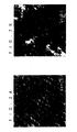
- Fig. 2A illustrates an AFM image of the surface of the semiconductor multilayer structure 1, that is, the surface of the third semiconductor layer 7.
- Fig. 2B illustrates an AFM image of the surface of a semiconductor multilayer structure which does not include the underlying layer 4 for comparison. The former can be said to show fewer pits observed than the latter.
- Such good crystallinity of the third semiconductor layer 7 is by virtue of the appropriate control of the growth conditions of the semiconductor layers depending on the deposition technique to be used in addition to the provision of the underlying layer 4 having the above-mentioned high crystallinity.
- the source electrode 8s and the drain electrode 8d are formed on the surface of the third semiconductor layer 7 (or the upper layer 7c), for example, by Ti/Au/Ni/Au ohmic contact.
- the source electrode 8s and the drain electrode 8d may be formed after a predetermined process for the contact is performed on future electrode portions of the surface of the third semiconductor layer 7.
- the gate electrode 8g is formed on the surface of the third semiconductor layer 7 (or the upper layer 7c), for example, by Pd/Ti/Au Schottky contact.
- the two-dimensional electron gas is formed in the surface of the first semiconductor layer 5 by a piezoelectric effect which forms an electric field extending from the surface to the substrate and a spontaneous polarization effect due to a lattice constant difference between the first semiconductor layer 5 and the second and third semiconductor layers 6, 7.
- the first semiconductor layer 5 is made of GaN free of impurities
- the second semiconductor layer 6 is made of AlN, rather than mixed crystal. This prevents alloy scattering at the heterointerface between the first semiconductor layer 5 and the second semiconductor layer 6 to improve the electron mobility.
- a sheet carrier density of not less than 5 ⁇ 10 12 /cm 2 and an electron mobility of not less than 20000 cm 2 /V ⁇ s at a temperature of 15 K are attained in the HEMT device 2 including the third semiconductor layer 7 made of a group-III nitride having an Al x Ga 1-x N structure where x ⁇ 0.2.
- Japanese Patent Application Laid-Open No. 2004-22577 discloses a HEMT device which includes an electron supply layer having an Al 0.26 Ga 0.74 N composition but does not include a layer corresponding to the second semiconductor layer 6.
- This HEMT device has a sheet carrier density of 1.0 ⁇ 10 13 /cm 2 but has an electron mobility of only 8500 cm 2 /V ⁇ s at a temperature of 15 K.
- the first article by Smorchkova et al. discloses a HEMT device which includes a layer corresponding to the third semiconductor layer 7 made of a group-III nitride having an Al x Ga 1-x N structure where x is greater than 0.25 but does not include a layer corresponding to the underlying layer 4.
- This article does not disclose the characteristic values of the HEMT device at a temperature of 15 K, but discloses the characteristic values at a temperature of 17 K instead.
- This HEMT device has a sheet carrier density of 1.0 ⁇ 10 13 /cm 2 but has an electron mobility of only 6000 cm 2 /V ⁇ s at a temperature of 17 K.
- This article further discloses the characteristic values of a second HEMT device which also does not include a layer corresponding to the second semiconductor layer 6 at a temperature of 17 K.
- the second HEMT device achieves a high sheet carrier density when the compositional limit of the electron supply layer is x ⁇ 0.1.
- the second HEMT device has an electron mobility of only 4000 cm 2 /V ⁇ s although the sheet carrier density is not less than 1.0 ⁇ 10 13 /cm 2 when the compositional limit is x ⁇ 0.2.
- the HEMT device 2 attains a high electron mobility while having a high sheet carrier density as described above even when the HEMT device 2 include the third semiconductor layer 7 having an Al x Ga 1-x N composition where x ⁇ 0.2.
- Such high values of the sheet carrier density and electron mobility far exceed the values easily anticipated from the techniques disclosed in Japanese Patent Application Laid-Open No. 2004-22577 and the first article by Smorchkova et al.
- This preferred embodiment provides the second semiconductor layer 6 between the first semiconductor layer 5 functioning as a channel layer and the third semiconductor layer 7 functioning as the electron supply layer in addition to providing the underlying layer 4 having high crystallinity to improve the crystallinity of the second and third semiconductor layers 6 and 7, from which an inference will be made that this preferred embodiment more effectively suppresses the reduction in electron mobility based on the randomness in arrangement of atoms.
- the above-mentioned very good characteristics are considered to be attained at a temperature of 15 K at which this effect is remarkable.
- the HEMT device 2 including the above-mentioned third semiconductor layer 7 made of the group-III nitride having the Al x Ga 1-x N structure where x ⁇ 0.2 attains a sheet carrier density of not less than 5 ⁇ 10 12 /cm 2 and an electron mobility of not less than 15000 cm 2 /V ⁇ s at a temperature of 77 K, and attains a sheet carrier density of not less than 5 ⁇ 10 12 /cm 2 and an electron mobility of not less than 1900 cm 2 /V ⁇ s at room temperature. Additionally, the transconductance of the HEMT device 2 at room temperature is not less than 150 mS/mm. It can be said that sufficiently increased performance is accomplished in such temperature ranges.
- the HEMT device 2 includes the underlying layer 4 made of the group-III nitride containing at least Al and formed on the substrate 3, and the group of stacked semiconductor layers including the first semiconductor layer 5 made of the group-III nitride, preferably GaN, the second semiconductor layer 6 made of AIN and the third semiconductor layer 7 made of the group-III nitride containing at least Al, preferably Al x Ga 1-x N where x ⁇ 0.2.
- HEMT device The structure of the HEMT device is not limited to that described in the above-mentioned preferred embodiment, but the HEMT device may be of a variety of structures.
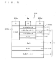
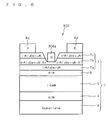
- Figs. 4 through 6 are views showing HEMT devices having structures different from the above-mentioned structure which are prepared using the semiconductor multilayer structure 1 of the preferred embodiment.
- Fig. 4 is a view of a HEMT device 102.
- a process for manufacturing the HEMT device 102 includes etching a portion of the semiconductor multilayer structure 1, for example, by reactive ion etching (RIE) to expose a portion of the first semiconductor layer 5, and then forming a source electrode 108s and a drain electrode 108d.
- RIE reactive ion etching
- Fig. 5 is a view of a HEMT device 202.
- a process for manufacturing the HEMT device 202 includes similarly etching a portion of the semiconductor multilayer structure 1 to expose a portion of the first semiconductor layer 5, providing contact layers 209s and 209d by the selective regrowth of Si-doped GaN, and forming a source electrode 208s and a drain electrode 208d on top of the contact layers 209s and 209d, respectively.
- Fig. 6 is a view of a HEMT device 302.
- the HEMT device 302 includes a tapered groove in a portion (reaching the intermediate layer 7b) of the third semiconductor layer 7 of the semiconductor multilayer structure 1, and a gate electrode 308g on the bottom surface of the tapered groove.
- the HEMT devices having such structures also attain a high electron mobility while maintaining a high sheet carrier density as in the above-mentioned preferred embodiment.
- the semiconductor multilayer structure 1 in the above-mentioned preferred embodiment and the HEMT device 2 employing the semiconductor multilayer structure 1 were prepared.
- a C-plane sapphire single crystal having a diameter of 4 inches and a thickness of 630 ⁇ m was used for the substrate 3, and was placed in a tubular reactor of a predetermined MOCVD apparatus.
- the MOCVD apparatus can supply the tubular reactor with a reaction gas or a carrier gas at least selected from the group consisting of H 2 , N 2 , TMG (trimethylgallium), TMA (trimethylaluminum), NH 3 , and silane gas.
- TMA and hydrogen serving as a TMA carrier gas were supplied, and NH 3 and hydrogen serving as an NH 3 carrier gas were supplied to grow an AIN layer having a thickness of 1 ⁇ m and functioning as the underlying layer 4.
- the X-ray rocking curve FWHM for the (002) plane of the underlying layer 4 thus obtained was 60 seconds.
- the underlying layer 4 thus obtained also had a dislocation density of 1 ⁇ 10 10 /cm 2 and a surface roughness Ra of 0.15 nm.
- the amounts of supply of TMG and NH 3 were set so that the deposition rate was about 3 ⁇ m/hr.
- the temperature was changed to 1080°C.
- TMA and NH 3 were supplied to form an AlN layer having a thickness of 1 nm and functioning as the second semiconductor layer 6.
- the temperature was changed to and held at 1080°C.
- a silane gas was further supplied to dope the third semiconductor layer 7 with Si as an n-type dopant. This formed the lower layer 7a, the Si-doped intermediate layer 7b, and the upper layer 7c having thicknesses of 7 nm, 15 nm and 3 nm, respectively.
- the above-mentioned process steps provided the semiconductor multilayer structure 1.
- the image shown in Fig. 2A was obtained by the AFM observation of the surface of the semiconductor multilayer structure 1 thus obtained, that is, the surface of the third semiconductor layer 7. It is recognized from Fig. 2A that good atomic steps are formed and no cracks are formed in the surface. The pit density at the surface at this time was 5 ⁇ 10 8 /cm 2 .
- the X-ray rocking curve FWHMs for the (002) plane and for the (102) plane were 203 seconds and 370 seconds, respectively. It was recognized from these facts that the semiconductor multilayer structure 1 had good surface quality.
- the Ti/Au/Ni/Au source and drain electrodes 8s and 8d were formed by ohmic contact in predetermined positions of the surface of the semiconductor multilayer structure 1, and the Pd/Ti/Au gate electrode 8g was formed by Schottky contact, whereby the HEMT device 2 was obtained.
- Results of measurement of the sheet carrier density and the electron mobility for the HEMT device 2 thus obtained at a temperature of 15 K, at a temperature of 77K and at room temperature are shown in the row (a) of Fig. 3.
- a high electron mobility exceeding 25000 cm 2 /V ⁇ s is attained at the temperature of 15 K while a sheet carrier density close to 1.0 ⁇ 10 13 /cm 2 is maintained.
- the transconductance was 160 mS/mm at room temperature when the gate length was 2 ⁇ m.
- a HEMT device identical in semiconductor multilayer structure with the HEMT device 2 of Inventive Example except for the absence of the underlying layer 4 was prepared as Comparative Example 1.
- the image shown in Fig. 2B was obtained by the AFM observation of the surface of the semiconductor multilayer structure thus obtained, that is, the surface of the third semiconductor layer. Black spots indicating pits are found everywhere in the image of Fig. 2B, and it is recognized that the unevenness of the surface in Fig. 2B is greater than that in Inventive Example shown in Fig. 2A.
- the pit density at the surface at this time was about 2 ⁇ 10 10 /cm 2 .
- the X-ray rocking curve FWHMs for the (002) plane and for the (102) plane were 319 seconds and 795 seconds, respectively. It is therefore understood that the semiconductor multilayer structure in Comparative Example 1 is inferior in crystallinity to that in Inventive Example.
- a HEMT device identical in semiconductor multilayer structure with the HEMT device 2 of Inventive Example except for the absence of the second semiconductor layer 6 was prepared as Comparative Example 2.
- a HEMT device identical in semiconductor multilayer structure with the HEMT device of Inventive Example except for the absence of the underlying layer 4 and the second semiconductor layer 6 was prepared as Comparative Example 3.
- the HEMT device attains a high electron mobility while having a high sheet carrier density even when the HEMT device includes an electron supply layer having an Al x Ga 1-x N composition where x ⁇ 0.2, and in particular has a more remarkably excellent characteristic which is not less than three times that of Comparative Examples at a temperature of 15 K.
- a semiconductor device includes an underlying layer made of a group-III nitride containing at least Al and formed on a substrate, and a group of stacked semiconductor layers including a first semiconductor layer made of a group-III nitride, preferably GaN, a second semiconductor layer made of AlN and a third semiconductor layer made of a group-III nitride containing at least Al, preferably Al x Ga 1-x N where x ⁇ 0.2.
- the semiconductor device suppresses the reduction in electron mobility resulting from lattice defects and crystal lattice randomness. This achieves a HEMT device having a sheet carrier density of not less than 1 ⁇ 10 13 /cm 2 and an electron mobility of not less than 20000 cm 2 /V ⁇ s at a temperature of 15 K.
Landscapes
- Junction Field-Effect Transistors (AREA)
Abstract
Description
- The present invention relates to a HEMT (High Electron Mobility Transistor) employing a group-III nitride.
- Group-III nitride semiconductors including GaN, because of their large bandgap, high breakdown field strength and high melting point, have been expected as high-power, high-frequency and high-temperature semiconductor device materials alternative to GaAs-based materials. HEMTs (High Electron Mobility Transistors) and the like have been studied and developed as devices which take advantage of such physical properties. An example of the HEMTs having been studied and developed is a heterostructure HEMT including a substrate made of sapphire, SiC or the like, a GaN channel layer formed on the substrate, and a so-called electron supply layer of AlGaN or AIN formed on the channel layer.
- In a HEMT as described above, a two-dimensional electron gas is formed at the surface of the channel layer by a piezoelectric effect such that an electric field extending from the surface to the substrate is formed and by a spontaneous polarization effect due to an (a-axis) lattice constant difference between the channel layer and the electron supply layer. The Al-richer the AlGaN layer is, the greater the lattice constant difference becomes, and the piezoelectric effect and the spontaneous polarization effect increase accordingly.
- For increase in performance of the HEMT, there is a need to enhance electron mobility while maintaining a high carrier density (or sheet carrier density) at the surface of the channel layer. Attempts to satisfy the need by devising the structure of the HEMT device have been known. (See, for example, Japanese Patent Application Laid-Open No. 2004-22577; Smorchkova et al., "AlN/GaN and (Al,Ga)N/AlN/GaN two-dimensional electron gas structures grown by plasma-assisted molecular-beam epitaxy," Journal of Applied Physics, Volume 90, Number 10, pp. 5196-5201; Smorchkova et al., "AlGaN/AlN/GaN High-Power Microwave HEMT," IEEE Electron Device Letters, Vol. 22, No. 10, pp. 457-459.)
- There are a variety of electron scattering mechanisms that influence the electron mobility for semiconductor. The electron scattering mechanisms are roughly classified into a mechanism based on lattice vibrations and a mechanism based on the randomness in arrangement of atoms. The former is caused by thermal energy, has a temperature dependence, and hardly contributes to the reduction in electron mobility at cryogenic temperatures. The latter, on the other hand, is caused by the presence of lattice defects and impurities, and differs from the former in that the influence of the randomness in arrangement of atoms still remains even at cryogenic temperatures. Thus, the enhancement in electron mobility at cryogenic temperatures means the reduction in the influence of the randomness in arrangement of atoms upon the electron mobility.
- Japanese Patent Application Laid-Open No. 2004-22577 discloses a technique of providing a highly crystalline underlying layer containing AIN at an interface between a substrate and a GaN layer in a HEMT having an Al0.26Ga0.74N/GaN heterostructure to improve the crystallinity of a channel layer and an electron supply layer which are formed on the underlying layer, thereby increasing the performance of the HEMT. This technique achieves the HEMT having a sheet carrier density of 1×10¹³ /cm2 or higher and an electron mobility of 8000 cm2 /V·s or higher at a temperature of 15 K.
- The first article by Smorchkova et al., on the other hand, discloses a HEMT having an AlxGa1-xN/AlN/GaN structure in which an AIN layer is inserted at the interface of an AIGaN/GaN heterostructure for the purpose of avoiding alloy disorder scattering which is one of the scattering mechanisms resulting from the randomness in arrangement of atoms. This HEMT has a sheet carrier density of about 1.4 × 10¹³ /cm2 or higher and an electron mobility of 4000 cm2/V·s at a temperature of 17 K when x ranges from 0.25 to 0.45. Also, a HEMT having an AlxGa1-xN/GaN structure in which AlN is not inserted is achieved. This HEMT has an electron mobility exceeding 15000 cm2/V·s when x is less than 0.2, in which case, however, the sheet carrier density is less than 5×10¹²/cm2.
- The present invention is intended for a semiconductor device employing a group-III nitride, and a HEMT (High Electron Mobility Transistor) including the semiconductor device.
- According to the present invention, the semiconductor device comprises: a predetermined base; an underlying layer formed on the base; and a group of semiconductor layers formed on the underlying layer and including a first semiconductor layer made of a first group-III nitride, a second semiconductor layer made of AIN which is a second group-III nitride, and a third semiconductor layer made of a third group-III nitride containing at least Al, the first, second and third semiconductor layers being stacked together in the order named as seen from the underlying layer side, the underlying layer being made of a fourth group-III nitride containing at least Al and having a higher Al mole fraction in all of the group-III elements than does the first group-III nitride, the semiconductor device having a sheet carrier density of not less than 5×10¹² /cm2 and an electron mobility of not less than 20000 cm2/V·s at a temperature of 15 K.
- This provides the semiconductor device having a good device characteristic, or a HEMT device including the semiconductor device. In particular, the attainment of the good device characteristic at cryogenic temperatures at which scattering factors have a little influence resulting from lattice vibrations achieves the provision of the semiconductor device and the like suppressing the reduction in electron mobility resulting from lattice defects and crystal lattice randomness.
- Preferably, the underlying layer has a dislocation density of not greater than 1×10¹¹ /cm2.
- The formation of the group of semiconductor layers over the underlying layer having such good crystal quality provides the good crystal quality of the group of semiconductor layers to achieve the semiconductor device having a high electron mobility.
- More preferably, the fourth group-III nitride has an Al mole fraction of not less than 50 atom percent in all of the group-III elements.
- The formation of the underlying layer made of such an Al-rich group-III nitride easily achieves the good crystal quality of the underlying layer.
- It is therefore an object of the present invention to provide a semiconductor device and the like suppressing the reduction in electron mobility resulting from lattice defects and crystal lattice randomness and attaining a high electron mobility while maintaining a high sheet carrier density.
- These and other objects, features, aspects and advantages of the present invention will become more apparent from the following detailed description of the present invention when taken in conjunction with the accompanying drawings.
-
- Fig. 1 is a schematic view showing the construction of a HEMT device formed by employing a semiconductor multilayer structure according to the present invention;
- Figs. 2A and 2B show AFM images of the surface of the semiconductor multilayer structure;
- Fig. 3 shows a table providing a listing of values of a sheet carrier density and an electron mobility for HEMT devices in Inventive Example and Comparative Examples; and
- Figs. 4 through 6 are schematic views showing the constructions of HEMT devices according to modifications of the present invention.
-
- Fig. 1 is a schematic view showing the construction of a
HEMT device 2 formed by employing asemiconductor multilayer structure 1 according to a preferred embodiment of the present invention. For purposes of illustration, the thicknesses of respective layers shown in Fig. 1 are not drawn to scale. - The
semiconductor multilayer structure 1 includes anunderlying layer 4, afirst semiconductor layer 5, asecond semiconductor layer 6 and athird semiconductor layer 7 which are formed on a substrate (base) 3. Thefirst semiconductor layer 5, thesecond semiconductor layer 6 and thethird semiconductor layer 7 are also generically referred to simply as semiconductor layers or a group of semiconductor layers hereinafter. Thesemiconductor multilayer structure 1 is also referred to hereinafter as an epitaxial substrate because thesemiconductor multilayer structure 1 is formed by epitaxially growing the group of semiconductor layers on thesubstrate 3 and is provided for the subsequent device formation in a manner similar to a substrate, as will be described hereinbelow. - The HEMT
device 2 includes a source electrode 8s, adrain electrode 8d and agate electrode 8g which are formed on thesemiconductor multilayer structure 1. - The material of the
substrate 3 is appropriately selected in accordance with the composition and structure of theunderlying layer 4 and semiconductor layers to be formed thereon or the technique of forming the layers. For example, a single crystal of SiC (silicon carbide) or sapphire cut to a predetermined thickness is used for thesubstrate 3. Alternatively, the material of thesubstrate 3 may be appropriately selected from the group consisting of: oxide materials such as ZnO, LiAlO2, LiGaO2, MgAl2O4, (LaSr)(AlTa)O3, NdGaO3 and MgO; group-IV single crystals such as Si and Ge; IV-IV compounds such as SiGe; III-V compounds such as GaAs, AlN, GaN and AIGaN; and single crystals of borides such as ZrB2. Of such single crystals, an SiC substrate or a sapphire substrate is desirable. In particular, when a group-III nitride layer having a main surface coincident with the C plane thereof is provided as theunderlying layer 4, it is desirable to use C-plane SiC or C-plane sapphire as the material of thesubstrate 3. This is because the use of such materials achieves the formation of theunderlying layer 4 of high quality. When a group-III nitride layer having a main surface coincident with the A plane thereof is provided as theunderlying layer 4, it is desirable to use A-plane SiC or R-plane sapphire as the material of thesubstrate 3. There are no special material limitations on the thickness of thesubstrate 3, but thesubstrate 3 having a thickness ranging from hundreds of micrometers to several millimeters are preferable for convenience of handling. - The
underlying layer 4 is formed of a group-III nitride containing at least aluminum (Al) and having a higher Al mole fraction in all of the group-III elements than does the group-III nitride constituting the first semiconductor layer 5 (to be described later). Preferably, theunderlying layer 4 is formed of a group-III nitride having an Al mole fraction in all of the group-III elements which is not less than 50 atom percent. More preferably, theunderlying layer 4 is formed of a group-III nitride having an Al mole fraction in all of the group-III elements which is not less than 80 atom percent. Most preferably, theunderlying layer 4 is formed of AlN. Theunderlying layer 4 is made of the group-III nitride of the above-mentioned composition because the threading dislocations from theunderlying layer 4 are tangled with each other by the action of a substantially horizontal compressive stress produced near an interface portion of thefirst semiconductor layer 5 with theunderlying layer 4 to consequently produce the effect of reducing the dislocations in thefirst semiconductor layer 5. The greater the difference in Al mole fraction between theunderlying layer 4 and thefirst semiconductor layer 5 is, the greater the effect of reducing the dislocations is. This effect is maximized when theunderlying layer 4 is made of AlN. It is, however, ascertained in experiments that the use of the group-III nitride having an Al mole fraction in all of the group-III elements which is not less than 80 atom percent as the material of theunderlying layer 4 is as effective in reducing the dislocations as the use of AlN. The use of AIN as the material of theunderlying layer 4 has another advantage that variations in composition do not present a problem. Theunderlying layer 4 is illustrated in Fig. 1 as made of AlN. - The
underlying layer 4 thus formed typically takes on a hexagonal wurtzite structure. In particular, when a group-III nitride layer having a main surface coincident with the C plane thereof is used as the material of theunderlying layer 4, the FWHM (full width at half maximum) for the (002) plane by X-ray rocking curve measurement (ω scan) for theunderlying layer 4 is preferably not greater than 200 seconds, and more preferably not greater than 100 seconds. The attainment of such an FWHM means small fluctuations in growth orientation, aligned C planes and reduced dislocations of spiral components at the surface of theunderlying layer 4. This is more preferable in forming thefirst semiconductor layer 5 of good crystal quality on theunderlying layer 4. To achieve such crystallinity, it is not desirable to insert a so-called low-temperature buffer layer on thebase 3. The lower limit of the FWHM for the (002) plane by the X-ray rocking curve measurement (ω scan) is not particularly determined, but does not fall below a theoretical value (10 seconds or lower) calculated from the material and crystal structure. It is desirable that the edge dislocation density in theunderlying layer 4 be not greater than 5 × 10¹⁰ /cm2. This condition can be achieved by forming a nitride layer on the surface of thesubstrate 3. Depending on the condition settings, the edge dislocation density as low as 1 × 10⁹ /cm2 is attainable. In this preferred embodiment, the dislocation density is evaluated by using plan view TEM. - The
underlying layer 4 preferably has a thickness ranging from 10 nm to 100 µm. The thickness lower than the above range is not preferable because insufficient crystal growth occurs in theunderlying layer 4 and most of the many dislocations produced at the interface between thesubstrate 3 and theunderlying layer 4 remain in the surface of theunderlying layer 4. It is therefore desirable to form theunderlying layer 4 having at least such a thickness that a dislocation density of not greater than 5×10¹⁰/cm2 is attained for the purpose of sufficiently eliminating the internal dislocations. Theunderlying layer 4 having a thickness of not less than 300 nm can attain a dislocation density of not greater than 5×10¹⁰/cm2 with stability. An excessive thickness, however, presents a disadvantage in costs and creates a likelihood that cracks are formed within theunderlying layer 4. Thus, the thickness of theunderlying layer 4 is appropriately defined within a range in which the formation of cracks is prevented. It is desirable that the thickness of theunderlying layer 4 be not greater than 10 µm. - The
underlying layer 4 may be formed, for example, by using an MOCVD process or an MBE (Molecular Beam Epitaxy) process. The MOCVD process may be used in combination with a PALE (Pulsed Atomic Layer Epitaxy) process, a plasma assisted process or a laser assisted process. The MBE process may also be used in combination with similar techniques. The growth methods such as the MOCVD process and the MBE process, which are capable of controlling the manufacturing conditions with high accuracy, are suitable for the growth of high-quality crystals. The use of such methods capable of setting reduced-pressure conditions at a heating temperature of 1100°C to 1600°C is desirable for the growth of the high-qualityunderlying layer 4 of AIN on a dissimilar base. More specific preparation conditions will be suitably selected and set in accordance with the above-mentioned growth techniques. Of these methods, it is especially desirable to use the MOCVD process which can achieve a state approaching a state of thermal equilibrium. - It is desirable that the topmost surface of the
underlying layer 4 be substantially flat at the atomic level. In this case, the surface of theunderlying layer 4 has such flatness that an atomic step is clearly observed, and the surface roughness (evaluated herein by using arithmetic mean roughness Ra in a 5- by 5-µm square region) of the topmost surface evaluated based on an AFM (Atomic Force Microscope) image is not greater than 0.5 nm which is approximately equal to the c-axis lattice constant of the group-III nitride material constituting theunderlying layer 4, and preferably not greater than 0.3 nm. Few pits are observed at the surface when the value of the arithmetic mean roughness Ra is not greater than 0.3 nm. - To achieve such flatness of the surface of the
underlying layer 4 at the atomic level, it is preferable to use a crystal growth technique which makes it difficult to cause variations in local unevenness. The MOCVD process in which a growth rate is several micrometers per hour at the most can be said to be preferred as the crystal growth technique. To form theunderlying layer 4 as described above by the MOCVD process using trimethylaluminum and ammonia, it is desirable that the temperature of the substrate itself range from 1100°C to 1250°C; the pressure during the growth range from 5 Torr to 20 Torr; and a supply ratio between trimethylaluminum and ammonia be not greater than 1:500, more preferably not greater than 1:200. - The
first semiconductor layer 5 is preferably formed of a high-resistance group-III nitride. More preferably, thefirst semiconductor layer 5 is formed of GaN (i-GaN) free of impurities which become a factor responsible for reductions in resistance. Thefirst semiconductor layer 5 is illustrated in Fig. 1 as made of i-GaN. Thefirst semiconductor layer 5 is also formed by a known deposition technique such as MOCVD and MBE processes. Thefirst semiconductor layer 5 also has good crystal quality because thefirst semiconductor layer 5 is formed on theunderlying layer 4 having high crystallinity as described above. - The higher the surface flatness of the
underlying layer 4 is, the more effectively the above-mentioned dislocation reduction effect in thefirst semiconductor layer 5 is produced. The internal dislocation density of thefirst semiconductor layer 5 can be not greater than one-half the dislocation density of at least the surface portion of theunderlying layer 4, and can be reduced to 5×10⁷ /cm2. The formation of thefirst semiconductor layer 5 on theunderlying layer 4 flat to such a degree that few pits exist on the surface improves the surface flatness of thethird semiconductor layer 7 in addition to being able to suppress the occurrence of a situation such that crystal defects are induced by the pits in thefirst semiconductor layer 5. - A two-dimensional
electron gas region 5a produced by a high-concentration two-dimensional electron gas is formed near the upper surface of thefirst semiconductor layer 5 by supplying electrons serving as carriers from thethird semiconductor layer 7. For this reason, thefirst semiconductor layer 5 is required to have a thickness large enough to ensure the two-dimensionalelectron gas region 5a. It is, however, preferable to form thefirst semiconductor layer 5 having a thickness of about several micrometers because an excessive thickness is prone to cause cracks. - The
second semiconductor layer 6 is formed of AlN. Thesecond semiconductor layer 6 preferably has a thickness of not greater than 5 nm. When the thickness of thesecond semiconductor layer 6 is 1 nm, a sheet carrier density of 0.95×10¹³ /cm2 and an electron mobility of 2174 cm2/V·s are attained at room temperature as shown in the row (a) of Fig. 3. When the thickness of thesecond semiconductor layer 6 is 0.5 nm, on the other hand, the result is an electron mobility of 1790 cm2/V·s for a sheet carrier density of 0.95×10¹³ /cm2 at room temperature. Considering these results, it is more preferable to form thesecond semiconductor layer 6 having a thickness ranging from 0.5 nm to 1.5 nm from the viewpoint of characteristics. The increased thickness of thesecond semiconductor layer 6 presents a problem in that cracks are prone to occur due to a lattice constant difference between thefirst semiconductor layer 5 and thesecond semiconductor layer 6. - The
third semiconductor layer 7 is formed of a group-III nitride containing at least Al. Preferably, thethird semiconductor layer 7 is formed of a group-III nitride having an AlxGa1-xN composition so that the bandgap of thethird semiconductor layer 7 is greater than the bandgap of thefirst semiconductor layer 5. Preferably, thethird semiconductor layer 7 has a total thickness ranging from 20 nm to 30 nm in terms of the formation of the two-dimensionalelectron gas region 5a and the device operation (i.e., the controllability of a main current for gate voltage application). - The
third semiconductor layer 7 is formed by a known deposition technique such as MOCVD and MBE processes. The formation of thethird semiconductor layer 7 made of a group-III nitride having a higher value of x or an Al-richer group-III nitride produces the greater piezoelectric effect to improve the sheet carrier density in the two-dimensionalelectron gas region 5a. Preferably, thethird semiconductor layer 7 is formed of a group-III nitride which satisfies x ≥ 0.2. It is, however, necessary to select a growth condition which causes no cracks because the increased value of x is prone to cause cracks. - Referring to Fig. 1, the
third semiconductor layer 7 is shown as including three layers: alower layer 7a, anintermediate layer 7b doped with Si as an n-type dopant, and anupper layer 7c. Theintermediate layer 7b may be doped with an element other than Si instead of Si. In the instance shown in Fig. 1, theintermediate layer 7b functions as a so-called electron supply layer. Thelower layer 7a functions as a so-called barrier layer, and theupper layer 7c functions as a so-called capping layer. The configuration of thethird semiconductor layer 7 is not limited to that shown in Fig. 1 if at least the function as the electron supply layer is performed. For example, a single electron supply layer may be provided as thethird semiconductor layer 7. Further, thethird semiconductor layer 7 need not be doped with an n-type dopant. - The
third semiconductor layer 7 is preferably formed so that the X-ray rocking curve FWHM for the (002) plane is not greater than 250 seconds, and is also formed so that the pit density at the surface thereof is not greater than 5 × 10⁸ /cm2. Fig. 2A illustrates an AFM image of the surface of thesemiconductor multilayer structure 1, that is, the surface of thethird semiconductor layer 7. Fig. 2B illustrates an AFM image of the surface of a semiconductor multilayer structure which does not include theunderlying layer 4 for comparison. The former can be said to show fewer pits observed than the latter. Such good crystallinity of thethird semiconductor layer 7 is by virtue of the appropriate control of the growth conditions of the semiconductor layers depending on the deposition technique to be used in addition to the provision of theunderlying layer 4 having the above-mentioned high crystallinity. - The source electrode 8s and the
drain electrode 8d are formed on the surface of the third semiconductor layer 7 (or theupper layer 7c), for example, by Ti/Au/Ni/Au ohmic contact. The source electrode 8s and thedrain electrode 8d may be formed after a predetermined process for the contact is performed on future electrode portions of the surface of thethird semiconductor layer 7. Thegate electrode 8g is formed on the surface of the third semiconductor layer 7 (or theupper layer 7c), for example, by Pd/Ti/Au Schottky contact. - In the
HEMT device 2 having such a construction, the two-dimensional electron gas is formed in the surface of thefirst semiconductor layer 5 by a piezoelectric effect which forms an electric field extending from the surface to the substrate and a spontaneous polarization effect due to a lattice constant difference between thefirst semiconductor layer 5 and the second andthird semiconductor layers first semiconductor layer 5 is made of GaN free of impurities, and thesecond semiconductor layer 6 is made of AlN, rather than mixed crystal. This prevents alloy scattering at the heterointerface between thefirst semiconductor layer 5 and thesecond semiconductor layer 6 to improve the electron mobility. - For example, a sheet carrier density of not less than 5×10¹² /cm2 and an electron mobility of not less than 20000 cm2/V·s at a temperature of 15 K are attained in the
HEMT device 2 including thethird semiconductor layer 7 made of a group-III nitride having an AlxGa1-xN structure where x ≥ 0.2. - Japanese Patent Application Laid-Open No. 2004-22577 discloses a HEMT device which includes an electron supply layer having an Al0.26Ga0.74N composition but does not include a layer corresponding to the
second semiconductor layer 6. This HEMT device has a sheet carrier density of 1.0×10¹³ /cm2 but has an electron mobility of only 8500 cm2/V·s at a temperature of 15 K. - The first article by Smorchkova et al. discloses a HEMT device which includes a layer corresponding to the
third semiconductor layer 7 made of a group-III nitride having an AlxGa1-xN structure where x is greater than 0.25 but does not include a layer corresponding to theunderlying layer 4. This article does not disclose the characteristic values of the HEMT device at a temperature of 15 K, but discloses the characteristic values at a temperature of 17 K instead. This HEMT device has a sheet carrier density of 1.0×10¹³ /cm2 but has an electron mobility of only 6000 cm2 /V·s at a temperature of 17 K. This article further discloses the characteristic values of a second HEMT device which also does not include a layer corresponding to thesecond semiconductor layer 6 at a temperature of 17 K. The second HEMT device achieves a high sheet carrier density when the compositional limit of the electron supply layer is x < 0.1. The second HEMT device, however, has an electron mobility of only 4000 cm2/V·s although the sheet carrier density is not less than 1.0 × 10¹³ /cm2 when the compositional limit is x ≥ 0.2. - The
HEMT device 2 according to this preferred embodiment, on the other hand, attains a high electron mobility while having a high sheet carrier density as described above even when theHEMT device 2 include thethird semiconductor layer 7 having an AlxGa1-xN composition where x ≥ 0.2. Such high values of the sheet carrier density and electron mobility far exceed the values easily anticipated from the techniques disclosed in Japanese Patent Application Laid-Open No. 2004-22577 and the first article by Smorchkova et al. This preferred embodiment provides thesecond semiconductor layer 6 between thefirst semiconductor layer 5 functioning as a channel layer and thethird semiconductor layer 7 functioning as the electron supply layer in addition to providing theunderlying layer 4 having high crystallinity to improve the crystallinity of the second andthird semiconductor layers - Further, the
HEMT device 2 including the above-mentionedthird semiconductor layer 7 made of the group-III nitride having the AlxGa1-xN structure where x ≥ 0.2 attains a sheet carrier density of not less than 5×10¹² /cm2 and an electron mobility of not less than 15000 cm2/V·s at a temperature of 77 K, and attains a sheet carrier density of not less than 5×10¹² /cm2 and an electron mobility of not less than 1900 cm2/V·s at room temperature. Additionally, the transconductance of theHEMT device 2 at room temperature is not less than 150 mS/mm. It can be said that sufficiently increased performance is accomplished in such temperature ranges. - As described hereinabove, the
HEMT device 2 according to this preferred embodiment includes theunderlying layer 4 made of the group-III nitride containing at least Al and formed on thesubstrate 3, and the group of stacked semiconductor layers including thefirst semiconductor layer 5 made of the group-III nitride, preferably GaN, thesecond semiconductor layer 6 made of AIN and thethird semiconductor layer 7 made of the group-III nitride containing at least Al, preferably AlxGa1-xN where x ≥ 0.2. This suppresses the reduction electron mobility resulting from lattice defects and crystal lattice randomness to attain a high electron mobility while maintaining a high sheet carrier density. - The structure of the HEMT device is not limited to that described in the above-mentioned preferred embodiment, but the HEMT device may be of a variety of structures. Figs. 4 through 6 are views showing HEMT devices having structures different from the above-mentioned structure which are prepared using the
semiconductor multilayer structure 1 of the preferred embodiment. - Fig. 4 is a view of a
HEMT device 102. A process for manufacturing theHEMT device 102 includes etching a portion of thesemiconductor multilayer structure 1, for example, by reactive ion etching (RIE) to expose a portion of thefirst semiconductor layer 5, and then forming a source electrode 108s and adrain electrode 108d. - Fig. 5 is a view of a
HEMT device 202. A process for manufacturing theHEMT device 202 includes similarly etching a portion of thesemiconductor multilayer structure 1 to expose a portion of thefirst semiconductor layer 5, providingcontact layers drain electrode 208d on top of the contact layers 209s and 209d, respectively. - Fig. 6 is a view of a
HEMT device 302. TheHEMT device 302 includes a tapered groove in a portion (reaching theintermediate layer 7b) of thethird semiconductor layer 7 of thesemiconductor multilayer structure 1, and agate electrode 308g on the bottom surface of the tapered groove. - The HEMT devices having such structures also attain a high electron mobility while maintaining a high sheet carrier density as in the above-mentioned preferred embodiment.
- In Inventive Example, the
semiconductor multilayer structure 1 in the above-mentioned preferred embodiment and theHEMT device 2 employing thesemiconductor multilayer structure 1 were prepared. For the preparation of thesemiconductor multilayer structure 1, a C-plane sapphire single crystal having a diameter of 4 inches and a thickness of 630 µm was used for thesubstrate 3, and was placed in a tubular reactor of a predetermined MOCVD apparatus. The MOCVD apparatus can supply the tubular reactor with a reaction gas or a carrier gas at least selected from the group consisting of H2, N2, TMG (trimethylgallium), TMA (trimethylaluminum), NH3, and silane gas. While a carrier gas of hydrogen flowed at a flow rate of 3 m/sec and the pressure within the tubular reactor was maintained at 20 Torr, the temperature of thesubstrate 3 was raised up to 1200°C and thereafter held at 1200°C for ten minutes. Thus, thermal cleaning was performed on thesubstrate 3. - Thereafter, while the substrate temperature was held at 1200°C, TMA and hydrogen serving as a TMA carrier gas were supplied, and NH3 and hydrogen serving as an NH3 carrier gas were supplied to grow an AIN layer having a thickness of 1 µm and functioning as the
underlying layer 4. In this process step, the flow rates of TMA and NH3 were controlled so that the supply molar ratio therebetween satisfied TMA:NH3 = 1:450. The X-ray rocking curve FWHM for the (002) plane of theunderlying layer 4 thus obtained was 60 seconds. Theunderlying layer 4 thus obtained also had a dislocation density of 1 × 10¹⁰ /cm2 and a surface roughness Ra of 0.15 nm. - Subsequently, after the temperature and the pressure were changed to and held at 1100°C and 760 Torr respectively, TMG and NH3 were supplied so that the supply molar ratio therebetween satisfied TMG:NH3 = 1:2000 to form a GaN layer having a thickness of 2 µm and functioning as the
first semiconductor layer 5. In this process step, the amounts of supply of TMG and NH3 were set so that the deposition rate was about 3 µm/hr. - After the formation of the GaN layer, the temperature was changed to 1080°C. Then, TMA and NH3 were supplied to form an AlN layer having a thickness of 1 nm and functioning as the
second semiconductor layer 6. In this process step, TMA and NH3 were supplied so that the supply molar ratio therebetween satisfied TMA:NH3 = 1:450. - After the formation of the AIN layer, the temperature was changed to and held at 1080°C. Then, TMA, TMG and NH3 were supplied so that the supply molar ratio therebetween satisfied TMA:TMG:NH3 = 0.2:0.7:2000 to form the
third semiconductor layer 7 having an Al0.26Ga0.74N composition. In the course of this process step, a silane gas was further supplied to dope thethird semiconductor layer 7 with Si as an n-type dopant. This formed thelower layer 7a, the Si-dopedintermediate layer 7b, and theupper layer 7c having thicknesses of 7 nm, 15 nm and 3 nm, respectively. The above-mentioned process steps provided thesemiconductor multilayer structure 1. - The image shown in Fig. 2A was obtained by the AFM observation of the surface of the
semiconductor multilayer structure 1 thus obtained, that is, the surface of thethird semiconductor layer 7. It is recognized from Fig. 2A that good atomic steps are formed and no cracks are formed in the surface. The pit density at the surface at this time was 5×10⁸ /cm2. The X-ray rocking curve FWHMs for the (002) plane and for the (102) plane were 203 seconds and 370 seconds, respectively. It was recognized from these facts that thesemiconductor multilayer structure 1 had good surface quality. - The Ti/Au/Ni/Au source and
drain electrodes 8s and 8d were formed by ohmic contact in predetermined positions of the surface of thesemiconductor multilayer structure 1, and the Pd/Ti/Au gate electrode 8g was formed by Schottky contact, whereby theHEMT device 2 was obtained. - Results of measurement of the sheet carrier density and the electron mobility for the
HEMT device 2 thus obtained at a temperature of 15 K, at a temperature of 77K and at room temperature are shown in the row (a) of Fig. 3. In particular, a high electron mobility exceeding 25000 cm2/V·s is attained at the temperature of 15 K while a sheet carrier density close to 1.0×10¹³ /cm2 is maintained. The transconductance was 160 mS/mm at room temperature when the gate length was 2 µm. - A HEMT device identical in semiconductor multilayer structure with the
HEMT device 2 of Inventive Example except for the absence of theunderlying layer 4 was prepared as Comparative Example 1. - The image shown in Fig. 2B was obtained by the AFM observation of the surface of the semiconductor multilayer structure thus obtained, that is, the surface of the third semiconductor layer. Black spots indicating pits are found everywhere in the image of Fig. 2B, and it is recognized that the unevenness of the surface in Fig. 2B is greater than that in Inventive Example shown in Fig. 2A. The pit density at the surface at this time was about 2×10¹⁰ /cm2. The X-ray rocking curve FWHMs for the (002) plane and for the (102) plane were 319 seconds and 795 seconds, respectively. It is therefore understood that the semiconductor multilayer structure in Comparative Example 1 is inferior in crystallinity to that in Inventive Example.
- Results of measurement of the sheet carrier density and the electron mobility for the HEMT device thus obtained at a temperature of 15 K, at a temperature of 77K and at room temperature are shown in the row (b) of Fig. 3. At the temperature of 15 K, the sheet carrier density of Comparative Example 1 was comparable to that of Inventive Example, but the electron mobility of Comparative Example 1 was only 8000 cm2 /V·s. The transconductance was 130 mS/mm at room temperature when the gate length was 2 µm.
- A HEMT device identical in semiconductor multilayer structure with the
HEMT device 2 of Inventive Example except for the absence of thesecond semiconductor layer 6 was prepared as Comparative Example 2. - Results of measurement of the sheet carrier density and the electron mobility for the HEMT device thus obtained at a temperature of 15 K, at a temperature of 77K and at room temperature are shown in the row (c) of Fig. 3. At the temperature of 15 K, the sheet carrier density of Comparative Example 2 was comparable to that of Inventive Example, but the electron mobility of Comparative Example 2 was only 5000 cm2/V·s. The transconductance was 130 mS/mm at room temperature when the gate length was 2 µm.
- A HEMT device identical in semiconductor multilayer structure with the HEMT device of Inventive Example except for the absence of the
underlying layer 4 and thesecond semiconductor layer 6 was prepared as Comparative Example 3. - Results of measurement of the sheet carrier density and the electron mobility for the HEMT device thus obtained at a temperature of 15 K, at a temperature of 77K and at room temperature are shown in the row (d) of Fig. 3. At the temperature of 15 K, the sheet carrier density of Comparative Example 3 was comparable to that of Inventive Example, but the electron mobility of Comparative Example 3 was only 4000 cm2 / V·s. The transconductance was 120 mS/mm at room temperature when the gate length was 2 µm.
- It will be found from Inventive Example and Comparative Examples 1 to 3 described above that the HEMT device according to the preferred embodiment attains a high electron mobility while having a high sheet carrier density even when the HEMT device includes an electron supply layer having an AlxGa1-xN composition where x ≥ 0.2, and in particular has a more remarkably excellent characteristic which is not less than three times that of Comparative Examples at a temperature of 15 K.
- While the invention has been described in detail, the foregoing description is in all aspects illustrative and not restrictive. It is understood that numerous other modifications and variations can be devised without departing from the scope of the invention.
- A semiconductor device includes an underlying layer made of a group-III nitride containing at least Al and formed on a substrate, and a group of stacked semiconductor layers including a first semiconductor layer made of a group-III nitride, preferably GaN, a second semiconductor layer made of AlN and a third semiconductor layer made of a group-III nitride containing at least Al, preferably AlxGa1-xN where x ≥ 0.2. The semiconductor device suppresses the reduction in electron mobility resulting from lattice defects and crystal lattice randomness..This achieves a HEMT device having a sheet carrier density of not less than 1×10¹³ /cm2 and an electron mobility of not less than 20000 cm2 /V·s at a temperature of 15 K.
Claims (16)
- A semiconductor multilayer structure comprising:said first, second and third semiconductor layers being stacked together in the order named as seen from the underlying layer side,a predetermined base;an underlying layer formed on said base; anda group of semiconductor layers formed on said underlying layer and includinga first semiconductor layer made of a first group-III nitride,a second semiconductor layer made of AlN which is a second group-III nitride, anda third semiconductor layer made of a third group-III nitride containing at least Al,
said underlying layer being made of a fourth group-III nitride containing at least Al and having a higher Al mole fraction in all of the group-III elements than does said first group-III nitride,
said semiconductor multilayer structure having a sheet carrier density of not less than 5×10¹² /cm2 and an electron mobility of not less than 20000 cm2/V·s at a temperature of 15 K. - A semiconductor device comprising:said first, second and third semiconductor layers being stacked together in the order named as seen from the underlying layer side,a predetermined base;an underlying layer formed on said base; anda group of semiconductor layers formed on said underlying layer and includinga first semiconductor layer made of a first group-III nitride,a second semiconductor layer made of AlN which is a second group-III nitride, anda third semiconductor layer made of a third group-III nitride containing at least Al,
said underlying layer being made of a fourth group-III nitride containing at least Al and having a higher Al mole fraction in all of the group-III elements than does said first group-III nitride,
said semiconductor device having a sheet carrier density of not less than 5 × 10¹² /cm2 and an electron mobility of not less than 20000 cm2 /V·s at a temperature of 15 K. - The semiconductor device according to claim 2,
said semiconductor device having a sheet carrier density of not less than 5×10¹² /cm2 and an electron mobility of not less than 15000 cm2/V·s at a temperature of 77 K. - The semiconductor device according to claim 3,
said semiconductor device having a sheet carrier density of not less than 5×10¹² /cm2 and an electron mobility of not less than 1900 cm2/V·s at room temperature. - The semiconductor device according to claim 2, wherein
said third group-III nitride has an Al mole fraction of not less than 20 atom percent in all of the group-III elements. - The semiconductor device according to claim 2, wherein
said underlying layer has a dislocation density of not greater than 1×10¹¹ /cm2. - The semiconductor device according to claim 6, wherein
a rocking curve FWHM for a (002) plane of said third semiconductor layer is not greater than 250 seconds. - The semiconductor device according to claim 6, wherein
a pit density at a surface of said third semiconductor layer is not greater than 5×10⁸ /cm2. - The semiconductor device according to claim 6, wherein
said fourth group-III nitride has an Al mole fraction of not less than 50 atom percent in all of the group-III elements. - The semiconductor device according to claim 9, wherein
said fourth group-III nitride is AlN. - The semiconductor device according to claim 2, wherein
said second semiconductor layer has a thickness ranging from 0.5 nm to 1.5 nm. - The semiconductor device according to claim 2, wherein
the bandgap of said third semiconductor layer is greater than that of said first semiconductor layer. - The semiconductor device according to claim 2, wherein
said first group-III nitride is GaN. - The semiconductor device according to claim 2, wherein
said third group-III nitride is a mixed crystal of AlN and GaN. - The semiconductor device according to claim 2,
said semiconductor device having a transconductance of not less than 150 mS/mm at room temperature. - A HEMT device comprising a semiconductor device, said semiconductor
device comprising:said first, second and third semiconductor layers being stacked together in the order named as seen from the underlying layer side,a predetermined base;an underlying layer formed on said base; anda group of semiconductor layers formed on said underlying layer and includinga first semiconductor layer made of a first group-III nitride,a second semiconductor layer made of AlN which is a second group-III nitride, anda third semiconductor layer made of a third group-III nitride containing at least Al,
said underlying layer being made of a fourth group-III nitride containing at least Al and having a higher Al mole fraction in all of the group-III elements than does said first group-III nitride,
said semiconductor device having a sheet carrier density of not less than 5×10¹² /cm2 and an electron mobility of not less than 20000 cm2/V·s at a temperature of 15 K.
Applications Claiming Priority (4)
| Application Number | Priority Date | Filing Date | Title |
|---|---|---|---|
| JP2004177042 | 2004-06-15 | ||
| JP2004177042 | 2004-06-15 | ||
| JP2005145296A JP2006032911A (en) | 2004-06-15 | 2005-05-18 | Semiconductor laminated structure, semiconductor element and HEMT element |
| JP2005145296 | 2005-05-18 |
Publications (3)
| Publication Number | Publication Date |
|---|---|
| EP1610392A2 true EP1610392A2 (en) | 2005-12-28 |
| EP1610392A3 EP1610392A3 (en) | 2007-12-12 |
| EP1610392B1 EP1610392B1 (en) | 2015-10-21 |
Family
ID=34981713
Family Applications (1)
| Application Number | Title | Priority Date | Filing Date |
|---|---|---|---|
| EP05012752.1A Expired - Lifetime EP1610392B1 (en) | 2004-06-15 | 2005-06-14 | HEMT device |
Country Status (3)
| Country | Link |
|---|---|
| US (1) | US7199408B2 (en) |
| EP (1) | EP1610392B1 (en) |
| JP (1) | JP2006032911A (en) |
Cited By (1)
| Publication number | Priority date | Publication date | Assignee | Title |
|---|---|---|---|---|
| WO2013010829A1 (en) * | 2011-07-18 | 2013-01-24 | Epigan Nv | Method for growing iii-v epitaxial layers and semiconductor structure |
Families Citing this family (58)
| Publication number | Priority date | Publication date | Assignee | Title |
|---|---|---|---|---|
| JP2006193348A (en) | 2005-01-11 | 2006-07-27 | Sumitomo Electric Ind Ltd | Group III nitride semiconductor substrate and manufacturing method thereof |
| JP4705412B2 (en) * | 2005-06-06 | 2011-06-22 | パナソニック株式会社 | Field effect transistor and manufacturing method thereof |
| US7855401B2 (en) * | 2005-06-29 | 2010-12-21 | Cree, Inc. | Passivation of wide band-gap based semiconductor devices with hydrogen-free sputtered nitrides |
| US7525122B2 (en) * | 2005-06-29 | 2009-04-28 | Cree, Inc. | Passivation of wide band-gap based semiconductor devices with hydrogen-free sputtered nitrides |
| JP2007048878A (en) * | 2005-08-09 | 2007-02-22 | Mitsubishi Electric Corp | Semiconductor device |
| US7951617B2 (en) * | 2005-10-06 | 2011-05-31 | Showa Denko K.K. | Group III nitride semiconductor stacked structure and production method thereof |
| JP2007142144A (en) * | 2005-11-18 | 2007-06-07 | Matsushita Electric Ind Co Ltd | Field effect transistor integrated circuit and manufacturing method thereof |
| JP2007142243A (en) * | 2005-11-21 | 2007-06-07 | Matsushita Electric Ind Co Ltd | Nitride semiconductor field effect transistor and manufacturing method thereof |
| JP2007165478A (en) * | 2005-12-12 | 2007-06-28 | National Univ Corp Shizuoka Univ | Photocathode and photodetector |
| JP2007250721A (en) * | 2006-03-15 | 2007-09-27 | Matsushita Electric Ind Co Ltd | Nitride semiconductor field effect transistor structure |
| WO2007116517A1 (en) * | 2006-04-10 | 2007-10-18 | Fujitsu Limited | Compound semiconductor structure and process for producing the same |
| US20080067549A1 (en) * | 2006-06-26 | 2008-03-20 | Armin Dadgar | Semiconductor component |
| JP2008084942A (en) * | 2006-09-26 | 2008-04-10 | Oki Electric Ind Co Ltd | MIS FET gate insulation layer |
| US8823057B2 (en) * | 2006-11-06 | 2014-09-02 | Cree, Inc. | Semiconductor devices including implanted regions for providing low-resistance contact to buried layers and related devices |
| JP4712683B2 (en) * | 2006-12-21 | 2011-06-29 | パナソニック株式会社 | Transistor and manufacturing method thereof |
| US20080173895A1 (en) * | 2007-01-24 | 2008-07-24 | Sharp Laboratories Of America, Inc. | Gallium nitride on silicon with a thermal expansion transition buffer layer |
| JP2008211172A (en) * | 2007-01-31 | 2008-09-11 | Matsushita Electric Ind Co Ltd | Semiconductor device and manufacturing method of semiconductor device |
| JP2008205221A (en) * | 2007-02-20 | 2008-09-04 | Furukawa Electric Co Ltd:The | Semiconductor element |
| JP5313457B2 (en) * | 2007-03-09 | 2013-10-09 | パナソニック株式会社 | Nitride semiconductor device and manufacturing method thereof |
| WO2008112185A1 (en) * | 2007-03-09 | 2008-09-18 | The Regents Of The University Of California | Method to fabricate iii-n field effect transistors using ion implantation with reduced dopant activation and damage recovery temperature |
| JP4478175B2 (en) * | 2007-06-26 | 2010-06-09 | 株式会社東芝 | Semiconductor device |
| JP2009206163A (en) * | 2008-02-26 | 2009-09-10 | Oki Electric Ind Co Ltd | Heterojunction-type field effect transistor |
| JP2010040828A (en) * | 2008-08-06 | 2010-02-18 | Nippon Telegr & Teleph Corp <Ntt> | Nitride semiconductor device |
| JP5290682B2 (en) * | 2008-09-22 | 2013-09-18 | 日本電信電話株式会社 | Nitride semiconductor device |
| US20100072484A1 (en) * | 2008-09-23 | 2010-03-25 | Triquint Semiconductor, Inc. | Heteroepitaxial gallium nitride-based device formed on an off-cut substrate |
| WO2010042479A2 (en) * | 2008-10-06 | 2010-04-15 | Massachusetts Institute Of Technology | Enhancement-mode nitride transistor |
| JP2010135640A (en) * | 2008-12-05 | 2010-06-17 | Panasonic Corp | Field-effect transistor |
| JP5468768B2 (en) * | 2008-12-05 | 2014-04-09 | パナソニック株式会社 | Field effect transistor and manufacturing method thereof |
| JP5697456B2 (en) * | 2009-02-16 | 2015-04-08 | ルネサスエレクトロニクス株式会社 | Field effect transistor and power control device |
| KR101694883B1 (en) | 2009-04-08 | 2017-01-10 | 이피션트 파워 컨버젼 코퍼레이션 | Back diffusion suppression structures |
| JP5562579B2 (en) * | 2009-05-12 | 2014-07-30 | 日本碍子株式会社 | Method for producing epitaxial substrate for semiconductor device |
| US8344420B1 (en) * | 2009-07-24 | 2013-01-01 | Triquint Semiconductor, Inc. | Enhancement-mode gallium nitride high electron mobility transistor |
| JP4888537B2 (en) | 2009-08-28 | 2012-02-29 | 住友電気工業株式会社 | Group III nitride semiconductor laminated wafer and group III nitride semiconductor device |
| JP2011138807A (en) * | 2009-12-25 | 2011-07-14 | Sharp Corp | Field effect transistor |
| EP2555232A4 (en) * | 2010-03-24 | 2014-12-10 | Ngk Insulators Ltd | EPITAXIAL SUBSTRATE FOR SEMICONDUCTOR ELEMENT AND SEMICONDUCTOR ELEMENT |
| JPWO2011118098A1 (en) * | 2010-03-26 | 2013-07-04 | 日本電気株式会社 | Field effect transistor, method of manufacturing field effect transistor, and electronic device |
| JPWO2011118099A1 (en) * | 2010-03-26 | 2013-07-04 | 日本電気株式会社 | Field effect transistor, method of manufacturing field effect transistor, and electronic device |
| KR20110122525A (en) | 2010-05-04 | 2011-11-10 | 삼성전자주식회사 | High Electron Mobility Transistor (HLMT) having LCD region and its manufacturing method |
| JP5781292B2 (en) * | 2010-11-16 | 2015-09-16 | ローム株式会社 | Nitride semiconductor device and nitride semiconductor package |
| US8643062B2 (en) * | 2011-02-02 | 2014-02-04 | Transphorm Inc. | III-N device structures and methods |
| US8710511B2 (en) | 2011-07-29 | 2014-04-29 | Northrop Grumman Systems Corporation | AIN buffer N-polar GaN HEMT profile |
| JP5870619B2 (en) * | 2011-10-24 | 2016-03-01 | 住友電気工業株式会社 | Group III nitride semiconductor electronic device, method of manufacturing group III nitride semiconductor electronic device, and epitaxial wafer |
| US9991399B2 (en) | 2012-10-04 | 2018-06-05 | Cree, Inc. | Passivation structure for semiconductor devices |
| US8994073B2 (en) | 2012-10-04 | 2015-03-31 | Cree, Inc. | Hydrogen mitigation schemes in the passivation of advanced devices |
| US9812338B2 (en) | 2013-03-14 | 2017-11-07 | Cree, Inc. | Encapsulation of advanced devices using novel PECVD and ALD schemes |
| SG11201603049WA (en) * | 2013-10-18 | 2016-05-30 | Agency Science Tech & Res | Semiconductor device fabrication |
| JP6916426B2 (en) * | 2014-09-02 | 2021-08-11 | 株式会社Flosfia | Laminated structure and its manufacturing method, semiconductor device and crystal film |
| CN104393038A (en) * | 2014-10-23 | 2015-03-04 | 西安电子科技大学 | High-breakdown voltage InAlN/AlGaN high-electron mobility transistor and manufacturing method thereof |
| JP6601938B2 (en) * | 2015-01-22 | 2019-11-06 | 国立大学法人名古屋大学 | Method for manufacturing group III nitride semiconductor device |
| JP2017152467A (en) * | 2016-02-23 | 2017-08-31 | 日本電信電話株式会社 | Field effect transistor and manufacturing method therefor |
| JP6652042B2 (en) * | 2016-12-13 | 2020-02-19 | 三菱電機株式会社 | Method for manufacturing group III-V nitride semiconductor epitaxial wafer |
| US12002881B2 (en) * | 2017-07-20 | 2024-06-04 | Swegan Ab | Heterostructure for a high electron mobility transistor and a method of producing the same |
| KR102667614B1 (en) * | 2017-09-22 | 2024-05-22 | 가부시끼가이샤 도꾸야마 | Group III nitride single crystal substrate |
| CN110034186B (en) * | 2018-01-12 | 2021-03-16 | 中国科学院苏州纳米技术与纳米仿生研究所 | Group III-nitride-enhanced HEMT based on composite barrier structure and its fabrication method |
| US11316040B2 (en) * | 2020-09-14 | 2022-04-26 | Vanguard International Semiconductor Corporation | High electron mobility transistor |
| KR102578828B1 (en) | 2021-03-29 | 2023-09-15 | 삼성전자주식회사 | High electron mobility transistor |
| US12237382B2 (en) | 2021-06-18 | 2025-02-25 | Win Semiconductors Corp. | Semiconductor device and power amplifier |
| US20230141865A1 (en) * | 2021-11-05 | 2023-05-11 | Analog Devices, Inc. | Lateral gallium nitride superjunction |
Citations (3)
| Publication number | Priority date | Publication date | Assignee | Title |
|---|---|---|---|---|
| US20020185655A1 (en) | 2000-07-18 | 2002-12-12 | Fahimulla Ayub M. | Ultra-linear multi-channel field effect transistor |
| WO2003049193A1 (en) | 2001-12-03 | 2003-06-12 | Cree, Inc. | Strain balanced nitride heterojunction transistors and methods of fabricating strain balanced nitride heterojunction transistors |
| WO2003103037A1 (en) | 2002-05-31 | 2003-12-11 | Nec Corporation | Semiconductor device |
Family Cites Families (7)
| Publication number | Priority date | Publication date | Assignee | Title |
|---|---|---|---|---|
| JP2001160627A (en) * | 1999-11-30 | 2001-06-12 | Toyoda Gosei Co Ltd | Group III nitride compound semiconductor light emitting device |
| JP3708810B2 (en) * | 2000-09-01 | 2005-10-19 | シャープ株式会社 | Nitride III-V compound semiconductor device |
| JP3836697B2 (en) * | 2000-12-07 | 2006-10-25 | 日本碍子株式会社 | Semiconductor element |
| US6849882B2 (en) * | 2001-05-11 | 2005-02-01 | Cree Inc. | Group-III nitride based high electron mobility transistor (HEMT) with barrier/spacer layer |
| JP4315271B2 (en) * | 2002-06-12 | 2009-08-19 | 日本碍子株式会社 | Electronic devices |
| US6982204B2 (en) * | 2002-07-16 | 2006-01-03 | Cree, Inc. | Nitride-based transistors and methods of fabrication thereof using non-etched contact recesses |
| US20050006639A1 (en) * | 2003-05-23 | 2005-01-13 | Dupuis Russell D. | Semiconductor electronic devices and methods |
-
2005
- 2005-05-18 JP JP2005145296A patent/JP2006032911A/en active Pending
- 2005-06-13 US US11/151,693 patent/US7199408B2/en not_active Expired - Lifetime
- 2005-06-14 EP EP05012752.1A patent/EP1610392B1/en not_active Expired - Lifetime
Patent Citations (3)
| Publication number | Priority date | Publication date | Assignee | Title |
|---|---|---|---|---|
| US20020185655A1 (en) | 2000-07-18 | 2002-12-12 | Fahimulla Ayub M. | Ultra-linear multi-channel field effect transistor |
| WO2003049193A1 (en) | 2001-12-03 | 2003-06-12 | Cree, Inc. | Strain balanced nitride heterojunction transistors and methods of fabricating strain balanced nitride heterojunction transistors |
| WO2003103037A1 (en) | 2002-05-31 | 2003-12-11 | Nec Corporation | Semiconductor device |
Cited By (4)
| Publication number | Priority date | Publication date | Assignee | Title |
|---|---|---|---|---|
| WO2013010829A1 (en) * | 2011-07-18 | 2013-01-24 | Epigan Nv | Method for growing iii-v epitaxial layers and semiconductor structure |
| US9543424B2 (en) | 2011-07-18 | 2017-01-10 | Epigan Nv | Method for growing III-V epitaxial layers and semiconductor structure |
| EP3174103A1 (en) * | 2011-07-18 | 2017-05-31 | EpiGan NV | A semiconductor iii-v structure, a device and an electronic circuit |
| EP3442028A1 (en) * | 2011-07-18 | 2019-02-13 | EpiGan NV | A semiconductor iii-v structure, a device and an electronic circuit |
Also Published As
| Publication number | Publication date |
|---|---|
| EP1610392A3 (en) | 2007-12-12 |
| US20050274980A1 (en) | 2005-12-15 |
| JP2006032911A (en) | 2006-02-02 |
| EP1610392B1 (en) | 2015-10-21 |
| US7199408B2 (en) | 2007-04-03 |
Similar Documents
| Publication | Publication Date | Title |
|---|---|---|
| EP1610392B1 (en) | HEMT device | |
| EP2538434B1 (en) | Epitaxial substrate and method for producing same | |
| US7795707B2 (en) | High voltage switching devices and process for forming same | |
| CN101528991B (en) | Sapphire substrate, nitride semiconductor luminescent element using the sapphire substrate, and method for manufacturing the nitride semiconductor luminescent element | |
| US8946723B2 (en) | Epitaxial substrate and method for manufacturing epitaxial substrate | |
| US8969880B2 (en) | Epitaxial substrate and method for manufacturing epitaxial substrate | |
| US20070018198A1 (en) | High electron mobility electronic device structures comprising native substrates and methods for making the same | |
| EP2565906A1 (en) | Epitaxial substrate and process for producing epitaxial substrate | |
| EP2565928A1 (en) | Epitaxial substrate and method for producing epitaxial substrate | |
| JP2003059948A (en) | Semiconductor device and manufacturing method thereof | |
| WO2005015642A1 (en) | Semiconductor device and manufacturing method thereof | |
| CN100485959C (en) | Epitaxial structure of the compound insulation layer nitride high-electronic transfer transistor and its making method | |
| US20150084163A1 (en) | Epitaxial substrate, semiconductor device, and method for manufacturing semiconductor device | |
| US20070051969A1 (en) | Group III-V nitride-based semiconductor substrate and method of making same | |
| EP2554719A1 (en) | Epitaxial substrate and method for manufacturing epitaxial substrate | |
| US11908902B2 (en) | Group III nitride laminate, semiconductor element, and method for producing group III nitride laminate | |
| US20080315210A1 (en) | High electron mobility transistor | |
| US7626217B2 (en) | Composite substrates of conductive and insulating or semi-insulating group III-nitrides for group III-nitride devices | |
| JP2018056591A (en) | Nitride semiconductor device and nitride semiconductor substrate | |
| JP2007142003A (en) | Method for producing group III nitride crystal, method for reducing warpage in epitaxial substrate, epitaxial substrate, and semiconductor device | |
| US20250132151A1 (en) | Semiconductor laminate, semiconductor element, and semiconductor laminate production method | |
| CN121087618B (en) | Epitaxial structure and preparation method thereof, HEMT device and preparation method thereof | |
| JP2005045153A (en) | Nitride semiconductor manufacturing method, semiconductor wafer, and semiconductor device | |
| CN121399308A (en) | Method for manufacturing GaN epitaxial film and method for manufacturing semiconductor device |
Legal Events
| Date | Code | Title | Description |
|---|---|---|---|
| PUAI | Public reference made under article 153(3) epc to a published international application that has entered the european phase |
Free format text: ORIGINAL CODE: 0009012 |
|
| AK | Designated contracting states |
Kind code of ref document: A2 Designated state(s): AT BE BG CH CY CZ DE DK EE ES FI FR GB GR HU IE IS IT LI LT LU MC NL PL PT RO SE SI SK TR |
|
| AX | Request for extension of the european patent |
Extension state: AL BA HR LV MK YU |
|
| PUAL | Search report despatched |
Free format text: ORIGINAL CODE: 0009013 |
|
| AK | Designated contracting states |
Kind code of ref document: A3 Designated state(s): AT BE BG CH CY CZ DE DK EE ES FI FR GB GR HU IE IS IT LI LT LU MC NL PL PT RO SE SI SK TR |
|
| AX | Request for extension of the european patent |
Extension state: AL BA HR LV MK YU |
|
| 17P | Request for examination filed |
Effective date: 20080314 |
|
| AKX | Designation fees paid |
Designated state(s): DE FR GB |
|
| 17Q | First examination report despatched |
Effective date: 20100824 |
|
| GRAP | Despatch of communication of intention to grant a patent |
Free format text: ORIGINAL CODE: EPIDOSNIGR1 |
|
| RIC1 | Information provided on ipc code assigned before grant |
Ipc: H01L 29/20 20060101ALI20150326BHEP Ipc: H01L 29/205 20060101ALI20150326BHEP Ipc: H01L 29/66 20060101AFI20150326BHEP Ipc: H01L 29/778 20060101ALI20150326BHEP Ipc: H01L 29/10 20060101ALI20150326BHEP |
|
| RIC1 | Information provided on ipc code assigned before grant |
Ipc: H01L 29/205 20060101ALI20150414BHEP Ipc: H01L 29/10 20060101ALI20150414BHEP Ipc: H01L 29/20 20060101ALI20150414BHEP Ipc: H01L 29/778 20060101AFI20150414BHEP |
|
| INTG | Intention to grant announced |
Effective date: 20150427 |
|
| RIN1 | Information on inventor provided before grant (corrected) |
Inventor name: MIYOSHI, MAKOTO |
|
| GRAP | Despatch of communication of intention to grant a patent |
Free format text: ORIGINAL CODE: EPIDOSNIGR1 |
|
| INTG | Intention to grant announced |
Effective date: 20150625 |
|
| GRAS | Grant fee paid |
Free format text: ORIGINAL CODE: EPIDOSNIGR3 |
|
| GRAA | (expected) grant |
Free format text: ORIGINAL CODE: 0009210 |
|
| AK | Designated contracting states |
Kind code of ref document: B1 Designated state(s): DE FR GB |
|
| REG | Reference to a national code |
Ref country code: GB Ref legal event code: FG4D |
|
| REG | Reference to a national code |
Ref country code: DE Ref legal event code: R096 Ref document number: 602005047723 Country of ref document: DE |
|
| REG | Reference to a national code |
Ref country code: FR Ref legal event code: PLFP Year of fee payment: 12 |
|
| REG | Reference to a national code |
Ref country code: DE Ref legal event code: R097 Ref document number: 602005047723 Country of ref document: DE |
|
| PLBE | No opposition filed within time limit |
Free format text: ORIGINAL CODE: 0009261 |
|
| STAA | Information on the status of an ep patent application or granted ep patent |
Free format text: STATUS: NO OPPOSITION FILED WITHIN TIME LIMIT |
|
| 26N | No opposition filed |
Effective date: 20160722 |
|
| REG | Reference to a national code |
Ref country code: FR Ref legal event code: PLFP Year of fee payment: 13 |
|
| REG | Reference to a national code |
Ref country code: FR Ref legal event code: PLFP Year of fee payment: 14 |
|
| PGFP | Annual fee paid to national office [announced via postgrant information from national office to epo] |
Ref country code: GB Payment date: 20240502 Year of fee payment: 20 |
|
| PGFP | Annual fee paid to national office [announced via postgrant information from national office to epo] |
Ref country code: DE Payment date: 20240502 Year of fee payment: 20 |
|
| PGFP | Annual fee paid to national office [announced via postgrant information from national office to epo] |
Ref country code: FR Payment date: 20240509 Year of fee payment: 20 |
|
| REG | Reference to a national code |
Ref country code: DE Ref legal event code: R079 Ref document number: 602005047723 Country of ref document: DE Free format text: PREVIOUS MAIN CLASS: H01L0029778000 Ipc: H10D0030470000 |
|
| REG | Reference to a national code |
Ref country code: DE Ref legal event code: R071 Ref document number: 602005047723 Country of ref document: DE |
|
| REG | Reference to a national code |
Ref country code: GB Ref legal event code: PE20 Expiry date: 20250613 |
|
| PG25 | Lapsed in a contracting state [announced via postgrant information from national office to epo] |
Ref country code: GB Free format text: LAPSE BECAUSE OF EXPIRATION OF PROTECTION Effective date: 20250613 |