EP1610261B1 - Module pour carte à puce - Google Patents
Module pour carte à puce Download PDFInfo
- Publication number
- EP1610261B1 EP1610261B1 EP20050012874 EP05012874A EP1610261B1 EP 1610261 B1 EP1610261 B1 EP 1610261B1 EP 20050012874 EP20050012874 EP 20050012874 EP 05012874 A EP05012874 A EP 05012874A EP 1610261 B1 EP1610261 B1 EP 1610261B1
- Authority
- EP
- European Patent Office
- Prior art keywords
- chip module
- integrated circuit
- portable data
- carrier
- card body
- Prior art date
- Legal status (The legal status is an assumption and is not a legal conclusion. Google has not performed a legal analysis and makes no representation as to the accuracy of the status listed.)
- Active
Links
Images

Classifications
-
- G—PHYSICS
- G06—COMPUTING; CALCULATING OR COUNTING
- G06K—GRAPHICAL DATA READING; PRESENTATION OF DATA; RECORD CARRIERS; HANDLING RECORD CARRIERS
- G06K19/00—Record carriers for use with machines and with at least a part designed to carry digital markings
- G06K19/06—Record carriers for use with machines and with at least a part designed to carry digital markings characterised by the kind of the digital marking, e.g. shape, nature, code
- G06K19/067—Record carriers with conductive marks, printed circuits or semiconductor circuit elements, e.g. credit or identity cards also with resonating or responding marks without active components
- G06K19/07—Record carriers with conductive marks, printed circuits or semiconductor circuit elements, e.g. credit or identity cards also with resonating or responding marks without active components with integrated circuit chips
- G06K19/077—Constructional details, e.g. mounting of circuits in the carrier
- G06K19/07745—Mounting details of integrated circuit chips
- G06K19/07747—Mounting details of integrated circuit chips at least one of the integrated circuit chips being mounted as a module
-
- H—ELECTRICITY
- H01—ELECTRIC ELEMENTS
- H01L—SEMICONDUCTOR DEVICES NOT COVERED BY CLASS H10
- H01L2924/00—Indexing scheme for arrangements or methods for connecting or disconnecting semiconductor or solid-state bodies as covered by H01L24/00
- H01L2924/0001—Technical content checked by a classifier
- H01L2924/0002—Not covered by any one of groups H01L24/00, H01L24/00 and H01L2224/00
Definitions
- the invention relates to a chip module for a portable data carrier. Furthermore, the invention relates to a portable data carrier equipped with such a chip module.
- Card-shaped data carriers in particular chip cards, are used in many areas, for example as identity documents, as proof of access authorization to a mobile radio network or in public transport, and for carrying out transactions of cashless payment transactions.
- a smart card has a card body and an integrated circuit embedded in the card body.
- the integrated circuit is initially packaged in a chip module in a large number of production methods, and then the chip module is installed in the card body.
- the chip module is glued into a recess of the card body.
- Communication with the integrated circuit can be carried out via a contact field of the chip card, which is contacted by a contacting unit for this purpose.
- the contact field is usually part of the chip module.
- a contactless communication may be provided.
- the card body may have an antenna, which is electrically connected to the integrated circuit during installation of the chip module.
- electrically conductive connections can be made to other electrical components of the card body during installation of the chip module in the card body.
- this is difficult insofar as the adhesive area between the chip module and the card body is reduced by the connections required for this purpose and thus the number or size of the connections is very limited because of the required interconnection between the chip module and the card body.
- a chip module for a portable data carrier in which an integrated circuit is arranged on a support. In the lateral distance from the circuit, a connection field for connecting a further component is formed.
- the module further has an adhesive surface on the conductor tracks opposite interface of the subcarrier with the disk.
- the invention has the object of providing a chip module for a portable data carrier in such a way that there are sufficient connection options for electrical components and also a stable bond between the chip module and the card body is possible.
- the chip module for a portable data carrier according to the invention has an integrated circuit which is arranged on a carrier.
- the peculiarity of the chip module according to the invention is that on the carrier in a lateral distance from the integrated circuit, a terminal panel is formed with a plurality of terminals for connecting at least one electrical component of the portable data carrier, wherein the connection pad is disposed outside of an adhesive region and wherein the adhesive area in a Recess of the data carrier is arranged.
- the adhesive area surrounds the integrated circuit or a potting, in which the integrated circuit is embedded and serves to fix the portable data carrier.
- the invention has the advantage that there are sufficient connection possibilities for electrical components on the chip module and, moreover, a reliable connection between the chip module and the card body is possible.
- a further advantage consists in that the connection field is arranged in a region in which after installation of the chip module in the card body no excessively high mechanical loads occur and thereby the electrical connections formed by means of the connection field are very stable.
- the integrated circuit is embedded in a potting body and the connection field outside the potting, preferably in a lateral distance of at least 2mm to the potting arranged.
- connection field is arranged outside of an adhesive area which surrounds the integrated circuit or the potting body and serves for fixing to the portable data carrier. In this way, an impairment of the bond between the chip module and the card body can be excluded by the connection field.
- At least some of the terminals may be electrically connected to the integrated circuit. Furthermore, it can be provided that at least some of the terminals are arranged on the same main surface of the carrier, on which the integrated circuit is also arranged.
- At least one capacitive and / or at least one inductive element can be formed in the region of the connection field. It is also possible that at least one switching device is formed in the region of the connection field. Furthermore, at least one electronic component, preferably in SMD technology, can be arranged in the region of the connection field. In this way, the connection field can be used very varied.
- the integrated circuit may be electrically connected to a standardized contact pad for external contacting.
- the connection field can be arranged laterally offset from the contact field for external contacting.
- the portable data carrier according to the invention has a card body with at least one electrical component. Furthermore, a chip module is provided with an integrated circuit arranged on a carrier, which is completely or partially embedded in the card body and is electrically connected to the electrical component of the card body.
- the peculiarity of the portable data carrier according to the invention is that the electrically conductive connection between the chip module and the electrical component of the card body is realized by means of a connection pad of the chip module, which is formed at a lateral distance from the integrated circuit on the carrier and has a plurality of terminals.
- connection field is electrically conductively connected to structures of the card body provided for this purpose by means of an electrically conductive adhesive, which preferably has an anisotropic conductivity.
- an electrically conductive adhesive which preferably has an anisotropic conductivity.
- connection field outside the card body is accessible. This connection can be used for contacting by an external device.
- the portable data carrier according to the invention is preferably designed such that the lateral dimensions of the chip module are smaller than the lateral dimensions of the card body.
- the chip module may be arranged in a preferably two-step recess of the card body, which is open to the environment. This ensures that known production methods can be used for the production of the chip module and the card body.
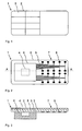
- Fig. 1 shows a plan view of the front side of an embodiment of an inventively designed chip module 1.
- a plan view of the back of the chip module 1 is in Fig. 2 shown.
- An associated section along the in Fig. 2 drawn section line AA shows Fig. 3 , These are only schematic representations that are not drawn to scale. This also applies to the other Fig.
- the chip module 1 is provided for installation in a chip card and has on its front side, which is directed to the installation of the chip module 1 to the outside, a contact pad 2.
- the contact field 2 can be designed in accordance with the ISO / IEC 7816 standard and consists of a series of contact surfaces 3, which can be contacted by means of a non-figuratively illustrated contacting unit of an external device.
- Fig. 2 shown back which is directed after installation in the smart card inward, has the chip module 1 in the region of the contact pad 2 an integrated circuit 4.
- the integrated circuit 4 is arranged on a carrier foil 5 and embedded in a potting body 6 for protection against damage.
- the contact field 2 is likewise arranged on the carrier foil 5, but on the front side of the chip module 1, and is produced for example by galvanic deposition.
- the contact surfaces 3 of the contact pad 2 are electrically connected to the integrated circuit 4.
- a connection pad 7 with a plurality of terminals 8 is formed on the carrier foil 5.
- connection pad 7 is arranged at a distance from the potting body 6 and thus also to the integrated circuit 4.
- the connection pad 7 is far removed from the potting body 6 such that a region of the carrier foil 5 which surrounds the potting body 6 and is adhesively bonded to the chip module 1 remains completely or largely recessed from the terminals 8 of the connection pad 7.
- the lateral distance of the connection pad 7 from the potting body 6 is preferably at least 2 mm.
- the connection pad 7 is also arranged laterally offset from the contact pad 2 and has approximately the same lateral dimensions as the contact pad 2, so that the lateral dimensions of the chip module 1 are approximately twice as large as the lateral dimensions of the contact pad 2.
- strip conductors 9 extend in the direction of the potting body 6.
- the strip conductors 9 are part of a circuit of the chip module 1 and can be electrically conductively connected to the integrated circuit 4, for example.
- connection panel 7 In a further education of in Fig. 1 to 3 illustrated embodiment of the chip module 1 are in the region of the connection panel 7 additionally electronic components, for example in SMD technology, applied.
- SMD stands for surface mounting devices and means that the electronic components are designed in miniaturized form and are soldered directly onto the conductor tracks 9 of the chip module 1.
- a switching device In the region of the connection field, a switching device, also not shown, may be formed. The switching device is preferably on the outside, ie on the in Fig.1 recognizable side, arranged. It may be, for example, a capacitive button or switch or an inductive circuit.
- Fig. 4 shows another top view of the back of the in the Fig. 1 to 3 illustrated embodiment of the chip module according to the invention 1.
- the conductor tracks 9 of the chip module 1 are omitted.
- conductor tracks 10 of the chip card are shown, which are arranged in the installed state of the chip module 1 in the manner shown relative to the connection pad 7 of the chip module 1. It is located in each case one end of the illustrated strip conductors 10 in the region of a respective connection 8, so that the strip conductors 10 can be electrically conductively connected to the connections 8.
- the interconnects 10 of the chip card are not formed on the carrier film 5 of the chip module 1, but part of the chip card.
- Fig. 5 shows a sectional view of an embodiment of the smart card according to the invention with the in the Fig. 1 to 4
- the cutting plane is chosen so that the chip module 1 in turn along the in Fig. 2 drawn line AA is cut.
- the chip card has a card body 11 with a two-step recess 12. In the recess 12, the chip module 1 is glued, wherein the bonding between the card body 11 and a surrounding the potting body 6 region of the carrier film 5 is formed.
- the lateral dimensions of the chip module 1 are significantly smaller than the lateral dimensions of the card body 11, which is shown only in part.
- the conductor tracks 10 of the chip card are accessible in the region of the recess 12 for the chip module 1.
- a conductive adhesive 13 in particular an ACF adhesive or an ACP adhesive, applied.
- ACF stands for Anisotropic Conductive Film, ACP for Anisotropic Conductive Paste.
- an adhesive 13 having an anisotropic conductivity When an adhesive 13 having an anisotropic conductivity is used, it is applied so that the conductivity is in-plane of the card body 11 is considerably less than perpendicular thereto. This makes it possible to apply the adhesive 13 in the area of the connection pad 7 of the chip module 1 over the entire surface, without thereby short-circuiting the terminals 8. However, it is also possible to use an adhesive 13 with an isotropic conductivity. In this case, care must be taken that the adhesive 13 is applied only at certain points in the area of the terminals 8 and that the adhesive points of various terminals 8 in the card body do not touch.
- the flexible bump method can be used, in which the terminals 8 of the chip module 1 lie directly against the conductor tracks 10 of the chip card and soldered to them or welded.
- connection pad 7 of the chip module 1 at a distance from the potting body 6, the mechanical stress of the connection pad 7, for example, at a bending stress of the card body 11, are kept relatively low, since a spatial separation of the stiffening acting potting 6 is present.
- connection pad 7 are accessible from outside the chip card. This can be achieved, for example, by arranging these connections 8 on the front side of the chip module 1.
- the externally accessible terminals 8, like the contact pad 2, can be contacted by a contacting unit of an external device. In this way, for example, a battery arranged in the card body 11 can be charged.
- connections 8 arranged on the front side of the chip module 1 are used as sensor sensors. These connections 8 may be connected to printed conductors 9 of the chip module 1 or to printed conductors 10 of the chip card and serve, for example, to switch functions of the chip card.
- connection pad 7 has additional components in addition to or as an alternative to the terminals 8. This is in Fig. 6 shown.
- Fig. 6 shows a plan view of the back of another embodiment of the chip module according to the invention 1.
- the conductor tracks 9 of the chip module 1 in the region of the connection pad 7 are arranged so that they form an antenna 14.
- An arrangement of the antenna 14 on the front and the back of the chip module 1 is conceivable.
- the antenna 14 may be electrically connected to two contact surfaces 3 of the contact pad 2, whereby an electrically conductive connection is formed to the integrated circuit.
- 7 electronic components in particular in SMD technology, can be applied in the region of the connection field.
- a switching device also not shown, may be formed.
- the switching device is preferably on the outside, ie on the in Fig.1 recognizable side, arranged. It may be, for example, a capacitive button or switch or an inductive circuit.
- the inventive concept can be applied to an arrangement of an antenna on a carrier.
- the antenna is then arranged at a lateral distance from the integrated circuit 4 on the carrier 5, without a connection pad is present.
- the other above-mentioned inventive aspects of an arrangement of a connection field are also applicable to the arrangement of an antenna.
- the chip module 1 for example, several terminal fields 7 may be provided, in particular two terminal panels 7 on opposite sides of the integrated circuit 4.
- the chip module 1 may be formed differently in terms of its basic structure.
- any standard method of chip module production can be used, for example the lead frame technique, in which the integrated circuit 4 is arranged on a punched-out contact pad 2, the flip chip technique, in which the integrated circuit 4 is arranged with its contact side on the carrier foil 5 etc.
- the chip card according to the invention can be designed for communication via a contacting contact or a contactless communication. Likewise, it is also possible that the chip card can communicate both via a contacting contact and contactless.
- a portable data carrier in the sense of the present invention is in particular a card-shaped data carrier, for example a chip card or a SIM module, a token, for example a USB token, or else a key fob.
Landscapes
- Engineering & Computer Science (AREA)
- Computer Hardware Design (AREA)
- Microelectronics & Electronic Packaging (AREA)
- Physics & Mathematics (AREA)
- General Physics & Mathematics (AREA)
- Theoretical Computer Science (AREA)
- Credit Cards Or The Like (AREA)
Claims (13)
- Module de puce destiné à support de données portable, comprenant un circuit intégré (4) qui est agencé sur un support (5), caractérisé en ce qu'une plage de connexion (7) à plusieurs bornes (8) pour la connexion d'au moins un composant électrique est réalisée sur le support (5) à un espacement latéral du circuit intégré (4), la plage de connexion (7) étant agencée à l'extérieur d'une zone de la feuille support (5) qui entoure le corps moulé, et la zone de la feuille support (5) qui entoure le corps moulé entourant le circuit intégré (4) ou un corps moulé (6) dans lequel le circuit intégré (4) est noyé.
- Module de puce selon une des revendications précédentes, caractérisé en ce qu'au moins quelques unes des bornes (8) sont connectées de manière électroconductrice avec le circuit intégré (4).
- Module de puce selon une des revendications précédentes, caractérisé en ce qu'au moins quelques unes des bornes (8) sont agencées sur la même face principale du support (5) sur laquelle est aussi agencé le circuit intégré (4).
- Module de puce selon une des revendications précédentes, caractérisé en ce que, dans la zone de la plage de connexion (7), au moins une élément capacitif et/ou au moins une élément inductif (14) est réalisé.
- Module de puce selon une des revendications précédentes, caractérisé en ce que, dans la zone de la plage de connexion (7), au moins un dispositif de commutation est réalisé.
- Module de puce selon une des revendications précédentes, caractérisé en ce que, dans la zone de la plage de connexion (7), au moins un composant électronique, de préférence en technique SMD, est agencé.
- Module de puce selon une des revendications précédentes, caractérisé en ce que le circuit intégré (4) est, pour une mise en contact externe, connecté de manière électroconductrice avec un champ de contact (2) standardisé.
- Module de puce selon la revendication 7, caractérisé en ce que la plage de connexion (7) est, pour la mise en contact externe, agencée de manière latéralement décalée par rapport au champ de contact (2).
- Support de données portable comprenant un corps de carte (11) qui comporte au moins un composant électronique, et un module de puce (1) selon la revendication 1, caractérisé en ce que la connexion électroconductrice est réalisée entre le module de puce (1) et le composant électronique du corps de carte (11) au moyen d'une plage de connexion (7) du module de puce (1) qui est réalisée sur le support (5) à un espacement latéral du circuit intégré (4) et comporte plusieurs bornes (8).
- Support de données portable selon la revendication 9, caractérisé en ce qu'au moins quelques bornes (8) de la plage de connexion (7) sont connectées, de manière électroconductrice au moyen d'une colle (13) électroconductrice présentant de préférence une conductivité anisotrope, avec des structures (10) du corps de carte (11) prévues à cet effet.
- Support de données portable selon une des revendications de 9 à 10, caractérisé en ce qu'au moins une borne (8) de la plage de connexion (7) est accessible à l'extérieur du corps de carte (11).
- Support de données portable selon une des revendications de 9 à 11, caractérisé en ce que les dimensions latérales du module de puce (1) sont inférieures aux dimensions latérales du corps de carte (11).
- Support de données portable selon une des revendications de 9 à 12, caractérisé en ce que le module de puce (1) est agencé dans un évidement (12) du corps de carte (11), lequel évidement est de préférence à deux niveaux et est ouvert vers le milieu extérieur.
Applications Claiming Priority (2)
| Application Number | Priority Date | Filing Date | Title |
|---|---|---|---|
| DE200410030749 DE102004030749A1 (de) | 2004-06-25 | 2004-06-25 | Chipmodul für einen tragbaren Datenträger |
| DE102004030749 | 2004-06-25 |
Publications (2)
| Publication Number | Publication Date |
|---|---|
| EP1610261A1 EP1610261A1 (fr) | 2005-12-28 |
| EP1610261B1 true EP1610261B1 (fr) | 2013-03-27 |
Family
ID=34937467
Family Applications (1)
| Application Number | Title | Priority Date | Filing Date |
|---|---|---|---|
| EP20050012874 Active EP1610261B1 (fr) | 2004-06-25 | 2005-06-15 | Module pour carte à puce |
Country Status (3)
| Country | Link |
|---|---|
| EP (1) | EP1610261B1 (fr) |
| DE (1) | DE102004030749A1 (fr) |
| ES (1) | ES2405263T3 (fr) |
Families Citing this family (2)
| Publication number | Priority date | Publication date | Assignee | Title |
|---|---|---|---|---|
| WO2008081224A1 (fr) * | 2006-12-28 | 2008-07-10 | Fci | Substrats plats pour cartes d'identification et procédés de fabrication de ceux-ci |
| DE102007054385A1 (de) * | 2007-11-14 | 2009-05-20 | Giesecke & Devrient Gmbh | Herstellen eines portablen Datenträgers |
Family Cites Families (7)
| Publication number | Priority date | Publication date | Assignee | Title |
|---|---|---|---|---|
| FR2634095A1 (fr) * | 1988-07-05 | 1990-01-12 | Bull Cp8 | Circuit imprime souple, notamment pour carte a microcircuits electroniques, et carte incorporant un tel circuit |
| DE19500925C2 (de) * | 1995-01-16 | 1999-04-08 | Orga Kartensysteme Gmbh | Verfahren zur Herstellung einer kontaktlosen Chipkarte |
| DE19721281C2 (de) * | 1997-05-21 | 1999-04-01 | Ods Landis & Gyr Gmbh & Co Kg | Chipmodul für eine Chipkarte |
| FR2780848A1 (fr) * | 1998-07-06 | 2000-01-07 | Solaic Sa | Antenne a bornes de connexion ajourees pour carte a circuit integre, et carte a circuit integre comprenant une telle antenne |
| DE19955538B4 (de) * | 1999-11-18 | 2014-06-05 | Morpho Cards Gmbh | Leiterbahnträgerschicht zur Einlaminierung in eine Chipkarte, Verfahren zur Herstellung einer Leiterbahnträgerschicht Spritzgusswerkzeug zur Durchführung des Verfahrens zur Herstellung einer Leiterbahnträgerschicht |
| US6376283B1 (en) * | 2000-04-19 | 2002-04-23 | Power Digital Card Co., Ltd. | Mono-chip multimediacard fabrication method |
| DE10120254A1 (de) | 2001-04-25 | 2002-11-07 | Infineon Technologies Ag | Chipkartenmodul |
-
2004
- 2004-06-25 DE DE200410030749 patent/DE102004030749A1/de not_active Withdrawn
-
2005
- 2005-06-15 EP EP20050012874 patent/EP1610261B1/fr active Active
- 2005-06-15 ES ES05012874T patent/ES2405263T3/es active Active
Also Published As
| Publication number | Publication date |
|---|---|
| EP1610261A1 (fr) | 2005-12-28 |
| DE102004030749A1 (de) | 2006-01-19 |
| ES2405263T3 (es) | 2013-05-30 |
Similar Documents
| Publication | Publication Date | Title |
|---|---|---|
| EP1429283B1 (fr) | Support de données portatif | |
| EP0886834B1 (fr) | Carte a puce et procede de fabrication d'une carte a puce | |
| EP1152368B1 (fr) | Carte à puce | |
| EP1553663B1 (fr) | Unité de contact pour supports de composants électroniques en forme de carte | |
| DE19940695B4 (de) | Elektronisches Mediagerät | |
| EP1816583B1 (fr) | Dispositif de contact pour une carte à puce | |
| EP0996932B1 (fr) | Support de donnees exploitable sans contact | |
| EP0891603B1 (fr) | Substrat non conducteur formant une bande ou un flanc, sur lequel sont formes une pluralite d'elements porteurs | |
| DE69000244T2 (de) | Chipkartensystem mit getrennter tragbarer elektronischer einheit. | |
| DE102020108927A1 (de) | Sensoreinrichtung, Verfahren zum Bilden einer Sensoreinrichtung, Trägerband, Chipkarte und Verfahren zum Bilden einer Chipkarte | |
| EP1610261B1 (fr) | Module pour carte à puce | |
| DE102013018518A1 (de) | IC-Modul für unterschiedliche Verbindungstechniken | |
| DE102005030794B4 (de) | Elektronisches Gerät mit einem Sicherheitsmodul | |
| EP2700055B1 (fr) | Transducteur d'identification pour un système d'accès à un véhicule automobile avec un sous-ensemble nfc amovible | |
| DE10108080C1 (de) | Kontaktlos arbeitender Datenträger mit einer kapazitiv an das Modul gekoppelten Antennenspule | |
| DE102007022615A1 (de) | Kontaktloses Übertragungssystem und Verfahren zum Herstellen desselben | |
| DE102010028868A1 (de) | Halbleitersubstratbasierte Anordnung für eine RFID-Einrichtung, RFID-Einrichtung und Verfahren zur Herstellung einer solchen halbleitersubstratbasierten Anordnung | |
| EP1695454B1 (fr) | Appareil electronique pourvu d'un module de securite | |
| EP1684216A1 (fr) | Support de données portatif | |
| EP1352362B1 (fr) | Ensemble support de donnees comprenant un dispositif d'affichage | |
| EP1668571B1 (fr) | Support de donnees portable | |
| EP1472650B1 (fr) | Pile a membrane pourvue d'un composant integre et connue pour etre utilisee dans une carte a puce | |
| DE102005002728A1 (de) | Tragbarer Datenträger | |
| DE19612718B4 (de) | Chipkarte mit Batterie sowie Verfahren zur Montage einer Chipmodul/Batterie-Einheit | |
| DE102005002733B4 (de) | Tragbarer Datenträger |
Legal Events
| Date | Code | Title | Description |
|---|---|---|---|
| PUAI | Public reference made under article 153(3) epc to a published international application that has entered the european phase |
Free format text: ORIGINAL CODE: 0009012 |
|
| AK | Designated contracting states |
Kind code of ref document: A1 Designated state(s): AT BE BG CH CY CZ DE DK EE ES FI FR GB GR HU IE IS IT LI LT LU MC NL PL PT RO SE SI SK TR |
|
| AX | Request for extension of the european patent |
Extension state: AL BA HR LV MK YU |
|
| 17P | Request for examination filed |
Effective date: 20060628 |
|
| AKX | Designation fees paid |
Designated state(s): AT BE BG CH CY CZ DE DK EE ES FI FR GB GR HU IE IS IT LI LT LU MC NL PL PT RO SE SI SK TR |
|
| 17Q | First examination report despatched |
Effective date: 20060831 |
|
| GRAP | Despatch of communication of intention to grant a patent |
Free format text: ORIGINAL CODE: EPIDOSNIGR1 |
|
| GRAS | Grant fee paid |
Free format text: ORIGINAL CODE: EPIDOSNIGR3 |
|
| GRAA | (expected) grant |
Free format text: ORIGINAL CODE: 0009210 |
|
| AK | Designated contracting states |
Kind code of ref document: B1 Designated state(s): AT BE BG CH CY CZ DE DK EE ES FI FR GB GR HU IE IS IT LI LT LU MC NL PL PT RO SE SI SK TR |
|
| REG | Reference to a national code |
Ref country code: GB Ref legal event code: FG4D Free format text: NOT ENGLISH Ref country code: DE Ref legal event code: R081 Ref document number: 502005013578 Country of ref document: DE Owner name: GIESECKE+DEVRIENT MOBILE SECURITY GMBH, DE Free format text: FORMER OWNER: GIESECKE & DEVRIENT GMBH, 81677 MUENCHEN, DE |
|
| REG | Reference to a national code |
Ref country code: CH Ref legal event code: EP |
|
| REG | Reference to a national code |
Ref country code: AT Ref legal event code: REF Ref document number: 603810 Country of ref document: AT Kind code of ref document: T Effective date: 20130415 |
|
| REG | Reference to a national code |
Ref country code: IE Ref legal event code: FG4D Free format text: LANGUAGE OF EP DOCUMENT: GERMAN |
|
| REG | Reference to a national code |
Ref country code: DE Ref legal event code: R096 Ref document number: 502005013578 Country of ref document: DE Effective date: 20130523 |
|
| REG | Reference to a national code |
Ref country code: ES Ref legal event code: FG2A Ref document number: 2405263 Country of ref document: ES Kind code of ref document: T3 Effective date: 20130530 |
|
| PG25 | Lapsed in a contracting state [announced via postgrant information from national office to epo] |
Ref country code: SE Free format text: LAPSE BECAUSE OF FAILURE TO SUBMIT A TRANSLATION OF THE DESCRIPTION OR TO PAY THE FEE WITHIN THE PRESCRIBED TIME-LIMIT Effective date: 20130327 Ref country code: BG Free format text: LAPSE BECAUSE OF FAILURE TO SUBMIT A TRANSLATION OF THE DESCRIPTION OR TO PAY THE FEE WITHIN THE PRESCRIBED TIME-LIMIT Effective date: 20130627 Ref country code: LT Free format text: LAPSE BECAUSE OF FAILURE TO SUBMIT A TRANSLATION OF THE DESCRIPTION OR TO PAY THE FEE WITHIN THE PRESCRIBED TIME-LIMIT Effective date: 20130327 |
|
| REG | Reference to a national code |
Ref country code: SK Ref legal event code: T3 Ref document number: E 14142 Country of ref document: SK |
|
| REG | Reference to a national code |
Ref country code: LT Ref legal event code: MG4D |
|
| PG25 | Lapsed in a contracting state [announced via postgrant information from national office to epo] |
Ref country code: FI Free format text: LAPSE BECAUSE OF FAILURE TO SUBMIT A TRANSLATION OF THE DESCRIPTION OR TO PAY THE FEE WITHIN THE PRESCRIBED TIME-LIMIT Effective date: 20130327 Ref country code: GR Free format text: LAPSE BECAUSE OF FAILURE TO SUBMIT A TRANSLATION OF THE DESCRIPTION OR TO PAY THE FEE WITHIN THE PRESCRIBED TIME-LIMIT Effective date: 20130628 Ref country code: SI Free format text: LAPSE BECAUSE OF FAILURE TO SUBMIT A TRANSLATION OF THE DESCRIPTION OR TO PAY THE FEE WITHIN THE PRESCRIBED TIME-LIMIT Effective date: 20130327 |
|
| REG | Reference to a national code |
Ref country code: NL Ref legal event code: VDEP Effective date: 20130327 |
|
| PG25 | Lapsed in a contracting state [announced via postgrant information from national office to epo] |
Ref country code: NL Free format text: LAPSE BECAUSE OF FAILURE TO SUBMIT A TRANSLATION OF THE DESCRIPTION OR TO PAY THE FEE WITHIN THE PRESCRIBED TIME-LIMIT Effective date: 20130327 Ref country code: RO Free format text: LAPSE BECAUSE OF FAILURE TO SUBMIT A TRANSLATION OF THE DESCRIPTION OR TO PAY THE FEE WITHIN THE PRESCRIBED TIME-LIMIT Effective date: 20130327 Ref country code: PT Free format text: LAPSE BECAUSE OF FAILURE TO SUBMIT A TRANSLATION OF THE DESCRIPTION OR TO PAY THE FEE WITHIN THE PRESCRIBED TIME-LIMIT Effective date: 20130729 Ref country code: IS Free format text: LAPSE BECAUSE OF FAILURE TO SUBMIT A TRANSLATION OF THE DESCRIPTION OR TO PAY THE FEE WITHIN THE PRESCRIBED TIME-LIMIT Effective date: 20130727 Ref country code: CZ Free format text: LAPSE BECAUSE OF FAILURE TO SUBMIT A TRANSLATION OF THE DESCRIPTION OR TO PAY THE FEE WITHIN THE PRESCRIBED TIME-LIMIT Effective date: 20130327 Ref country code: EE Free format text: LAPSE BECAUSE OF FAILURE TO SUBMIT A TRANSLATION OF THE DESCRIPTION OR TO PAY THE FEE WITHIN THE PRESCRIBED TIME-LIMIT Effective date: 20130327 |
|
| PG25 | Lapsed in a contracting state [announced via postgrant information from national office to epo] |
Ref country code: CY Free format text: LAPSE BECAUSE OF FAILURE TO SUBMIT A TRANSLATION OF THE DESCRIPTION OR TO PAY THE FEE WITHIN THE PRESCRIBED TIME-LIMIT Effective date: 20130327 Ref country code: PL Free format text: LAPSE BECAUSE OF FAILURE TO SUBMIT A TRANSLATION OF THE DESCRIPTION OR TO PAY THE FEE WITHIN THE PRESCRIBED TIME-LIMIT Effective date: 20130327 |
|
| BERE | Be: lapsed |
Owner name: GIESECKE & DEVRIENT G.M.B.H. Effective date: 20130630 |
|
| PG25 | Lapsed in a contracting state [announced via postgrant information from national office to epo] |
Ref country code: MC Free format text: LAPSE BECAUSE OF FAILURE TO SUBMIT A TRANSLATION OF THE DESCRIPTION OR TO PAY THE FEE WITHIN THE PRESCRIBED TIME-LIMIT Effective date: 20130327 Ref country code: DK Free format text: LAPSE BECAUSE OF FAILURE TO SUBMIT A TRANSLATION OF THE DESCRIPTION OR TO PAY THE FEE WITHIN THE PRESCRIBED TIME-LIMIT Effective date: 20130327 |
|
| PLBE | No opposition filed within time limit |
Free format text: ORIGINAL CODE: 0009261 |
|
| REG | Reference to a national code |
Ref country code: CH Ref legal event code: PL |
|
| STAA | Information on the status of an ep patent application or granted ep patent |
Free format text: STATUS: NO OPPOSITION FILED WITHIN TIME LIMIT |
|
| PG25 | Lapsed in a contracting state [announced via postgrant information from national office to epo] |
Ref country code: IT Free format text: LAPSE BECAUSE OF FAILURE TO SUBMIT A TRANSLATION OF THE DESCRIPTION OR TO PAY THE FEE WITHIN THE PRESCRIBED TIME-LIMIT Effective date: 20130327 |
|
| 26N | No opposition filed |
Effective date: 20140103 |
|
| REG | Reference to a national code |
Ref country code: IE Ref legal event code: MM4A |
|
| PG25 | Lapsed in a contracting state [announced via postgrant information from national office to epo] |
Ref country code: BE Free format text: LAPSE BECAUSE OF NON-PAYMENT OF DUE FEES Effective date: 20130630 |
|
| REG | Reference to a national code |
Ref country code: DE Ref legal event code: R097 Ref document number: 502005013578 Country of ref document: DE Effective date: 20140103 |
|
| PG25 | Lapsed in a contracting state [announced via postgrant information from national office to epo] |
Ref country code: LI Free format text: LAPSE BECAUSE OF NON-PAYMENT OF DUE FEES Effective date: 20130630 Ref country code: IE Free format text: LAPSE BECAUSE OF NON-PAYMENT OF DUE FEES Effective date: 20130615 Ref country code: CH Free format text: LAPSE BECAUSE OF NON-PAYMENT OF DUE FEES Effective date: 20130630 |
|
| REG | Reference to a national code |
Ref country code: AT Ref legal event code: MM01 Ref document number: 603810 Country of ref document: AT Kind code of ref document: T Effective date: 20130615 |
|
| PG25 | Lapsed in a contracting state [announced via postgrant information from national office to epo] |
Ref country code: AT Free format text: LAPSE BECAUSE OF NON-PAYMENT OF DUE FEES Effective date: 20130615 |
|
| REG | Reference to a national code |
Ref country code: FR Ref legal event code: PLFP Year of fee payment: 11 |
|
| PG25 | Lapsed in a contracting state [announced via postgrant information from national office to epo] |
Ref country code: TR Free format text: LAPSE BECAUSE OF FAILURE TO SUBMIT A TRANSLATION OF THE DESCRIPTION OR TO PAY THE FEE WITHIN THE PRESCRIBED TIME-LIMIT Effective date: 20130327 |
|
| PG25 | Lapsed in a contracting state [announced via postgrant information from national office to epo] |
Ref country code: HU Free format text: LAPSE BECAUSE OF FAILURE TO SUBMIT A TRANSLATION OF THE DESCRIPTION OR TO PAY THE FEE WITHIN THE PRESCRIBED TIME-LIMIT; INVALID AB INITIO Effective date: 20050615 Ref country code: LU Free format text: LAPSE BECAUSE OF NON-PAYMENT OF DUE FEES Effective date: 20130615 |
|
| REG | Reference to a national code |
Ref country code: FR Ref legal event code: PLFP Year of fee payment: 12 |
|
| REG | Reference to a national code |
Ref country code: FR Ref legal event code: PLFP Year of fee payment: 13 |
|
| REG | Reference to a national code |
Ref country code: DE Ref legal event code: R081 Ref document number: 502005013578 Country of ref document: DE Owner name: GIESECKE+DEVRIENT MOBILE SECURITY GMBH, DE Free format text: FORMER OWNER: GIESECKE & DEVRIENT GMBH, 81677 MUENCHEN, DE |
|
| PGFP | Annual fee paid to national office [announced via postgrant information from national office to epo] |
Ref country code: CZ Payment date: 20170411 Year of fee payment: 13 |
|
| REG | Reference to a national code |
Ref country code: GB Ref legal event code: 732E Free format text: REGISTERED BETWEEN 20180118 AND 20180124 |
|
| REG | Reference to a national code |
Ref country code: SK Ref legal event code: PC4A Ref document number: E 14142 Country of ref document: SK Owner name: GIESECKE+DEVRIENT MOBILE SECURITY GMBH, MUENCH, DE Free format text: FORMER OWNER: GIESECKE & DEVRIENT GMBH, MUENCHEN, DE Effective date: 20171120 |
|
| REG | Reference to a national code |
Ref country code: FR Ref legal event code: PLFP Year of fee payment: 14 |
|
| REG | Reference to a national code |
Ref country code: FR Ref legal event code: TP Owner name: GIESECKE+DEVRIENT MOBILE SECURITY GMBH, DE Effective date: 20180619 |
|
| REG | Reference to a national code |
Ref country code: SK Ref legal event code: MM4A Ref document number: E 14142 Country of ref document: SK Effective date: 20180615 |
|
| PG25 | Lapsed in a contracting state [announced via postgrant information from national office to epo] |
Ref country code: SK Free format text: LAPSE BECAUSE OF NON-PAYMENT OF DUE FEES Effective date: 20180615 |
|
| P01 | Opt-out of the competence of the unified patent court (upc) registered |
Effective date: 20230520 |
|
| REG | Reference to a national code |
Ref country code: DE Ref legal event code: R081 Ref document number: 502005013578 Country of ref document: DE Owner name: GIESECKE+DEVRIENT EPAYMENTS GMBH, DE Free format text: FORMER OWNER: GIESECKE+DEVRIENT MOBILE SECURITY GMBH, 81677 MUENCHEN, DE |
|
| PGFP | Annual fee paid to national office [announced via postgrant information from national office to epo] |
Ref country code: FR Payment date: 20230620 Year of fee payment: 19 Ref country code: DE Payment date: 20230630 Year of fee payment: 19 |
|
| PGFP | Annual fee paid to national office [announced via postgrant information from national office to epo] |
Ref country code: GB Payment date: 20230622 Year of fee payment: 19 Ref country code: ES Payment date: 20230719 Year of fee payment: 19 |