EP1608054B1 - Controlling a power converter - Google Patents
Controlling a power converter Download PDFInfo
- Publication number
- EP1608054B1 EP1608054B1 EP05105040.9A EP05105040A EP1608054B1 EP 1608054 B1 EP1608054 B1 EP 1608054B1 EP 05105040 A EP05105040 A EP 05105040A EP 1608054 B1 EP1608054 B1 EP 1608054B1
- Authority
- EP
- European Patent Office
- Prior art keywords
- converter
- capacitive element
- voltage
- power
- audio amplifier
- Prior art date
- Legal status (The legal status is an assumption and is not a legal conclusion. Google has not performed a legal analysis and makes no representation as to the accuracy of the status listed.)
- Expired - Lifetime
Links
Images


Classifications
-
- H—ELECTRICITY
- H02—GENERATION; CONVERSION OR DISTRIBUTION OF ELECTRIC POWER
- H02M—APPARATUS FOR CONVERSION BETWEEN AC AND AC, BETWEEN AC AND DC, OR BETWEEN DC AND DC, AND FOR USE WITH MAINS OR SIMILAR POWER SUPPLY SYSTEMS; CONVERSION OF DC OR AC INPUT POWER INTO SURGE OUTPUT POWER; CONTROL OR REGULATION THEREOF
- H02M3/00—Conversion of DC power input into DC power output
- H02M3/02—Conversion of DC power input into DC power output without intermediate conversion into AC
- H02M3/04—Conversion of DC power input into DC power output without intermediate conversion into AC by static converters
- H02M3/10—Conversion of DC power input into DC power output without intermediate conversion into AC by static converters using discharge tubes with control electrode or semiconductor devices with control electrode
- H02M3/145—Conversion of DC power input into DC power output without intermediate conversion into AC by static converters using discharge tubes with control electrode or semiconductor devices with control electrode using devices of a triode or transistor type requiring continuous application of a control signal
- H02M3/155—Conversion of DC power input into DC power output without intermediate conversion into AC by static converters using discharge tubes with control electrode or semiconductor devices with control electrode using devices of a triode or transistor type requiring continuous application of a control signal using semiconductor devices only
- H02M3/156—Conversion of DC power input into DC power output without intermediate conversion into AC by static converters using discharge tubes with control electrode or semiconductor devices with control electrode using devices of a triode or transistor type requiring continuous application of a control signal using semiconductor devices only with automatic control of output voltage or current, e.g. switching regulators
-
- H—ELECTRICITY
- H02—GENERATION; CONVERSION OR DISTRIBUTION OF ELECTRIC POWER
- H02J—CIRCUIT ARRANGEMENTS OR SYSTEMS FOR SUPPLYING OR DISTRIBUTING ELECTRIC POWER; SYSTEMS FOR STORING ELECTRIC ENERGY
- H02J7/00—Circuit arrangements for charging or depolarising batteries or for supplying loads from batteries
- H02J7/34—Parallel operation in networks using both storage and other DC sources, e.g. providing buffering
- H02J7/345—Parallel operation in networks using both storage and other DC sources, e.g. providing buffering using capacitors as storage or buffering devices
-
- H—ELECTRICITY
- H02—GENERATION; CONVERSION OR DISTRIBUTION OF ELECTRIC POWER
- H02M—APPARATUS FOR CONVERSION BETWEEN AC AND AC, BETWEEN AC AND DC, OR BETWEEN DC AND DC, AND FOR USE WITH MAINS OR SIMILAR POWER SUPPLY SYSTEMS; CONVERSION OF DC OR AC INPUT POWER INTO SURGE OUTPUT POWER; CONTROL OR REGULATION THEREOF
- H02M1/00—Details of apparatus for conversion
- H02M1/0003—Details of control, feedback or regulation circuits
- H02M1/0016—Control circuits providing compensation of output voltage deviations using feedforward of disturbance parameters
- H02M1/0019—Control circuits providing compensation of output voltage deviations using feedforward of disturbance parameters the disturbance parameters being load current fluctuations
Definitions
- This description relates to controlling a power converter.
- Power converters are used to supply power to a load. Some power converters are DC-DC converters supplying direct current (DC) power from a DC source such as a battery. Other power converters are AC-DC converters supplying DC power from an alternating current (AC) source such as a wall outlet. In some cases a capacitor in parallel with the power converter (e.g., a "super capacitor”) is used as a back-up source.
- DC direct current
- AC alternating current
- a capacitor in parallel with the power converter e.g., a "super capacitor” is used as a back-up source.
- EP-A-0657985 describes a power supply system for delivering power to a load including a capacitive element, a converter in parallel with the capacitive element to operate so that a reduction of the input impedance of the load causes an increase in a time constant for supplying additional power to the load by the capacitive element.
- a method comprises, in response to a change in a circuit parameter of a converter delivering power to an audio amplifier, operating the converter in a mode in which additional power is supplied to the audio amplifier by a capacitive element that is coupled in parallel with the converter, wherein the audio amplifier includes either a compressor having a threshold that is a function of the voltage supplied to the audio amplifier or a variable gain circuit such that the gain of the audio amplifier is a function of the voltage supplied to the audio amplifier.
- the invention also includes an apparatus comprising a capacitive element; an audio amplifier; and a power converter, the capacitive element coupled in parallel to an output of the converter, such that in response to a change in a circuit parameter of the converter, the apparatus will operate in a mode in which additional power is supplied to the audio amplifier by the capacitive element, wherein the audio amplifier includes either a compressor having a threshold that is a function of the voltage supplied to the audio amplifier or a variable gain circuit such that the gain of the audio amplifier is a function of the voltage supplied to the audio amplifier.
- the gain of the audio amplifier may be variable and may be a function of a voltage supplied to the audio amplifier by the converter.
- the audio amplifier is capable of operating without clipping over a range of values of the voltage.
- the gain of the audio amplifier is preferably proportional to the voltage over at least a portion of a range of possible values of the voltage.
- the circuit parameter may be one of output current, input current, input power, or temperature of a component of the converter.
- the converter may act as a voltage source in a first mode and as a current source in a second mode.
- the amplifier may include a compressor that has a threshold that is a function of a parameter indicative of an amplified signal level.
- the capacitive element is preferably a super-capacitive element, and the converter characteristics are chosen such that the voltage of the super-capacitive element discharges by at least about 20%, preferably by at least about 50%.
- the capacitive element is coupled to output power terminals of the converter.
- the audio amplifier is preferably in parallel with the capacitive element and the converter is in parallel with the capacitive element and the amplifier.
- the audio amplifier includes a signal compressor that has a threshold that is a function of a voltage supplied to the audio amplifier by the converter.
- the invention features an apparatus that includes a capacitive element, an amplifier in parallel with the capacitive element, and a converter in parallel with the capacitive element and the amplifier to, in response to a change in a circuit parameter of the converter, operate in a mode in which power is supplied to the amplifier by the capacitive element, wherein the gain of the amplifier is a function of a parameter indicative of an amplified signal level.
- the invention features an apparatus for delivering power to a load.
- the apparatus includes a capacitive element, and a converter in parallel with the capacitive element to operate so that the current-voltage characteristic of the converter has a knee at a predefined current value, such that a reduction of the input impedance of the load causes an increase in a time constant for supplying additional power to the load by the capacitive element.
- Controlling a power converter to cause power to be supplied to a load by a capacitor enables high peak power to be supplied to the load.
- controlling current-voltage characteristics of the power converter by sensing converter input current from the battery increases battery life and reliability.
- Controlling current-voltage characteristics of a power converter by sensing converter output current prevents overload of the converter output components.
- FIG. 1 shows a circuit that includes a power converter 100 in parallel with a capacitive element 102 (e.g., circuitry having an impedance with negative reactance).
- the power converter 100 and capacitive element 102 are coupled to a load 104 that demands an amount of power P L based on the input resistance R L of the load 104.
- the input resistance R L ( t ) varies as a function of time t .
- variable loads e.g., an audio power amplifier or a motor
- a power converter 100 with a controlled current-voltage characteristic is able to supply the average power demanded by the load, while causing a brief demand for a high peak power to be supplied from energy stored in the capacitive element 102.
- the power converter 100 can maintain a relatively low amount of power drawn from a power source such as a battery or AC mains.
- a DC-DC power converter 200A in parallel with a capacitive element 202A can be used to supply power to an audio amplifier 204 from a battery 206 ( FIG. 2A ), and an AC-DC power converter 200B in parallel with a capacitive element 202B can be used to supply power to the audio amplifier 204 from an AC mains 208 ( FIG. 2B ).
- the varying nature of the power demand from the audio amplifier 204 is determined, for example, by a music signal 210 that is amplified to drive a speaker 212.
- a power converter and capacitive element can be used to supply power to other types of devices or combinations of devices where power demand may vary (e.g., a charging cradle for a cell phone, where the cradle also acts as a powered loudspeaker and many other examples).
- power demand may vary (e.g., a charging cradle for a cell phone, where the cradle also acts as a powered loudspeaker and many other examples).
- the capacitive element 202A can be implemented using a "super capacitor” or “ultra capacitor” (e.g., using aerogel technology) to obtain a capacitance in the range of approximately 1-30 Farads (F) and a maximum voltage of approximately 2.5 V.
- the capacitive element 202B includes two 10 F/2.5 V capacitors in series, each capacitor having a 5.1 k ⁇ shunt resistor (e.g., to provide even steady-state charge storage among the capacitors).
- the resulting capacitance of the capacitive element 202B is 5 F, and the maximum voltage of the capacitive element 202B is 5 V.
- the capacitive element can include three or more capacitors connected in series. Any of a variety of implementations of a capacitive element including 202A, 202B or others may be used in any of a variety of power converter configurations including a DC-DC power converter, an AC-DC power converter or others.
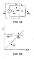
- FIG. 3A shows a circuit with a voltage source 300 and a load resistor 310.
- the voltage source 300 e.g., a Li-Ion or NiMHd battery
- the voltage source 300 is modeled by an ideal voltage source 302 (of constant voltage V 0 ) in series with a resistor 304 representing the output resistance of the voltage source 300.
- the current-voltage characteristic 306 for this voltage source 300 is shown in FIG. 3B , along with the "load line" for the load 310 (i.e., the current-voltage characteristic of the load resistor 310).
- the small output resistance R V represented by the resistor 304 causes a sag 308 in the output voltage V V of the voltage source 300 as a function of output current I V .
- the size of the sag 308 increases as the load resistance R L (i.e., the slope of the load line) decreases.
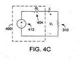
- FIG. 4A shows a circuit with a current source 400 and a load resistor 310.
- the current source 400 is modeled by an ideal current source 402 (of constant current I 0 ) in parallel with a resistor 404 representing the output resistance of the current source 400.
- the current-voltage characteristic 406 for this current source 400 is shown in FIG. 4B , along with the load line for the load resistor 310.
- the large output resistance R I represented by the resistor 404 causes a sag 408 in the output current I I of the current source 400 as a function of output voltage V I .
- the size of the sag 408 increases as the load resistance R L increases.
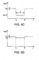
- FIG. 5A shows an example of a power converter 500 in parallel with a capacitor 502.
- the power converter and the capacitor cooperatively supply power to a variable load 504.
- the power converter 500 has a current-voltage characteristic 506 as shown in FIG. 5B .
- the power converter 500 has the characteristics of the voltage source 300 (e.g., has a low effective output resistance R V ) for output current I S values from 0 to I A and has the characteristics of the current source 400 (e.g., has a high effective output resistance R I ) for output current I S above I A , limiting the current that can be supplied from the power converter 500.
- the nominal load line 510 intersects the current-voltage characteristic 506 at a current I 1 and a voltage V 1 .
- the peak load line 512 intersects the current-voltage characteristic 506 at a current I 2 that is larger than I 1 , and a voltage V 2 that is slightly lower than V 1 .
- These intersections of the load lines with the current-voltage characteristic 506 give the asymptotic "DC solutions" for current and voltage after transients due to the capacitor 502 decay.
- the capacitor 502 provides continuity in the change of the capacitor voltage (equal to V S ( t )) over time.
- FIG. 5D shows the voltage V S ( t ) across the power converter 500, the capacitor 502, and the variable load 504 as a function of time.
- the voltage V S ( t ) rises exponentially back to V 1 with the same time constant ⁇ A .
- the change in voltage V S ( t ) only lasts for a small fraction of the time interval T, causing d V S t d t and thus the power I C ( t ) V S ( t ) supplied by the capacitor 502 to be limited.
- the current limit can be lowered to correspond to the expected peak demand of the variable load 504 so that the power converter 500 provides a dual-mode capability, as described in the next example ( FIGS. 6A- 6D ).
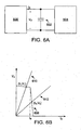
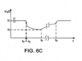
- FIG. 6A shows an example of a power converter 500' in parallel with a capacitor 502 cooperatively supplying power to a variable load 504.
- the power converter 500' has a current-voltage characteristic 606 as shown in FIG. 6B .
- the power converter 500' has the characteristics of the voltage source 300 (e.g., has a low effective output resistance) for output current I S values from 0 to I B and has the characteristics of the current source 400 (e.g., has a high effective output resistance) for output current I S above I B .
- variable load 504 temporarily demands more power by dropping an input resistance R L ( t ) from a value of R 0 (corresponding to a "nominal" load line 610) to a value of R 0 /3 (corresponding to load line 612) over a time period T , after which the resistance returns to the value R 0 , as shown in the plot of FIG. 5C .
- the nominal load line 610 intersects the current-voltage characteristic 606 at a current I 1 and a voltage V 1 , as in the previous example ( FIG. 5B ). However, in this example ( FIG. 6B ), the peak load line 612 intersects the current-voltage characteristic 606 at a current I 3 that is larger than I 1 but less than I 2 and a voltage V 3 that is substantially lower than V 1 and V 2 . These intersections of the load lines with the current-voltage characteristic 606 also give the asymptotic DC solutions for current and voltage.
- FIG. 6C shows the voltage V S ( t ) across the power converter 500', the capacitor 502, and the variable load 504 as a function of time.
- V 3 is substantially lower than V 1 , the capacitor 502 is able to discharge deeply (e.g., by about 50% in this example).
- the power converter 500' switches back to the voltage source mode.
- the change in voltage V S ( t ) lasts over the entire time interval T , causing V S t d t and thus the power I C ( t ) V S ( t ) supplied by the capacitor 502 to be large enough to supply most of the additional power in a brief demand for more power by a variable load.
- a variable load such as an audio power amplifier may exhibit a continuous change in input resistance R L ( t ) with a more complex time dependency having changes that follow time scales present in a music signal (e.g., on the order of milliseconds or as high as tens of seconds) that represent a brief demand for a high peak power.
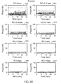
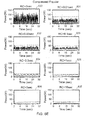
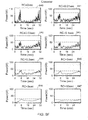
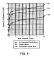
- Examples of power consumption dynamics for different types of music are shown in FIGS. 6D - 6F .
- the plots shown in FIGS. 6D - 6F are based on a simulated typical audio system, incorporating power converter control as described herein, playing exemplary music passages of different music types.
- the vertical axis gives instantaneous residual power drawn from the power source in Watts
- the horizontal axis gives time in seconds.
- Each of the plots 620 - 627 corresponds to a different time constant labeled as "RC.”
- the peak residual power for each plot is shown as a dotted line.
- peak residual power is progressively reduced from about 40 W (plot 621) to about 7 W (plot 627) when RC is increased from 0.01 seconds (plot 621) to 10 seconds (plot 627).
- FIG. 6E shows similar plots 630 - 637 for an exemplary passage of compressed popular music.
- peak residual power is reduced from about 70 W (plot 631) to about 20 W (plot 637) when RC is increased from 0.01 seconds (plot 631) to 10 seconds (plot 637).
- FIG. 6F shows similar plots 640 - 647 for an exemplary passage of classical music.
- peak residual power is reduced from about 67 W (plot 641) to about 20 W (plot 647) when RC is increased from 0.01 seconds (plot 641) to 10 seconds (plot 647).
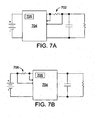
- the DC-DC power converter 200A ( FIG. 2A ) can use any of a variety of parameters to implement the dual-mode capabilities described above.
- the circuit in FIG. 7A includes a resistor 702 for sensing the output current of a switching power supply 704. The voltage across the resistor 702 is fed back to the switching power supply 704 and used to control the output voltage according to a desired current-voltage characteristic.
- the circuit in FIG. 7B includes a resistor 706 for sensing the input current of the switching power supply 704 for achieving a desired current-voltage characteristic.
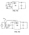
- the circuit in FIG. 7C includes circuitry 708 for sensing the input power of the switching power supply 704.
- the circuitry 708 generates a voltage 710 that is the product of the input voltage and a voltage proportional to the input current, and is therefore proportional to the input power.
- a voltage 710 that is the product of the input voltage and a voltage proportional to the input current, and is therefore proportional to the input power.
- the power supply 704 When the input power is below a threshold power level the power supply 704 operates according to a current-voltage characteristic of a first mode, and when the input power is above the threshold power level the power supply 704 operates according to a current-voltage characteristic of a second mode. Other parameters can be used to control the current-voltage characteristic of the switching power supply 704.
- the power supply 704 includes a control module 705 to switch modes based on the sensed parameter. One possible implementation of such a control module is described in more detail below (e.g., control module 814 in FIG. 8 ).
- the switching power supply 704 can use any of a variety of low-loss conversion techniques (e.g., a boost converter, a buck converter, a flyback converter, or a single-ended primary inductance converter).
- low-loss conversion techniques e.g., a boost converter, a buck converter, a flyback converter, or a single-ended primary inductance converter.
- an AC-DC converter 712 includes circuitry 714 for sensing the temperature of the AC transformer core 716.
- the AC-DC converter 712 switches between different current-voltage characteristics (i.e., different modes) based on comparing the sensed temperature to a threshold temperature.
- temperature may optionally be used in conjunction with other control parameters (e.g., output current, input power, input current, etc.).
- temperature modifies the current-voltage characteristic (e.g., by making I B a function of temperature).
- Other parameters can be used to control the current-voltage characteristic of the switching converter 712.
- the converter 712 also includes a control module 705 to switch modes based on the sensed parameter.
- the trigger condition that causes the control module 705 to switch modes is programmable (e.g., by programming the trigger condition into a microprocessor).
- the converter 712 senses various circuit parameters (e.g., input power, output current, temperature, etc.) and the circuit parameter that is used by the control module 705 to switch modes is programmable.
- the value of a circuit parameter that triggers a change in modes can be programmable.
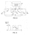
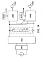
- FIG. 8 shows a Boost type power converter circuit 800 implementing the sensing technique of FIG. 7A .
- the input of the circuit 800 is connected to a battery 802 with voltage V B and the output of the circuit 800 is coupled to a capacitor 804 in parallel with a variable load 806.
- the circuit 800 includes an inductor 808, a diode 810, and a switch 812 that is controlled by a control module 814 based on the output current I out ( t ) in a sensing resistor 816.
- the circuit 800 also includes a capacitor 818 with a relatively small capacitance to filter out much of the switching frequency, and reduce ripple on the output voltage.
- the control module 814 includes a microprocessor for controlling the switch operation as a function of sensed output current.
- the resistance R S of the sensing resistor 816 is small compared to the load resistance R L ( t ).
- the output voltage V out ( t ) is higher than the constant input voltage V B .
- a control module using other control parameters can be implemented in a similar way.
- the duty cycle of a Boost type or other type of switching power converter can be a function of input power when the input power crosses a threshold value.
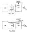
- FIGS. 10A and 10B show exemplary current-voltage characteristics for a power converter that can be used to cause a capacitive element to discharge deeply to supply more power to a variable load.
- the characteristic 1002 has a first mode 1004 characterized by a shallow slope of the voltage versus current plot, and a second mode 1006 in which the current I S is limited to a maximum current I th for voltages V S below a transition voltage V T .
- V T transition voltage
- the first mode 1004 may be achieved by setting R out in Equation (4) to small value for I S values less than I th and the second mode 1006 may be achieved by setting R out in Equation (4) to a large value for I S values equal to or greater than I th .
- the characteristic 1008 has a first mode 1010 characterized by a shallow slope of the voltage versus current plot, and a second mode 1012 characterized by a steep slope of the voltage versus current plot. Between the first and second modes, the characteristic 1008 has a "transition zone" 1014 that has a "knee" 1016 in the voltage versus current plot.
- the first mode 1010 may be achieved by setting R out in Equation (4) to a small value for I S values less than I th .
- the transition zone 1014 and second mode 1012 may be achieved by setting R out in Equation (4) to an increasing value as a function of I S for I S values equal to or greater than I th .
- the value of D in Equation (4) can be controlled using a programmable device (e.g., a microprocessor).
- the value of R out in Equation (4) can be controlled (as a function of I S ) in software, for example, using a look-up table or a polynomial curve fit.
- the transition between modes and the slope of the voltage versus current plot can be selected to ensure a minimum operating voltage (e.g., for an audio amplifier) is maintained for a given peak demand (e.g., minimum load resistance).
- the transition between modes can optionally be tunable.
- an audio amplifier 1100 includes a compressor 1102 with a threshold that scales with the voltage supplied by the power converter 100 and capacitive element 102. This variable-threshold compressor 1102 reduces distortion of music played over a speaker 1106.
- FIG. 10C shows that when the voltage supplied by the power converter drops (e.g., after switching to the current supply mode) the gain of the audio amplifier can be reduced to avoid distortion in the music signal 210 at the amplifier or speaker (e.g., due to signal clipping).
- an audio amplifier 1100 includes a compressor 1102 with a threshold that scales with the voltage supplied by the power converter 100 and capacitive element 102. This variable-threshold compressor 1102 reduces distortion of music played over a speaker 1106.
- FIG. 10C shows that reduces distortion of music played over a speaker 1106.
- an audio amplifier 1108 includes a variable gain circuit 1110 that reduces the gain as the voltage V s ( t ) supplied by the power converter 100 and capacitive element 102 reduces, according to a predetermined function.
- V s ( t ) supplied by the power converter 100
- capacitive element 102 reduces, according to a predetermined function.
- a compressor could operate based on the voltage supplied by the power converter and capacitor, or on other parameters such as power transformer temperature, loudspeaker temperature, loudspeaker displacement, or any other parameter indicative of an amplified signal level.
- the residual peak power demanded from a source is reduced.
- the amount of reduction in residual peak power demand depends on the effective time constant and on the type of music that is being amplified.
- One characteristic of the music that affects the reduction in residual peak power demand is the PTA power ratio. Music with a high PTA power ratio (e.g., uncompressed popular music) is more affected by the integrating effect of a large time constant than music with a low PTA power ratio (e.g., broadcast AM music).
- FIG. 11 shows semi-log plots of the reduction R in peak power demand due to the capacitive element (in dB) versus the effective time constant (in seconds) for three different types of music: uncompressed popular music (plot 1102), compressed popular music (plot 1104), and classical music (plot 1106).
- These empirically derived plots demonstrate that the uncompressed popular music used in this example, due to its high PTA power ratio and relatively short duration of the amplitude spikes is the most affected by effective time constant of the power converter. For example, for ⁇ 5.5 seconds ( FIG. 11 , plot 1102), the reduction of the residual peak power demand is 10 dB (or 10 times).
- Classical music typically has PTA power ratio in between that of compressed and uncompressed popular music, but much longer duration of the amplitude spikes. Therefore, the classical music used in this example is affected by the effective time constant of the power supply the least. For example, for the same time constant ⁇ 5.5 sec ( FIG. 11 , plot 1106) the reduction of the residual peak power demand is only 6 dB (or 4 times).
- FIG. 11 Another way to look at FIG. 11 is that a system having a power source with limited power capabilities is able to play louder by using a capacitive element to provide some of the peak power demand.
- the available peak power for playing the music will be 10 dB higher from a system that causes peak power to be supplied from a capacitive element than from a system that does not.
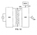
- a power supply 1202 (a Hewlett Packard model 6253A DC power supply) powered from an AC mains is connected in parallel with a capacitive element 1204 consisting of six 33 F/2.5 V aerogel super capacitors in series, each capacitor having a 5.1 k ⁇ shunt resistor, providing a total capacitance of 5.5 F and a maximum voltage of 15 V.
- the power supply 1202 and capacitive element 1204 power a switching audio amplifier 1206 (a Bose 100W switching audio amplifier, Bose Corporation) driving a speaker 1208.
- a music signal 1210 is input into amplifier 1206.
- the power supply 1202 had an output current limit set to approximately 3.2 A and a nominal output voltage (i.e., with no load) set to 15 V (for a maximum output power of 48 W), the power supply 1202 and capacitive element 1204 together provided a peak power of 98.7 W to the amplifier 1206 with the output voltage staying above 9 V for all music tested.
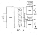
- a power supply 1302 (a DC-DC boost converter based on a Linear Technology model LTC1624 switching regulator controller) powered from six 1.2 V batteries (providing 7.2 V total input voltage) is connected in parallel with a capacitive element 1304 consisting of six 10 F/2.5 V aerogel super capacitors in series, each capacitor having a 5.1 k ⁇ shunt resistor, providing a total capacitance of 1.67 F and a maximum voltage of 15 V.
- the power supply 1302 and capacitive element 1304 power a pair of audio amplifiers 1306A and 1306B each driving a speaker 1308A and 1308B, respectively.
- Music signals 1310A and 1310B input into amplifiers 1306A and 1306B, respectively.
- the power supply 1302 had an output current limit set to approximately 0.6 A and a nominal output voltage set to 14 V (for a maximum output power of 8.4 W), the power supply 1302 and capacitive element 1304 together provided a peak power of 25.2 W to the amplifiers 1306A and 1306B with the output voltage staying above 9.5 V for all music tested.
- a power supply 1402 (a DC-DC buck converter based on a Linear Technology model LTC1624 switching regulator controller) powered from an AC mains via an AC-DC converter 1403 (an Apple Computer 12 V/1 A wall pack) is connected in parallel with a capacitive element 1404 consisting of five 4 F/2.5 V aerogel super capacitors in series, each capacitor having a 20 k ⁇ shunt resistor, providing a total capacitance of 0.8 F and a maximum voltage of 12.5 V.
- the power supply 1402 and capacitive element 1404 power a pair of audio amplifiers 1406A and 1406B each driving a speaker 1408A and 1408B, respectively.
- Music signals 1410A and 1410B input into amplifiers 1406A and 1406B, respectively.
- the power supply 1402 had an input current limit set to approximately 0.8 A and a nominal output voltage set to 12 V (for a maximum input power of 9.6 W)
- the power supply 1402 and capacitive element 1404 together provided a peak power of 25 W to the amplifiers 1406A and 1406B with the output voltage staying above the minimum operating voltage for all music tested.
Landscapes
- Engineering & Computer Science (AREA)
- Power Engineering (AREA)
- Dc-Dc Converters (AREA)
- Amplifiers (AREA)
Applications Claiming Priority (2)
| Application Number | Priority Date | Filing Date | Title |
|---|---|---|---|
| US10/872,040 US7245185B2 (en) | 2004-06-18 | 2004-06-18 | Controlling a power converter |
| US872040 | 2004-06-18 |
Publications (3)
| Publication Number | Publication Date |
|---|---|
| EP1608054A2 EP1608054A2 (en) | 2005-12-21 |
| EP1608054A3 EP1608054A3 (en) | 2006-12-13 |
| EP1608054B1 true EP1608054B1 (en) | 2015-08-12 |
Family
ID=34978712
Family Applications (1)
| Application Number | Title | Priority Date | Filing Date |
|---|---|---|---|
| EP05105040.9A Expired - Lifetime EP1608054B1 (en) | 2004-06-18 | 2005-06-09 | Controlling a power converter |
Country Status (4)
| Country | Link |
|---|---|
| US (1) | US7245185B2 (enExample) |
| EP (1) | EP1608054B1 (enExample) |
| JP (1) | JP5198724B2 (enExample) |
| CN (1) | CN100505488C (enExample) |
Families Citing this family (24)
| Publication number | Priority date | Publication date | Assignee | Title |
|---|---|---|---|---|
| US7327850B2 (en) | 2003-07-15 | 2008-02-05 | Bose Corporation | Supplying electrical power |
| US7880330B2 (en) | 2004-06-18 | 2011-02-01 | Bose Corporation | Controlling a power converter |
| US7983813B2 (en) | 2004-10-29 | 2011-07-19 | Bose Corporation | Active suspending |
| US20060244314A1 (en) * | 2005-04-27 | 2006-11-02 | Fred Graham | Hybrid power supply assembly utilizing an ultra-capacitor array |
| JP2007274812A (ja) * | 2006-03-31 | 2007-10-18 | Brother Ind Ltd | スピーカ付装置 |
| DE102006023767A1 (de) * | 2006-05-20 | 2007-11-22 | Rac Gmbh & Co. Kg | Energieversorgungssystem und Energiespeichereinheit hierfür |
| US7994756B2 (en) * | 2007-05-11 | 2011-08-09 | Nokia Corporation | Power distribution circuit for use in a portable telecommunications device |
| DE102007051944A1 (de) * | 2007-10-29 | 2009-04-30 | Egon Evertz Kg (Gmbh & Co.) | Lasthebemagnet |
| US7656061B2 (en) | 2007-10-29 | 2010-02-02 | Bose Corporation | Automatic power source configuration |
| US7888907B2 (en) * | 2007-10-30 | 2011-02-15 | Bose Corporation | Controlled charging and use of power source |
| US20090254277A1 (en) * | 2008-04-02 | 2009-10-08 | Salco Products, Inc. | Powered transmitter for railroad car applications |
| DE102008018748A1 (de) * | 2008-04-14 | 2009-10-15 | Repower Systems Ag | Windenergieanlage mit Anschlussschutzeinrichtung |
| US8338988B2 (en) * | 2009-04-17 | 2012-12-25 | Lsi Corporation | Adaptation of an active power supply set using an event trigger |
| CN101795077B (zh) * | 2010-04-12 | 2013-01-23 | Bcd半导体制造有限公司 | 一种控制变换器输出电流电压特性曲线的装置 |
| JP5519398B2 (ja) * | 2010-05-12 | 2014-06-11 | 株式会社デンソー | 電力変換装置 |
| US8581658B2 (en) * | 2011-04-08 | 2013-11-12 | Taiwan Semiconductor Manufacturing Company, Ltd. | Charge pump |
| US10447074B2 (en) | 2014-02-27 | 2019-10-15 | Hewlett Packard Enterprise Development Lp | Behavior modification of a power supply in response to a detected condition |
| US20190067958A1 (en) * | 2015-04-03 | 2019-02-28 | Charles Zimnicki | Hybrid Power Supply Unit For Audio Amplifier |
| CN109196762B (zh) * | 2016-06-02 | 2021-03-16 | 株式会社村田制作所 | 电源系统 |
| WO2019111226A1 (en) * | 2017-12-07 | 2019-06-13 | Yazami Ip Pte. Ltd. | Non-linear voltammetry-based method for charging a battery and fast charging system implementing this method |
| CN111656643B (zh) | 2017-12-07 | 2024-11-15 | 雅扎米Ip私人有限公司 | 用于对电池快速充电的自适应充电协议和实现该协议的快速充电系统 |
| KR102699043B1 (ko) * | 2019-03-21 | 2024-08-27 | 삼성전자주식회사 | 스위칭 레귤레이터 및 이를 포함하는 전자 장치 |
| CN111404371B (zh) * | 2020-02-24 | 2022-12-06 | 重庆大学 | 一种面向感性负载的高速电源系统 |
| CN114172246B (zh) * | 2022-02-10 | 2022-04-26 | 中创新航科技股份有限公司 | 一种电池、电子设备及电池的充电方法 |
Family Cites Families (15)
| Publication number | Priority date | Publication date | Assignee | Title |
|---|---|---|---|---|
| JPH01284117A (ja) * | 1988-05-11 | 1989-11-15 | Matsushita Electric Ind Co Ltd | オーディオ信号処理装置 |
| JPH0273752A (ja) * | 1988-09-09 | 1990-03-13 | Canon Inc | 電話装置 |
| FR2713842B1 (fr) | 1993-12-10 | 1996-02-23 | Csee Defense Sa | Système pour alimenter une charge en énergie électrique à partir d'une source principale et d'une source auxiliaire. |
| JP3650684B2 (ja) * | 1997-04-24 | 2005-05-25 | アイホン株式会社 | 2線式拡声インターホン装置 |
| US6104759A (en) | 1997-09-15 | 2000-08-15 | Research In Motion Limited | Power supply system for a packet-switched radio transmitter |
| US6608900B1 (en) | 1998-10-01 | 2003-08-19 | Marconi Communications, Inc. | Load management system for an electrical device |
| JP2001275271A (ja) * | 2000-03-29 | 2001-10-05 | Sony Corp | 二次電池充電装置 |
| EP1202427B1 (en) | 2000-10-27 | 2013-08-28 | Invensys Systems, Inc. | Load voltage controller for a field device and related control method |
| JP2002215248A (ja) * | 2001-01-15 | 2002-07-31 | Sony Corp | 電源回路 |
| US6580945B2 (en) | 2001-03-20 | 2003-06-17 | Koninklijke Philips Electronics N.V. | Defibrillator using low impedance high capacitance double layer capacitor |
| FR2826202B1 (fr) | 2001-06-18 | 2003-12-19 | Cit Alcatel | Procede et dispositif d'equilibrage de supercapacite |
| US6628107B1 (en) | 2001-10-31 | 2003-09-30 | Symbol Technologies, Inc. | Power management for a portable electronic device |
| US6653814B1 (en) | 2002-06-28 | 2003-11-25 | Motorola Inc. | Method for determining power supply compatibility in a portable device |
| DE10255330A1 (de) | 2002-11-27 | 2004-06-17 | Robert Bosch Gmbh | Verfahren zur Einstellung der Versorungsspannung für eine Verstärkerstufe und Verstärkeranordnung |
| US6949915B2 (en) * | 2003-07-24 | 2005-09-27 | Harman International Industries, Incorporated | Opposed current converter power factor correcting power supply |
-
2004
- 2004-06-18 US US10/872,040 patent/US7245185B2/en not_active Expired - Fee Related
-
2005
- 2005-06-09 EP EP05105040.9A patent/EP1608054B1/en not_active Expired - Lifetime
- 2005-06-16 JP JP2005176844A patent/JP5198724B2/ja not_active Expired - Fee Related
- 2005-06-20 CN CNB2005100783924A patent/CN100505488C/zh not_active Expired - Fee Related
Also Published As
| Publication number | Publication date |
|---|---|
| JP2006006098A (ja) | 2006-01-05 |
| US7245185B2 (en) | 2007-07-17 |
| HK1084249A1 (zh) | 2006-07-21 |
| EP1608054A3 (en) | 2006-12-13 |
| EP1608054A2 (en) | 2005-12-21 |
| CN1722587A (zh) | 2006-01-18 |
| JP5198724B2 (ja) | 2013-05-15 |
| US20050280312A1 (en) | 2005-12-22 |
| CN100505488C (zh) | 2009-06-24 |
Similar Documents
| Publication | Publication Date | Title |
|---|---|---|
| EP1608054B1 (en) | Controlling a power converter | |
| US7880330B2 (en) | Controlling a power converter | |
| US7888907B2 (en) | Controlled charging and use of power source | |
| US7656061B2 (en) | Automatic power source configuration | |
| US7777459B2 (en) | High-efficiency DC/DC voltage converter including capacitive switching pre-converter and down inductive switching post-regulator | |
| JP3697696B2 (ja) | Dc−dcコンバータ | |
| US7368897B2 (en) | Load adaptive power converter | |
| KR20030011078A (ko) | 발진기 없는 dc-dc 전력 변환기 | |
| JP2003528558A (ja) | ウルトラキャパシタによる動的調整チャージポンプ式電力コンバータ | |
| Kim et al. | Ripple feedback filter suitable for analog/digital mixed-mode audio amplifier for improved efficiency and stability | |
| JP2003528560A (ja) | 動的に制御され固有に調整されるチャージポンプ電力コンバータ | |
| JP2006296198A (ja) | 動的切換可能な電力変換器 | |
| US8797010B2 (en) | Startup for DC/DC converters | |
| TWI779997B (zh) | 固定時間升降壓切換式轉換器及調變控制電路與控制方法 | |
| CN101997411B (zh) | 升降压式电源转换器的控制电路及方法 | |
| Cid-Pastor et al. | Analysis and design of power gyrators in sliding-mode operation | |
| TW201108577A (en) | Methods for light load efficiency improvement of a buck boost voltage regulater | |
| US11594954B2 (en) | Soft start method for a single inductor multiple output power supply | |
| CN116526821B (zh) | 芯片、直流-直流电路及其控制方法 | |
| HK1084249B (en) | Controlling a power converter | |
| US5548501A (en) | High-voltage power supply circuit with a voltage discharging circuit | |
| JP3697252B2 (ja) | 直流−直流変換制御回路および直流−直流変換装置 | |
| CN102005922B (zh) | 改善升降压式电压调节器的轻载效率的方法 | |
| US20240413800A1 (en) | Current limit for charge pump boost driven class d audio amplifier | |
| KR20240001889A (ko) | 벅-부스트 컨버터 |
Legal Events
| Date | Code | Title | Description |
|---|---|---|---|
| PUAI | Public reference made under article 153(3) epc to a published international application that has entered the european phase |
Free format text: ORIGINAL CODE: 0009012 |
|
| AK | Designated contracting states |
Kind code of ref document: A2 Designated state(s): AT BE BG CH CY CZ DE DK EE ES FI FR GB GR HU IE IS IT LI LT LU MC NL PL PT RO SE SI SK TR |
|
| AX | Request for extension of the european patent |
Extension state: AL BA HR LV MK YU |
|
| PUAL | Search report despatched |
Free format text: ORIGINAL CODE: 0009013 |
|
| AK | Designated contracting states |
Kind code of ref document: A3 Designated state(s): AT BE BG CH CY CZ DE DK EE ES FI FR GB GR HU IE IS IT LI LT LU MC NL PL PT RO SE SI SK TR |
|
| AX | Request for extension of the european patent |
Extension state: AL BA HR LV MK YU |
|
| 17P | Request for examination filed |
Effective date: 20070604 |
|
| AKX | Designation fees paid |
Designated state(s): AT BE BG CH CY CZ DE DK EE ES FI FR GB GR HU IE IS IT LI LT LU MC NL PL PT RO SE SI SK TR |
|
| 17Q | First examination report despatched |
Effective date: 20070928 |
|
| REG | Reference to a national code |
Ref country code: DE Ref legal event code: R079 Ref document number: 602005047195 Country of ref document: DE Free format text: PREVIOUS MAIN CLASS: H02M0003155000 Ipc: H02M0003156000 |
|
| GRAP | Despatch of communication of intention to grant a patent |
Free format text: ORIGINAL CODE: EPIDOSNIGR1 |
|
| RIC1 | Information provided on ipc code assigned before grant |
Ipc: H02M 3/156 20060101AFI20150120BHEP Ipc: H02J 7/34 20060101ALI20150120BHEP |
|
| INTG | Intention to grant announced |
Effective date: 20150224 |
|
| GRAS | Grant fee paid |
Free format text: ORIGINAL CODE: EPIDOSNIGR3 |
|
| GRAA | (expected) grant |
Free format text: ORIGINAL CODE: 0009210 |
|
| AK | Designated contracting states |
Kind code of ref document: B1 Designated state(s): AT BE BG CH CY CZ DE DK EE ES FI FR GB GR HU IE IS IT LI LT LU MC NL PL PT RO SE SI SK TR |
|
| REG | Reference to a national code |
Ref country code: GB Ref legal event code: FG4D |
|
| REG | Reference to a national code |
Ref country code: CH Ref legal event code: EP |
|
| REG | Reference to a national code |
Ref country code: AT Ref legal event code: REF Ref document number: 742914 Country of ref document: AT Kind code of ref document: T Effective date: 20150815 |
|
| REG | Reference to a national code |
Ref country code: IE Ref legal event code: FG4D |
|
| REG | Reference to a national code |
Ref country code: DE Ref legal event code: R096 Ref document number: 602005047195 Country of ref document: DE |
|
| REG | Reference to a national code |
Ref country code: LT Ref legal event code: MG4D |
|
| REG | Reference to a national code |
Ref country code: AT Ref legal event code: MK05 Ref document number: 742914 Country of ref document: AT Kind code of ref document: T Effective date: 20150812 |
|
| REG | Reference to a national code |
Ref country code: NL Ref legal event code: MP Effective date: 20150812 |
|
| PG25 | Lapsed in a contracting state [announced via postgrant information from national office to epo] |
Ref country code: FI Free format text: LAPSE BECAUSE OF FAILURE TO SUBMIT A TRANSLATION OF THE DESCRIPTION OR TO PAY THE FEE WITHIN THE PRESCRIBED TIME-LIMIT Effective date: 20150812 Ref country code: LT Free format text: LAPSE BECAUSE OF FAILURE TO SUBMIT A TRANSLATION OF THE DESCRIPTION OR TO PAY THE FEE WITHIN THE PRESCRIBED TIME-LIMIT Effective date: 20150812 Ref country code: GR Free format text: LAPSE BECAUSE OF FAILURE TO SUBMIT A TRANSLATION OF THE DESCRIPTION OR TO PAY THE FEE WITHIN THE PRESCRIBED TIME-LIMIT Effective date: 20151113 |
|
| PG25 | Lapsed in a contracting state [announced via postgrant information from national office to epo] |
Ref country code: SE Free format text: LAPSE BECAUSE OF FAILURE TO SUBMIT A TRANSLATION OF THE DESCRIPTION OR TO PAY THE FEE WITHIN THE PRESCRIBED TIME-LIMIT Effective date: 20150812 Ref country code: ES Free format text: LAPSE BECAUSE OF FAILURE TO SUBMIT A TRANSLATION OF THE DESCRIPTION OR TO PAY THE FEE WITHIN THE PRESCRIBED TIME-LIMIT Effective date: 20150812 Ref country code: AT Free format text: LAPSE BECAUSE OF FAILURE TO SUBMIT A TRANSLATION OF THE DESCRIPTION OR TO PAY THE FEE WITHIN THE PRESCRIBED TIME-LIMIT Effective date: 20150812 Ref country code: PL Free format text: LAPSE BECAUSE OF FAILURE TO SUBMIT A TRANSLATION OF THE DESCRIPTION OR TO PAY THE FEE WITHIN THE PRESCRIBED TIME-LIMIT Effective date: 20150812 Ref country code: PT Free format text: LAPSE BECAUSE OF FAILURE TO SUBMIT A TRANSLATION OF THE DESCRIPTION OR TO PAY THE FEE WITHIN THE PRESCRIBED TIME-LIMIT Effective date: 20151214 Ref country code: IS Free format text: LAPSE BECAUSE OF FAILURE TO SUBMIT A TRANSLATION OF THE DESCRIPTION OR TO PAY THE FEE WITHIN THE PRESCRIBED TIME-LIMIT Effective date: 20151212 |
|
| PG25 | Lapsed in a contracting state [announced via postgrant information from national office to epo] |
Ref country code: NL Free format text: LAPSE BECAUSE OF FAILURE TO SUBMIT A TRANSLATION OF THE DESCRIPTION OR TO PAY THE FEE WITHIN THE PRESCRIBED TIME-LIMIT Effective date: 20150812 |
|
| PG25 | Lapsed in a contracting state [announced via postgrant information from national office to epo] |
Ref country code: CZ Free format text: LAPSE BECAUSE OF FAILURE TO SUBMIT A TRANSLATION OF THE DESCRIPTION OR TO PAY THE FEE WITHIN THE PRESCRIBED TIME-LIMIT Effective date: 20150812 Ref country code: EE Free format text: LAPSE BECAUSE OF FAILURE TO SUBMIT A TRANSLATION OF THE DESCRIPTION OR TO PAY THE FEE WITHIN THE PRESCRIBED TIME-LIMIT Effective date: 20150812 Ref country code: DK Free format text: LAPSE BECAUSE OF FAILURE TO SUBMIT A TRANSLATION OF THE DESCRIPTION OR TO PAY THE FEE WITHIN THE PRESCRIBED TIME-LIMIT Effective date: 20150812 Ref country code: IT Free format text: LAPSE BECAUSE OF FAILURE TO SUBMIT A TRANSLATION OF THE DESCRIPTION OR TO PAY THE FEE WITHIN THE PRESCRIBED TIME-LIMIT Effective date: 20150812 Ref country code: SK Free format text: LAPSE BECAUSE OF FAILURE TO SUBMIT A TRANSLATION OF THE DESCRIPTION OR TO PAY THE FEE WITHIN THE PRESCRIBED TIME-LIMIT Effective date: 20150812 |
|
| REG | Reference to a national code |
Ref country code: DE Ref legal event code: R097 Ref document number: 602005047195 Country of ref document: DE |
|
| PG25 | Lapsed in a contracting state [announced via postgrant information from national office to epo] |
Ref country code: RO Free format text: LAPSE BECAUSE OF FAILURE TO SUBMIT A TRANSLATION OF THE DESCRIPTION OR TO PAY THE FEE WITHIN THE PRESCRIBED TIME-LIMIT Effective date: 20150812 |
|
| PLBE | No opposition filed within time limit |
Free format text: ORIGINAL CODE: 0009261 |
|
| STAA | Information on the status of an ep patent application or granted ep patent |
Free format text: STATUS: NO OPPOSITION FILED WITHIN TIME LIMIT |
|
| REG | Reference to a national code |
Ref country code: FR Ref legal event code: PLFP Year of fee payment: 12 |
|
| 26N | No opposition filed |
Effective date: 20160513 |
|
| PGFP | Annual fee paid to national office [announced via postgrant information from national office to epo] |
Ref country code: GB Payment date: 20160627 Year of fee payment: 12 |
|
| PG25 | Lapsed in a contracting state [announced via postgrant information from national office to epo] |
Ref country code: SI Free format text: LAPSE BECAUSE OF FAILURE TO SUBMIT A TRANSLATION OF THE DESCRIPTION OR TO PAY THE FEE WITHIN THE PRESCRIBED TIME-LIMIT Effective date: 20150812 |
|
| PGFP | Annual fee paid to national office [announced via postgrant information from national office to epo] |
Ref country code: FR Payment date: 20160628 Year of fee payment: 12 |
|
| PGFP | Annual fee paid to national office [announced via postgrant information from national office to epo] |
Ref country code: DE Payment date: 20160628 Year of fee payment: 12 |
|
| PG25 | Lapsed in a contracting state [announced via postgrant information from national office to epo] |
Ref country code: BE Free format text: LAPSE BECAUSE OF FAILURE TO SUBMIT A TRANSLATION OF THE DESCRIPTION OR TO PAY THE FEE WITHIN THE PRESCRIBED TIME-LIMIT Effective date: 20150812 |
|
| PG25 | Lapsed in a contracting state [announced via postgrant information from national office to epo] |
Ref country code: MC Free format text: LAPSE BECAUSE OF FAILURE TO SUBMIT A TRANSLATION OF THE DESCRIPTION OR TO PAY THE FEE WITHIN THE PRESCRIBED TIME-LIMIT Effective date: 20150812 |
|
| REG | Reference to a national code |
Ref country code: CH Ref legal event code: PL |
|
| REG | Reference to a national code |
Ref country code: IE Ref legal event code: MM4A |
|
| PG25 | Lapsed in a contracting state [announced via postgrant information from national office to epo] |
Ref country code: LI Free format text: LAPSE BECAUSE OF NON-PAYMENT OF DUE FEES Effective date: 20160630 Ref country code: CH Free format text: LAPSE BECAUSE OF NON-PAYMENT OF DUE FEES Effective date: 20160630 |
|
| PG25 | Lapsed in a contracting state [announced via postgrant information from national office to epo] |
Ref country code: IE Free format text: LAPSE BECAUSE OF NON-PAYMENT OF DUE FEES Effective date: 20160609 |
|
| REG | Reference to a national code |
Ref country code: DE Ref legal event code: R119 Ref document number: 602005047195 Country of ref document: DE |
|
| GBPC | Gb: european patent ceased through non-payment of renewal fee |
Effective date: 20170609 |
|
| REG | Reference to a national code |
Ref country code: FR Ref legal event code: ST Effective date: 20180228 |
|
| PG25 | Lapsed in a contracting state [announced via postgrant information from national office to epo] |
Ref country code: GB Free format text: LAPSE BECAUSE OF NON-PAYMENT OF DUE FEES Effective date: 20170609 Ref country code: DE Free format text: LAPSE BECAUSE OF NON-PAYMENT OF DUE FEES Effective date: 20180103 |
|
| PG25 | Lapsed in a contracting state [announced via postgrant information from national office to epo] |
Ref country code: HU Free format text: LAPSE BECAUSE OF FAILURE TO SUBMIT A TRANSLATION OF THE DESCRIPTION OR TO PAY THE FEE WITHIN THE PRESCRIBED TIME-LIMIT; INVALID AB INITIO Effective date: 20050609 Ref country code: CY Free format text: LAPSE BECAUSE OF FAILURE TO SUBMIT A TRANSLATION OF THE DESCRIPTION OR TO PAY THE FEE WITHIN THE PRESCRIBED TIME-LIMIT Effective date: 20150812 Ref country code: FR Free format text: LAPSE BECAUSE OF NON-PAYMENT OF DUE FEES Effective date: 20170630 |
|
| PG25 | Lapsed in a contracting state [announced via postgrant information from national office to epo] |
Ref country code: TR Free format text: LAPSE BECAUSE OF FAILURE TO SUBMIT A TRANSLATION OF THE DESCRIPTION OR TO PAY THE FEE WITHIN THE PRESCRIBED TIME-LIMIT Effective date: 20150812 Ref country code: LU Free format text: LAPSE BECAUSE OF NON-PAYMENT OF DUE FEES Effective date: 20160609 |
|
| PG25 | Lapsed in a contracting state [announced via postgrant information from national office to epo] |
Ref country code: BG Free format text: LAPSE BECAUSE OF FAILURE TO SUBMIT A TRANSLATION OF THE DESCRIPTION OR TO PAY THE FEE WITHIN THE PRESCRIBED TIME-LIMIT Effective date: 20150812 |