EP1607782A2 - Solid-state imaging device and manufacturing method thereof, and camera module - Google Patents
Solid-state imaging device and manufacturing method thereof, and camera module Download PDFInfo
- Publication number
- EP1607782A2 EP1607782A2 EP05253677A EP05253677A EP1607782A2 EP 1607782 A2 EP1607782 A2 EP 1607782A2 EP 05253677 A EP05253677 A EP 05253677A EP 05253677 A EP05253677 A EP 05253677A EP 1607782 A2 EP1607782 A2 EP 1607782A2
- Authority
- EP
- European Patent Office
- Prior art keywords
- imaging device
- transparent substrate
- solid state
- filter layer
- optical filter
- Prior art date
- Legal status (The legal status is an assumption and is not a legal conclusion. Google has not performed a legal analysis and makes no representation as to the accuracy of the status listed.)
- Withdrawn
Links
Images




Classifications
-
- G—PHYSICS
- G02—OPTICS
- G02B—OPTICAL ELEMENTS, SYSTEMS OR APPARATUS
- G02B7/00—Mountings, adjusting means, or light-tight connections, for optical elements
- G02B7/02—Mountings, adjusting means, or light-tight connections, for optical elements for lenses
-
- H—ELECTRICITY
- H10—SEMICONDUCTOR DEVICES; ELECTRIC SOLID-STATE DEVICES NOT OTHERWISE PROVIDED FOR
- H10F—INORGANIC SEMICONDUCTOR DEVICES SENSITIVE TO INFRARED RADIATION, LIGHT, ELECTROMAGNETIC RADIATION OF SHORTER WAVELENGTH OR CORPUSCULAR RADIATION
- H10F39/00—Integrated devices, or assemblies of multiple devices, comprising at least one element covered by group H10F30/00, e.g. radiation detectors comprising photodiode arrays
- H10F39/10—Integrated devices
- H10F39/12—Image sensors
-
- G—PHYSICS
- G02—OPTICS
- G02B—OPTICAL ELEMENTS, SYSTEMS OR APPARATUS
- G02B13/00—Optical objectives specially designed for the purposes specified below
- G02B13/001—Miniaturised objectives for electronic devices, e.g. portable telephones, webcams, PDAs, small digital cameras
- G02B13/008—Miniaturised objectives for electronic devices, e.g. portable telephones, webcams, PDAs, small digital cameras designed for infrared light
-
- H—ELECTRICITY
- H04—ELECTRIC COMMUNICATION TECHNIQUE
- H04N—PICTORIAL COMMUNICATION, e.g. TELEVISION
- H04N23/00—Cameras or camera modules comprising electronic image sensors; Control thereof
- H04N23/50—Constructional details
- H04N23/54—Mounting of pick-up tubes, electronic image sensors, deviation or focusing coils
-
- H—ELECTRICITY
- H10—SEMICONDUCTOR DEVICES; ELECTRIC SOLID-STATE DEVICES NOT OTHERWISE PROVIDED FOR
- H10F—INORGANIC SEMICONDUCTOR DEVICES SENSITIVE TO INFRARED RADIATION, LIGHT, ELECTROMAGNETIC RADIATION OF SHORTER WAVELENGTH OR CORPUSCULAR RADIATION
- H10F39/00—Integrated devices, or assemblies of multiple devices, comprising at least one element covered by group H10F30/00, e.g. radiation detectors comprising photodiode arrays
- H10F39/011—Manufacture or treatment of image sensors covered by group H10F39/12
- H10F39/026—Wafer-level processing
-
- H—ELECTRICITY
- H10—SEMICONDUCTOR DEVICES; ELECTRIC SOLID-STATE DEVICES NOT OTHERWISE PROVIDED FOR
- H10F—INORGANIC SEMICONDUCTOR DEVICES SENSITIVE TO INFRARED RADIATION, LIGHT, ELECTROMAGNETIC RADIATION OF SHORTER WAVELENGTH OR CORPUSCULAR RADIATION
- H10F39/00—Integrated devices, or assemblies of multiple devices, comprising at least one element covered by group H10F30/00, e.g. radiation detectors comprising photodiode arrays
- H10F39/80—Constructional details of image sensors
- H10F39/804—Containers or encapsulations
-
- H—ELECTRICITY
- H10—SEMICONDUCTOR DEVICES; ELECTRIC SOLID-STATE DEVICES NOT OTHERWISE PROVIDED FOR
- H10F—INORGANIC SEMICONDUCTOR DEVICES SENSITIVE TO INFRARED RADIATION, LIGHT, ELECTROMAGNETIC RADIATION OF SHORTER WAVELENGTH OR CORPUSCULAR RADIATION
- H10F39/00—Integrated devices, or assemblies of multiple devices, comprising at least one element covered by group H10F30/00, e.g. radiation detectors comprising photodiode arrays
- H10F39/80—Constructional details of image sensors
- H10F39/806—Optical elements or arrangements associated with the image sensors
- H10F39/8063—Microlenses
-
- H—ELECTRICITY
- H10—SEMICONDUCTOR DEVICES; ELECTRIC SOLID-STATE DEVICES NOT OTHERWISE PROVIDED FOR
- H10F—INORGANIC SEMICONDUCTOR DEVICES SENSITIVE TO INFRARED RADIATION, LIGHT, ELECTROMAGNETIC RADIATION OF SHORTER WAVELENGTH OR CORPUSCULAR RADIATION
- H10F77/00—Constructional details of devices covered by this subclass
- H10F77/40—Optical elements or arrangements
- H10F77/407—Optical elements or arrangements indirectly associated with the devices
-
- H—ELECTRICITY
- H04—ELECTRIC COMMUNICATION TECHNIQUE
- H04N—PICTORIAL COMMUNICATION, e.g. TELEVISION
- H04N23/00—Cameras or camera modules comprising electronic image sensors; Control thereof
- H04N23/50—Constructional details
- H04N23/55—Optical parts specially adapted for electronic image sensors; Mounting thereof
-
- H—ELECTRICITY
- H10—SEMICONDUCTOR DEVICES; ELECTRIC SOLID-STATE DEVICES NOT OTHERWISE PROVIDED FOR
- H10F—INORGANIC SEMICONDUCTOR DEVICES SENSITIVE TO INFRARED RADIATION, LIGHT, ELECTROMAGNETIC RADIATION OF SHORTER WAVELENGTH OR CORPUSCULAR RADIATION
- H10F39/00—Integrated devices, or assemblies of multiple devices, comprising at least one element covered by group H10F30/00, e.g. radiation detectors comprising photodiode arrays
- H10F39/80—Constructional details of image sensors
- H10F39/805—Coatings
- H10F39/8053—Colour filters
-
- H—ELECTRICITY
- H10—SEMICONDUCTOR DEVICES; ELECTRIC SOLID-STATE DEVICES NOT OTHERWISE PROVIDED FOR
- H10W—GENERIC PACKAGES, INTERCONNECTIONS, CONNECTORS OR OTHER CONSTRUCTIONAL DETAILS OF DEVICES COVERED BY CLASS H10
- H10W90/00—Package configurations
- H10W90/701—Package configurations characterised by the relative positions of pads or connectors relative to package parts
- H10W90/751—Package configurations characterised by the relative positions of pads or connectors relative to package parts of bond wires
- H10W90/754—Package configurations characterised by the relative positions of pads or connectors relative to package parts of bond wires between a chip and a stacked insulating package substrate, interposer or RDL
Definitions
- the present invention relates to improvements on a solid state imaging device for converting optical images into image signals, a manufacturing method for the solid state imaging device, and a camera module which employs the solid state imaging device.
- a popular type of the solid state imaging devices includes a solid state imaging chip (or bare chip), a ceramic package for accommodating the solid state imaging chip, and a transparent cover glass for sealing the package.
- On the solid state imaging chip plural electrode pads are provided. Connecting these electrode pads to inner connection terminals of the package by wire bonding, then bonding outer connection terminals of the package on a mounting board will establish an electrical connection of the imaging chip to a circuit in the mounting board.
- the solid state imaging devices are also employed in portable electronic apparatuses such as cellular phones and electronic agendas (or personal digital assistances), providing them with an image pickup function.
- portable electronic apparatuses such as cellular phones and electronic agendas (or personal digital assistances), providing them with an image pickup function.
- an image pickup function there is a unitized camera module in which the solid state imaging device, an optical unit with an image pickup optical system, and a mounting board with a control circuit are put together.
- Fig.12 shows a conventional camera module which employs a ceramic package type solid state imaging device 41.
- This camera module is composed of the solid state imaging device 41, an optical unit 48, and a mounting board 47.
- the solid state imaging device 41 is constituted of a solid state imaging chip 44, a package 45 for accommodating the solid state imaging chip 44, and a cover glass 46 for sealing the package 45, and is attached on the mounting board 47.
- the solid state imaging chip 44 is configured with a semiconductor substrate 42 with an imaging section 42a, which has plural pixels arranged in a matrix, and a microlens array 43 attached on the imaging section 42a.
- the optical unit 48 includes a housing portion 48a for accommodating the solid state image device 41 and a lens barrel 48b to hold a taking lens 49, and is fixed to the mounting board 47.
- the above camera module uses an infrared cut filter 52 and an optical low pass filter 53 to improve image quality.
- an anti-reflection filter 54 may be attached on the upper surface of the cover glass 46 to prevent the incident light reflecting diffusely inside the solid state imaging device 41. Since these infrared cut filter 52 and optical low pass filter 53 are placed between the solid state imaging device 41 and the taking lens 49 in the optical unit 48, their attachment spaces cause the camera module to grow in size.
- One solution to this problem is indicated in the Japanese patent laid-open publication No.2004-064272, which discloses a solid state imaging device with a sheet of infrared cut filter on the cover glass.
- the solid state imaging devices are , in addition, preferred to be small in order to reduce the size of the portable electronic apparatuses.
- the Japanese patent laid-open publication No.2002-231921 discloses a solid state imaging device using a wafer level chip size package (hereinafter referred to as WLCSP) which is packaged on a wafer.
- WLCSP wafer level chip size package
- the applicant has filed US Serial No.10/839,231 for a camera module which employs the WLCSP type solid state imaging device on the date of May 6, 2004.
- the WLCSP type solid state imaging device is as small as the bare chip, and is composed of a semiconductor substrate with a microlens array and a cover glass attached to the semiconductor substrate for protection of imaging elements in the solid state imaging device. With the outer dimension of a few millimeters square, such a small WLCSP type imaging device makes it very difficult to attach the filters on the cover glass.
- a primary object of the present invention is to offer an optical filter layer formed on the cover glass of the WLCSP type solid state imaging device at low cost.
- a large filter layer is formed on a transparent substrate before cutting a substrate assembly into individual imaging devices.
- the transparent substrate is attached to a substrate wafer, on which a plurality of imaging sections are formed, with keeping a predetermined gap created by a spacer surrounding each of the image sections.
- the optical filter layer is composed of optical filter plates or sheets attached on the transparent substrate, or of optical filter films deposited on the transparent substrate, and includes an infrared cut filter, an optical low pass filter, an anti-reflection filter and some such.
- a manufacturing method for the solid state imaging device of the present invention includes a forming step of the optical filter layer on the surface of the transparent substrate, an attaching process of the transparent substrate to the semiconductor wafer having a plurality of imaging sections, and a cutting process of the transparent substrate and the semiconductor wafer along each of the imaging sections.
- the optical filter layer is formed on the surface of the transparent substrate after the transparent substrate is attached to the semiconductor wafer with a plurality of imaging sections.
- the forming step of the optical filter layer is made by attaching optical filter plates or sheets to the transparent substrate.
- a camera module of the present invention is provided with a circuit board, an optical unit, and the imaging device.
- the imaging device is placed inside the optical unit, and the optical unit is attached to the circuit board together with the imaging device.
- an imaging section on a semiconductor substrate is packaged by a transparent substrate with keeping a predetermined gap created by a spacer.
- the semiconductor substrate and the transparent cover are formed by dicing both the semiconductor wafer having a plurality of imaging sections thereon and the transparent substrate having an optical filter layer.
- the optical filter layer can be formed on the cover glass of the WLCSP type solid state imaging device which has the outside dimension of as small as a few millimeters square. This configuration enables to downsize the camera module and, eventually, contributes to downsize the portable electronic apparatuses which incorporate the aforesaid camera module.
- the optical filter layer on the cover glass surface can be the infrared cut filter, the optical low pass filter, the anti-reflection filter and some such, and besides, it can be made either by attaching or depositing. It is therefore possible to select an appropriate combination of kind and process in forming the optical filter layer according to performance and purpose of the solid state imaging device and the camera module.
- a camera module 2 comprises a solid state imaging device 3, a mounting board 4 to the solid state imaging device 3, and an optical unit 6 attached to the mounting board 4.
- the optical unit 6 has a taking lens 5 placed above the solid state imaging device 3.
- the solid state imaging device 3 is composed of an imaging chip 8, a spacer 11, a cover glass 12, and an optical filter layer formed on the cover glass 12.
- the optical filter layer includes at least an infrared cut filter layer 13 and an optical low pass filter layer 14.
- the imaging chip 8 is constituted of a semiconductor substrate 10 and a microlens array 9.
- the semiconductor substrate 10 is a chip diced off a silicon wafer, and an imaging section 10a is formed thereon.
- the imaging section 10a includes plural pixels arranged in a matrix, each of which pixels has a photoelectric conversion function and an electric charge accumulation function.
- the embodiment uses a CCD type imaging section which is composed of photodiodes and charge-coupled devices (CCD), however, a MOS type imaging section composed of photodiodes and MOS switches can also be used.
- a mosaic filter is attached on the imaging section 10a so that one of a red section, a green section, or a blue section of the mosaic filter is located immediately above its corresponding pixel.
- the microlens array 9 is attached on the mosaic filter such that individual microlens agrees in position with each of the pixels.
- the spacer 11 has a square shape with an opening 17 in the middle, and is attached to an upper surface of the semiconductor substrate 10 so as to enclose the imaging section 10a.
- the spacer 11 is made from inorganic material such as a silicon or the like. Creating a gap between the microlens array 9 and the cover glass (i.e. transparent cover) 12, the spacer 11 prevents the physical contact of microlens array 9 with the cover glass 12.
- the cover glass 12 is attached to the upper surface of the spacer 11 to cover the opening 17.
- the cover glass 12 is also made of a low alpha-ray emission glass, protecting each pixel of the imaging section 10a from being destroyed by an alpha-ray.
- outer connection terminals 20 are provided outside the spacer 11 on the semiconductor substrate 10.
- the outer connection terminals 20 are linked to the imaging section 10a through wiring on the surface of the semiconductor substrate 10.
- the outer connection terminals 20 are connected by wire bonding to the mounting board 4.
- the infrared cut filter layer 13 and the optical low pass filter layer 14 improve quality of the images captured with the solid state imaging device 3.
- the infrared cut filter layer 13 blocks the infrared ray within a particular wavelength range, eliminating ghost images and fog by the infrared light.
- the optical low pass filter layer 14 blocks high frequency components in the spatial frequency, eliminating false color and moire effects. Because the infrared cut filter layer 13 and the optical low pass filter layer 14 are bonded on the cover glass 12, the optical unit 6 need not have the attachment space dedicated for them, and the camera module 2 can thereby be downsized. Further, an anti-reflection filter layer may also be provided on the lower or upper surface of the cover glass 12 to prevent the incident light reflecting diffusely inside the solid state imaging device 3.
- the mounting board 4 is a rigid board, made of a glass epoxy board or a ceramic board, and is attached to both the solid state imaging device 3 and the optical unit 6.
- the mounting board 4 is provided with a drive circuit for the solid state imaging device 3.
- the optical unit 6 comprises the taking lens 5 and a lens holder 23.
- the lens holder 23 includes a boxy base portion 23a to be attached to the mounting board 4 to cover the solid state imaging device 3 and a cylindrical lens barrel 23b to hold the taking lens 5.
- the optical filter layer is formed on a glass substrate 26, which is the base material of the cover glass 12.
- the optical filter layer is formed by bonding an infrared cut filter substrate 27 and an optical low pass filter substrate 28 to the glass substrate 26 with an adhesive agent 29.
- the infrared cut filter substrate 27 and the optical low pass filter substrate 28 are about the same size as the glass substrate 26.
- the adhesive agent 29 may be a ultraviolet adhesive, which turns into transparency after hardening.
- the adhesive agent 29 is spread, with uniform thickness, on the entire surface of the glass substrate 26.
- the glass substrate 26 is attached to the infrared cut filter substrate 27 under, for example, the vacuum environment. After attachment, one of the glass substrate 26 and the infrared cut filter substrate 27 is sucked with vacuum while the other is pressed with air pressure so that they stick to each other firmly. Subsequent ultraviolet irradiation through the glass substrate 26 hardens the adhesive agent 29, hence the glass substrate 26 and the infrared cut filter substrate 27 are put together tightly.
- the same attachment procedure as above applies to the optical low pass filter substrate 28 onto the infrared cut filter substrate 27, and its detailed explanation is omitted.
- a plurality of the spacers 11 are formed on the lower surface of the glass substrate 26.
- the spacer 11 is formed under the following procedure. Firstly, a silicon wafer for the spacer is attached on the lower surface of the glass substrate 26 with an adhesive agent. Secondly, a resist mask in the shape of the spacer 11 is formed on the silicon wafer by photolithography. Lastly, the portions without the resist mask are removed by plasma etching to form pluralities of the spacers 11 on the glass substrate 26. After the etching, the remaining resist mask on the silicon wafer is removed by ashing or the like.
- Fig.5C and Fig. 6 show the third process, in which the glass substrate 26 and a semiconductor wafer 32 are attached together with an adhesive agent. Formed in the semiconductor wafer 32 are a plurality of the imaging sections 10a, on each of which the microlens arrays 9 are attached.
- an alignment and bonding apparatus will be used. The alignment and bonding apparatus performs face to face alignment of the glass substrate 26 and the semiconductor wafer 32, with reference to their respective orientation flats 26a and 32a, in the XY and the rotation directions. Stacked and compressed by the alignment and bonding apparatus thereafter, the glass substrate 26 and the semiconductor wafer 32 are attached together with the adhesive agent to form a substrate assembly. Upon this attachment, each of the microlens arrays 9 is sealed by the spacer 11 and the glass substrate 26 on the semiconductor wafer 32, protected from dust in the subsequent processes.
- Fig.5D shows the fourth process, in which the glass substrate 26, the infrared cut filter substrate 27 and the optical low pass filter substrate 28 both attached to the glass substrate 26, and the semiconductor wafer 32 are diced all together.
- the substrate assembly is placed on a dicing machine with a dicing tape adhering to the glass substrate 26.
- the dicing machine cuts off the glass substrate 26, the infrared cut filter substrate 27, the optical low pass filter substrate 28, and the semiconductor wafer 32 along each solid state imaging device 3 with using, for example, a metal resin grinding wheel which is made from diamond abrasive grains bonded with a resin.
- the infrared cut filter layer 13 and the optical low pass filter layer 14 are attached to the glass substrate 26 before the glass substrate 26 and the semiconductor wafer 32 are diced together. This method only necessitates a single attaching process of the optical filter, and the manufacturing cost and the process steps are therefore reduced significantly.
- the completed solid state imaging device 3 undergoes functional tests, and is attached to the mounting board 4 together with the optical unit 6 to compose the camera module 2.
- the camera module 2 is incorporated in the portable electronic apparatuses such as cellular phones or the like. With the infrared cut filter layer 13 and the optical low pass filter layer 14 formed on the cover glass 12 of the solid state and the optical low pass filter imaging device 3, the camera module 2 of this embodiment is able to downsize the optical unit 6 and, in fact, contributes to further downsizing of the portable electronic apparatuses which incorporate the camera module 2.
- the optical filter layer is formed by attaching the sheet-like or plate-like infrared cut filter substrate 27 and optical low pass filter substrate 28 to the glass substrate 26 in the above embodiment, it is also possible to deposit films of an infrared cut filter layer 35 and an optical low pass filter layer 36 on a cover glass 35, as a solid state imaging device 34 shown in Fig.7.
- the optical filter layers are formed on a glass substrate 38, which is the base material of the cover glass 35, by means of a CVD (chemical vapor deposition) machine, a vacuum vapor deposition machine or the like.
- CVD chemical vapor deposition
- a vacuum vapor deposition machine or the like.
- the optical filter layer is formed on the glass substrate before the glass substrate is attached to the semiconductor wafer.
- the glass substrate may, however, be attached to the semiconductor wafer before the optical filter layer is formed on the glass substrate by attaching or depositing films.
- a solid state imaging device 60 shown in Fig.9 is provided with an anti-reflection filter layer 63 on the confronting surface of the cover glass 61 with a microlens array 62 in order to prevent the incident light reflecting diffusely inside the solid state imaging device 60.
- the anti-reflection filter layer 63 is formed on a surface of a glass substrate 65, which is the base material of the cover glass 61, by such a film deposition method as the CVD or the vacuum vapor deposition. And a plurality of spacers 67 are formed on the anti-reflection filter layer 63 as shown in Fig.10B. Then, as shown in Fig.10C, the glass substrate 65 is attached to a semiconductor wafer 68. Meanwhile, the semiconductor wafer 68 has the same configuration as the semiconductor wafer 32 shown in Fig.5C, and its detailed explanation will be omitted.
- the glass substrate 65 and the semiconductor wafer 68 are diced along each of the microlens arrays 62.
- This method provides the solid state imaging device 60 with the anti-reflection filter layer 63 on the lower surface, namely a facing surface to the microlens array 62, of the cover glass 61.
- the anti-reflection filter layer can also be formed by attaching an anti-reflection filter plate or sheet to the glass substrate.
- an anti-reflection filter layer 73 is formed on the lower surface of a cover glass 71 by the film deposition process.
- an infrared cut filter layer 74 and an optical low pass filter layer 75 are formed either by attaching or depositing.
- some filter layers may be formed by attaching and the others may be formed by depositing.
Landscapes
- Physics & Mathematics (AREA)
- General Physics & Mathematics (AREA)
- Optics & Photonics (AREA)
- Engineering & Computer Science (AREA)
- Multimedia (AREA)
- Signal Processing (AREA)
- Solid State Image Pick-Up Elements (AREA)
- Transforming Light Signals Into Electric Signals (AREA)
- Studio Devices (AREA)
Abstract
Description
- The present invention relates to improvements on a solid state imaging device for converting optical images into image signals, a manufacturing method for the solid state imaging device, and a camera module which employs the solid state imaging device.
- Digital cameras and video cameras have become more popular to employ solid state imaging devices. A popular type of the solid state imaging devices includes a solid state imaging chip (or bare chip), a ceramic package for accommodating the solid state imaging chip, and a transparent cover glass for sealing the package. On the solid state imaging chip, plural electrode pads are provided. Connecting these electrode pads to inner connection terminals of the package by wire bonding, then bonding outer connection terminals of the package on a mounting board will establish an electrical connection of the imaging chip to a circuit in the mounting board.
- The solid state imaging devices are also employed in portable electronic apparatuses such as cellular phones and electronic agendas (or personal digital assistances), providing them with an image pickup function. To facilitate such provision of the image pickup function, there is a unitized camera module in which the solid state imaging device, an optical unit with an image pickup optical system, and a mounting board with a control circuit are put together.
- Fig.12 shows a conventional camera module which employs a ceramic package type solid
state imaging device 41. This camera module is composed of the solidstate imaging device 41, anoptical unit 48, and amounting board 47. The solidstate imaging device 41 is constituted of a solidstate imaging chip 44, apackage 45 for accommodating the solidstate imaging chip 44, and acover glass 46 for sealing thepackage 45, and is attached on themounting board 47. The solidstate imaging chip 44 is configured with asemiconductor substrate 42 with animaging section 42a, which has plural pixels arranged in a matrix, and amicrolens array 43 attached on theimaging section 42a. Theoptical unit 48 includes ahousing portion 48a for accommodating the solidstate image device 41 and alens barrel 48b to hold a takinglens 49, and is fixed to themounting board 47. - The above camera module uses an
infrared cut filter 52 and an opticallow pass filter 53 to improve image quality. In addition, ananti-reflection filter 54 may be attached on the upper surface of thecover glass 46 to prevent the incident light reflecting diffusely inside the solidstate imaging device 41. Since theseinfrared cut filter 52 and opticallow pass filter 53 are placed between the solidstate imaging device 41 and the takinglens 49 in theoptical unit 48, their attachment spaces cause the camera module to grow in size. One solution to this problem is indicated in the Japanese patent laid-open publication No.2004-064272, which discloses a solid state imaging device with a sheet of infrared cut filter on the cover glass. - The solid state imaging devices are , in addition, preferred to be small in order to reduce the size of the portable electronic apparatuses. The Japanese patent laid-open publication No.2002-231921, then, discloses a solid state imaging device using a wafer level chip size package (hereinafter referred to as WLCSP) which is packaged on a wafer. The applicant has filed US Serial No.10/839,231 for a camera module which employs the WLCSP type solid state imaging device on the date of May 6, 2004.
- The WLCSP type solid state imaging device is as small as the bare chip, and is composed of a semiconductor substrate with a microlens array and a cover glass attached to the semiconductor substrate for protection of imaging elements in the solid state imaging device. With the outer dimension of a few millimeters square, such a small WLCSP type imaging device makes it very difficult to attach the filters on the cover glass.
- In addition, as many as two thousand solid state imaging devices can be manufactured out of a single eight-inch semiconductor substrate, but forming optical filter layers on each of such numerous solid state imaging devices results in increase both of the manufacturing cost and the process steps.
- In view of the foregoing, a primary object of the present invention is to offer an optical filter layer formed on the cover glass of the WLCSP type solid state imaging device at low cost.
- To achieve the above objects and other objects of the present invention, a large filter layer is formed on a transparent substrate before cutting a substrate assembly into individual imaging devices. In the substrate assembly, the transparent substrate is attached to a substrate wafer, on which a plurality of imaging sections are formed, with keeping a predetermined gap created by a spacer surrounding each of the image sections.
- The optical filter layer is composed of optical filter plates or sheets attached on the transparent substrate, or of optical filter films deposited on the transparent substrate, and includes an infrared cut filter, an optical low pass filter, an anti-reflection filter and some such.
- A manufacturing method for the solid state imaging device of the present invention includes a forming step of the optical filter layer on the surface of the transparent substrate, an attaching process of the transparent substrate to the semiconductor wafer having a plurality of imaging sections, and a cutting process of the transparent substrate and the semiconductor wafer along each of the imaging sections. In another embodiment of the present invention, the optical filter layer is formed on the surface of the transparent substrate after the transparent substrate is attached to the semiconductor wafer with a plurality of imaging sections.
- The forming step of the optical filter layer is made by attaching optical filter plates or sheets to the transparent substrate.
- A camera module of the present invention is provided with a circuit board, an optical unit, and the imaging device. The imaging device is placed inside the optical unit, and the optical unit is attached to the circuit board together with the imaging device. In the imaging device, an imaging section on a semiconductor substrate is packaged by a transparent substrate with keeping a predetermined gap created by a spacer. The semiconductor substrate and the transparent cover are formed by dicing both the semiconductor wafer having a plurality of imaging sections thereon and the transparent substrate having an optical filter layer.
- According to the present invention, the optical filter layer can be formed on the cover glass of the WLCSP type solid state imaging device which has the outside dimension of as small as a few millimeters square. This configuration enables to downsize the camera module and, eventually, contributes to downsize the portable electronic apparatuses which incorporate the aforesaid camera module.
- The optical filter layer on the cover glass surface can be the infrared cut filter, the optical low pass filter, the anti-reflection filter and some such, and besides, it can be made either by attaching or depositing. It is therefore possible to select an appropriate combination of kind and process in forming the optical filter layer according to performance and purpose of the solid state imaging device and the camera module.
- Further, operations to be introduced is merely adding the optical filter layer on the surface of transparent substrate, it is therefore possible to minimize the cost rise.
- The foregoing and other features and advantages of the present invention will become apparent from the following detailed descriptions of the preferred embodiments in conjunction with the accompanying drawings, which are given by way of illustration only and thus do not limit the present invention. In the drawings, the same reference numerals designate like or corresponding parts throughout the several views, and wherein:
- Fig.1 is a cross sectional view illustrating constitution of a camera module of the present invention;
- Fig.2 is an exterior perspective view of a solid state imaging device;
- Fig.3 is a cross sectional view of the solid state imaging device;
- Fig.4 is a flow chart illustrating a manufacturing process of the solid state imaging device;
- Figs.5A to 5D are cross sectional views illustrating manufacturing process of the solid state imaging device;
- Fig.6 is a perspective view of a semiconductor wafer and a glass substrate with an optical filter layer;
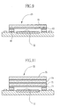
- Fig.7 is a cross sectional view of the solid state imaging device provided with an infrared cut filter layer and an optical low pass filter layer;
- Fig.8 is a cross sectional view illustrating a state where the infrared cut filter layer and the optical low pass filter layer are formed on the glass substrate by film deposition process;
- Fig.9 is a cross sectional view of the solid state imaging device in which an anti-reflection layer is formed by film deposition;
- Figs.10A to 10D are cross sectional views of the solid state imaging device illustrating procedure for forming the anti-reflection layer on the glass substrate;
- Fig.11 is a cross sectional view of the solid state imaging device provided with the anti-reflection layer, the infrared cut filter layer, and the optical low pass filter layer; and
- Fig.12 is a cross sectional view of a conventional camera module.
-
- Referring now to Fig.1, a
camera module 2 comprises a solidstate imaging device 3, a mounting board 4 to the solidstate imaging device 3, and anoptical unit 6 attached to the mounting board 4. Theoptical unit 6 has a takinglens 5 placed above the solidstate imaging device 3. - As shown in Fig.2 and Fig.3, the solid
state imaging device 3 is composed of animaging chip 8, aspacer 11, acover glass 12, and an optical filter layer formed on thecover glass 12. The optical filter layer includes at least an infraredcut filter layer 13 and an optical lowpass filter layer 14. - The
imaging chip 8 is constituted of asemiconductor substrate 10 and amicrolens array 9. Thesemiconductor substrate 10 is a chip diced off a silicon wafer, and animaging section 10a is formed thereon. Theimaging section 10a, as is commonly known, includes plural pixels arranged in a matrix, each of which pixels has a photoelectric conversion function and an electric charge accumulation function. The embodiment uses a CCD type imaging section which is composed of photodiodes and charge-coupled devices (CCD), however, a MOS type imaging section composed of photodiodes and MOS switches can also be used. - A mosaic filter is attached on the
imaging section 10a so that one of a red section, a green section, or a blue section of the mosaic filter is located immediately above its corresponding pixel. In addition, themicrolens array 9 is attached on the mosaic filter such that individual microlens agrees in position with each of the pixels. - The
spacer 11 has a square shape with anopening 17 in the middle, and is attached to an upper surface of thesemiconductor substrate 10 so as to enclose theimaging section 10a. Thespacer 11 is made from inorganic material such as a silicon or the like. Creating a gap between themicrolens array 9 and the cover glass (i.e. transparent cover) 12, thespacer 11 prevents the physical contact ofmicrolens array 9 with thecover glass 12. - The
cover glass 12 is attached to the upper surface of thespacer 11 to cover theopening 17. Thecover glass 12 is also made of a low alpha-ray emission glass, protecting each pixel of theimaging section 10a from being destroyed by an alpha-ray. - Outside the
spacer 11 on thesemiconductor substrate 10, a plurality ofouter connection terminals 20 are provided. Theouter connection terminals 20 are linked to theimaging section 10a through wiring on the surface of thesemiconductor substrate 10. Theouter connection terminals 20 are connected by wire bonding to the mounting board 4. - The infrared
cut filter layer 13 and the optical lowpass filter layer 14 improve quality of the images captured with the solidstate imaging device 3. The infraredcut filter layer 13 blocks the infrared ray within a particular wavelength range, eliminating ghost images and fog by the infrared light. The optical lowpass filter layer 14 blocks high frequency components in the spatial frequency, eliminating false color and moire effects. Because the infraredcut filter layer 13 and the optical lowpass filter layer 14 are bonded on thecover glass 12, theoptical unit 6 need not have the attachment space dedicated for them, and thecamera module 2 can thereby be downsized. Further, an anti-reflection filter layer may also be provided on the lower or upper surface of thecover glass 12 to prevent the incident light reflecting diffusely inside the solidstate imaging device 3. - The mounting board 4 is a rigid board, made of a glass epoxy board or a ceramic board, and is attached to both the solid
state imaging device 3 and theoptical unit 6. The mounting board 4 is provided with a drive circuit for the solidstate imaging device 3. Theoptical unit 6 comprises the takinglens 5 and alens holder 23. Thelens holder 23 includes aboxy base portion 23a to be attached to the mounting board 4 to cover the solidstate imaging device 3 and acylindrical lens barrel 23b to hold the takinglens 5. - A manufacturing process for the solid
state imaging device 3 is hereinafter described with reference to the flow chart of Fig. 4. In the first process, the optical filter layer is formed on aglass substrate 26, which is the base material of thecover glass 12. As shown in Fig.5A and Fig. 6, the optical filter layer is formed by bonding an infraredcut filter substrate 27 and an optical lowpass filter substrate 28 to theglass substrate 26 with anadhesive agent 29. The infraredcut filter substrate 27 and the optical lowpass filter substrate 28 are about the same size as theglass substrate 26. - The
adhesive agent 29 may be a ultraviolet adhesive, which turns into transparency after hardening. Theadhesive agent 29 is spread, with uniform thickness, on the entire surface of theglass substrate 26. In order to prevent air from incoming between the substrates, theglass substrate 26 is attached to the infraredcut filter substrate 27 under, for example, the vacuum environment. After attachment, one of theglass substrate 26 and the infraredcut filter substrate 27 is sucked with vacuum while the other is pressed with air pressure so that they stick to each other firmly. Subsequent ultraviolet irradiation through theglass substrate 26 hardens theadhesive agent 29, hence theglass substrate 26 and the infraredcut filter substrate 27 are put together tightly. The same attachment procedure as above applies to the optical lowpass filter substrate 28 onto the infraredcut filter substrate 27, and its detailed explanation is omitted. - As shown in Fig.5B illustrating the second process, a plurality of the
spacers 11 are formed on the lower surface of theglass substrate 26. Thespacer 11 is formed under the following procedure. Firstly, a silicon wafer for the spacer is attached on the lower surface of theglass substrate 26 with an adhesive agent. Secondly, a resist mask in the shape of thespacer 11 is formed on the silicon wafer by photolithography. Lastly, the portions without the resist mask are removed by plasma etching to form pluralities of thespacers 11 on theglass substrate 26. After the etching, the remaining resist mask on the silicon wafer is removed by ashing or the like. - Fig.5C and Fig. 6 show the third process, in which the
glass substrate 26 and asemiconductor wafer 32 are attached together with an adhesive agent. Formed in thesemiconductor wafer 32 are a plurality of theimaging sections 10a, on each of which themicrolens arrays 9 are attached. In this process, an alignment and bonding apparatus will be used. The alignment and bonding apparatus performs face to face alignment of theglass substrate 26 and thesemiconductor wafer 32, with reference to theirrespective orientation flats glass substrate 26 and thesemiconductor wafer 32 are attached together with the adhesive agent to form a substrate assembly. Upon this attachment, each of themicrolens arrays 9 is sealed by thespacer 11 and theglass substrate 26 on thesemiconductor wafer 32, protected from dust in the subsequent processes. - Fig.5D shows the fourth process, in which the
glass substrate 26, the infraredcut filter substrate 27 and the optical lowpass filter substrate 28 both attached to theglass substrate 26, and thesemiconductor wafer 32 are diced all together. In this process, the substrate assembly is placed on a dicing machine with a dicing tape adhering to theglass substrate 26. Pouring cooling water onto the substrate assembly, the dicing machine cuts off theglass substrate 26, the infraredcut filter substrate 27, the optical lowpass filter substrate 28, and thesemiconductor wafer 32 along each solidstate imaging device 3 with using, for example, a metal resin grinding wheel which is made from diamond abrasive grains bonded with a resin. Besides, it is also possible to dice theglass substrate 26 firstly, and then dice thesubstrate wafer 32. - When an eight-inch wafer is used, as many as two thousand solid
state imaging devices 3 are obtained all at once. Individually attaching the infraredcut filter layer 13 and the optical lowpass filter layer 14 to each of these two thousand solidstate imaging devices 3 may require considerable manufacturing costs and process steps. In this embodiment, however, the infraredcut filter substrate 27 and the optical lowpass filter substrate 28 are attached to theglass substrate 26 before theglass substrate 26 and thesemiconductor wafer 32 are diced together. This method only necessitates a single attaching process of the optical filter, and the manufacturing cost and the process steps are therefore reduced significantly. - The completed solid
state imaging device 3 undergoes functional tests, and is attached to the mounting board 4 together with theoptical unit 6 to compose thecamera module 2. Thecamera module 2 is incorporated in the portable electronic apparatuses such as cellular phones or the like. With the infraredcut filter layer 13 and the optical lowpass filter layer 14 formed on thecover glass 12 of the solid state and the optical low passfilter imaging device 3, thecamera module 2 of this embodiment is able to downsize theoptical unit 6 and, in fact, contributes to further downsizing of the portable electronic apparatuses which incorporate thecamera module 2. - Although the optical filter layer is formed by attaching the sheet-like or plate-like infrared
cut filter substrate 27 and optical lowpass filter substrate 28 to theglass substrate 26 in the above embodiment, it is also possible to deposit films of an infraredcut filter layer 35 and an optical lowpass filter layer 36 on acover glass 35, as a solidstate imaging device 34 shown in Fig.7. - In Fig.8, the optical filter layers are formed on a
glass substrate 38, which is the base material of thecover glass 35, by means of a CVD (chemical vapor deposition) machine, a vacuum vapor deposition machine or the like. As with the first embodiment described above, the processes of forming the spacers, attaching theglass substrate 35 to the semiconductor wafer, and dicing will follow to manufacture pluralities of the solidstate imaging devices 34 all at once. - Even in this embodiment, only a single deposition process is required for forming the optical filter layers on pluralities of the solid
state imaging devices 34, and thus the manufacturing cost and the process steps are much reduced than in the case where every solid state imaging devices undergo the deposition process. - In any of the foregoing embodiments, the optical filter layer is formed on the glass substrate before the glass substrate is attached to the semiconductor wafer. The glass substrate may, however, be attached to the semiconductor wafer before the optical filter layer is formed on the glass substrate by attaching or depositing films.
- In addition, a solid
state imaging device 60 shown in Fig.9 is provided with ananti-reflection filter layer 63 on the confronting surface of thecover glass 61 with amicrolens array 62 in order to prevent the incident light reflecting diffusely inside the solidstate imaging device 60. - To manufacture the solid
state imaging device 60, as shown in Fig.10A, theanti-reflection filter layer 63 is formed on a surface of aglass substrate 65, which is the base material of thecover glass 61, by such a film deposition method as the CVD or the vacuum vapor deposition. And a plurality ofspacers 67 are formed on theanti-reflection filter layer 63 as shown in Fig.10B. Then, as shown in Fig.10C, theglass substrate 65 is attached to asemiconductor wafer 68. Meanwhile, thesemiconductor wafer 68 has the same configuration as thesemiconductor wafer 32 shown in Fig.5C, and its detailed explanation will be omitted. Finally, as shown in Fig.10D, theglass substrate 65 and thesemiconductor wafer 68 are diced along each of themicrolens arrays 62. This method provides the solidstate imaging device 60 with theanti-reflection filter layer 63 on the lower surface, namely a facing surface to themicrolens array 62, of thecover glass 61. The anti-reflection filter layer can also be formed by attaching an anti-reflection filter plate or sheet to the glass substrate. - In a solid
state imaging device 70 shown in Fig.11, ananti-reflection filter layer 73 is formed on the lower surface of acover glass 71 by the film deposition process. On the upper surface of thecover glass 71, an infraredcut filter layer 74 and an optical lowpass filter layer 75 are formed either by attaching or depositing. When a plurality of optical filter layers are formed in a solid state imaging device, in addition, some filter layers may be formed by attaching and the others may be formed by depositing. - As described so far, the present invention is not to be limited to the above embodiments, and all matter contained herein is illustrative and does not limit the scope of the present invention. Thus, obvious modifications may be made within the spirit and scope of the appended claims.
Claims (24)
- A solid state imaging device (3, 34, 60, 70), formed by attaching a transparent substrate (26) onto a semiconductor wafer (32) having a plurality of imaging sections while keeping a predetermined gap created with a spacer (11, 67) surrounding each of said imaging sections and then cutting said transparent substrate (26) and said semiconductor wafer (32) along each of said imaging sections, comprising:an optical filter layer (13, 14, 36, 37, 63, 73, 74, 75) formed on a surface of said transparent substrate (26), being cut together with said transparent substrate (26).
- A solid state imaging device as claimed in claim 1, wherein said optical filter layer (13, 14, 36, 37, 63, 73, 74, 75) is an optical filter plate or sheet attached on said transparent substrate (26).
- A solid state imaging device as claimed in claim 2, wherein said optical filter layer (13, 14, 36, 37, 63, 73, 74, 75) is formed on an upper surface of said transparent substrate (26).
- A solid state imaging device as claimed in claim 2, wherein said optical filter layer is an infrared cut filter (13, 36, 74) .
- A solid state imaging device as claimed in claim 2, wherein said optical filter layer is an optical low pass filter (14, 37, 75).
- A solid state imaging device as claimed in claim 2, wherein said optical filter layer is a stacked layer of an optical low pass filter (14, 37, 75) and an infrared cut filter (13, 36, 74).
- A solid state imaging device as claimed in claim 1, wherein said optical filter layer (13, 14, 36, 37, 63, 73, 74, 75) is an optical filter film deposited on said surface of said transparent substrate (26).
- A solid state imaging device as claimed in claim 7, wherein said optical filter layer (13, 14, 36, 37, 63, 73, 74, 75) is formed on an upper surface of said transparent substrate (26).
- A solid state imaging device as claimed in claim 7, wherein said optical filter layer (13, 14, 36, 37, 63, 73, 74, 75) is formed on a lower surface of said transparent substrate.
- A solid state imaging device as claimed in claim 7, wherein said optical filter layer is an infrared cut filter (13, 36, 74).
- A solid state imaging device as claimed in claim 7, wherein said optical filter layer is an optical low pass filter (14, 37, 75).
- A solid state imaging device as claimed in claim 7, wherein said optical filter layer is a stacked layer of an optical low pass filter (14, 37, 75) and an infrared cut filter (13, 36, 74).
- A solid state imaging device as claimed in claim 7, wherein said optical filter layer is an anti-reflection filter (63, 73).
- A solid state imaging device as claimed in claim 7, wherein said optical filter layer is a stacked layer of an optical low pass filter (14, 37, 75), an infrared cut filter (13, 36, 74), and an anti-reflection filter (63, 73).
- A manufacturing method for a solid state imaging device (3, 34, 60, 70) comprising the steps of:(A) forming an optical filter layer (13, 14, 36, 37, 63, 73, 74, 75) on a surface of a transparent substrate (26);(B) attaching said transparent substrate (26) to a semiconductor wafer (32) having a plurality of imaging sections while keeping a predetermined gap; and(C) cutting said transparent substrate (26) and said semiconductor wafer (32) along each of said imaging sections.
- A manufacturing method as claimed in claim 15, wherein said step (A) is to attach an optical filter plate or sheet on said transparent substrate (26).
- A manufacturing method as claimed in claim 15, wherein said step (A) is to deposit an optical filter film on said surface of said transparent substrate (26).
- A manufacturing method as claimed in claim 16, wherein said step (A) is to form said optical filter layer on an upper surface of said transparent substrate (26).
- A manufacturing method as claimed in claim 17, wherein said step (A) is to form said optical filter layer on an upper surface of said transparent substrate (26).
- A manufacturing method as claimed in claim 17, wherein said step (A) is to form said optical filter layer on a lower surface of said transparent substrate (26).
- A manufacturing method for a solid state imaging device (3, 34, 60, 70) comprising the steps of:(A) attaching a transparent substrate (26) to a semiconductor wafer (32) having a plurality of imaging sections while keeping a predetermined gap;(B) forming an optical filter layer (13, 14, 36, 37, 63, 73, 74, 75) on a surface of said transparent substrate (26); and(C) cutting said transparent substrate (26) and said semiconductor wafer (32) along each of said imaging sections.
- A manufacturing method as claimed in claim 21, wherein said step (B) is to attach an optical filter plate or sheet on an upper surface of said transparent substrate (26).
- A manufacturing method as claimed in claim 21, wherein said step (B) is to deposit an optical filter film on an upper surface of said transparent substrate (26).
- A camera module (2) comprising:a circuit board (4);an optical unit (6) attached on said circuit board (4), holding a taking lens (5);an imaging device (3, 34, 60, 70) attached to said circuit board (4) inside said optical unit (6), said imaging device (3, 34, 60, 70) being formed by attaching a transparent substrate (26) onto a semiconductor wafer (32) having a plurality of imaging sections while keeping a predetermined gap and then dicing said semiconductor wafer (32) and said transparent substrate (26) along each of said imaging sections, said imaging device (3, 34, 60, 70) comprising:(a) a semiconductor substrate (10) diced off from said semiconductor wafer (32), having said image section;(b) a transparent cover (12, 35, 61, 71) diced off from said transparent substrate (26), for packaging said imaging section;(c) an optical filter layer (13, 14, 36, 37, 63, 73, 74, 75) formed on said transparent cover (12, 35, 61, 71), said optical filter layer (13, 14, 36, 37, 63, 73, 74, 75) being formed on said transparent substrate (26) and diced together with said transparent substrate (26).
Priority Applications (1)
| Application Number | Priority Date | Filing Date | Title |
|---|---|---|---|
| EP10009362A EP2253982A1 (en) | 2004-06-15 | 2005-06-14 | Solid-state imaging device and manufacturing method thereof |
Applications Claiming Priority (4)
| Application Number | Priority Date | Filing Date | Title |
|---|---|---|---|
| JP2004177419 | 2004-06-15 | ||
| JP2004177419 | 2004-06-15 | ||
| JP2004304768A JP2006032886A (en) | 2004-06-15 | 2004-10-19 | Solid-state imaging device, manufacturing method thereof, and camera module |
| JP2004304768 | 2004-10-19 |
Publications (2)
| Publication Number | Publication Date |
|---|---|
| EP1607782A2 true EP1607782A2 (en) | 2005-12-21 |
| EP1607782A3 EP1607782A3 (en) | 2006-12-20 |
Family
ID=34977065
Family Applications (2)
| Application Number | Title | Priority Date | Filing Date |
|---|---|---|---|
| EP10009362A Withdrawn EP2253982A1 (en) | 2004-06-15 | 2005-06-14 | Solid-state imaging device and manufacturing method thereof |
| EP05253677A Withdrawn EP1607782A3 (en) | 2004-06-15 | 2005-06-14 | Solid-state imaging device and manufacturing method thereof, and camera module |
Family Applications Before (1)
| Application Number | Title | Priority Date | Filing Date |
|---|---|---|---|
| EP10009362A Withdrawn EP2253982A1 (en) | 2004-06-15 | 2005-06-14 | Solid-state imaging device and manufacturing method thereof |
Country Status (4)
| Country | Link |
|---|---|
| US (2) | US20050275746A1 (en) |
| EP (2) | EP2253982A1 (en) |
| JP (1) | JP2006032886A (en) |
| KR (1) | KR100691711B1 (en) |
Cited By (5)
| Publication number | Priority date | Publication date | Assignee | Title |
|---|---|---|---|---|
| DE102007057172A1 (en) * | 2007-11-26 | 2009-05-28 | Silicon Micro Sensors Gmbh | Stereo camera for environmental detection |
| EP2069851A4 (en) * | 2006-09-14 | 2010-02-24 | Tessera Tech Hungary Kft | IMAGING SYSTEM WITH ASSOUPLY ASSEMBLED TOLERANCES AND ASSOCIATED METHODS |
| US9350976B2 (en) | 2007-11-26 | 2016-05-24 | First Sensor Mobility Gmbh | Imaging unit of a camera for recording the surroundings with optics uncoupled from a circuit board |
| CN107843966A (en) * | 2016-09-18 | 2018-03-27 | 中芯国际集成电路制造(上海)有限公司 | For assembling the method and system of microlens array component |
| EP2718630B1 (en) * | 2011-06-06 | 2022-07-06 | Schott Ag | Indication apparatus |
Families Citing this family (37)
| Publication number | Priority date | Publication date | Assignee | Title |
|---|---|---|---|---|
| JP2006100763A (en) * | 2004-09-06 | 2006-04-13 | Fuji Photo Film Co Ltd | Solid-state imaging device manufacturing method and joining device |
| WO2006109638A1 (en) * | 2005-04-08 | 2006-10-19 | Konica Minolta Opto, Inc. | Solid-state image pickup element and method for manufacturing same |
| US8093672B2 (en) * | 2005-10-28 | 2012-01-10 | Panasonic Corporation | Solid-state imaging device |
| JP5427337B2 (en) * | 2005-12-21 | 2014-02-26 | セミコンダクター・コンポーネンツ・インダストリーズ・リミテッド・ライアビリティ・カンパニー | Semiconductor device, method for manufacturing the same, and camera module |
| JP2007208045A (en) * | 2006-02-02 | 2007-08-16 | Sony Corp | Imaging device, camera module, electronic device, and manufacturing method of imaging device |
| KR100747611B1 (en) * | 2006-03-08 | 2007-08-08 | 삼성전자주식회사 | Microelement Package and Manufacturing Method Thereof |
| CN101047783A (en) * | 2006-03-31 | 2007-10-03 | 鸿富锦精密工业(深圳)有限公司 | Micro-camera device |
| CN101114039A (en) * | 2006-07-28 | 2008-01-30 | 鸿富锦精密工业(深圳)有限公司 | lens module |
| JP2008066702A (en) | 2006-08-10 | 2008-03-21 | Matsushita Electric Ind Co Ltd | Solid-state image sensor and camera |
| CN101261347A (en) * | 2007-03-09 | 2008-09-10 | 鸿富锦精密工业(深圳)有限公司 | Camera module and manufacturing method thereof |
| KR100862486B1 (en) * | 2007-05-31 | 2008-10-08 | 삼성전기주식회사 | Camera module package |
| KR100906841B1 (en) * | 2007-10-01 | 2009-07-08 | 엘지이노텍 주식회사 | Camera module and its manufacturing method |
| CN101419323A (en) * | 2007-10-22 | 2009-04-29 | 鸿富锦精密工业(深圳)有限公司 | Mini camera module and method for producing the same |
| CN101465344B (en) * | 2007-12-18 | 2011-02-02 | 鸿富锦精密工业(深圳)有限公司 | Encapsulation structure of image die set |
| EP2075840B1 (en) * | 2007-12-28 | 2014-08-27 | Semiconductor Energy Laboratory Co., Ltd. | Method for dicing a wafer with semiconductor elements formed thereon and corresponding device |
| JP5317712B2 (en) * | 2008-01-22 | 2013-10-16 | 株式会社半導体エネルギー研究所 | Semiconductor device and manufacturing method of semiconductor device |
| JP5376961B2 (en) * | 2008-02-01 | 2013-12-25 | 株式会社半導体エネルギー研究所 | Semiconductor device |
| JP5175620B2 (en) * | 2008-05-29 | 2013-04-03 | シャープ株式会社 | Electronic element wafer module and manufacturing method thereof, electronic element module, and electronic information device |
| JP5299188B2 (en) * | 2009-09-16 | 2013-09-25 | 富士通株式会社 | Imaging device, electronic device including the same, and manufacturing method of imaging device |
| JP5635378B2 (en) * | 2010-11-30 | 2014-12-03 | 日東電工株式会社 | Semiconductor wafer transfer method and semiconductor wafer transfer apparatus |
| TW201349470A (en) * | 2012-05-16 | 2013-12-01 | 海華科技股份有限公司 | Image sensing module for reducing overall thickness |
| JP6281214B2 (en) * | 2013-06-06 | 2018-02-21 | 株式会社リコー | Image pickup device package and image pickup apparatus |
| JP2015032653A (en) | 2013-08-01 | 2015-02-16 | 株式会社東芝 | Solid state imaging apparatus |
| TWI512961B (en) * | 2013-08-16 | 2015-12-11 | Azurewave Technologies Inc | Image sensing module for reducing overall thickness and manufacturing method thereof |
| US9386203B2 (en) * | 2013-10-28 | 2016-07-05 | Omnivision Technologies, Inc. | Compact spacer in multi-lens array module |
| JP6300029B2 (en) | 2014-01-27 | 2018-03-28 | ソニー株式会社 | Image sensor, manufacturing apparatus, and manufacturing method |
| KR101856554B1 (en) * | 2014-02-20 | 2018-05-10 | 후지필름 가부시키가이샤 | Photosensitive resin composition, cured object and production method therefor, resin pattern production method, cured film, liquid crystal display device, organic el display device, infrared cutoff filter, and solid imaging device |
| JP6333947B2 (en) * | 2014-02-20 | 2018-05-30 | 富士フイルム株式会社 | Photosensitive resin composition, cured product and manufacturing method thereof, resin pattern manufacturing method, cured film, liquid crystal display device, organic EL display device, infrared cut filter, and solid-state imaging device |
| US10466501B2 (en) * | 2016-05-26 | 2019-11-05 | Ams Sensors Singapore Pte. Ltd. | Optoelectronic modules including an optical system tilted with respect to a focal plane |
| JP6791584B2 (en) * | 2017-02-01 | 2020-11-25 | 株式会社ディスコ | Processing method |
| JPWO2019026848A1 (en) | 2017-07-31 | 2020-08-13 | Jsr株式会社 | Photoelectric conversion device |
| JP7060018B2 (en) * | 2017-07-31 | 2022-04-26 | Jsr株式会社 | Photoelectric conversion element and adhesive |
| JP2019029525A (en) * | 2017-07-31 | 2019-02-21 | Jsr株式会社 | Ambient light sensor and composition for forming adhesive layer |
| JP2019050338A (en) * | 2017-09-12 | 2019-03-28 | ソニーセミコンダクタソリューションズ株式会社 | Imaging device, method of manufacturing imaging device, imaging device, and electronic apparatus |
| FR3078438B1 (en) * | 2018-02-27 | 2020-07-17 | Stmicroelectronics (Grenoble 2) Sas | PROCESS FOR MANUFACTURING A PLURALITY OF ELECTRONIC PACKAGES |
| CN111147628B (en) * | 2018-11-01 | 2024-01-19 | 广州立景创新科技有限公司 | Image capture component |
| WO2020236575A1 (en) * | 2019-05-17 | 2020-11-26 | Photon-X, Inc. | Spatial phase integrated wafer-level imaging |
Citations (5)
| Publication number | Priority date | Publication date | Assignee | Title |
|---|---|---|---|---|
| JP2002231921A (en) | 2001-02-06 | 2002-08-16 | Olympus Optical Co Ltd | Solid-state image pickup device and its manufacturing method |
| US20030007033A1 (en) * | 2001-07-04 | 2003-01-09 | Seiko Epson Corporation | System and methods for manufacturing a color filter using a scanning ink jet head |
| JP2003037293A (en) * | 2001-07-25 | 2003-02-07 | Nichia Chem Ind Ltd | Chip component type light emitting device and method of manufacturing the same |
| JP2004064272A (en) | 2002-07-26 | 2004-02-26 | West Electric Co Ltd | Camera module |
| US20040223072A1 (en) | 2003-05-08 | 2004-11-11 | Fuji Photo Film Co., Ltd. | Solid-state imaging device, camera module, and camera-module manufacturing method |
Family Cites Families (6)
| Publication number | Priority date | Publication date | Assignee | Title |
|---|---|---|---|---|
| JP2000216368A (en) * | 1999-01-25 | 2000-08-04 | Asahi Optical Co Ltd | Infrared cut filter mounting structure of imaging device |
| JP2001339055A (en) * | 2000-05-29 | 2001-12-07 | Asahi Optical Co Ltd | Cover member of solid-state imaging device and solid-state imaging device |
| US6635941B2 (en) * | 2001-03-21 | 2003-10-21 | Canon Kabushiki Kaisha | Structure of semiconductor device with improved reliability |
| JP2002373977A (en) * | 2001-06-14 | 2002-12-26 | Canon Inc | Solid-state imaging device |
| US7033664B2 (en) * | 2002-10-22 | 2006-04-25 | Tessera Technologies Hungary Kft | Methods for producing packaged integrated circuit devices and packaged integrated circuit devices produced thereby |
| US7329861B2 (en) * | 2003-10-14 | 2008-02-12 | Micron Technology, Inc. | Integrally packaged imaging module |
-
2004
- 2004-10-19 JP JP2004304768A patent/JP2006032886A/en active Pending
-
2005
- 2005-06-14 KR KR1020050050767A patent/KR100691711B1/en not_active Expired - Fee Related
- 2005-06-14 US US11/151,340 patent/US20050275746A1/en not_active Abandoned
- 2005-06-14 EP EP10009362A patent/EP2253982A1/en not_active Withdrawn
- 2005-06-14 EP EP05253677A patent/EP1607782A3/en not_active Withdrawn
-
2008
- 2008-08-28 US US12/200,444 patent/US20090002532A1/en not_active Abandoned
Patent Citations (5)
| Publication number | Priority date | Publication date | Assignee | Title |
|---|---|---|---|---|
| JP2002231921A (en) | 2001-02-06 | 2002-08-16 | Olympus Optical Co Ltd | Solid-state image pickup device and its manufacturing method |
| US20030007033A1 (en) * | 2001-07-04 | 2003-01-09 | Seiko Epson Corporation | System and methods for manufacturing a color filter using a scanning ink jet head |
| JP2003037293A (en) * | 2001-07-25 | 2003-02-07 | Nichia Chem Ind Ltd | Chip component type light emitting device and method of manufacturing the same |
| JP2004064272A (en) | 2002-07-26 | 2004-02-26 | West Electric Co Ltd | Camera module |
| US20040223072A1 (en) | 2003-05-08 | 2004-11-11 | Fuji Photo Film Co., Ltd. | Solid-state imaging device, camera module, and camera-module manufacturing method |
Cited By (9)
| Publication number | Priority date | Publication date | Assignee | Title |
|---|---|---|---|---|
| EP2069851A4 (en) * | 2006-09-14 | 2010-02-24 | Tessera Tech Hungary Kft | IMAGING SYSTEM WITH ASSOUPLY ASSEMBLED TOLERANCES AND ASSOCIATED METHODS |
| US8159602B2 (en) | 2006-09-14 | 2012-04-17 | DigitalOptics Corporation Europe Limited | Imaging system with relaxed assembly tolerances and associated methods |
| DE102007057172A1 (en) * | 2007-11-26 | 2009-05-28 | Silicon Micro Sensors Gmbh | Stereo camera for environmental detection |
| DE102007057172B4 (en) * | 2007-11-26 | 2009-07-02 | Silicon Micro Sensors Gmbh | Stereo camera for environmental detection |
| US8488045B2 (en) | 2007-11-26 | 2013-07-16 | Silicon Micro Sensors Gmbh | Stereoscopic camera for recording the surroundings |
| US9350976B2 (en) | 2007-11-26 | 2016-05-24 | First Sensor Mobility Gmbh | Imaging unit of a camera for recording the surroundings with optics uncoupled from a circuit board |
| US10212320B2 (en) | 2007-11-26 | 2019-02-19 | First Sensor Mobility Gmbh | Imaging unit of a camera for recording the surroundings with optics uncoupled from a circuit board |
| EP2718630B1 (en) * | 2011-06-06 | 2022-07-06 | Schott Ag | Indication apparatus |
| CN107843966A (en) * | 2016-09-18 | 2018-03-27 | 中芯国际集成电路制造(上海)有限公司 | For assembling the method and system of microlens array component |
Also Published As
| Publication number | Publication date |
|---|---|
| KR20060049586A (en) | 2006-05-19 |
| JP2006032886A (en) | 2006-02-02 |
| US20050275746A1 (en) | 2005-12-15 |
| KR100691711B1 (en) | 2007-03-09 |
| EP1607782A3 (en) | 2006-12-20 |
| EP2253982A1 (en) | 2010-11-24 |
| US20090002532A1 (en) | 2009-01-01 |
Similar Documents
| Publication | Publication Date | Title |
|---|---|---|
| EP1607782A2 (en) | Solid-state imaging device and manufacturing method thereof, and camera module | |
| TWI394269B (en) | Electronic component wafer module, electronic component wafer module manufacturing method, electronic component module and electronic information device | |
| US7723741B2 (en) | Spacers for packaged microelectronic imagers and methods of making and using spacers for wafer-level packaging of imagers | |
| US7511262B2 (en) | Optical device and assembly for use with imaging dies, and wafer-label imager assembly | |
| US8456560B2 (en) | Wafer level camera module and method of manufacture | |
| US7923798B2 (en) | Optical device and method for fabricating the same, camera module using optical device, and electronic equipment mounting camera module | |
| US7189954B2 (en) | Microelectronic imagers with optical devices and methods of manufacturing such microelectronic imagers | |
| US7547877B2 (en) | Microelectronic imagers with integrated optical devices and methods for manufacturing such microelectronic imagers | |
| US20100044815A1 (en) | Cmos image sensor package and camera module using same | |
| US7901973B2 (en) | Solid state imaging device and manufacturing method thereof | |
| TWI467747B (en) | Solid-state imaging device and method of manufacturing same | |
| CN1985379A (en) | Covers for microelectronic imagers and methods for wafer-level packaging of microelectronic imagers | |
| JP4672301B2 (en) | Solid-state imaging device and method for manufacturing solid-state imaging device | |
| JP2009290033A (en) | Electronic device wafer module and its production process, electronic device module, electronic information equipment | |
| WO2007052796A1 (en) | Module for optical device, method of manufacturing module for optical device and structure for device | |
| KR100809682B1 (en) | Method for manufacturing optical device with transparent cover and method for manufacturing optical device module using same | |
| CN100459140C (en) | Solid-state imaging device, manufacturing method thereof, and camera module | |
| US20080203508A1 (en) | Image sensing device having protection pattern on the microlens, camera module, and method of forming the same | |
| JP2006100859A (en) | Solid state imaging device and manufacturing method of the same | |
| JP2006049371A (en) | Packing structure of solid-state imaging device |
Legal Events
| Date | Code | Title | Description |
|---|---|---|---|
| PUAI | Public reference made under article 153(3) epc to a published international application that has entered the european phase |
Free format text: ORIGINAL CODE: 0009012 |
|
| AK | Designated contracting states |
Kind code of ref document: A2 Designated state(s): AT BE BG CH CY CZ DE DK EE ES FI FR GB GR HU IE IS IT LI LT LU MC NL PL PT RO SE SI SK TR |
|
| AX | Request for extension of the european patent |
Extension state: AL BA HR LV MK YU |
|
| PUAL | Search report despatched |
Free format text: ORIGINAL CODE: 0009013 |
|
| AK | Designated contracting states |
Kind code of ref document: A3 Designated state(s): AT BE BG CH CY CZ DE DK EE ES FI FR GB GR HU IE IS IT LI LT LU MC NL PL PT RO SE SI SK TR |
|
| AX | Request for extension of the european patent |
Extension state: AL BA HR LV MK YU |
|
| RIC1 | Information provided on ipc code assigned before grant |
Ipc: H01L 31/0216 20060101ALI20061116BHEP Ipc: H01L 27/146 20060101ALI20061116BHEP Ipc: H04N 5/225 20060101ALI20061116BHEP Ipc: G02B 13/00 20060101ALI20061116BHEP Ipc: G02B 7/02 20060101ALI20061116BHEP Ipc: G02B 7/00 20060101AFI20050927BHEP |
|
| RAP1 | Party data changed (applicant data changed or rights of an application transferred) |
Owner name: FUJIFILM CORPORATION |
|
| 17P | Request for examination filed |
Effective date: 20070618 |
|
| 17Q | First examination report despatched |
Effective date: 20070719 |
|
| AKX | Designation fees paid |
Designated state(s): DE FR GB |
|
| STAA | Information on the status of an ep patent application or granted ep patent |
Free format text: STATUS: THE APPLICATION IS DEEMED TO BE WITHDRAWN |
|
| 18D | Application deemed to be withdrawn |
Effective date: 20101202 |