EP1607457A2 - Elektrisch anisotrop leitfähiger Schmelzkleber zur Implantierung von elektrischen Modulen in einen Kartenkörper - Google Patents
Elektrisch anisotrop leitfähiger Schmelzkleber zur Implantierung von elektrischen Modulen in einen Kartenkörper Download PDFInfo
- Publication number
- EP1607457A2 EP1607457A2 EP05104783A EP05104783A EP1607457A2 EP 1607457 A2 EP1607457 A2 EP 1607457A2 EP 05104783 A EP05104783 A EP 05104783A EP 05104783 A EP05104783 A EP 05104783A EP 1607457 A2 EP1607457 A2 EP 1607457A2
- Authority
- EP
- European Patent Office
- Prior art keywords
- adhesive
- conductive particles
- particles
- adhesive system
- bonding
- Prior art date
- Legal status (The legal status is an assumption and is not a legal conclusion. Google has not performed a legal analysis and makes no representation as to the accuracy of the status listed.)
- Withdrawn
Links
Images
Classifications
-
- C—CHEMISTRY; METALLURGY
- C09—DYES; PAINTS; POLISHES; NATURAL RESINS; ADHESIVES; COMPOSITIONS NOT OTHERWISE PROVIDED FOR; APPLICATIONS OF MATERIALS NOT OTHERWISE PROVIDED FOR
- C09J—ADHESIVES; NON-MECHANICAL ASPECTS OF ADHESIVE PROCESSES IN GENERAL; ADHESIVE PROCESSES NOT PROVIDED FOR ELSEWHERE; USE OF MATERIALS AS ADHESIVES
- C09J7/00—Adhesives in the form of films or foils
- C09J7/30—Adhesives in the form of films or foils characterised by the adhesive composition
- C09J7/35—Heat-activated
-
- G—PHYSICS
- G06—COMPUTING OR CALCULATING; COUNTING
- G06K—GRAPHICAL DATA READING; PRESENTATION OF DATA; RECORD CARRIERS; HANDLING RECORD CARRIERS
- G06K19/00—Record carriers for use with machines and with at least a part designed to carry digital markings
- G06K19/06—Record carriers for use with machines and with at least a part designed to carry digital markings characterised by the kind of the digital marking, e.g. shape, nature, code
- G06K19/067—Record carriers with conductive marks, printed circuits or semiconductor circuit elements, e.g. credit or identity cards also with resonating or responding marks without active components
- G06K19/07—Record carriers with conductive marks, printed circuits or semiconductor circuit elements, e.g. credit or identity cards also with resonating or responding marks without active components with integrated circuit chips
- G06K19/077—Constructional details, e.g. mounting of circuits in the carrier
- G06K19/07745—Mounting details of integrated circuit chips
-
- C—CHEMISTRY; METALLURGY
- C09—DYES; PAINTS; POLISHES; NATURAL RESINS; ADHESIVES; COMPOSITIONS NOT OTHERWISE PROVIDED FOR; APPLICATIONS OF MATERIALS NOT OTHERWISE PROVIDED FOR
- C09J—ADHESIVES; NON-MECHANICAL ASPECTS OF ADHESIVE PROCESSES IN GENERAL; ADHESIVE PROCESSES NOT PROVIDED FOR ELSEWHERE; USE OF MATERIALS AS ADHESIVES
- C09J11/00—Features of adhesives not provided for in group C09J9/00, e.g. additives
- C09J11/02—Non-macromolecular additives
- C09J11/04—Non-macromolecular additives inorganic
-
- C—CHEMISTRY; METALLURGY
- C09—DYES; PAINTS; POLISHES; NATURAL RESINS; ADHESIVES; COMPOSITIONS NOT OTHERWISE PROVIDED FOR; APPLICATIONS OF MATERIALS NOT OTHERWISE PROVIDED FOR
- C09J—ADHESIVES; NON-MECHANICAL ASPECTS OF ADHESIVE PROCESSES IN GENERAL; ADHESIVE PROCESSES NOT PROVIDED FOR ELSEWHERE; USE OF MATERIALS AS ADHESIVES
- C09J5/00—Adhesive processes in general; Adhesive processes not provided for elsewhere, e.g. relating to primers
- C09J5/06—Adhesive processes in general; Adhesive processes not provided for elsewhere, e.g. relating to primers involving heating of the applied adhesive
-
- C—CHEMISTRY; METALLURGY
- C09—DYES; PAINTS; POLISHES; NATURAL RESINS; ADHESIVES; COMPOSITIONS NOT OTHERWISE PROVIDED FOR; APPLICATIONS OF MATERIALS NOT OTHERWISE PROVIDED FOR
- C09J—ADHESIVES; NON-MECHANICAL ASPECTS OF ADHESIVE PROCESSES IN GENERAL; ADHESIVE PROCESSES NOT PROVIDED FOR ELSEWHERE; USE OF MATERIALS AS ADHESIVES
- C09J7/00—Adhesives in the form of films or foils
- C09J7/10—Adhesives in the form of films or foils without carriers
-
- C—CHEMISTRY; METALLURGY
- C09—DYES; PAINTS; POLISHES; NATURAL RESINS; ADHESIVES; COMPOSITIONS NOT OTHERWISE PROVIDED FOR; APPLICATIONS OF MATERIALS NOT OTHERWISE PROVIDED FOR
- C09J—ADHESIVES; NON-MECHANICAL ASPECTS OF ADHESIVE PROCESSES IN GENERAL; ADHESIVE PROCESSES NOT PROVIDED FOR ELSEWHERE; USE OF MATERIALS AS ADHESIVES
- C09J9/00—Adhesives characterised by their physical nature or the effects produced, e.g. glue sticks
- C09J9/02—Electrically-conducting adhesives
-
- H—ELECTRICITY
- H05—ELECTRIC TECHNIQUES NOT OTHERWISE PROVIDED FOR
- H05K—PRINTED CIRCUITS; CASINGS OR CONSTRUCTIONAL DETAILS OF ELECTRIC APPARATUS; MANUFACTURE OF ASSEMBLAGES OF ELECTRICAL COMPONENTS
- H05K3/00—Apparatus or processes for manufacturing printed circuits
- H05K3/30—Assembling printed circuits with electric components, e.g. with resistors
- H05K3/32—Assembling printed circuits with electric components, e.g. with resistors electrically connecting electric components or wires to printed circuits
- H05K3/321—Assembling printed circuits with electric components, e.g. with resistors electrically connecting electric components or wires to printed circuits by conductive adhesives
- H05K3/323—Assembling printed circuits with electric components, e.g. with resistors electrically connecting electric components or wires to printed circuits by conductive adhesives by applying an anisotropic conductive adhesive layer over an array of pads
-
- C—CHEMISTRY; METALLURGY
- C09—DYES; PAINTS; POLISHES; NATURAL RESINS; ADHESIVES; COMPOSITIONS NOT OTHERWISE PROVIDED FOR; APPLICATIONS OF MATERIALS NOT OTHERWISE PROVIDED FOR
- C09J—ADHESIVES; NON-MECHANICAL ASPECTS OF ADHESIVE PROCESSES IN GENERAL; ADHESIVE PROCESSES NOT PROVIDED FOR ELSEWHERE; USE OF MATERIALS AS ADHESIVES
- C09J2203/00—Applications of adhesives in processes or use of adhesives in the form of films or foils
- C09J2203/326—Applications of adhesives in processes or use of adhesives in the form of films or foils for bonding electronic components such as wafers, chips or semiconductors
-
- C—CHEMISTRY; METALLURGY
- C09—DYES; PAINTS; POLISHES; NATURAL RESINS; ADHESIVES; COMPOSITIONS NOT OTHERWISE PROVIDED FOR; APPLICATIONS OF MATERIALS NOT OTHERWISE PROVIDED FOR
- C09J—ADHESIVES; NON-MECHANICAL ASPECTS OF ADHESIVE PROCESSES IN GENERAL; ADHESIVE PROCESSES NOT PROVIDED FOR ELSEWHERE; USE OF MATERIALS AS ADHESIVES
- C09J2301/00—Additional features of adhesives in the form of films or foils
- C09J2301/30—Additional features of adhesives in the form of films or foils characterized by the chemical, physicochemical or physical properties of the adhesive or the carrier
- C09J2301/304—Additional features of adhesives in the form of films or foils characterized by the chemical, physicochemical or physical properties of the adhesive or the carrier the adhesive being heat-activatable, i.e. not tacky at temperatures inferior to 30°C
-
- C—CHEMISTRY; METALLURGY
- C09—DYES; PAINTS; POLISHES; NATURAL RESINS; ADHESIVES; COMPOSITIONS NOT OTHERWISE PROVIDED FOR; APPLICATIONS OF MATERIALS NOT OTHERWISE PROVIDED FOR
- C09J—ADHESIVES; NON-MECHANICAL ASPECTS OF ADHESIVE PROCESSES IN GENERAL; ADHESIVE PROCESSES NOT PROVIDED FOR ELSEWHERE; USE OF MATERIALS AS ADHESIVES
- C09J2301/00—Additional features of adhesives in the form of films or foils
- C09J2301/30—Additional features of adhesives in the form of films or foils characterized by the chemical, physicochemical or physical properties of the adhesive or the carrier
- C09J2301/314—Additional features of adhesives in the form of films or foils characterized by the chemical, physicochemical or physical properties of the adhesive or the carrier the adhesive layer and/or the carrier being conductive
-
- H—ELECTRICITY
- H05—ELECTRIC TECHNIQUES NOT OTHERWISE PROVIDED FOR
- H05K—PRINTED CIRCUITS; CASINGS OR CONSTRUCTIONAL DETAILS OF ELECTRIC APPARATUS; MANUFACTURE OF ASSEMBLAGES OF ELECTRICAL COMPONENTS
- H05K1/00—Printed circuits
- H05K1/18—Printed circuits structurally associated with non-printed electric components
- H05K1/182—Printed circuits structurally associated with non-printed electric components associated with components mounted in printed circuit boards [PCB], e.g. insert-mounted components [IMC]
- H05K1/183—Printed circuits structurally associated with non-printed electric components associated with components mounted in printed circuit boards [PCB], e.g. insert-mounted components [IMC] associated with components mounted in and supported by recessed areas of the PCBs
-
- H—ELECTRICITY
- H05—ELECTRIC TECHNIQUES NOT OTHERWISE PROVIDED FOR
- H05K—PRINTED CIRCUITS; CASINGS OR CONSTRUCTIONAL DETAILS OF ELECTRIC APPARATUS; MANUFACTURE OF ASSEMBLAGES OF ELECTRICAL COMPONENTS
- H05K2201/00—Indexing scheme relating to printed circuits covered by H05K1/00
- H05K2201/02—Fillers; Particles; Fibers; Reinforcement materials
- H05K2201/0203—Fillers and particles
- H05K2201/0263—Details about a collection of particles
- H05K2201/0266—Size distribution
-
- H—ELECTRICITY
- H05—ELECTRIC TECHNIQUES NOT OTHERWISE PROVIDED FOR
- H05K—PRINTED CIRCUITS; CASINGS OR CONSTRUCTIONAL DETAILS OF ELECTRIC APPARATUS; MANUFACTURE OF ASSEMBLAGES OF ELECTRICAL COMPONENTS
- H05K2201/00—Indexing scheme relating to printed circuits covered by H05K1/00
- H05K2201/10—Details of components or other objects attached to or integrated in a printed circuit board
- H05K2201/10613—Details of electrical connections of non-printed components, e.g. special leads
- H05K2201/10621—Components characterised by their electrical contacts
- H05K2201/10727—Leadless chip carrier [LCC], e.g. chip-modules for cards
-
- Y—GENERAL TAGGING OF NEW TECHNOLOGICAL DEVELOPMENTS; GENERAL TAGGING OF CROSS-SECTIONAL TECHNOLOGIES SPANNING OVER SEVERAL SECTIONS OF THE IPC; TECHNICAL SUBJECTS COVERED BY FORMER USPC CROSS-REFERENCE ART COLLECTIONS [XRACs] AND DIGESTS
- Y10—TECHNICAL SUBJECTS COVERED BY FORMER USPC
- Y10T—TECHNICAL SUBJECTS COVERED BY FORMER US CLASSIFICATION
- Y10T428/00—Stock material or miscellaneous articles
- Y10T428/25—Web or sheet containing structurally defined element or component and including a second component containing structurally defined particles
- Y10T428/256—Heavy metal or aluminum or compound thereof
-
- Y—GENERAL TAGGING OF NEW TECHNOLOGICAL DEVELOPMENTS; GENERAL TAGGING OF CROSS-SECTIONAL TECHNOLOGIES SPANNING OVER SEVERAL SECTIONS OF THE IPC; TECHNICAL SUBJECTS COVERED BY FORMER USPC CROSS-REFERENCE ART COLLECTIONS [XRACs] AND DIGESTS
- Y10—TECHNICAL SUBJECTS COVERED BY FORMER USPC
- Y10T—TECHNICAL SUBJECTS COVERED BY FORMER US CLASSIFICATION
- Y10T428/00—Stock material or miscellaneous articles
- Y10T428/26—Web or sheet containing structurally defined element or component, the element or component having a specified physical dimension
- Y10T428/261—In terms of molecular thickness or light wave length
Definitions
- the invention relates to an anisotropically electrically conductive hot melt adhesive for bonding of electrical modules in card bodies as well as for the permanent production of a electrical contact between the electrical module and antenna in the card body.
- Hot melt adhesives are clearly superior to liquid adhesives. Nevertheless, that is Selection of suitable connections here too very limited, as very high requirements be put to this joining technique.
- anisotropically conductive adhesives have been around for a long time known.
- the adhesive electrically conductive particles in one certain amount mixed.
- concentration you can avoid that a conductivity in the XY direction is formed.
- the electrical conductivity in the Z-direction is achieved in that the electrically conductive particles partially in Diameters are greater than the layer thickness of the adhesive. After compression arises thus the direct contact between the electrical contacts to be connected.
- No. 5,499,730 describes a process for producing anisotropically electrically conductive Adhesive tapes described.
- Adhesive tapes described.
- the corresponding particles in regular Spaced on the adhesive, otherwise in the processing of extrusion It is feared that the particles will be destroyed in the extrusion process.
- No. 6,426,021 describes an anisotropically conductive adhesive based on a reactive system and electrically conductive particles proposed for bonding of IC chips.
- reactive systems have the disadvantage that substances are released by reactions can be, which favor the corrosion of the electrically conductive particles or as a gaseous component build up a back pressure and thus the bond counteract.
- the glue should be at low temperatures do not embrittle, do not liquefy at high temperatures and a low Have a tendency to absorb water.
- the invention is based on the object in view of this prior art an anisotropically electrically conductive adhesive film for implanting electrical Specify modules in a card body that meets the above criteria.
- an anisotropically conductive adhesive film comprising at least one layer of an adhesive system based on at least one heat-activable adhesive, wherein the softening temperature of the adhesive system in the range of 65 ° C to 165 ° C and wherein the adhesive system electrically conductive particles are mixed, further wherein the particles have an average diameter of 25 to 100 microns, provided that the average diameter of the conductive particles is greater than the layer thickness of the adhesive system.
- the data of the softening temperature are based on the measuring method according to DIN 53460.
- Particularly advantageous according to the invention is an adhesive film in which the added conductive particles have a copper or nickel core. and / or at the conductive Particles have a gold or a silver sheath.
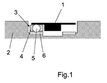
- the bonding of the electrical module with a card body is shown in Figure 1) shown schematically.
- 1 denotes the dual interface module
- 2 the card body
- 3 the adhesive film according to the invention, consisting of the adhesive 4 and the mixed electrically conductive particles 5, and 6 the antenna
- the inventive temperature-activatable Adhesive composition has in a preferred embodiment a Layer thickness between 20 and 95 microns, in a particularly preferred embodiment a layer thickness of 30 to 80 microns.
- the heat-activatable adhesive has a bond for bonding the electrical module good adhesion to epoxy materials, polyesters and polyimides and for bonding Card bodies have good adhesion to PC, ABS, PVC and PET.
- thermoplastic materials such. polyurethanes, Polyesters, polyamides, ethylene vinyl acetates, synthetic rubbers, e.g.
- styrene isoprene Di- and triblock copolymers SIS
- styrene-butadiene di- and triblock copolymers SBS
- Styrene-ethylene-butadiene di- and triblock copolymer SEBS
- polyvinyl acetate polyimides
- Polyethers copolyamides
- copolyesters polyolefins, e.g. Polyethylene, polypropylene, or poly (meth) crylate.
- the list is not exhaustive.
- the polymers have a softening range between 65 and 175 ° C.
- the preferred proportion of Resins is between 2 and 50 wt .-%, based on the thermoplastic.
- Adhesive resins to be added are the tackifier resins described in the literature used. Mention may be made of the pinene, indene and rosin resins, their disproportionated, hydrogenated, polymerized, esterified derivatives and salts, the aliphatic and aromatic hydrocarbon resins, terpene resins and terpene phenolic resins and C5, C9 and other hydrocarbon resins. Any combinations These and other resins can be used to control the properties of adjust the resulting adhesive as desired.
- thermoplastic compatible (soluble) resins In general, everyone can use with the appropriate thermoplastic compatible (soluble) resins, in particular reference is made to all aliphatic, aromatic, alkylaromatic hydrocarbon resins, Hydrocarbon resins based on pure monomers, hydrogenated hydrocarbon resins, functional hydrocarbon resins and natural resins. On the presentation Knowledge level in the "Handbook of Pressure Sensitive Adhesive Technology” Donatas Satas (van Nostrand, 1989) is expressly pointed out.
- epoxy resins will be added.
- the molecular weight of the epoxy resins varies from 100 g / mol up to a maximum of 10,000 g / mol for polymeric epoxy resins.
- the epoxy resins include, for example, the reaction product of bisphenol A and Epichlorohydrin, the reaction product of phenol and formaldehyde (novolac resins) and Epichlorohydrin, glycidyl ester, the reaction product of epichlorohydrin and p-amino Phenol.
- Preferred commercial examples are e.g. Araldite TM 6010, CY-281 TM, ECN TM 1273, ECN TM 1280, MY 720, RD-2 from Ciba Geigy, DER TM 331, THE TM 732, THE TM 736, DEN TM 432, DEN TM 438, DEN TM 485 from Dow Chemical, Epon TM 812, 825, 826, 828, 830, 834, 836, 871, 872,1001, 1004, 1031 etc. from Shell Chemical and HPT TM 1071, HPT TM 1079 also from Shell Chemical.
- Examples of commercial aliphatic epoxy resins are e.g. vinylcyclohexane dioxides, such as ERL-4206, ERL-4221, ERL 4201, ERL-4289 or ERL-0400 from Union Carbide Corp.
- novolak resins e.g. Epi-Rez TM 5132 from Celanese, ESCN-001 from Sumitomo Chemical, CY-281 from Ciba Geigy, DEN TM 431, DEN TM 438, Quatrex 5010 from Dow Chemical, RE 305S from Nippon Kayaku, Epiclon TM N673 from DaiNipon Ink Chemistry or Epicote TM 152 from Shell Chemical.
- melamine resins can be used as resins, e.g. Cymel TM 327 and 323 from Cytec.
- terpene-phenolic resins such as e.g. NIREZ TM 2019 from Use Arizona Chemical.
- resins such as phenolic resins, e.g. YP 50 from Toto Kasei, PKHC of Union Carbide Corp. And BKR 2620 from Showa Union Gosei Corp. deploy.
- polyisocyanates such as polyisocyanates
- Coronate TM L from Nippon Use Polyurethane Ind., Desmodur TM N3300 or Mondur TM 489 from Bayer.
- plasticizers can also be used.
- Plasticizers Based on Polyglycol Ethers Polyethylene Oxides, Phosphate esters, aliphatic carboxylic acid esters and / or benzoic acid esters be used.
- aromatic carboxylic esters use higher molecular weight diols, sulfonamides and adipic acid esters.
- fillers e.g., fibers, carbon black, zinc oxide, titanium dioxide, chalk, Solid or hollow glass spheres, microspheres of other materials, silicic acid, silicates
- Nucleating agents e.g., fibers, carbon black, zinc oxide, titanium dioxide, chalk, Solid or hollow glass spheres, microspheres of other materials, silicic acid, silicates
- Nucleating agents e.g., Fibers, carbon black, zinc oxide, titanium dioxide, chalk, Solid or hollow glass spheres, microspheres of other materials, silicic acid, silicates
- blowing agents e.g., compounding agents and / or anti-aging agents, e.g. in Form of primary and secondary antioxidants or in the form of sunscreens be added.
- the adhesives used are polyolefins, in particular poly- ⁇ -olefins, which have a softening range of greater than 65 ° C. and less than 175 ° C. and also solidify again after bonding during the cooling.
- polyolefins in particular poly- ⁇ -olefins, which have a softening range of greater than 65 ° C. and less than 175 ° C. and also solidify again after bonding during the cooling.
- Vestoplast TM different heat-activatable poly- ⁇ -olefins are commercially available.
- the polyolefin-activatable adhesives have static softening temperatures T E, A or melting points T S, A of from +65 ° C to 150 ° C. The adhesive power of these polymers can be increased by targeted additive.
- polyimine or polyvinyl acetate copolymers can be used as adhesion-promoting additives.
- copolyamides are used as a thermoplastic adhesive. These are commercially available, for example, from Atofina.
- Particles with a copper core or a nickel core are advantageously used as electrically conductive particles.
- the sheath is very preferably made of silver or gold.
- the proportion of the sheathing in the total weight of the particle is preferably between 2 and 50% by weight, more preferably between 5 and 25% by weight.
- the particles have a spherical structure in a preferred design. In a further very preferred embodiment of the invention, the particles have only roughly a spherical structure which has a rather jagged surface in order to improve the anchoring of the particles on the antenna or on the dual interface module.
- the shape of the balls is then referred to as granules.
- Commercially, such particles are available from Nanotechnology BV under the trade names Sil-Shield Ag / Ni and Ag / Cu.
- the adhesive must be used for further processing to bond electrical Modules on card bodies on a release paper or a release liner available be put.
- the coating can be made from solution or, very preferably, from the melt.
- Solvent preferably in a concentration extruder under reduced pressure deducted, for which, for example, single or twin screw extruder can be used can, which prefers the solvent in different or equal vacuum stages distill off and have a feed preheating. Then it is over a melt nozzle or an extrusion die coated, where appropriate, the adhesive film stretched is to achieve the optimum coating thickness.
- a kneader or a twin-screw extruder can be used for mixing.
- the thermoplastic polymer into very small particles by grinding transferred.
- thermoplastic adhesive In a second step, then by mixing in e.g. a Stephanrrocker a homogeneous mixture of thermoplastic adhesive and electrically conductive Particles produced. Subsequently, the adhesive is in a single-screw extruder melted and then coated by an extrusion die with ironing channel.
- carrier materials for the adhesive those skilled in the art and conventional materials, such as films (polyester, PET, PE, PP, BOPP, PVC, polyimide), nonwovens, Foams, fabrics and fabric films and release paper (glassine, HDPE, LDPE) used.
- the substrates should be equipped with a release layer.
- the Separation layer consists in a very preferred embodiment of the invention of a silicone release varnish or a fluorinated release varnish.
- the invention further relates to the use of a device as described above Adhesive film for bonding substrates to produce an electrically conductive Contact of the substrates via the bonding site, in particular for the bonding of electrical modules in card bodies.
- the particles are under exercise of pressure, in particular under elevated, that is above room temperature Temperature compresses in Verklebungsuze and thus the electrical contact surface increased, based on a state of bonding without compression.
- the temperature in the bonding step is between 120 ° C and 250 ° C.
- Platamid 2395 (copolyamide) from Atofina was added as a 100 micron powder under vacuum 40 ° C dried for 24 h. Subsequently, 40 wt .-% silvered copper balls (Diameter 50 .mu.m, 24 wt .-% silver) and the powder stirred in a barrel for 24 hours mixed on a drum scooter.
- Platamid 2395 (copolyamide) from Atofina was added as a 100 micron powder under vacuum 40 ° C dried for 24 h. Subsequently, 40 wt .-% silver plated nickel balls (Diameter 50 .mu.m, 24 wt .-% silver) and the powder stirred in a barrel for 24 hours mixed on a drum scooter.
- Examples 1 and 2 were melted in a SIG single-screw extruder and coated by a Breyer nozzle at 180 ° C.
- the adhesive film is deposited on a glassine release paper with graduated siliconization on both sides.
- the mass application of the adhesive after coating was about 60 g / m 2 , wherein the electrically conductive particles without damage survive the extrusion process and protrude on the support with an average diameter of 50 microns from the adhesive.
- the iso-bending test is carried out analogously to Iso / IEC standard 10373: 1993 (E) - section 6.1. The test is passed if a total of more than 4000 bends are achieved. To check the electrical contact, the resistance of the module is measured after every 250 bends. The test is only passed if the electrical conductivity does not drop.
- the iso-bending test was carried out analogously to A), but after storage of the Samples for 15 days in a climate change test.
- the climate was between -30 ° C and 65 ° C, whereby at -30 ° C the humidity is 0% and at +65 ° C +95%. Every 6 h, the climate was between the two temperatures and humidities changed.
- test Method A Test Method B 1 > 4000 > 4000 2 > 4000 > 4000
- Table 1 shows that the inventive examples are the most important Criteria for a dual interface chip card have passed and thus very good for bonding of electric modules on card bodies are suitable. After the pass In the test methods, the anisotropic conductivity was retained and the adhesives showed also no weaknesses after passing the climate change test.
Landscapes
- Chemical & Material Sciences (AREA)
- Engineering & Computer Science (AREA)
- Organic Chemistry (AREA)
- Microelectronics & Electronic Packaging (AREA)
- Computer Hardware Design (AREA)
- Physics & Mathematics (AREA)
- Theoretical Computer Science (AREA)
- General Physics & Mathematics (AREA)
- Manufacturing & Machinery (AREA)
- Inorganic Chemistry (AREA)
- Adhesives Or Adhesive Processes (AREA)
- Conductive Materials (AREA)
- Adhesive Tapes (AREA)
Abstract
- die Erweichungstemperatur des Klebesystems im Bereich von 65 °C bis 165 °C liegt,
- dem Klebesystem elektrisch leitfähige Partikel beigemischt sind,
wobei die Partikel im Durchschnitt einen Durchmesser von 25 bis 100 µm aufweisen, mit der Maßgabe, dass der durchschnittliche Durchmesser der leitfähigen Partikel größer ist als die Schichtdicke des Klebesystems, - die leitfähigen Partikel einen Kupfer- oder Nickelkern aufweisen.
Description
Weiterhin besteht durch die Aufschmelzung der elektrisch leitfähigen Schicht die Gefahr eines Kurzschlusses, da im Bereich die Aufschmelzung die elektrisch leitfähige Fläche bedeutend vergrößert wird.
Die Angaben der Erweichungstemperatur erfolgen unter Bezug auf das Messverfahren gemäß DIN 53460.
Die Polyolefin-aktivierbaren Klebemassen weisen in einer bevorzugten Ausführungsform statische Erweichungstemperaturen TE,A oder Schmelzpunkte TS,A von +65 °C bis 150 °C auf. Die Klebkraft dieser Polymere kann durch gezielte Additivierung gesteigert werden. So lassen sich z.B. Polyimin- oder Polyvinylacetat-Copolymere als klebkraftfördernde Zusätze verwenden.
In einer sehr bevorzugten Auslegung der Erfindung werden Copolyamide als thermoplastische Klebstoff eingesetzt. Diese sind z.B. von der Fa. Atofina kommerziell erhältlich.
Kommerziell sind solche Partikel von der Fa. Nanotechnology BV unter dem Handelsnamen Sil-Shield Ag/Ni und Ag/Cu erhältlich.
Es wurden folgende Materialien eingesetzt:
Dann wurden die elektrischen Module in die passende Kavität des Kartenkörpers implantiert.
Es wurden folgende Parameter für alle Beispiele angewendet:
Der Test gilt als bestanden, wenn insgesamt mehr als 4000 Biegungen erreicht werden. Zur Überprüfung der elektrischen Kontaktierung wird der Widerstand des Modules gemessen nach allen 250 Biegungen. Der Test gilt nur dann als bestanden, wenn die elektrische Leitfähigkeit nicht abfällt.
| Beispiele | Testmethode A | Testmethode B |
| 1 | > 4000 | > 4000 |
| 2 | > 4000 | > 4000 |
Claims (8)
- Klebstofffolie, insbesondere zur Verklebung von elektrischen Modulen in Kartenkörpern, bestehend zumindest aus einer Schicht eines Klebesystems auf Basis zumindest einer hitze-aktivierbaren Klebemasse, dadurch gekennzeichnet, dasswobei die Partikel im Durchschnitt einen Durchmesser von 25 bis 100 µm aufweisen, mit der Maßgabe, dass der durchschnittliche Durchmesser der leitfähigen Partikel größer ist als die Schichtdicke des Klebesystems,die Erweichungstemperatur des Klebesystems im Bereich von 65 °C bis 165 °C liegt,dem Klebesystem elektrisch leitfähige Partikel beigemischt sind,die leitfähigen Partikel einen Kupfer- oder Nickelkern aufweisen.
- Klebstofffolie nach zumindest einem der vorangehenden Ansprüche, dadurch gekennzeichnet, dass
die leitfähigen Partikel eine Gold- oder eine Silberummantelung aufweisen. - Klebstoffolie nach zumindest einem der vorangehenden Ansprüche, dadurch gekennzeichnet, dass
der durchschnittliche Durchmesser der leitfähigen Partikel zumindest 5 µm größer ist als die Schichtdicke des Klebesystems. - Klebstofffolie nach zumindest einem der vorangehenden Ansprüche, dadurch gekennzeichnet, dass
die elektrisch leitfähigen Partikel zu einem Anteil von 2 bis 60 Gew.-%, bezogen auf die Klebemasse ohne Partikel, in dem Klebesystem vorliegen - Klebstofffolie nach zumindest einem der vorangehenden Ansprüche, dadurch gekennzeichnet, dass
die elektrisch leitfähigen Partikel in dem Klebesystem homogen verteilt sind. - Klebstofffolie nach zumindest einem der vorangehenden Ansprüche, dadurch gekennzeichnet, dass
die Dicke der Schicht des Klebesystems im Bereich von 20 bis 95 µm, insbesondere von 30 bis 80 µm liegt. - Klebstofffolie nach zumindest einem der vorangehenden Ansprüche, dadurch gekennzeichnet, dass
als hitze-aktivierbare Klebemassen Thermoplasten eingesetzt werden. - Verwendung einer Klebstofffolie gemäß zumindest einem der vorstehenden Ansprüche zur Verklebung von Substraten unter Herstellung eines elektrisch leitfähigen Kontaktes der Substrate über die Verklebungsstelle, insbesondere zur Verklebung von elektrischen Modulen in Kartenkörpern, dadurch gekennzeichnet, dass die Partikel unter Ausübung von Druck im Verklebungsschritt kompressiert werden und somit die elektrische Kontaktfläche erhöht wird, bezogen auf einen Zustand der Verklebung ohne Kompression; wobei insbesondere die Kompression unter über Raumtemperatur liegender Temperatur durchgeführt wird.
Applications Claiming Priority (2)
| Application Number | Priority Date | Filing Date | Title |
|---|---|---|---|
| DE102004029589 | 2004-06-18 | ||
| DE102004029589A DE102004029589A1 (de) | 2004-06-18 | 2004-06-18 | Elektrisch anisotrop leitfähiger Schmelzkleber zur Implantierung von elektrischen Modulen in einen Kartenkörper |
Publications (2)
| Publication Number | Publication Date |
|---|---|
| EP1607457A2 true EP1607457A2 (de) | 2005-12-21 |
| EP1607457A3 EP1607457A3 (de) | 2006-05-24 |
Family
ID=35062947
Family Applications (1)
| Application Number | Title | Priority Date | Filing Date |
|---|---|---|---|
| EP05104783A Withdrawn EP1607457A3 (de) | 2004-06-18 | 2005-06-02 | Elektrisch anisotrop leitfähiger Schmelzkleber zur Implantierung von elektrischen Modulen in einen Kartenkörper |
Country Status (6)
| Country | Link |
|---|---|
| US (1) | US20050282002A1 (de) |
| EP (1) | EP1607457A3 (de) |
| JP (1) | JP2006002150A (de) |
| KR (1) | KR20060048254A (de) |
| CN (1) | CN1710003A (de) |
| DE (1) | DE102004029589A1 (de) |
Cited By (4)
| Publication number | Priority date | Publication date | Assignee | Title |
|---|---|---|---|---|
| DE102010011127A1 (de) * | 2010-03-11 | 2011-09-15 | Bundesdruckerei Gmbh | Klebstoffzusammensetzung für ein Sicherheits-und/oder Wertdokument mit einem Schaltkreis |
| WO2016087516A1 (fr) * | 2014-12-05 | 2016-06-09 | Scapa Group Plc. | Ruban adhesif conducteur d'electricite |
| DE102015007157A1 (de) | 2015-06-03 | 2016-12-08 | imbut GmbH | Flächige elektrische Kontaktierung und Verfahren zu deren Herstellung |
| US12312514B2 (en) | 2020-06-05 | 2025-05-27 | Dexerials Corporation | Method for manufacturing smart card |
Families Citing this family (12)
| Publication number | Priority date | Publication date | Assignee | Title |
|---|---|---|---|---|
| DE102004042187B4 (de) * | 2004-08-31 | 2021-09-09 | Infineon Technologies Ag | Chipkartenmodul für eine kontaklose Chipkarte mit Sicherheitsmarkierung |
| DE102006055093A1 (de) * | 2006-11-21 | 2008-06-19 | Tesa Ag | Hitze-aktiviert verklebbares Flächenelement |
| KR100815385B1 (ko) | 2006-12-29 | 2008-03-20 | 제일모직주식회사 | 이방성 도전 필름용 조성물 |
| US9205031B2 (en) | 2009-06-24 | 2015-12-08 | Shin-Etsu Chemical Co., Ltd. | Composite particles, method for preparing the same and cosmetic composition |
| DE102009037627A1 (de) * | 2009-08-14 | 2011-02-17 | Giesecke & Devrient Gmbh | Portabler Datenträger |
| US8837159B1 (en) | 2009-10-28 | 2014-09-16 | Amazon Technologies, Inc. | Low-profile circuit board assembly |
| DE102011080724A1 (de) | 2011-08-10 | 2013-02-14 | Tesa Se | Elektrisch leitfähige hitzeaktivierbare Klebemasse |
| DE102011080729A1 (de) | 2011-08-10 | 2013-02-14 | Tesa Se | Elektrisch leitfähige Haftklebemasse und Haftklebeband |
| CN103320076A (zh) * | 2013-06-28 | 2013-09-25 | 苏州毫邦新材料有限公司 | 一种异方导电热熔胶粘剂 |
| JP5892282B1 (ja) * | 2015-04-27 | 2016-03-23 | 東洋インキScホールディングス株式会社 | 導電性接着剤、導電性接着シート、および配線デバイス |
| JP5854248B1 (ja) * | 2015-05-27 | 2016-02-09 | 東洋インキScホールディングス株式会社 | 導電性接着剤、ならびにそれを用いた導電性接着シートおよび電磁波シールドシート |
| EP4163346A4 (de) * | 2020-06-05 | 2024-06-12 | Dexerials Corporation | Verfahren zur herstellung einer anordnung, anordnung und heissschmelzklebefolie mit elektrisch leitfähigen partikeln |
Family Cites Families (11)
| Publication number | Priority date | Publication date | Assignee | Title |
|---|---|---|---|---|
| US4606962A (en) * | 1983-06-13 | 1986-08-19 | Minnesota Mining And Manufacturing Company | Electrically and thermally conductive adhesive transfer tape |
| US4740657A (en) * | 1986-02-14 | 1988-04-26 | Hitachi, Chemical Company, Ltd | Anisotropic-electroconductive adhesive composition, method for connecting circuits using the same, and connected circuit structure thus obtained |
| GB9308650D0 (en) * | 1993-04-27 | 1993-06-09 | Unilever Plc | Plastic containers |
| TW277152B (de) * | 1994-05-10 | 1996-06-01 | Hitachi Chemical Co Ltd | |
| US5685939A (en) * | 1995-03-10 | 1997-11-11 | Minnesota Mining And Manufacturing Company | Process for making a Z-axis adhesive and establishing electrical interconnection therewith |
| DE19632814A1 (de) * | 1996-08-14 | 1998-02-19 | Siemens Ag | Kombikarte und Verfahren zu ihrer Herstellung |
| JP3649907B2 (ja) * | 1998-01-20 | 2005-05-18 | シャープ株式会社 | 二次元画像検出器およびその製造方法 |
| US6451875B1 (en) * | 1999-10-12 | 2002-09-17 | Sony Chemicals Corporation | Connecting material for anisotropically electroconductive connection |
| JP3738655B2 (ja) * | 2000-03-31 | 2006-01-25 | ソニーケミカル株式会社 | 異方性導電接着材料及び接続方法 |
| US6642613B1 (en) * | 2000-05-09 | 2003-11-04 | National Semiconductor Corporation | Techniques for joining an opto-electronic module to a semiconductor package |
| JP3851767B2 (ja) * | 2000-10-16 | 2006-11-29 | ソニーケミカル&インフォメーションデバイス株式会社 | 接着フィルム、及び接着フィルムの製造方法 |
-
2004
- 2004-06-18 DE DE102004029589A patent/DE102004029589A1/de not_active Withdrawn
- 2004-11-29 US US10/998,702 patent/US20050282002A1/en not_active Abandoned
-
2005
- 2005-06-02 EP EP05104783A patent/EP1607457A3/de not_active Withdrawn
- 2005-06-08 KR KR1020050048777A patent/KR20060048254A/ko not_active Withdrawn
- 2005-06-08 CN CNA2005100761573A patent/CN1710003A/zh active Pending
- 2005-06-10 JP JP2005171189A patent/JP2006002150A/ja not_active Withdrawn
Cited By (5)
| Publication number | Priority date | Publication date | Assignee | Title |
|---|---|---|---|---|
| DE102010011127A1 (de) * | 2010-03-11 | 2011-09-15 | Bundesdruckerei Gmbh | Klebstoffzusammensetzung für ein Sicherheits-und/oder Wertdokument mit einem Schaltkreis |
| WO2016087516A1 (fr) * | 2014-12-05 | 2016-06-09 | Scapa Group Plc. | Ruban adhesif conducteur d'electricite |
| FR3029530A1 (fr) * | 2014-12-05 | 2016-06-10 | Scapa Group Plc | Ruban adhesif conducteur d'electricite |
| DE102015007157A1 (de) | 2015-06-03 | 2016-12-08 | imbut GmbH | Flächige elektrische Kontaktierung und Verfahren zu deren Herstellung |
| US12312514B2 (en) | 2020-06-05 | 2025-05-27 | Dexerials Corporation | Method for manufacturing smart card |
Also Published As
| Publication number | Publication date |
|---|---|
| DE102004029589A1 (de) | 2005-12-29 |
| EP1607457A3 (de) | 2006-05-24 |
| US20050282002A1 (en) | 2005-12-22 |
| JP2006002150A (ja) | 2006-01-05 |
| CN1710003A (zh) | 2005-12-21 |
| KR20060048254A (ko) | 2006-05-18 |
Similar Documents
| Publication | Publication Date | Title |
|---|---|---|
| EP1607457A2 (de) | Elektrisch anisotrop leitfähiger Schmelzkleber zur Implantierung von elektrischen Modulen in einen Kartenkörper | |
| EP2391686B1 (de) | Verwendung von träger verstärkten hitzeaktivierbaren klebemassen | |
| EP2087056B1 (de) | Hitze-aktiviert verklebbares flächenelement | |
| EP1658345B1 (de) | Zumindest zweischichtige klebstofffolie | |
| EP2293916B1 (de) | Hitze-aktivierbare klebemassen zur steigerung der verbundfestigkeit zwischen kunststoff und metallen in spritzgussbauteilen | |
| EP1102823B1 (de) | Elektrisch leitfähige, thermoplastische und hitzeaktivierbare klebstofffolie | |
| DE19519499B4 (de) | Thermoplastische Klebstoffolie und deren Verwendung | |
| DE602004006403T2 (de) | Durch wärme aktivierbarer klebstoff | |
| DE19853805B4 (de) | Elektrisch leitfähige, thermoplastische und hitzeaktivierbare Klebstofffolie und deren Verwendung | |
| WO2010145945A1 (de) | Verwendung von hitzeaktiverbaren klebebändern für die verklebung von flexiblen leiterplatten | |
| DE102005025056A1 (de) | Nitrilkautschuk-Blends zur Fixierung von Metallteilen auf Kunststoffen | |
| EP3887468A1 (de) | Latent reaktiver klebefilm auf polyurethanbasis | |
| DE10361541A1 (de) | Klebfolie zur Implantierung von elektrischen Modulen in einen Kartenkörper | |
| EP1590416A1 (de) | Verfahren zur verklebung von fpcb's | |
| EP2225796A1 (de) | Verfahren zur herstellung eines antennensystems | |
| DE10361538A1 (de) | Schmelzkleber zur Implantierung von elektrischen Modulen in einen Kartenkörper | |
| EP1590415A1 (de) | Hitze-aktivierbare klebemasse für fpcb-verklebungen | |
| WO2010028950A1 (de) | Verfahren zur verklebung zweier konststoffoberflächen | |
| DE10361537A1 (de) | Thermoplastische Blends zur Implantierung von elektrischen Modulen in einen Kartenkörper | |
| DE19912628A1 (de) | Elektrisch leitfähige, thermoplastische und hitzeaktivierbare Klebstoffolie | |
| EP0846743A1 (de) | Thermoplastische härtbare Selbstklebefolie | |
| DE19700254A1 (de) | Thermoplastische härtbare Selbstklebefolie | |
| DE10317403A1 (de) | Verfahren zur Verklebung von FPCB's |
Legal Events
| Date | Code | Title | Description |
|---|---|---|---|
| PUAI | Public reference made under article 153(3) epc to a published international application that has entered the european phase |
Free format text: ORIGINAL CODE: 0009012 |
|
| AK | Designated contracting states |
Kind code of ref document: A2 Designated state(s): AT BE BG CH CY CZ DE DK EE ES FI FR GB GR HU IE IS IT LI LT LU MC NL PL PT RO SE SI SK TR |
|
| AX | Request for extension of the european patent |
Extension state: AL BA HR LV MK YU |
|
| PUAL | Search report despatched |
Free format text: ORIGINAL CODE: 0009013 |
|
| AK | Designated contracting states |
Kind code of ref document: A3 Designated state(s): AT BE BG CH CY CZ DE DK EE ES FI FR GB GR HU IE IS IT LI LT LU MC NL PL PT RO SE SI SK TR |
|
| AX | Request for extension of the european patent |
Extension state: AL BA HR LV MK YU |
|
| 17P | Request for examination filed |
Effective date: 20061124 |
|
| AKX | Designation fees paid |
Designated state(s): DE ES FR GB IT |
|
| 17Q | First examination report despatched |
Effective date: 20071018 |
|
| RAP1 | Party data changed (applicant data changed or rights of an application transferred) |
Owner name: TESA SE |
|
| STAA | Information on the status of an ep patent application or granted ep patent |
Free format text: STATUS: THE APPLICATION IS DEEMED TO BE WITHDRAWN |
|
| 18D | Application deemed to be withdrawn |
Effective date: 20090203 |