EP1605573A1 - Chargeur de batterie secondaire - Google Patents
Chargeur de batterie secondaire Download PDFInfo
- Publication number
- EP1605573A1 EP1605573A1 EP04745721A EP04745721A EP1605573A1 EP 1605573 A1 EP1605573 A1 EP 1605573A1 EP 04745721 A EP04745721 A EP 04745721A EP 04745721 A EP04745721 A EP 04745721A EP 1605573 A1 EP1605573 A1 EP 1605573A1
- Authority
- EP
- European Patent Office
- Prior art keywords
- voltage
- secondary battery
- electric current
- charging
- check
- Prior art date
- Legal status (The legal status is an assumption and is not a legal conclusion. Google has not performed a legal analysis and makes no representation as to the accuracy of the status listed.)
- Granted
Links
Images


Classifications
-
- H—ELECTRICITY
- H02—GENERATION; CONVERSION OR DISTRIBUTION OF ELECTRIC POWER
- H02J—CIRCUIT ARRANGEMENTS OR SYSTEMS FOR SUPPLYING OR DISTRIBUTING ELECTRIC POWER; SYSTEMS FOR STORING ELECTRIC ENERGY
- H02J7/00—Circuit arrangements for charging or depolarising batteries or for supplying loads from batteries
- H02J7/00032—Circuit arrangements for charging or depolarising batteries or for supplying loads from batteries characterised by data exchange
- H02J7/00038—Circuit arrangements for charging or depolarising batteries or for supplying loads from batteries characterised by data exchange using passive battery identification means, e.g. resistors or capacitors
- H02J7/00041—Circuit arrangements for charging or depolarising batteries or for supplying loads from batteries characterised by data exchange using passive battery identification means, e.g. resistors or capacitors in response to measured battery parameters, e.g. voltage, current or temperature profile
-
- H—ELECTRICITY
- H02—GENERATION; CONVERSION OR DISTRIBUTION OF ELECTRIC POWER
- H02J—CIRCUIT ARRANGEMENTS OR SYSTEMS FOR SUPPLYING OR DISTRIBUTING ELECTRIC POWER; SYSTEMS FOR STORING ELECTRIC ENERGY
- H02J7/00—Circuit arrangements for charging or depolarising batteries or for supplying loads from batteries
- H02J7/00047—Circuit arrangements for charging or depolarising batteries or for supplying loads from batteries with provisions for charging different types of batteries
-
- H—ELECTRICITY
- H02—GENERATION; CONVERSION OR DISTRIBUTION OF ELECTRIC POWER
- H02J—CIRCUIT ARRANGEMENTS OR SYSTEMS FOR SUPPLYING OR DISTRIBUTING ELECTRIC POWER; SYSTEMS FOR STORING ELECTRIC ENERGY
- H02J7/00—Circuit arrangements for charging or depolarising batteries or for supplying loads from batteries
- H02J7/0029—Circuit arrangements for charging or depolarising batteries or for supplying loads from batteries with safety or protection devices or circuits
- H02J7/00302—Overcharge protection
-
- H—ELECTRICITY
- H02—GENERATION; CONVERSION OR DISTRIBUTION OF ELECTRIC POWER
- H02J—CIRCUIT ARRANGEMENTS OR SYSTEMS FOR SUPPLYING OR DISTRIBUTING ELECTRIC POWER; SYSTEMS FOR STORING ELECTRIC ENERGY
- H02J7/00—Circuit arrangements for charging or depolarising batteries or for supplying loads from batteries
- H02J7/007—Regulation of charging or discharging current or voltage
- H02J7/00711—Regulation of charging or discharging current or voltage with introduction of pulses during the charging process
Definitions
- the present invention relates to a charging equipment for charging a secondary battery, such as a nickel-cadmium battery, a nickel metal hydride battery, a lead storage battery, and the like.
- a conventional charging equipment for a secondary battery stopped charging the secondary battery by detecting the abnormal phenomenon (such as rise of its temperature, its minus delta V characteristic, and the like) which occurs in the secondary battery (see, for example, patent document 1).
- This charging equipment for the secondary battery charges the secondary battery, repeating main charge for letting large electric current flow through the secondary battery and check of the fully charged condition of the secondary battery by turns.
- main charge the secondary battery is charged, applied special charging voltage (which is the voltage corresponding to the peak value of electric current outside the irreversible chemical reaction region at which the increasing rate of charging electric current to increasing applied voltage becomes smaller and then charging electric current does not increase any more as the secondary battery whose charging rate is approximately 0% is charged with applied voltage increasing.) higher than equilibrium voltage at full charge (which is the electromotive force of the secondary battery in equilibrium with the voltage supplied by the variable power supply when the variable power supply is adjusted so that the electric current detected by the current detection meter may be set to ⁇ 0mA, assembling the circuit in which the plus terminal of the secondary battery in its fully charged condition (its charging rate 100%) is connected to the plus terminal of the variable power supply, and the minus terminal of the secondary battery is connected to the minus terminal of the variable power supply, and the current detection meter is interposed between the secondary battery and the
- the patent document 2 discloses a charging equipment which charges a secondary battery based on checking whether the charging rate of the secondary battery comes to 100% by periodically applying the equilibrium voltage at full charge to the secondary battery.
- secondary batteries belong to the same kind (such as nickel-cadmium batteries, nickel metal hydride batteries, and the like) and the same size (such as size AA batteries, size AAA batteries, and the like), some of the secondary batteries cannot be fully charged because of the following reason.
- Secondary batteries belonging to the same kind and size subtly differ in battery capacity and equilibrium voltage at full charge if they are made by different makers, belong to different models, or have different use histories. Further, secondary batteries belonging to the same kind, size and model and made by the same maker may differ in battery capacity and equilibrium voltage at full charge if they are made in different countries. Therefore, when secondary batteries of the same kind and the same size are charged by the charging equipment disclosed by the patent document 2, some of them are charged till their charging rate becomes approximately 90%, and others are overcharged beyond their charging rate 100%, because their proper equilibrium voltages at full charge are subtly different from the equilibrium voltage at full charge set in the charging equipment.
- an object of the present invention is to provide a charging equipment for the secondary battery, by which any secondary battery, regardless of its kind, side and the like, can be fully charged so that its charging rate becomes approximately 100%.
- a charging equipment for a secondary battery comprises: a voltage increment means for incrementing check voltage by a preset pitch of voltage from lowest check voltage lower than rated equilibrium voltage at full charge of any secondary battery of all kinds to be charged; a charge voltage supply means for supplying special charging voltage that is higher than rated equilibrium voltage at full charge of any secondary battery of all kinds to be charged but does not enter an irreversible chemical reaction region; a switch means for switching voltage applied to the secondary battery between a voltage selected from the group consisting of the special charging voltages supplied by the charge voltage supply means, and the check voltage supplied by the voltage increment means; a current detection means for detecting electric current flowing through the secondary battery during application of the check voltage to the secondary battery; a first judging means for judging whether electric current detected by the current detection means is smaller than or as large as a preset standard electric current for judging; and a second judging means for judging whether
- Charge of the secondary battery is controlled according to first to seventh steps.
- the lowest check voltage is applied to the secondary battery for a short time, and the current detection means detects electric current flowing through the secondary battery during the short time.
- the first judging means judges the detected electric current so as to execute a command selected from the group consisting of passing to the third step when the electric current is larger than the standard electric current for judging, and jumping to the fourth step when the electric current is smaller than or as large as the standard electric current for judging.
- the switch means switches the applied voltage to the special charging voltage, the special charging voltage is applied to the secondary battery for a predetermined time, and then the switch means switches the applied voltage to the lowest check voltage, and a step returns to the first step.
- the voltage increment means sets renewed check voltage made by the present check voltage plus the pitch of voltage.
- the switch means switches the applied voltage to the special charging voltage, the special charging voltage is applied to the secondary battery for a predetermined time, and then the switch means switches the applied voltage to the renewed check voltage, the renewed check voltage is applied to the secondary battery for a short time, and the current detection means detects electric current flowing through the secondary battery during the application of the renewed check voltage to the secondary battery.
- the first judging means judges the detected electric current so as to execute a command selected from the group consisting of returning to the fifth step when the electric current is larger than the standard electric current for judging, and passing to the seventh step when the electric current is smaller than or as large as the standard electric current for judging.
- the second judging means judges the time required for the period from the last affirmative judgment judged by the first judging means to the present affirmative judgment judged by the first judging means so as to execute a command selected from the group consisting of returning to the fourth step when the time required for the period from the last affirmative judgment judged by the first judging means to the present affirmative judgment judged by the first judging means is not larger than r times as large as the time required for the period from the before-last affirmative judgment judged by the first judging means to the last affirmative judgment judged by the first judging means, and outputs a signal to stop charging when the time required for the period from the last affirmative judgment judged by the first judging means to the present affirmative judgment judged by the first judging means is larger than r times as large as the time required for the period from the before-last affirmative judgment judged by the first judging means to the last affirmative judgment judged by the first judging means.
- the switch means switches the applied voltage to the special charging voltage, the special charging voltage is applied to the secondary battery for a second predetermined time, and then charge of the secondary battery is finished.
- the required time is measured by counting the number of switching of the applied voltage to the check voltage by the switch means.
- the valuable c in the microcomputer is incremente
- the valuable c in the microcomputer is incremented, so that the value of voltage outputted from the arithmetic circuit is incremented by
- the valuable c in the microcomputer is decre
- the valuable c in the microcomputer is decremented, so that the value of voltage outputted from the arithmetic circuit is incremented by the pitch of voltage.
- any secondary battery regardless of its kind, size and the like, can be charged until its charging rate becomes approximately 100%, based on seeking the equilibrium voltage at full charge of the secondary battery, thereby improving its reliability.
- the charging equipment is also available for a secondary battery, of which internal structure is partially destroyed and degraded, because it charges the secondary battery until its charging rate to its actual battery capacity comes to approximately 100%, based on seeking its actual equilibrium voltage at full charge.
- the charging equipment of the second aspect has the same effect as that of the first aspect, and it can charge the secondary battery so that the charging rate of the secondary battery comes closer to 100%, whereby its reliability is improved.
- the charging equipment of the third aspect has the same effect as that of the first aspect or the second aspect.
- the voltage increment means uses one predetermined output terminal of its microcomputer so as to increment the voltage, so that the derated microcomputer can preciously act to increment the voltage.
- the voltage increment means uses one predetermined output terminal of its microcomputer so as to increment the voltage, so that the derated microcomputer can preciously act to increment the voltage.
- the voltage increment means uses one predetermined output terminal of its microcomputer so as to increment the voltage, so that the derated microcomputer can preciously act to increment the voltage.
- the voltage increment means uses one predetermined output terminal of its microcomputer so as to increment the voltage, so that the derated microcomputer can preciously act to increment the voltage.
- a charging equipment 1 for a secondary battery explained below is characterized in that at the time of charge, large electric current is supplied to a secondary battery 10 by applying the highest voltage (a predetermined special charging voltage) E s out of the bellow-mentioned irreversible chemical reaction region D so as not to damage the internal structure of the secondary battery, and that at periodic intervals applied voltage is switched to the equilibrium voltage E eq at full charge so as to check whether the secondary battery 10 is fully charged. By the check of fully charged condition by use of the equilibrium voltage E eq at full charge, whether the secondary battery is fully charged can be judged instantly and accurately.
- this charging equipment 1 the time for fully charging a secondary battery can be reduced to thirty minutes or less. Furthermore, by the charging equipment 1, appropriate charge of electricity can be given to the secondary battery without causing excessive chemical reaction (oxidation-reduction reaction) in the secondary battery till the secondary battery is fully charged, thereby increasing effective battery cycles of the secondary battery to five thousands times or more.
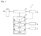
- a charging equipment 1 for a secondary battery 10 comprises: a power supply part 2 including a transformer-rectifier circuit for changing commercial alternating-current power into direct-current power, an operation switch 6 as an operation means for executing an operation such as start of charge by a user, a one-chip microcomputer (hereinafter referred to as one-chip micom) 4 as a control means for controlling charge of a secondary battery 10, a charge control circuit 5 serving as a charging means for applying the equilibrium voltage E eq at full charge or the special charging voltage E s higher than the equilibrium voltage E eq at full charge to the secondary battery 10, a LED (Light Emitting Diode) lamp 7 serving as an informational means for displaying a condition of being charging or finishing charging etc., a number of input and output terminals (not shown), and the like, wherein the one-chip micom 4 is connected to the power supply part 2, the operation switch 6, the charge control circuit 5, the LED
- the charging equipment comprises the LED lamp 7 as an example of the informational means for giving visual information of the condition of being charging or finishing charging etc., however, it may comprise another example of the informational means for giving auricular information by use of sound or voice etc.
- the charging equipment may comprise any type of the informational means.
- the one-chip micom 4 comprises a micro processing unit (hereinafter referred to as MPU) 40 serving as a central processing unit, a read only memory (hereinafter referred to as ROM) 41 serving as a storage means, a random access memory (hereinafter referred to as RAM) 42 serving as a storage means, a PWM 43 for controlling pulse width moderation, a timer 44 serving as a time clocking means, a counter 45 serving as a counting means, a current detection part 46 serving as a current detection means, and the like.
- MPU micro processing unit
- ROM read only memory
- RAM random access memory
- the equilibrium voltage E eq at full charge of the secondary battery 10 (see Fig.2) and the special voltage E s (referring to Fig.2, as the applied voltage is increased for charging the secondary battery 10 from its almost empty condition, the increasing rate of charging electric current to increasing applied voltage ( ⁇ I/ ⁇ E) becomes smaller and smaller, and finally the charging electric current reaches a peak value I so from which it can increase no more.
- the special voltage E s corresponds to the peak value I so of charging electric current out of the irreversible chemical reaction region D.) larger than the equilibrium voltage E eq of the secondary battery 10 are stored in the RAM 42.
- In the ROM 43 are programmed a program for judging whether the secondary battery 10 reaches its fully charged condition or not, and the like.
- the charge control circuit 5 comprises a charge voltage supply circuit for supplying the secondary battery 10 with the special charging voltage E s to which the voltage from the power supply part 2 is dropped down, a check voltage supply circuit for supplying the secondary battery 10 with the equilibrium voltage E eq at full charge to which the voltage from the power supply part 2 is dropped down, and a switch for switching applied voltage to the secondary battery 10 to the voltage selected from the group consisting of the special charging voltage E s supplied by the charge voltage supply circuit, and the equilibrium voltage E eq at full charge supplied by the check voltage supply circuit.
- one predetermined output terminal of the one-chip micom 4 is set as a terminal (output terminal for voltage-switching signals) for outputting a signal to switch voltage, so that, when the switch serving as a switch means receives the signal to switch voltage from the output terminal for voltage switch signal, applied voltage to the secondary battery 10 is switched to either the special charging voltage E s or the equilibrium voltage E eq at full charge.
- a resistance for detecting check current is interposed in the check voltage supply circuit, and a branch point positioned on the input-side of the resistance for detecting check current and another branch point positioned on the output-side of the resistance for detecting check current are connected to two predetermined input terminals (input terminals for current) of the one-chip micom 4 respectively, so that electric current (check current) flowing through the secondary battery 10 is detected by detecting the difference of two values of current each of which is inputted thorough each input terminal for current in the current detection part 46 of the micom 4.
- the above-mentioned switch is switched to the side of the check voltage supply circuit, when electric current (check current) flowing through the secondary battery 10 is detected by the difference of currents through the two input terminals for current during application of the equilibrium voltage E eq at full charge to the secondary battery 10.
- Fig. 2 shows voltage-current characteristic curves in a charged secondary battery 10 corresponding to different charging rates, with battery terminal voltage (applied voltage) E (V) as the abscissa, and charging electric current I (mA) as the ordinate.
- a graph ⁇ drawn in a dashed line in Fig.2 expresses a voltage-current characteristic during charge of the secondary battery 10 when its charging rate is approximately 0%.
- E ⁇ lower than the base voltage (nominal voltage) E 0 is applied, charging electric current starts to flow.
- This applied voltage (battery terminal voltage) when charging electric current starts to flow is defined as open-circuit voltage.
- a graph ⁇ drawn with a long dashed short dashed line in Fig.2 expresses a voltage-current characteristic during charge of the secondary battery 10 when its charging rate is approximately 50%.
- Open-circuit voltage E ⁇ for starting flow of electric current to be charged is applied higher than the open-circuit voltage E ⁇ for charging the secondary battery 10 when its charging rate is approximately 0%.
- a graph ⁇ drawn in a long dashed double-short dashed line in Fig.2 expresses a voltage-current characteristic during charge of the secondary battery 10 when its charging rate is approximately 90%, requiring open-circuit voltage E ⁇ higher than E ⁇ .
- a graph ⁇ drawn in a continuous line in Fig.2 expresses a voltage-current characteristic during charge of the secondary battery 10 when its charging rate is approximately (less than) 100%, requiring open-circuit voltage E ⁇ higher than E ⁇ .
- Open-circuit voltage for the secondary battery 10 when its charging rate is just 100% is equal to the equilibrium voltage E eq which is higher than E ⁇ .
- charging electric current starts to increase substantially in proportion to increase of applied voltage, and applied voltage passes over a certain voltage (an inflection point of the voltage-current curve), when the increase rate of charging electric current to applied voltage ( ⁇ I/ ⁇ E) begins to decrease. Finally, charging electric current does not increase any more even if applied voltage is increased, so that it reaches peak electric current I so .
- applied voltage corresponding to the peak electric current I so which is charging electric current when the increase rate of charging electric current to applied voltage ( ⁇ I/ ⁇ E) becomes zero, is the special charging voltage E s peculiar to each secondary battery 10, determined by a kind, a degraded state, and other element of the secondary battery 10 to be charged.
- the irreversible chemical reaction region D hatched in Fig. 2 is a region of the relationship between charging electric current and applied voltage such as to cause irreversible chemical reaction which is harmful to the secondary battery 10.
- the battery capacity of the secondary battery 10 is reckoned as product of charging electric current multiplied by charge time. Therefore, for shortening the charge time, it is necessary to increase charging electric current.
- Fig.2 when the equilibrium voltage E eq at full charge is applied to the secondary battery 10 of approximately 0% charging rate, charging electric current decreases from current I eqo ( ⁇ I so ) in proportion to increase of its charging rate.
- the charging electric current becomes 0mA when the secondary battery 1 reaches the fully charged condition, so that this condition facilitates easy judgment whether the secondary battery 10 is fully charged.
- the charging electric current during charging by use of the equilibrium voltage E eq at full charge is lower than that by use of the special charging voltage E s , so that charge time of charge by use of the equilibrium voltage E eq at full charge becomes considerably long.
- the special charging voltage E s is applied for the main charge so that such a large electric current flows through the secondary battery as the highest charging electric current (the peak electric current I so ) out of the irreversible chemical reaction region D, and at periodic intervals, the voltage applied to the secondary battery 10 is switched to the equilibrium voltage E eq at full charge so as to check whether the secondary battery 10 is fully charged or not.
- the voltage to be applied for charging the secondary battery 10 with large electric current is not limited to the special charging voltage E s corresponding to the peak electric current I so . It may be lower than the voltage E s so as to correspond to electric current smaller than the peak electric current I so .
- This conventional charging equipment 1 is a fundamental composition of the charging equipment 1 according to the present invention shown hereinafter.
- Fig.1 shows composition of the conventional charging equipment 1 according to the conventional invention.
- a judging program serving as a judging means for comparing check current i detected by the current detection part 46 during application of the equilibrium voltage E eq at full charge to the secondary battery 10 with a preset standard electric current J (e.g. 10mA) for finishing charging.
- a preset standard electric current J e.g. 10mA
- the ROM 41 of the one-chip micom 4 is a program for judging which is larger of the check current i and the standard electric current J.
- a user inputs a kind of secondary battery 10 to be charged to the one-chip micom 4 by manipulating the operation switch 6, thereby selecting the special charging voltage E s and equilibrium voltage E eq at full charge in correspondence to the kind of secondary battery 10 from a table in the RAM 42 in the one-chip micom 4.
- Both the special charging voltage E s and the equilibrium voltage E eq at full charge are determined according to the kind of the secondary battery such as the nickel-cadmium battery, the nickel metal hydride battery etc., the battery capacity, the size of the secondary battery, and the like.
- the equilibrium voltage E eq at full charge is set to around 1.41 V
- the special charging voltage E s is set to around 1.80V higher than the equilibrium voltage E eq .
- a user pushes the operation switch 6 so as to start charging [step A1], whereby the special charging voltage E s is applied to the secondary battery 10 for a predetermined time (e.g. 55 seconds) T 1 [step A2].
- the timer 4 clocks a lapse of the predetermined time T 1 , when applied voltage is switched to the equilibrium voltage E eq at full charge [step A3].
- Electric current i flowing through the secondary battery 10 is detected by the current detection part 46 in the ROM 41 of the one-chip micom 4 while the equilibrium voltage E eq at full charge is applied to the secondary battery 10 for a short time T 2 (e.g. 5 seconds) [step A4].
- the judging program in ROM 41 compares the detected electric current i with the standard electric current J for finishing charging [step A5]. When the detected electric current i is larger than the standard electric current J for finishing charging, the control step returns to the step A2, and the above steps (charge control) are repeated. Otherwise; when the detected electric current i is below or equal to the standard electric current J for finishing charging, it is recognized that the secondary battery 10 is fully charged, so as to stop charging the secondary battery 10 [step A6].
- the charging equipment 1 of the conventional invention can charge the secondary battery 10 appropriately through the process of full charge without causing excessive chemical reaction (oxidation-reduction reaction) in the secondary battery 10. Further, this charging equipment 1 can prevent the internal structure of the secondary battery 10 from being damaged, thereby increasing effective battery cycles of the secondary battery 10 by leaps and bounds. Moreover, at the time of main charge, the charging equipment 1 applies the special charging voltage E s higher than the equilibrium voltage E eq at full charge to the secondary battery 10 so as to make considerably high charging electric current flow through the secondary battery 10, thereby reducing charge time sharply.
- the conventional charging equipment 1 periodically applies the equilibrium voltage E eq at full charge to the secondary battery 10 so as to check whether the charging rate of the secondary battery 10 comes to 100% or not.
- the secondary batteries 10 of the same kind such as nickel-cadmium batteries, nickel metal hydride batteries, and the like
- the same size such as size AA batteries, size AAA batteries, and the like
- the secondary batteries 10 belonging to the same kind and the same size may have slightly difference in their battery capacities or their equilibrium voltages at full charge because of the difference of makers, manufacturing processes, or usage histories. Such difference of the secondary batteries 10 belonging to the same kind and the same size is more possible if they are made by a foreign maker. For this reason, it happens that the true equilibrium voltage at full charge of the secondary battery in charging is slightly different from the equilibrium voltage E eq at full charge set in the charging equipment 1, so that, after charging of the secondary batteries 10 of the same kind and the sake size by the conventional charging equipment 1, some of them may actually be 90% charged, and others may be overcharged beyond 100% charging rate.
- the charging equipment 1 of the present invention is improved as follows.
- Fig.1 also shows composition of the charging equipment 1 according to the present invention.
- the charging equipment 1 of the present invention has almost the same composition with the conventional equipment 1 except the one-chip micom 4 and the charge control circuit 5.
- the charging equipment 1 of the present invention in the RAM 42 of the one-chip micom 4 are stored a lowest check voltage E 0 lower than the lowest rated equilibrium voltage at full charge of those of secondary batteries 10 of all kinds intended for charging, a special charging voltage E t ( ⁇ E s ) that is higher than the highest rated equilibrium voltage at full charge of those of secondary batteries 10 of all kinds intended for charging but does not come into an irreversible chemical reaction region D, and a preset pitch of voltage ⁇ E.
- ROM 41 of the one-chip micom 4 is programmed a subroutine program which is additionally carried out in the above-mentioned pulse width modulation control by the PWM 43.
- the subroutine program increments (or decrements) the pulse width c ⁇ w of the pulse wave step by step, by incrementing (or decrementing) the valuable c by 1 from 1 to n whenever a later-discussed condition is met.
- the highest check voltage E n , the lowest check voltage E 0 , and the pitch of voltage ⁇ E are set so that the counted number n becomes an integer not smaller than 2.
- the one-chip micom 4 has a number of input and output terminals, and one predetermined terminal of them is set as a PWM output terminal 48 for outputting the pulse wave of the pulse width c ⁇ w modulated in the PWM 43.
- the charge control circuit 5 comprises a charge voltage supply circuit 56 for supplying the secondary battery 10 with the special charging voltage E t to which the voltage from the power supply part 2 is dropped down, a voltage increment circuit 50 for incrementing check voltage E c by the pitch of voltage ⁇ E from the lowest check voltage E 0 , and a check voltage supply circuit 57 for supplying the secondary battery 10 with the check voltage E c outputted from the voltage increment circuit 50, and a switch 58 for switching voltage applied to the secondary battery 10 between the special charging voltage E t supplied by the charge voltage supply circuit 56 and the check voltage E c supplied by the check voltage supply circuit 57.
- Another predetermined output terminal of the one-chip micom 4 is set for outputting a signal to switch voltage (output terminal for voltage-switching signals).
- the switch 58 serving as a switch means, when it receives the signal to switch voltage from the output terminal for voltage-switching signal, switches the applied voltage to the secondary battery 10 between the special charging voltage E t and the check voltage E c .
- a resistance for detecting check current is interposed in the check voltage supply circuit 57, and a branch point positioned on the input-side of the resistance for detecting check current and another branch point positioned on the output-side of the resistance for detecting check current are connected to two predetermined input terminals (input terminals for current) of the one-chip micom 4 respectively, so that electric current (check current) flowing through the secondary battery 10 is detected by detecting the difference of two values of current each of which is inputted through each input terminal for current in the current detection part 46 of the one-chip micom 4.
- the switch 58 is switched to the side of the check voltage supply circuit 57, when electric current (check current) flowing through the secondary battery 10 is detected by detecting a difference between the currents through the two input terminals for current during application of the check voltage E c to the secondary battery 10.
- the voltage increment device of the present invention serving as a voltage increment means for incrementing the check voltage E c by the pitch of voltage ⁇ E will be explained.
- the voltage increment device of the present invention comprises the one-chip micom 4 for outputting the pulse wave of the pulse width c ⁇ w modulated gradationally from the PWM output terminal 48, and a voltage increment circuit 50, so that the precious movement to increment the voltage with light load can be realized by the on-chip micom 4 with small capacity.
- a plurality of output terminals of the one-chip micom are set for voltage increment control.
- An example thereof has 30 steps of voltage from infimum voltage to supremum voltage in increments of a pitch of voltage.
- five output terminals of the one-chip micom are set for the voltage increment control because 2 5 is equal to 32( ⁇ 30), so that 30 kinds of ON/OFF signals can be outputted from the five output terminals, whereby 30 steps of voltage are incremented basing on these ON/OFF signals.
- the above-mentioned voltage increment device having five or six output terminals set for the voltage increment control causes large load applied to the one-chip micom. If the one-chip micom has a small capacity, it is disadvantageous in throughput speed of other charge control. This is the reason why the one-chip micom of the conventional voltage increment device has a large capacity. However, the one-chip micom with large capacity is expensive, thereby being disadvantageous in respect of cost.
- the present voltage increment device is invented so as to ensure the precious movement to increment the voltage with light load.
- the voltage increment device of the present invention comprises the one-chip micom 4 for outputting the pulse wave of the pulse width c ⁇ w modulated gradationally from the PWM output terminal 48, and the voltage increment circuit 50.
- the voltage increment circuit 50 is, for example, comprised as follows.
- the voltage increment circuit 50A comprises a supremum and infimum voltage supply circuit 51A for supplying supremum voltage E H and infimum voltage E L , a supremum and infimum voltage setting circuit 52A for inverting the maximum and minimum amplitudes of the pulse wave outputted from the output terminal to each other, and setting the maximum amplitude of the inverted pulse wave to the supremum voltage E H and the minimum amplitude of the inverted pulse wave to the infimum voltage E L , and an arithmetic circuit 53A for averaging the voltage of the pulse wave outputted from the supremum and infimum voltage setting circuit 52A and outputting a voltage made by base voltage minus the averaged voltage, wherein the valuable c in the PWM 43 of the one-chip micom 4 is incremented, so that the check voltage E c outputted from the arithmetic circuit 53A is incremented by
- n (E n -E 0 )/ ⁇ E.
- the valuable c in the PWM 43 of the one-chip micom 4 is increased from 1 to n in increments of 1, so that the check voltage E c outputted from the arithmetic circuit 53A is incremented from the lowest check voltage E 0 to the highest check voltage E n in increments of the pitch of voltage ⁇ E.
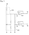
- Fig. 7 shows an example of the supremum and infimum voltage supply circuit 51A of the voltage increment circuit 50A.
- the supremum and infimum voltage supply circuit 51A comprises a shunt regulator 510, a first operational amplifier 511, and a second operational amplifier 512, wherein the power supply part 2 supplies predetermined voltage (e.g. 5V) to an input terminal 70 to the shunt regulator 510.
- This predetermined voltage is transformed into the supremum voltage E H and the infimum voltage E L in the shunt regulator 510, and the supremum voltage E H is outputted from one output terminal 71 of the shunt regulator 510 while the infimum voltage E L is outputted from the other output terminal 72 of it.
- the output terminal 71 is connected to a plus input terminal of the first operational amplifier 511, and a minus input terminal and an output terminal of the first operational amplifier 511 are connected.
- the output terminal of the first operational amplifier 511 is connected to a terminal 73.
- the supremum voltage E H is stabilized through the first operational amplifier 511, and outputted from the terminal 73.
- the output terminal 72 is connected to a plus input terminal of the second operational amplifier 512, and a minus input terminal and an output terminal of the second operational amplifier 512 are connected to each other.
- the output terminal of the second operational amplifier 512 is connected to a terminal 74.
- the infimum voltage E L is stabilized through the second operational amplifier 512, and outputted from the terminal 74.
- Fig. 8 shows an example of the supremum and infimum voltage setting circuit 52A and the arithmetic circuit 53A of the voltage increment circuit 50A.
- the above-mentioned supremum and infimum voltage supply circuit 51 A supplies the supremum voltage E H and the infimum voltage E L to the supremum and infimum voltage setting circuit 52A.
- the supremum and infimum voltage setting circuit 52A comprises an N-type field-effect transistor 521 and an electrical resistance 522.
- a gate of the transistor 521 is connected to the PWM output terminal 48 of the micom 4 through an electrical resistance 75, a source of the transistor 521 is connected to the terminal 74, and a drain of the transistor 521 is connected to the terminal through the electrical resistance 522.
- the PWM output terminal 48 of the one-chip micom 4 supplies the pulse wave of the pulse width c ⁇ w to the gate of the transistor 521, the terminal 73 supplies the supremum voltage E H to the drain of the transistor 521, and the terminal 74 drains the infimum voltage E L to the source of the transistor 521.
- the transistor 521 inverts the maximum and the minimum of amplitude of the pulse wave to each other, so that the maximum of amplitude of the inverted pulse wave serves as the supremum voltage E H and the minimum of amplitude of the inverted pulse wave serves as the infimum voltage E L .
- the arithmetic circuit 53A comprises an operational amplifier 531.
- an electrical resistance 532 and a condenser 533 are connected in parallel between a minus input terminal and an output terminal of the operational amplifier 531, and a electrical resistance 534 is connected to the minus input terminal of the operational amplifier 531 in series.
- the electrical resistance 534 is connected to a branch point 77 between the drain of transistor 521 and the electrical resistance 522.
- the output terminal of the operational amplifier 531 is connected to a terminal 79 connected to the check voltage supply circuit 57, the plus input terminal of the operational amplifier 531 is connected to a branch point 78 between the source of the transistor and the terminal 74, and the infimum voltage E L serves as the base voltage E B .
- the voltage of the pulse wave inputted from the supremum and infimum voltage setting circuit 52A is averaged, and a value of voltage made by the infimum voltage E L minus the just averaged voltage is outputted through the arithmetic circuit 53A, so that the value of voltage serves as the check voltage E c supplied to the check voltage supply circuit 57.
- the voltage increment circuit 50B comprises a supremum and infimum voltage supply circuit 51B for supplying supremum voltage E H and infimum voltage E L , a supremum and infimum voltage setting circuit 52B for setting the maximum of amplitude of the pulse wave outputted from the PWM output terminal 48 as the supremum voltage E H and the minimum of amplitude of the pulse wave as the infimum voltage E L , and an arithmetic circuit 53B for averaging the voltage of the pulse wave outputted from the supremum and infimum voltage setting circuit 52B and outputting a value of voltage made by base voltage E B plus the just averaged voltage, wherein the valuable c in the PWM 43 of the one-chip micom 4 is incremented, so that the check voltage E c outputted from the arithmetic circuit 53B is incremented by the pitch of voltage ⁇ E.
- n (E n -E 0 )/ ⁇ E.
- the valuable c in the PWM 43 of the one-chip micom 4 is increased from 1 to n in increments of 1, so that the check voltage E c outputted from the arithmetic circuit 53B is incremented from the lowest check voltage E 0 to the highest check voltage E n in increments of the pitch of voltage ⁇ E.
- the voltage increment circuit 50C according to the third embodiment comprises a supremum and infimum voltage supply circuit 51C for supplying supremum voltage E H and infimum voltage E L , a supremum and infimum voltage setting circuit 52C for inverting the maximum and the minimum of amplitude of the pulse wave outputted from the PWM output terminal 48 to each other, and setting the maximum of amplitude of the inverted pulse wave as the supremum voltage E H and the minimum of amplitude of the inverted pulse wave as the infimum voltage E L , and an arithmetic circuit 53C for averaging the voltage of the pulse wave outputted from the supremum and infimum voltage setting circuit 52C and outputting a value of voltage made by base voltage E B plus the just averaged voltage, wherein the valuable c in the PWM 43 of the one-chip micom 4 is decremented, so that the check voltage E c outputted from the arithmetic circuit 53C for averaging the voltage of the pulse wave outputted from the supremum and infim
- n (E n -E 0 )/ ⁇ E.
- the valuable c in the PWM 43 of the one-chip micom 4 is decremented from n to 1 in decrements of 1, so that the check voltage E c outputted from the arithmetic circuit 53B is incremented from the lowest check voltage E 0 to the highest check voltage E n in increments of the pitch of voltage ⁇ E.
- the voltage increment circuit 50D according to the fourth embodiment comprises a supremum and infimum voltage supply circuit 51D for supplying supremum voltage E H and infimum voltage E L , a supremum and infimum voltage setting circuit 52D for setting the maximum of amplitude of the pulse wave outputted from the PWM output terminal 48 as the supremum voltage E H and the minimum of amplitude of the pulse wave as the infimum voltage E L , and an arithmetic circuit 53D for averaging the voltage of the pulse wave outputted from the supremum and infimum voltage setting circuit 52D and outputting a value of voltage made by base voltage E B minus the just averaged voltage, wherein the valuable c in the PWM 43 of the one-chip micom 4 is decremented, so that the check voltage E c outputted from the arithmetic circuit 53D is incremented by the pitch of voltage ⁇ E.
- n (E n -E 0 )/ ⁇ E.
- the valuable c in the PWM 43 of the one-chip micom 4 is decremented from n to 1 in decrements of 1, so that the check voltage E c outputted from the arithmetic circuit 53D is incremented from the lowest check voltage E 0 to the highest check voltage E n in increments of the pitch of voltage ⁇ E.
- the voltage increment device is constructed as above mentioned, and it increments the check voltage E c from the lowest check voltage E 0 to the highest check voltage E n in increments of the pitch of voltage ⁇ E, by incrementing or decrementing the valuable c whenever a later-discussed condition is met.
- a first judging program for judging whether electric current i detected by the current detection part 46 during application of the check voltage E c to the secondary battery 10 is smaller than (or equal to) a preset standard electric current K for judging (e.g.
- a count program for detecting the points on the counter 45 which counts switching of applied voltage to the check voltage E c by the voltage control circuit 5 for the period from the last affirmative judgment (judgment that the detected electric current i during application of the check voltage E c-1 to the secondary battery 10 is smaller than (or equal to) the standard electric current K for judging) by the first judging program to the present affirmative judgment (judgment that the detected electric current i during application of the check voltage E c to the secondary battery 10 is smaller than (or equal to) the standard electric current K for judging) judged by the first judging program, and registering the points on the counter 45; and a second judging program for judging whether the counted number of switchings of the applied voltage to the check voltage E c for the period from the last affirmative judgment to the present affirmative judgment judged by the fist judging program is larger than r ( r is a real number not smaller than 1 and the best mode of r is that 1 ⁇ r ⁇ 2) times the
- the charging equipment 1 for a secondary battery of the present invention has the ROM 41 of the one-chip micom storing the first and second judging programs serving as judging means and the count program serving as count means.
- the count program and the second judging program are not limited to the above-mentioned.
- the count program may alternatively use the timer 44 for measuring the elapsed time from the last affirmative judgment judged by the first judging program to the present affirmative judgment judged by the first judging program, and the second judging program may alternatively judge whether the elapsed time from the last affirmative judgment judged by the first judging program to the present affirmative judgment by the first judging program is larger than r times the elapsed time from the before-last affirmative judgment to the last affirmative judgment.
- the charging by the charging equipment 1 for a secondary battery of the present invention is now compared to the high jump of athletics.
- an athlete whose high jump potential is not known precisely (a secondary battery whose equilibrium voltage at full charge is not known precisely).
- a bar is set to the lowest height (the voltage to be applied is set to the lowest check voltage E 0 ), and then he tries jumping (charging). If the athlete clears this lowest height (if the detected electric current i is smaller than (or equal to) the standard electric current K for judging at the judgment by the first judging program), the number of trials for clear of this height is registered. As concerns a general rule of the high jump, three trials are allowed. However, according to the assumed rule for this comparison, r times the number of trials for clearing the last set height (the last set check voltage E c-1 ) are allowed. It is supposed that r is set to 2.
- Fig.12 is a chart of an expanded portion pointed by an arrow P in Fig. 2. The situation will be represented by the case of a nickel-hydrogen battery.
- a voltage-current characteristic line is directed along an arrow in Fig.12 with the progress of charge (the upturn of charging rate), and reaches a reaction boundary Ld which is a point of 100% charging rate.
- the lowest check voltage E 0 is set to 1.40V.
- the battery is charged by the special charging voltage that is higher than equilibrium voltage E eq at full charge but does not come into the irreversible chemical reaction region D, and the charging condition of the battery is checked by the lowest check voltage E 0 . The charging and checking are repeated.
- the detected electric current i during each of the checks decreases so that it drops along a bold line on the scale of 1.40V in Fig. 12. For example, it is judged at the twentieth check by the lowest check voltage E 0 that the detected electric current i is smaller than (or equal to) the standard electric current K for judging.
- the voltage increment device sets the next check voltage E 1 to 1.41V made by the lowest check voltage E 0 plus 0.01V.
- this check voltage E 1 electric current that is a little less than 2mA flows through the nickel-hydrogen battery.
- the detected electric current i during the check decreases so that it drops along a dotted line on the scale of 1.41V in Fig. 12. For example, it is judged at the third check by the check voltage E 1 that the detected electric current i is smaller than (or equal to) the standard electric current K for judging.
- the voltage increment device sets the after-next check voltage E 2 to 1.42V made by the check voltage E 1 plus 0.01V.
- this check voltage E 2 about 2mA electric current flows through the nickel-hydrogen battery.
- the detected electric current i during check decreases so that it drops along a dotted line on the scale of 1.42V in Fig. 12. For example, it is judged at the third check by the check voltage E 2 that the detected electric current i is smaller than (or equal to) the standard electric current K for judging.
- the charging condition of the battery is checked similarly. If the number of checks by use of the check voltage 1.47V for getting the judgment that the detected electric current i is smaller than (or equal to) the standard electric current K for judging exceeds six, i.e., twice as large as the number of the last checks by use of the check voltage 1.46V for getting the judgment that the detected electric current i is smaller than (or equal to) the standard electric current K for judging, charge of the nickel-hydrogen battery is stopped. In this way, the secondary battery is charged till the charging rate of the secondary battery comes to approximately 100%.
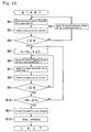
- a user sets a secondary battery 10 on the charging equipment 1, and manipulates the operation switch 6 so that the lowest check voltage E 0 which is lower than rated equilibrium voltage at full charge of a secondary battery of any kind and any size to be charged by the charging equipment 1 is applied to the secondary battery 10 for a short time (e.g. 5 seconds) T 2 [step B1].
- a short time e.g. 5 seconds
- the current detection part 46 detects electric current i flowing through the secondary battery 10 [step B2], and the first judging program is executed for judging about the detected electric current i [step B3].
- the switch 58 When the detected electric current i is larger than the standard electric current K for judging [step B3], the switch 58 is switched to change the applied voltage to the special charging voltage E t , and the special charging voltage E t is applied to the secondary battery 10 for a predetermined time (e.g. 55 seconds) T 1 [step B4].
- a predetermined time e.g. 55 seconds
- the switch 58 is switched to change the applied voltage to the lowest check voltage E 0 and the control step returns to the step B1.
- a predetermined time e.g. 55 seconds
- the switch 58 is switched to change the applied voltage to the renewed check voltage E c , and the renewed check voltage E c is applied to the secondary battery 10 for a short time T 2 [step B7].
- the current detection part 46 detects electric current i flowing through the secondary battery 10 [step B8], and the first judging program is executed to judge about the detected electric current i [step B9].
- the control step returns to the step B5. Otherwise, i.e., when the detected electric current i is smaller than (or equal to) the standard electric current K for judging [step B9], the counted number N c of the switchings to set the check voltage E c for the period from the last affirmative judgment (judgment that the detected electric current i is smaller than (or equal to) than the standard electric current K for judging) by the first judging program to the present affirmative judgment (judgment that the detected electric current i is smaller than (or equal to) the standard electric current K for judging) is judged by the second judging program [step B10].
- the counted number N c of switching is registered by the count program.
- the control step returns to the step B6.
- charge of the secondary battery 10 may be stopped immediately, or extra charge of electricity may be given to the secondary battery 10 for a certain time before charge of the secondary battery 10 is stopped.
- applied voltage is switched to the special charging voltage E t by the switch 58 and the special charging voltage E t is applied to the secondary battery 10 for a second predetermined time T 3 , then charge of the secondary battery 10 is finished.
- a cycle consisting of application of the special charging voltage E t for a predetermined time T 1 and application of the above-mentioned check voltage E c for a short time T 2 may be repeated predetermined times before charge of the secondary battery 10 is finished.
- the secondary battery 10 is charged, so that charging rate of the secondary battery can come closer to 100%.
- any secondary battery 10 regardless of the kind, size and so on, can have its own equilibrium voltage at full charge sought so as to be fully charged, whereby its charging rate becomes approximately 100%, thereby improving its reliability. Furthermore, even if the secondary battery 10 to be charged has an internal structure partially destroyed and degraded, the charging equipment 1 can seek the present equilibrium voltage at full charge of the secondary battery 10 so as to fully charge the secondary battery 10, whereby the charging rate of the secondary battery 10 becomes approximately 100%.
- Fig.14 illustrates three typical asymptotic function charts approaching respective fixed values.
- the function of Fig.14 (b) is not applicable to charge by the charging equipment 1 for a secondary battery of the present invention. Therefore, only the functions of Fig.14 (a) and Fig.14 (c) will be taken into account.
- the function of Fig.14 (a) will be explained.
- V eq,f electromotive voltage V eq (t) of the secondary battery is formulated with a following formula (a-1).
- V eq ( t ) ⁇ V eq,f - V eq ( t 0 ) ⁇ (1 - e - ⁇ ( t - t 0 ) ) + V eq ( t 0 )
- V eq (t 1 ) ⁇ V eq,f - V eq ( t 0 ) ⁇ (1- e - ⁇ ( t 1 - t 0 ) ) + V eq ( t 0 )
- a following formula (a-4) is the rearranged formula (a-3).
- the formula (a-2) is substituted for the formula (a-3)
- the formula (a-4) is expressed with a formula (a-5).
- a constant ⁇ is decided based on charging electric current, and an increment of compared voltage ⁇ V is 0.01V.
- the time t 1 serves as the base point of computation. (Even if the check voltage for start is set as 1.38V, the time to be controlled is after the time t 1 in Fig.16.)
- These values are substituted for respective constants in the formula (a-8).
- a following formula (a-9) is given.
- the lowest check voltage is set to 1.39V, and then charge of a secondary battery is started.
- the electromotive voltage of the secondary battery becomes 1.39V, it means that the voltage is equilibrated to that of the fully charged secondary battery, whereby charge of the secondary battery is halted.
- the check voltage is renewed by the increment of 0.01V so that the renewed check voltage becomes 1.40V.
- the battery electromotive voltage becomes 1.40V just after a certain time (in the example of Fig.17, dimensionless time 0.463) has passed.
- the check voltage is further renewed by the increment of 0.01V so that the renewed check voltage becomes 1.41V.
- any secondary battery can have a battery electromotive voltage precisely approaching its battery electromotive voltage at full charge, as long as the charging pattern of the secondary battery is as mentioned above. Therefore, any secondary battery can be fully charged regardless of a kind thereof.
- Fig.14 (c) the function of Fig.14 (c) will be explained.
- the battery voltage is equilibrated with the check voltage V eq (t 1 ) when the time t becomes t 1 .
- the check voltage is renewed by the increment of ⁇ V, and charge of the secondary battery is continued.
- the time required for equilibrating the battery electromotive voltage with the renewed check voltage is expressed as ⁇ t(t 1 ).
- Equilibrium voltage at this moment is expressed as V eq (t 1 )+ ⁇ V.
- the check voltage is further renewed by the increment of ⁇ V, and charge of the secondary battery is continued.
- a potential curve shown in Fig.18 represents a following formula (b-1) as mathematical deduction of the above-mentioned charge control.
- the formula (b-1) becomes a following formula (b-2) when a time t 1 is substituted for the variable time t.
- V eq ( t 1 ) ( V eq,f - V eq ,2' ) 1 1+ e - ⁇ ( t 1 - t c ) + V eq ,2'
- a following formula (B-2') is another transformation of the above formula (b-2).
- Formula (B-2') e - ⁇ ( t-t c ) V eq,f - V eq ( t ) V eq ( t ) - V eq ,2'
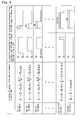
- the lowest check voltage compared to the first height of the bar is set to 1.40V.
- the dimensionless time required to clear the incremented voltage is 1.299.
- the time (dimensionless time 0.673) for increment of check voltage from 1.43V to 1.44V is the shortest in Fig. 19.
- the check voltage is further incremented, the time required to clear the further incremented check voltage becomes longer, and, if the worst comes to the worst, it may become too long to clear the check voltage. Therefore, it is decided that charge of the secondary battery is finished when the present charge time reaches twice the last time required for clear the check voltage.
- Target achievement rates of charging are drawn in the bottom cells of the table of Fig. 19. As shown in the table, according to this charging method, just after charge of a secondary battery is finished, the achievement rate of the charging reaches 99.97% of the proper electromotive voltage at full charge of the secondary battery.
- the charging method under such a setting of the constant r is also available that the secondary battery can be charged without reaching the irreversible chemical reaction region D, thereby increasing effective battery cycles of the charged secondary battery to five thousands times or more.
Applications Claiming Priority (5)
| Application Number | Priority Date | Filing Date | Title |
|---|---|---|---|
| JP2004049782 | 2004-02-25 | ||
| JP2004049782A JP3752249B2 (ja) | 2004-02-25 | 2004-02-25 | 二次電池の充電装置 |
| JP2004152146 | 2004-05-21 | ||
| JP2004152146A JP3869838B2 (ja) | 2004-05-21 | 2004-05-21 | 電圧値インクリメント装置を備えた二次電池の充電装置 |
| PCT/JP2004/008046 WO2005081378A1 (fr) | 2004-02-25 | 2004-06-09 | Chargeur de batterie secondaire |
Publications (3)
| Publication Number | Publication Date |
|---|---|
| EP1605573A1 true EP1605573A1 (fr) | 2005-12-14 |
| EP1605573A4 EP1605573A4 (fr) | 2006-04-12 |
| EP1605573B1 EP1605573B1 (fr) | 2009-12-16 |
Family
ID=34889378
Family Applications (1)
| Application Number | Title | Priority Date | Filing Date |
|---|---|---|---|
| EP04745721A Not-in-force EP1605573B1 (fr) | 2004-02-25 | 2004-06-09 | Chargeur de batterie secondaire |
Country Status (7)
| Country | Link |
|---|---|
| US (1) | US7075269B2 (fr) |
| EP (1) | EP1605573B1 (fr) |
| KR (1) | KR100665451B1 (fr) |
| CN (1) | CN100395939C (fr) |
| AT (1) | ATE452453T1 (fr) |
| DE (1) | DE602004024660D1 (fr) |
| WO (1) | WO2005081378A1 (fr) |
Cited By (2)
| Publication number | Priority date | Publication date | Assignee | Title |
|---|---|---|---|---|
| CN106169787A (zh) * | 2016-09-21 | 2016-11-30 | 联想(北京)有限公司 | 一种电子设备 |
| EP3007306A4 (fr) * | 2013-06-05 | 2017-01-18 | Kimree Hi-Tech Inc. | Procédé de charge de cigarette électronique et étui à cigarette électronique |
Families Citing this family (8)
| Publication number | Priority date | Publication date | Assignee | Title |
|---|---|---|---|---|
| CN100367627C (zh) * | 2002-05-17 | 2008-02-06 | 核心技术国际有限公司 | 充电电池的充电装置及充电方法 |
| JP5499872B2 (ja) * | 2010-04-21 | 2014-05-21 | ソニー株式会社 | バッテリー制御装置、バッテリー制御方法及びプログラム |
| KR100984556B1 (ko) | 2010-07-19 | 2010-09-30 | 주식회사 네이스코 | 황산화된 배터리를 복원하는 장치 및 방법 |
| CN102655344A (zh) * | 2011-03-02 | 2012-09-05 | 江苏嘉钰新能源技术有限公司 | 一种调整电池充电电压的电源和方法 |
| CN102938569B (zh) * | 2011-08-15 | 2017-06-27 | 联想(北京)有限公司 | 向电子设备供电的方法与装置、及电子设备 |
| US9147909B2 (en) | 2011-08-19 | 2015-09-29 | Samsung Sdi Co., Ltd. | Battery management system and method for synchronizing voltage and current of battery |
| KR102408274B1 (ko) * | 2016-04-08 | 2022-06-10 | 지배터리즈 에너지 캐나다 인코포레이티드 | 실시간 배터리 특성화에 기초한 배터리 충전 |
| US20220082630A1 (en) | 2019-01-15 | 2022-03-17 | Goiku Battery Co., Ltd. | Soh/soc detecting device for power storage element, and power storage element managing unit |
Citations (1)
| Publication number | Priority date | Publication date | Assignee | Title |
|---|---|---|---|---|
| WO2003098774A1 (fr) * | 2002-05-17 | 2003-11-27 | Techno Core International Co., Ltd. | Chargeur d'element secondaire et technique de charge |
Family Cites Families (6)
| Publication number | Priority date | Publication date | Assignee | Title |
|---|---|---|---|---|
| CN2098751U (zh) * | 1991-08-09 | 1992-03-11 | 广州高力电池有限公司 | 全自动电池充放电器 |
| US5442274A (en) * | 1992-08-27 | 1995-08-15 | Sanyo Electric Company, Ltd. | Rechargeable battery charging method |
| JP3402757B2 (ja) | 1994-06-16 | 2003-05-06 | 東芝電池株式会社 | 二次電池の充電方法および二次電池の充電装置 |
| JP3506916B2 (ja) * | 1998-07-03 | 2004-03-15 | 株式会社マキタ | 充電装置 |
| JP2001228225A (ja) * | 2000-02-17 | 2001-08-24 | Honda Motor Co Ltd | 蓄電装置の残容量検出装置 |
| JP3430439B2 (ja) * | 2000-12-22 | 2003-07-28 | 財団法人新産業創造研究機構 | 二次電池の充電方法及び二次電池の充電装置 |
-
2004
- 2004-06-09 KR KR1020047011071A patent/KR100665451B1/ko not_active IP Right Cessation
- 2004-06-09 DE DE602004024660T patent/DE602004024660D1/de active Active
- 2004-06-09 AT AT04745721T patent/ATE452453T1/de not_active IP Right Cessation
- 2004-06-09 WO PCT/JP2004/008046 patent/WO2005081378A1/fr active Application Filing
- 2004-06-09 CN CNB2004800011693A patent/CN100395939C/zh active Active
- 2004-06-09 US US10/517,820 patent/US7075269B2/en active Active
- 2004-06-09 EP EP04745721A patent/EP1605573B1/fr not_active Not-in-force
Patent Citations (1)
| Publication number | Priority date | Publication date | Assignee | Title |
|---|---|---|---|---|
| WO2003098774A1 (fr) * | 2002-05-17 | 2003-11-27 | Techno Core International Co., Ltd. | Chargeur d'element secondaire et technique de charge |
Non-Patent Citations (1)
| Title |
|---|
| See also references of WO2005081378A1 * |
Cited By (2)
| Publication number | Priority date | Publication date | Assignee | Title |
|---|---|---|---|---|
| EP3007306A4 (fr) * | 2013-06-05 | 2017-01-18 | Kimree Hi-Tech Inc. | Procédé de charge de cigarette électronique et étui à cigarette électronique |
| CN106169787A (zh) * | 2016-09-21 | 2016-11-30 | 联想(北京)有限公司 | 一种电子设备 |
Also Published As
| Publication number | Publication date |
|---|---|
| EP1605573A4 (fr) | 2006-04-12 |
| KR100665451B1 (ko) | 2007-01-04 |
| WO2005081378A1 (fr) | 2005-09-01 |
| CN1813386A (zh) | 2006-08-02 |
| ATE452453T1 (de) | 2010-01-15 |
| EP1605573B1 (fr) | 2009-12-16 |
| DE602004024660D1 (de) | 2010-01-28 |
| KR20060060519A (ko) | 2006-06-05 |
| US20050231163A1 (en) | 2005-10-20 |
| CN100395939C (zh) | 2008-06-18 |
| US7075269B2 (en) | 2006-07-11 |
Similar Documents
| Publication | Publication Date | Title |
|---|---|---|
| US7663344B2 (en) | Method for managing a pool of rechargeable batteries according to priority criteria determined based on a state of health of batteries | |
| EP0847123B1 (fr) | Procede de charge par impulsions et chargeur | |
| Koutroulis et al. | Novel battery charging regulation system for photovoltaic applications | |
| CN102804544B (zh) | 二次电池模块的充电控制装置和方法 | |
| US9172261B2 (en) | Battery pack, method of charging secondary battery and battery charger | |
| US8264198B2 (en) | Battery pack, battery charger and charging method having multiple charging modes | |
| US5596259A (en) | Method of charging a secondary battery | |
| EP2128958B1 (fr) | Procédé de coupure de courant pour batterie rechargeable et bloc-batterie l'utilisant | |
| AU2002211434B2 (en) | System and method for battery charging | |
| US9509164B2 (en) | Dynamic boost battery chargers | |
| CN101083402B (zh) | 可充电电池的充电方法和用于可充电电池的保护电路 | |
| US9780592B2 (en) | Battery pack for selectively setting a high capacity mode having a high charge capacity until a full charge of a secondary battery | |
| US20050194933A1 (en) | Method of charging a battery | |
| JP7145865B2 (ja) | 充電可能電池短絡予測装置および充電可能電池短絡予測方法 | |
| EP1605573B1 (fr) | Chargeur de batterie secondaire | |
| JPH09200968A (ja) | 組電池の充電制御装置 | |
| CN111525654A (zh) | 一种对电池组内各电池分时充电的电路及方法 | |
| JP3869838B2 (ja) | 電圧値インクリメント装置を備えた二次電池の充電装置 | |
| JP3752249B2 (ja) | 二次電池の充電装置 | |
| JP3009677B2 (ja) | 蓄電池監視装置 | |
| TWI807669B (zh) | 電池充放電試驗裝置及電池放電電力控制方法 | |
| JPH1174001A (ja) | 鉛蓄電池の充電方法 | |
| JPH07240234A (ja) | 二次電池の充電方法 |
Legal Events
| Date | Code | Title | Description |
|---|---|---|---|
| PUAI | Public reference made under article 153(3) epc to a published international application that has entered the european phase |
Free format text: ORIGINAL CODE: 0009012 |
|
| 17P | Request for examination filed |
Effective date: 20050901 |
|
| AK | Designated contracting states |
Kind code of ref document: A1 Designated state(s): AT BE BG CH CY CZ DE DK EE ES FI FR GB GR HU IE IT LI LU MC NL PL PT RO SE SI SK TR |
|
| AX | Request for extension of the european patent |
Extension state: AL HR LT LV MK |
|
| A4 | Supplementary search report drawn up and despatched |
Effective date: 20060227 |
|
| 17Q | First examination report despatched |
Effective date: 20070312 |
|
| DAX | Request for extension of the european patent (deleted) | ||
| GRAP | Despatch of communication of intention to grant a patent |
Free format text: ORIGINAL CODE: EPIDOSNIGR1 |
|
| GRAS | Grant fee paid |
Free format text: ORIGINAL CODE: EPIDOSNIGR3 |
|
| GRAA | (expected) grant |
Free format text: ORIGINAL CODE: 0009210 |
|
| AK | Designated contracting states |
Kind code of ref document: B1 Designated state(s): AT BE BG CH CY CZ DE DK EE ES FI FR GB GR HU IE IT LI LU MC NL PL PT RO SE SI SK TR |
|
| REG | Reference to a national code |
Ref country code: GB Ref legal event code: FG4D |
|
| REG | Reference to a national code |
Ref country code: CH Ref legal event code: EP |
|
| REG | Reference to a national code |
Ref country code: IE Ref legal event code: FG4D |
|
| REF | Corresponds to: |
Ref document number: 602004024660 Country of ref document: DE Date of ref document: 20100128 Kind code of ref document: P |
|
| REG | Reference to a national code |
Ref country code: SE Ref legal event code: TRGR |
|
| REG | Reference to a national code |
Ref country code: NL Ref legal event code: VDEP Effective date: 20091216 |
|
| RAP2 | Party data changed (patent owner data changed or rights of a patent transferred) |
Owner name: TECHNO CORE INTERNATIONAL CO., LTD. |
|
| PG25 | Lapsed in a contracting state [announced via postgrant information from national office to epo] |
Ref country code: SI Free format text: LAPSE BECAUSE OF FAILURE TO SUBMIT A TRANSLATION OF THE DESCRIPTION OR TO PAY THE FEE WITHIN THE PRESCRIBED TIME-LIMIT Effective date: 20091216 Ref country code: PL Free format text: LAPSE BECAUSE OF FAILURE TO SUBMIT A TRANSLATION OF THE DESCRIPTION OR TO PAY THE FEE WITHIN THE PRESCRIBED TIME-LIMIT Effective date: 20091216 |
|
| PG25 | Lapsed in a contracting state [announced via postgrant information from national office to epo] |
Ref country code: AT Free format text: LAPSE BECAUSE OF FAILURE TO SUBMIT A TRANSLATION OF THE DESCRIPTION OR TO PAY THE FEE WITHIN THE PRESCRIBED TIME-LIMIT Effective date: 20091216 |
|
| PG25 | Lapsed in a contracting state [announced via postgrant information from national office to epo] |
Ref country code: BG Free format text: LAPSE BECAUSE OF FAILURE TO SUBMIT A TRANSLATION OF THE DESCRIPTION OR TO PAY THE FEE WITHIN THE PRESCRIBED TIME-LIMIT Effective date: 20100316 Ref country code: ES Free format text: LAPSE BECAUSE OF FAILURE TO SUBMIT A TRANSLATION OF THE DESCRIPTION OR TO PAY THE FEE WITHIN THE PRESCRIBED TIME-LIMIT Effective date: 20100327 Ref country code: EE Free format text: LAPSE BECAUSE OF FAILURE TO SUBMIT A TRANSLATION OF THE DESCRIPTION OR TO PAY THE FEE WITHIN THE PRESCRIBED TIME-LIMIT Effective date: 20091216 Ref country code: NL Free format text: LAPSE BECAUSE OF FAILURE TO SUBMIT A TRANSLATION OF THE DESCRIPTION OR TO PAY THE FEE WITHIN THE PRESCRIBED TIME-LIMIT Effective date: 20091216 Ref country code: PT Free format text: LAPSE BECAUSE OF FAILURE TO SUBMIT A TRANSLATION OF THE DESCRIPTION OR TO PAY THE FEE WITHIN THE PRESCRIBED TIME-LIMIT Effective date: 20100416 Ref country code: RO Free format text: LAPSE BECAUSE OF FAILURE TO SUBMIT A TRANSLATION OF THE DESCRIPTION OR TO PAY THE FEE WITHIN THE PRESCRIBED TIME-LIMIT Effective date: 20091216 |
|
| PGFP | Annual fee paid to national office [announced via postgrant information from national office to epo] |
Ref country code: FI Payment date: 20100615 Year of fee payment: 7 Ref country code: FR Payment date: 20100706 Year of fee payment: 7 |
|
| PG25 | Lapsed in a contracting state [announced via postgrant information from national office to epo] |
Ref country code: BE Free format text: LAPSE BECAUSE OF FAILURE TO SUBMIT A TRANSLATION OF THE DESCRIPTION OR TO PAY THE FEE WITHIN THE PRESCRIBED TIME-LIMIT Effective date: 20091216 Ref country code: CZ Free format text: LAPSE BECAUSE OF FAILURE TO SUBMIT A TRANSLATION OF THE DESCRIPTION OR TO PAY THE FEE WITHIN THE PRESCRIBED TIME-LIMIT Effective date: 20091216 Ref country code: SK Free format text: LAPSE BECAUSE OF FAILURE TO SUBMIT A TRANSLATION OF THE DESCRIPTION OR TO PAY THE FEE WITHIN THE PRESCRIBED TIME-LIMIT Effective date: 20091216 |
|
| PLBE | No opposition filed within time limit |
Free format text: ORIGINAL CODE: 0009261 |
|
| STAA | Information on the status of an ep patent application or granted ep patent |
Free format text: STATUS: NO OPPOSITION FILED WITHIN TIME LIMIT |
|
| PG25 | Lapsed in a contracting state [announced via postgrant information from national office to epo] |
Ref country code: GR Free format text: LAPSE BECAUSE OF FAILURE TO SUBMIT A TRANSLATION OF THE DESCRIPTION OR TO PAY THE FEE WITHIN THE PRESCRIBED TIME-LIMIT Effective date: 20100317 Ref country code: CY Free format text: LAPSE BECAUSE OF FAILURE TO SUBMIT A TRANSLATION OF THE DESCRIPTION OR TO PAY THE FEE WITHIN THE PRESCRIBED TIME-LIMIT Effective date: 20091216 |
|
| 26N | No opposition filed |
Effective date: 20100917 |
|
| PGFP | Annual fee paid to national office [announced via postgrant information from national office to epo] |
Ref country code: GB Payment date: 20100618 Year of fee payment: 7 Ref country code: SE Payment date: 20100614 Year of fee payment: 7 |
|
| PG25 | Lapsed in a contracting state [announced via postgrant information from national office to epo] |
Ref country code: DK Free format text: LAPSE BECAUSE OF FAILURE TO SUBMIT A TRANSLATION OF THE DESCRIPTION OR TO PAY THE FEE WITHIN THE PRESCRIBED TIME-LIMIT Effective date: 20091216 Ref country code: MC Free format text: LAPSE BECAUSE OF NON-PAYMENT OF DUE FEES Effective date: 20100630 |
|
| REG | Reference to a national code |
Ref country code: CH Ref legal event code: PL |
|
| PG25 | Lapsed in a contracting state [announced via postgrant information from national office to epo] |
Ref country code: CH Free format text: LAPSE BECAUSE OF NON-PAYMENT OF DUE FEES Effective date: 20100630 Ref country code: IE Free format text: LAPSE BECAUSE OF NON-PAYMENT OF DUE FEES Effective date: 20100609 Ref country code: LI Free format text: LAPSE BECAUSE OF NON-PAYMENT OF DUE FEES Effective date: 20100630 |
|
| PGFP | Annual fee paid to national office [announced via postgrant information from national office to epo] |
Ref country code: IT Payment date: 20110219 Year of fee payment: 8 |
|
| PG25 | Lapsed in a contracting state [announced via postgrant information from national office to epo] |
Ref country code: FI Free format text: LAPSE BECAUSE OF NON-PAYMENT OF DUE FEES Effective date: 20110609 |
|
| REG | Reference to a national code |
Ref country code: SE Ref legal event code: EUG |
|
| GBPC | Gb: european patent ceased through non-payment of renewal fee |
Effective date: 20110609 |
|
| REG | Reference to a national code |
Ref country code: FR Ref legal event code: ST Effective date: 20120229 |
|
| PG25 | Lapsed in a contracting state [announced via postgrant information from national office to epo] |
Ref country code: FR Free format text: LAPSE BECAUSE OF NON-PAYMENT OF DUE FEES Effective date: 20110630 |
|
| PG25 | Lapsed in a contracting state [announced via postgrant information from national office to epo] |
Ref country code: GB Free format text: LAPSE BECAUSE OF NON-PAYMENT OF DUE FEES Effective date: 20110609 |
|
| PG25 | Lapsed in a contracting state [announced via postgrant information from national office to epo] |
Ref country code: HU Free format text: LAPSE BECAUSE OF FAILURE TO SUBMIT A TRANSLATION OF THE DESCRIPTION OR TO PAY THE FEE WITHIN THE PRESCRIBED TIME-LIMIT Effective date: 20100617 Ref country code: LU Free format text: LAPSE BECAUSE OF NON-PAYMENT OF DUE FEES Effective date: 20100609 |
|
| PG25 | Lapsed in a contracting state [announced via postgrant information from national office to epo] |
Ref country code: TR Free format text: LAPSE BECAUSE OF FAILURE TO SUBMIT A TRANSLATION OF THE DESCRIPTION OR TO PAY THE FEE WITHIN THE PRESCRIBED TIME-LIMIT Effective date: 20091216 |
|
| PG25 | Lapsed in a contracting state [announced via postgrant information from national office to epo] |
Ref country code: IT Free format text: LAPSE BECAUSE OF NON-PAYMENT OF DUE FEES Effective date: 20120609 |
|
| PG25 | Lapsed in a contracting state [announced via postgrant information from national office to epo] |
Ref country code: SE Free format text: LAPSE BECAUSE OF NON-PAYMENT OF DUE FEES Effective date: 20110610 |
|
| PGFP | Annual fee paid to national office [announced via postgrant information from national office to epo] |
Ref country code: DE Payment date: 20140630 Year of fee payment: 11 |
|
| REG | Reference to a national code |
Ref country code: DE Ref legal event code: R119 Ref document number: 602004024660 Country of ref document: DE |
|
| REG | Reference to a national code |
Ref country code: DE Ref legal event code: R119 Ref document number: 602004024660 Country of ref document: DE Effective date: 20150101 |
|
| PG25 | Lapsed in a contracting state [announced via postgrant information from national office to epo] |
Ref country code: DE Free format text: LAPSE BECAUSE OF NON-PAYMENT OF DUE FEES Effective date: 20150101 |