EP1605516A2 - Organic electro-luminescent display and method for manufacturing the same - Google Patents
Organic electro-luminescent display and method for manufacturing the same Download PDFInfo
- Publication number
- EP1605516A2 EP1605516A2 EP05012275A EP05012275A EP1605516A2 EP 1605516 A2 EP1605516 A2 EP 1605516A2 EP 05012275 A EP05012275 A EP 05012275A EP 05012275 A EP05012275 A EP 05012275A EP 1605516 A2 EP1605516 A2 EP 1605516A2
- Authority
- EP
- European Patent Office
- Prior art keywords
- spacer
- organic electro
- transparent substrate
- anode
- barrier
- Prior art date
- Legal status (The legal status is an assumption and is not a legal conclusion. Google has not performed a legal analysis and makes no representation as to the accuracy of the status listed.)
- Granted
Links
- 238000000034 method Methods 0.000 title claims abstract description 31
- 238000004519 manufacturing process Methods 0.000 title claims abstract description 26
- 239000000758 substrate Substances 0.000 claims abstract description 106
- 125000006850 spacer group Chemical group 0.000 claims description 78
- 230000004888 barrier function Effects 0.000 claims description 50
- 239000010408 film Substances 0.000 claims description 40
- 239000010409 thin film Substances 0.000 claims description 32
- 238000000059 patterning Methods 0.000 claims description 4
- 239000010410 layer Substances 0.000 description 29
- 239000004065 semiconductor Substances 0.000 description 9
- 238000002347 injection Methods 0.000 description 6
- 239000007924 injection Substances 0.000 description 6
- 150000002500 ions Chemical class 0.000 description 6
- 229910021420 polycrystalline silicon Inorganic materials 0.000 description 5
- 229920005591 polysilicon Polymers 0.000 description 5
- 230000008901 benefit Effects 0.000 description 4
- 239000004020 conductor Substances 0.000 description 4
- 239000012535 impurity Substances 0.000 description 4
- 239000011810 insulating material Substances 0.000 description 4
- 239000011229 interlayer Substances 0.000 description 4
- 239000011368 organic material Substances 0.000 description 3
- 239000004642 Polyimide Substances 0.000 description 2
- 229910052782 aluminium Inorganic materials 0.000 description 2
- XAGFODPZIPBFFR-UHFFFAOYSA-N aluminium Chemical compound [Al] XAGFODPZIPBFFR-UHFFFAOYSA-N 0.000 description 2
- 230000015572 biosynthetic process Effects 0.000 description 2
- 238000007796 conventional method Methods 0.000 description 2
- AMGQUBHHOARCQH-UHFFFAOYSA-N indium;oxotin Chemical compound [In].[Sn]=O AMGQUBHHOARCQH-UHFFFAOYSA-N 0.000 description 2
- 238000012986 modification Methods 0.000 description 2
- 230000004048 modification Effects 0.000 description 2
- 229920001721 polyimide Polymers 0.000 description 2
- 230000027756 respiratory electron transport chain Effects 0.000 description 2
- 239000000565 sealant Substances 0.000 description 2
- 238000007789 sealing Methods 0.000 description 2
- 238000012546 transfer Methods 0.000 description 2
- YVTHLONGBIQYBO-UHFFFAOYSA-N zinc indium(3+) oxygen(2-) Chemical compound [O--].[Zn++].[In+3] YVTHLONGBIQYBO-UHFFFAOYSA-N 0.000 description 2
- ZOXJGFHDIHLPTG-UHFFFAOYSA-N Boron Chemical compound [B] ZOXJGFHDIHLPTG-UHFFFAOYSA-N 0.000 description 1
- 229910052796 boron Inorganic materials 0.000 description 1
- 239000003990 capacitor Substances 0.000 description 1
- BHEPBYXIRTUNPN-UHFFFAOYSA-N hydridophosphorus(.) (triplet) Chemical compound [PH] BHEPBYXIRTUNPN-UHFFFAOYSA-N 0.000 description 1
- 238000005224 laser annealing Methods 0.000 description 1
- 230000002093 peripheral effect Effects 0.000 description 1
- 238000012545 processing Methods 0.000 description 1
- 230000002035 prolonged effect Effects 0.000 description 1
Images


Classifications
-
- H—ELECTRICITY
- H10—SEMICONDUCTOR DEVICES; ELECTRIC SOLID-STATE DEVICES NOT OTHERWISE PROVIDED FOR
- H10K—ORGANIC ELECTRIC SOLID-STATE DEVICES
- H10K59/00—Integrated devices, or assemblies of multiple devices, comprising at least one organic light-emitting element covered by group H10K50/00
- H10K59/10—OLED displays
- H10K59/12—Active-matrix OLED [AMOLED] displays
- H10K59/127—Active-matrix OLED [AMOLED] displays comprising two substrates, e.g. display comprising OLED array and TFT driving circuitry on different substrates
-
- H—ELECTRICITY
- H05—ELECTRIC TECHNIQUES NOT OTHERWISE PROVIDED FOR
- H05B—ELECTRIC HEATING; ELECTRIC LIGHT SOURCES NOT OTHERWISE PROVIDED FOR; CIRCUIT ARRANGEMENTS FOR ELECTRIC LIGHT SOURCES, IN GENERAL
- H05B33/00—Electroluminescent light sources
-
- H—ELECTRICITY
- H05—ELECTRIC TECHNIQUES NOT OTHERWISE PROVIDED FOR
- H05B—ELECTRIC HEATING; ELECTRIC LIGHT SOURCES NOT OTHERWISE PROVIDED FOR; CIRCUIT ARRANGEMENTS FOR ELECTRIC LIGHT SOURCES, IN GENERAL
- H05B33/00—Electroluminescent light sources
- H05B33/02—Details
- H05B33/04—Sealing arrangements, e.g. against humidity
-
- H—ELECTRICITY
- H05—ELECTRIC TECHNIQUES NOT OTHERWISE PROVIDED FOR
- H05B—ELECTRIC HEATING; ELECTRIC LIGHT SOURCES NOT OTHERWISE PROVIDED FOR; CIRCUIT ARRANGEMENTS FOR ELECTRIC LIGHT SOURCES, IN GENERAL
- H05B33/00—Electroluminescent light sources
- H05B33/12—Light sources with substantially two-dimensional radiating surfaces
- H05B33/26—Light sources with substantially two-dimensional radiating surfaces characterised by the composition or arrangement of the conductive material used as an electrode
-
- H—ELECTRICITY
- H10—SEMICONDUCTOR DEVICES; ELECTRIC SOLID-STATE DEVICES NOT OTHERWISE PROVIDED FOR
- H10K—ORGANIC ELECTRIC SOLID-STATE DEVICES
- H10K59/00—Integrated devices, or assemblies of multiple devices, comprising at least one organic light-emitting element covered by group H10K50/00
- H10K59/10—OLED displays
- H10K59/12—Active-matrix OLED [AMOLED] displays
- H10K59/122—Pixel-defining structures or layers, e.g. banks
-
- H—ELECTRICITY
- H10—SEMICONDUCTOR DEVICES; ELECTRIC SOLID-STATE DEVICES NOT OTHERWISE PROVIDED FOR
- H10K—ORGANIC ELECTRIC SOLID-STATE DEVICES
- H10K71/00—Manufacture or treatment specially adapted for the organic devices covered by this subclass
-
- H—ELECTRICITY
- H10—SEMICONDUCTOR DEVICES; ELECTRIC SOLID-STATE DEVICES NOT OTHERWISE PROVIDED FOR
- H10K—ORGANIC ELECTRIC SOLID-STATE DEVICES
- H10K71/00—Manufacture or treatment specially adapted for the organic devices covered by this subclass
- H10K71/40—Thermal treatment, e.g. annealing in the presence of a solvent vapour
Definitions
- the present invention relates to an organic electro-luminescent (EL) display, and more particularly, to a dual-panel type organic EL display and a method for manufacturing the same.
- EL organic electro-luminescent
- dual-panel type organic EL displays include a lower substrate, on which pixel switching elements and pixel driving elements are formed, and an upper substrate, on which an organic material is laminated.
- the upper and lower substrates are bonded to be electrically connected, for implementation of a display.
- the lower substrate of a dual-panel type organic EL display mainly includes, for each pixel region thereof, a switching thin film transistor (typically, a polysilicon thin film transistor) for switching of a pixel corresponding to the pixel region, a driving thin film transistor for driving of the pixel, a storage capacitor, and a pixel electrode.
- a switching thin film transistor typically, a polysilicon thin film transistor
- FIG. 1A is a sectional view illustrating a conventional process for manufacturing a lower substrate of a dual-panel type organic EL display. The following description will be given only in conjunction with one thin film transistor included in one pixel of the dual-panel type organic EL display.
- the semiconductor 2 is then patterned such that the semiconductor 2 remains only in a region where a thin film transistor is to be formed.
- a gate insulating film 3 and a conductive film for formation of a gate electrode are sequentially formed over the entire surface of the resulting structure.
- the conductive film is then patterned to form a gate electrode 4.
- impurity ions such as phosphorous (P) ions are then implanted into the semiconductor layer 2 which is, in turn, annealed to form source and drain regions 2a and 2c of the thin film transistor.
- P phosphorous
- an interlayer insulating film 5 is formed over the entire surface of the resulting structure. Subsequently, the interlayer insulating film 5 and gate insulating film 3 are selectively removed such that the source and drain regions 2a and 2c of the NMOS thin film transistor are exposed.
- An electrode line 6 and a pixel electrode 6' are then formed on the exposed source and drain regions 2a and 2c such that the electrode line 6 and pixel electrode 6' are electrically connected to the source and drain regions 2a and 2c, respectively.
- the lower substrate is completely formed.
- FIG. 2 is a plan view illustrating an upper substrate of the dual-panel type organic EL display manufactured in accordance with a conventional process.
- FIG. 1B is a cross-sectional view taken along the line I - I of FIG. 2.
- an anode 8 is formed on a transparent substrate 7.
- the anode 8 is made of a transparent conductive material having a high work function, such as indium tin oxide (ITO) or indium zinc oxide (IZO).
- an insulating film 9 is formed on a portion of the anode 8, using an insulating material such as polyimide.
- a barrier 10 is then formed on the insulating film 9.
- an island-shaped spacer 11 is formed on the anode 8 at a pixel region, using another insulating material.
- organic materials for a hole injection layer 12, a hole transfer layer 13, a light-emitting layer 14, an electron transfer layer 15, and an electron injection layer 16 are sequentially deposited over the entire surface of the resulting structure including the spacer 11.
- FIG. 1C is a sectional view illustrating a process for bonding the lower substrate of FIG. 1A and the upper substrate of FIG. 1B.
- the lower substrate of FIG. 1A and the upper substrate of FIG. 1B are bonded such that the cathode 17 formed on the spacer 11 in the upper substrate comes into contact with the pixel electrode 6' to be electrically connected.
- FIG. 1D is a sectional view illustrating a process for sealing the organic EL display in which the upper and lower substrates are bonded. As shown in FIG. 1D, vacuum is formed in a space defined between the bonded upper and lower substrates. Thereafter, the space between the upper and lower substrates is sealed, using a sealant 18.
- NMOS thin film transistors In the conventional organic EL display manufactured in the above-mentioned manner, NMOS thin film transistors must be used because each cathode in the upper substrate and the drain region of the corresponding driving thin film transistor in the lower substrate are electrically connected.
- the above-mentioned conventional EL display has a problem in that it is difficult to use a low-temperature polysilicon thin film transistor manufacturing process using a laser annealing method. This is because the low-temperature polysilicon thin film transistor is of a PMOS type.
- the conventional organic EL display cannot use PMOS thin film transistors which are more stable than NMOS thin film transistors.
- the present invention is directed to an organic EL display and a method for manufacturing the same that substantially obviate one or more problems due to limitations and disadvantages of the related art.
- An object of the present invention is to provide an organic EL display which can use PMOS thin film transistors, and a method for manufacturing the organic EL display.
- an organic electro-luminescent display comprises: a first transparent substrate and a second transparent substrate which are arranged to face each other while being spaced apart from each other by a predetermined distance; a transistor formed on the first transparent substrate; an anode formed on the second transparent substrate, and electrically connected to the transistor; an organic electro-luminescent layer formed on the anode; and a cathode formed on the organic electro-luminescent layer.
- the transistor may be a PMOS thin film transistor.
- the organic electro-luminescent display may further comprise a spacer formed around a light emitting region on the second transparent substrate, and a barrier formed around the spacer.
- the barrier may surround the spacer.
- the barrier may comprise stripe-shaped barriers respectively formed at opposite sides of the spacer such that the spacer is interposed between the stripe-shaped barriers.
- the spacer may be protruded to a level higher than the barrier.
- an organic electro-luminescent display comprises: a first transparent substrate and a second transparent substrate which are arranged to face each other while being spaced apart from each other by a predetermined distance; a transistor formed on the first transparent substrate; a spacer formed around a light emitting region on the second transparent substrate; an anode formed on the light emitting region of the second transparent substrate and the spacer such that the anode has a portion formed on the light emitting region, and a portion formed on the spacer, the anode portion formed on the spacer being electrically connected to the transistor; a barrier formed around the spacer; an organic electro-luminescent layer formed on the anode portion formed on the light emitting region of the second transparent substrate, except for the spacer; and a cathode formed on the organic electro-luminescent layer.
- the barrier may comprise a first barrier formed in a stripe on the anode at one side of the spacer, and a second barrier formed in a stripe on the second transparent substrate at the other side of the spacer.
- a method for manufacturing an organic electro-luminescent display comprises the steps of: manufacturing a lower substrate of the organic electro-luminescent display, the lower substrate manufacturing step comprising the steps of preparing a first transparent substrate, and forming a transistor on the first transparent substrate; manufacturing an upper substrate of the organic electro-luminescent display, the upper substrate manufacturing step comprising the steps of preparing a second transparent substrate, forming a spacer around a light emitting region on the second transparent substrate, forming an anode on the light emitting region of the second transparent substrate and the spacer, forming a barrier around the spacer, forming an organic electro-luminescent layer on a portion of the anode formed on the light emitting region of the second transparent substrate, except for the spacer, and forming a cathode on the organic electro-luminescent layer; and bonding the upper and lower plates of the organic electro-luminescent display such that a portion of the anode formed on the spacer in the upper substrate is electrically connected with an electrode of
- the step of forming the barrier around the spacer may comprise the steps of: forming an insulating film over an entire surface of the second transparent substrate including the anode, and patterning the insulating film such that the insulating film remains only around the spacer to surround the spacer; and forming a barrier on the remaining insulating film.
- the step of forming the barrier around the spacer may comprise the steps of: forming an insulating film over an entire surface of the second transparent substrate including the anode, and patterning the insulating film such that the insulating film remains to have stripe-shaped portions respectively arranged in parallel at opposite sides of the spacer to cause the spacer to be interposed between the stripe-shaped portions; and forming barriers on the remaining stripe-shaped insulating film portions.
- FIGs. 1A to 1D are sectional views illustrating a conventional method for manufacturing an organic EL display having a conventional structure
- FIG. 2 is a plan view illustrating an upper substrate of the convention organic EL display.
- FIGs. 3A to 3D are sectional views illustrating a method for manufacturing a dual-panel type organic EL display in accordance with the present invention.
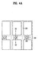
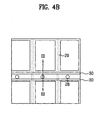
- FIGs. 4A and 4B are plan views illustrating upper substrates having different structures, which are used in the organic EL display according to the present invention, respectively.
- the present invention proposes a dual-panel type organic EL display having a structure capable of using PMOS thin film transistors, and a method for manufacturing the same.
- a PMOS thin film transistor is formed on one substrate of the dual-panel type organic EL display, as a device for driving of a pixel. Also, an organic EL element is formed on the other substrate. The substrates are then bonded such that an anode of the organic EL element and a pixel electrode of the PMOS thin film transistor are electrically connected.
- FIGs. 3A to 3E are sectional views illustrating sequential processing steps of a method for manufacturing a dual-panel type EL display in accordance with the present invention. The following description will be given only in conjunction with one thin film transistor included in one pixel of the organic EL display.
- FIG. 3A is a sectional view illustrating a process for manufacturing a lower substrate of the dual-panel type EL display. This process may be carried out in a conventional manner. In accordance with this process, first, a semiconductor layer 22 made of, for example, polysilicon, is formed over a first transparent substrate 21, as shown in FIG. 3A. The semiconductor layer 22 is then patterned to remain only in a region where a thin film transistor is to be formed.
- a semiconductor layer 22 made of, for example, polysilicon
- a gate insulating film 23 and a conductive film for formation of a gate electrode are sequentially formed over the entire surface of the resulting structure.
- the conductive film is then patterned to form a gate electrode 24.
- impurity ions such as boron (B) ions are then implanted into the semiconductor layer 22 which is, in turn, annealed to form source and drain regions 22a and 22c of the thin film transistor.
- B boron
- an interlayer insulating film 25 is formed over the entire surface of the resulting structure.
- the interlayer insulating film 25 and gate insulating film 23 are then selectively removed to expose the source and drain regions 22a and 22c of the PMOS thin film transistor.
- an electrode line 26 and a pixel electrode 26' are formed on the resulting structure such that the electrode line 26 and pixel electrode 26' are electrically connected to the source and drain regions 22a and 22c, respectively.
- a lower substrate is completely formed.
- FIGs. 4A and 4B are plan views illustrating an upper substrate of the dual-panel type organic EL display manufactured in accordance with the present invention.
- FIG. 3B is a cross-sectional view taken along the line II - II of FIG. 4A and the line III - III of FIG. 4B, illustrating an upper substrate manufacturing process according to the present invention.
- an island-shaped spacer 28 is first formed on a second transparent substrate 27, using an insulating material, as shown in FIG. 3B.
- the spacer 28 is arranged around a light emitting region.
- the spacer 28 is also shaped such that the lower portion of the spacer 28 is wider than the upper portion of the spacer 28.
- an anode 29 is formed on the second transparent substrate 27 including the spacer 28.
- the anode 29 is made of a transparent conductive material having a high work function, such as indium tin oxide (ITO) or indium zinc oxide (IZO).
- the anode 29 is formed only on the spacer 28 and the light emitting region of the second transparent substrate 27.
- an insulating film 30 is formed on a peripheral portion of the anode 29 and a region around the spacer 28, using an insulating material such as polyimide.
- a barrier 31 is then formed on the insulating film 30.
- the insulating film 30 and barrier 31 may be formed using one of two methods.
- the insulating film 30 is first formed over the entire surface of the structure including the anode 29, is then patterned such that the insulating film 30 remains only around the spacer 28 to surround the spacer 28.
- the barrier 31 is then formed on the remaining insulating film 30 such that the barrier 31 surrounds the spacer 28.
- the insulating film 30 is first formed over the entire surface of the structure including the anode 29, is then patterned such that the insulating film 30 remains to have stripe-shaped portions respectively arranged in parallel at opposite sides of the spacer 28.
- the barrier 31 is then formed on the remaining insulating film 30.
- the barrier 31 includes a first barrier formed in a stripe at one side of the spacer 28, and a second barrier formed in a stripe at the other side of the spacer 28.
- the first and second barriers are arranged in parallel in the form of parallel stripes at the opposite sides of the spacer 28, respectively, such that the spacer 28 is interposed between the first and second barriers.
- organic materials for a hole injection layer 32, a hole transfer layer 33, a light-emitting layer 34, an electron transfer layer 35, and an electron injection layer 36 are sequentially deposited over a portion of the anode 29 corresponding to the light emitting region of the second transparent substrate 27, except for the spacer 28.
- an organic EL layer is formed.
- a shadow mask is used in order to prevent the organic EL layer from being formed on the spacer 28.
- a cathode 37 which is made of a conductive material having a low work function, such as aluminum, is then deposited over the electron injection layer 36. Thus, an upper substrate is completely formed.
- the cathode 37 can be formed without using a shadow mask.
- a shadow mask is used in the process of forming the cathode 37, so as to prevent the cathode 37 from being formed on a region where no organic EL layer is formed between the stripe-shaped barriers.
- FIG. 3C is a sectional view illustrating a process for bonding the lower substrate of FIG. 3A and the upper substrate of FIG. 3B.
- the lower substrate of FIG. 3A and the upper substrate of FIG. 3B are bonded such that the anode 29 formed on the spacer 28 in the upper substrate comes into contact with the pixel electrode 26' of the lower substrate to be electrically connected.
- FIG. 3D is a sectional view illustrating a process for sealing the organic EL display in which the upper and lower substrates are bonded. As shown in FIG. 3D, a vacuum is formed in a space defined between the bonded upper and lower substrates. Thereafter, the space between the upper and lower substrates is sealed, using a sealant 38.
- the organic EL display of the present invention can use PMOS thin film transistors because the drain region of each driving thin film transistor formed on the lower substrate is electrically connected with the corresponding anode formed on the upper substrate.
Abstract
Description
- This application claims the benefit of Korean Patent Application No. 10-2004-0042635, filed on June 10, 2004, which is hereby incorporated by reference as if fully set forth herein.
- The present invention relates to an organic electro-luminescent (EL) display, and more particularly, to a dual-panel type organic EL display and a method for manufacturing the same.
- Generally, dual-panel type organic EL displays include a lower substrate, on which pixel switching elements and pixel driving elements are formed, and an upper substrate, on which an organic material is laminated. The upper and lower substrates are bonded to be electrically connected, for implementation of a display.
- Hereinafter, a conventional method for manufacturing such a dual-panel type organic EL display will be described.
- The lower substrate of a dual-panel type organic EL display mainly includes, for each pixel region thereof, a switching thin film transistor (typically, a polysilicon thin film transistor) for switching of a pixel corresponding to the pixel region, a driving thin film transistor for driving of the pixel, a storage capacitor, and a pixel electrode.
- FIG. 1A is a sectional view illustrating a conventional process for manufacturing a lower substrate of a dual-panel type organic EL display. The following description will be given only in conjunction with one thin film transistor included in one pixel of the dual-panel type organic EL display.
- In accordance with the conventional process, first, a
semiconductor layer 2 made of, for example, polysilicon, is formed over atransparent substrate 1, as shown in FIG. 1A. Thesemiconductor 2 is then patterned such that thesemiconductor 2 remains only in a region where a thin film transistor is to be formed. - Thereafter, a gate
insulating film 3 and a conductive film for formation of a gate electrode are sequentially formed over the entire surface of the resulting structure. The conductive film is then patterned to form agate electrode 4. - Using the
gate electrode 4 as a mask, impurity ions such as phosphorous (P) ions are then implanted into thesemiconductor layer 2 which is, in turn, annealed to form source anddrain regions - The portion of the
semiconductor layer 2, into which the impurity ions are not implanted, forms achannel region 2b of the NMOS thin film transistor. - Next, an interlayer insulating film 5 is formed over the entire surface of the resulting structure. Subsequently, the interlayer insulating film 5 and
gate insulating film 3 are selectively removed such that the source anddrain regions - An
electrode line 6 and a pixel electrode 6' are then formed on the exposed source anddrain regions electrode line 6 and pixel electrode 6' are electrically connected to the source anddrain regions - FIG. 2 is a plan view illustrating an upper substrate of the dual-panel type organic EL display manufactured in accordance with a conventional process. FIG. 1B is a cross-sectional view taken along the line I - I of FIG. 2.
- In accordance with the conventional process, as shown in FIGs. 1B and 2, an
anode 8 is formed on atransparent substrate 7. Theanode 8 is made of a transparent conductive material having a high work function, such as indium tin oxide (ITO) or indium zinc oxide (IZO). - Thereafter, an
insulating film 9 is formed on a portion of theanode 8, using an insulating material such as polyimide. Abarrier 10 is then formed on theinsulating film 9. - Next, an island-
shaped spacer 11 is formed on theanode 8 at a pixel region, using another insulating material. - Subsequently, organic materials for a
hole injection layer 12, ahole transfer layer 13, a light-emitting layer 14, anelectron transfer layer 15, and anelectron injection layer 16 are sequentially deposited over the entire surface of the resulting structure including thespacer 11. - A
cathode 17, which is made of a conductive material having a low work function, such as aluminum, is then deposited over theelectron injection layer 16. Thus, the upper substrate is completely formed. - FIG. 1C is a sectional view illustrating a process for bonding the lower substrate of FIG. 1A and the upper substrate of FIG. 1B.
- As shown in FIG. 1C, the lower substrate of FIG. 1A and the upper substrate of FIG. 1B are bonded such that the
cathode 17 formed on thespacer 11 in the upper substrate comes into contact with the pixel electrode 6' to be electrically connected. - FIG. 1D is a sectional view illustrating a process for sealing the organic EL display in which the upper and lower substrates are bonded. As shown in FIG. 1D, vacuum is formed in a space defined between the bonded upper and lower substrates. Thereafter, the space between the upper and lower substrates is sealed, using a
sealant 18. - In the conventional organic EL display manufactured in the above-mentioned manner, NMOS thin film transistors must be used because each cathode in the upper substrate and the drain region of the corresponding driving thin film transistor in the lower substrate are electrically connected.
- However, the above-mentioned conventional EL display has a problem in that it is difficult to use a low-temperature polysilicon thin film transistor manufacturing process using a laser annealing method. This is because the low-temperature polysilicon thin film transistor is of a PMOS type.
- For this reason, the conventional organic EL display cannot use PMOS thin film transistors which are more stable than NMOS thin film transistors.
- Accordingly, the present invention is directed to an organic EL display and a method for manufacturing the same that substantially obviate one or more problems due to limitations and disadvantages of the related art.
- An object of the present invention is to provide an organic EL display which can use PMOS thin film transistors, and a method for manufacturing the organic EL display.
- Additional advantages, objects, and features of the invention will be set forth in part in the description which follows and in part will become apparent to those having ordinary skill in the art upon examination of the following or may be learned from practice of the invention. The objectives and other advantages of the invention may be realized and attained by the structure particularly pointed out in the written description and claims hereof as well as the appended drawings.
- To achieve these objects and other advantages and in accordance with the purpose of the invention, as embodied and broadly described herein, an organic electro-luminescent display comprises: a first transparent substrate and a second transparent substrate which are arranged to face each other while being spaced apart from each other by a predetermined distance; a transistor formed on the first transparent substrate; an anode formed on the second transparent substrate, and electrically connected to the transistor; an organic electro-luminescent layer formed on the anode; and a cathode formed on the organic electro-luminescent layer.
- The transistor may be a PMOS thin film transistor. The organic electro-luminescent display may further comprise a spacer formed around a light emitting region on the second transparent substrate, and a barrier formed around the spacer.
- The barrier may surround the spacer. Alternatively, the barrier may comprise stripe-shaped barriers respectively formed at opposite sides of the spacer such that the spacer is interposed between the stripe-shaped barriers.
- The spacer may be protruded to a level higher than the barrier.
- In another aspect of the present invention, an organic electro-luminescent display comprises: a first transparent substrate and a second transparent substrate which are arranged to face each other while being spaced apart from each other by a predetermined distance; a transistor formed on the first transparent substrate; a spacer formed around a light emitting region on the second transparent substrate; an anode formed on the light emitting region of the second transparent substrate and the spacer such that the anode has a portion formed on the light emitting region, and a portion formed on the spacer, the anode portion formed on the spacer being electrically connected to the transistor; a barrier formed around the spacer; an organic electro-luminescent layer formed on the anode portion formed on the light emitting region of the second transparent substrate, except for the spacer; and a cathode formed on the organic electro-luminescent layer.
- The barrier may comprise a first barrier formed in a stripe on the anode at one side of the spacer, and a second barrier formed in a stripe on the second transparent substrate at the other side of the spacer.
- In another aspect of the present invention, a method for manufacturing an organic electro-luminescent display comprises the steps of: manufacturing a lower substrate of the organic electro-luminescent display, the lower substrate manufacturing step comprising the steps of preparing a first transparent substrate, and forming a transistor on the first transparent substrate; manufacturing an upper substrate of the organic electro-luminescent display, the upper substrate manufacturing step comprising the steps of preparing a second transparent substrate, forming a spacer around a light emitting region on the second transparent substrate, forming an anode on the light emitting region of the second transparent substrate and the spacer, forming a barrier around the spacer, forming an organic electro-luminescent layer on a portion of the anode formed on the light emitting region of the second transparent substrate, except for the spacer, and forming a cathode on the organic electro-luminescent layer; and bonding the upper and lower plates of the organic electro-luminescent display such that a portion of the anode formed on the spacer in the upper substrate is electrically connected with an electrode of the transistor in the lower substrate.
- The step of forming the barrier around the spacer may comprise the steps of: forming an insulating film over an entire surface of the second transparent substrate including the anode, and patterning the insulating film such that the insulating film remains only around the spacer to surround the spacer; and forming a barrier on the remaining insulating film.
- The step of forming the barrier around the spacer may comprise the steps of: forming an insulating film over an entire surface of the second transparent substrate including the anode, and patterning the insulating film such that the insulating film remains to have stripe-shaped portions respectively arranged in parallel at opposite sides of the spacer to cause the spacer to be interposed between the stripe-shaped portions; and forming barriers on the remaining stripe-shaped insulating film portions.
- It is to be understood that both the foregoing general description and the following detailed description of the present invention are exemplary and explanatory and are intended to provide further explanation of the invention as claimed.
- The accompanying drawings, which are included to provide a further understanding of the invention and are incorporated in and constitute a part of this application, illustrate embodiment(s) of the invention and together with the description serve to explain the principle of the invention. In the drawings:
- FIGs. 1A to 1D are sectional views illustrating a conventional method for manufacturing an organic EL display having a conventional structure;
- FIG. 2 is a plan view illustrating an upper substrate of the convention organic EL display.
- FIGs. 3A to 3D are sectional views illustrating a method for manufacturing a dual-panel type organic EL display in accordance with the present invention; and
- FIGs. 4A and 4B are plan views illustrating upper substrates having different structures, which are used in the organic EL display according to the present invention, respectively.
- Reference will now be made in detail to the preferred embodiments of the present invention, examples of which are illustrated in the accompanying drawings. Wherever possible, the same reference numbers will be used throughout the drawings to refer to the same or like parts.
- The present invention proposes a dual-panel type organic EL display having a structure capable of using PMOS thin film transistors, and a method for manufacturing the same.
- That is, in accordance with the present invention, a PMOS thin film transistor is formed on one substrate of the dual-panel type organic EL display, as a device for driving of a pixel. Also, an organic EL element is formed on the other substrate. The substrates are then bonded such that an anode of the organic EL element and a pixel electrode of the PMOS thin film transistor are electrically connected.
- FIGs. 3A to 3E are sectional views illustrating sequential processing steps of a method for manufacturing a dual-panel type EL display in accordance with the present invention. The following description will be given only in conjunction with one thin film transistor included in one pixel of the organic EL display.
- FIG. 3A is a sectional view illustrating a process for manufacturing a lower substrate of the dual-panel type EL display. This process may be carried out in a conventional manner. In accordance with this process, first, a
semiconductor layer 22 made of, for example, polysilicon, is formed over a firsttransparent substrate 21, as shown in FIG. 3A. Thesemiconductor layer 22 is then patterned to remain only in a region where a thin film transistor is to be formed. - Thereafter, a
gate insulating film 23 and a conductive film for formation of a gate electrode are sequentially formed over the entire surface of the resulting structure. The conductive film is then patterned to form agate electrode 24. - Using the
gate electrode 24 as a mask, impurity ions such as boron (B) ions are then implanted into thesemiconductor layer 22 which is, in turn, annealed to form source anddrain regions - The portion of the
semiconductor layer 22, into which the impurity ions are not implanted, forms achannel region 22b of the PMOS thin film transistor. - Next, an
interlayer insulating film 25 is formed over the entire surface of the resulting structure. Theinterlayer insulating film 25 andgate insulating film 23 are then selectively removed to expose the source anddrain regions - Thereafter, an
electrode line 26 and a pixel electrode 26' are formed on the resulting structure such that theelectrode line 26 and pixel electrode 26' are electrically connected to the source anddrain regions - FIGs. 4A and 4B are plan views illustrating an upper substrate of the dual-panel type organic EL display manufactured in accordance with the present invention. FIG. 3B is a cross-sectional view taken along the line II - II of FIG. 4A and the line III - III of FIG. 4B, illustrating an upper substrate manufacturing process according to the present invention.
- In accordance with the upper substrate manufacturing process, an island-shaped
spacer 28 is first formed on a secondtransparent substrate 27, using an insulating material, as shown in FIG. 3B. - The
spacer 28 is arranged around a light emitting region. Thespacer 28 is also shaped such that the lower portion of thespacer 28 is wider than the upper portion of thespacer 28. - Thereafter, an
anode 29 is formed on the secondtransparent substrate 27 including thespacer 28. Theanode 29 is made of a transparent conductive material having a high work function, such as indium tin oxide (ITO) or indium zinc oxide (IZO). - The
anode 29 is formed only on thespacer 28 and the light emitting region of the secondtransparent substrate 27. - Subsequently, an insulating
film 30 is formed on a peripheral portion of theanode 29 and a region around thespacer 28, using an insulating material such as polyimide. Abarrier 31 is then formed on the insulatingfilm 30. - The insulating
film 30 andbarrier 31 may be formed using one of two methods. - In accordance with the first method, the insulating
film 30 is first formed over the entire surface of the structure including theanode 29, is then patterned such that the insulatingfilm 30 remains only around thespacer 28 to surround thespacer 28. Thebarrier 31 is then formed on the remaining insulatingfilm 30 such that thebarrier 31 surrounds thespacer 28. - In accordance with the second method, the insulating
film 30 is first formed over the entire surface of the structure including theanode 29, is then patterned such that the insulatingfilm 30 remains to have stripe-shaped portions respectively arranged in parallel at opposite sides of thespacer 28. Thebarrier 31 is then formed on the remaining insulatingfilm 30. - In the latter case, the
barrier 31 includes a first barrier formed in a stripe at one side of thespacer 28, and a second barrier formed in a stripe at the other side of thespacer 28. The first and second barriers are arranged in parallel in the form of parallel stripes at the opposite sides of thespacer 28, respectively, such that thespacer 28 is interposed between the first and second barriers. - Thereafter, organic materials for a
hole injection layer 32, ahole transfer layer 33, a light-emittinglayer 34, anelectron transfer layer 35, and anelectron injection layer 36 are sequentially deposited over a portion of theanode 29 corresponding to the light emitting region of the secondtransparent substrate 27, except for thespacer 28. Thus, an organic EL layer is formed. - In the organic EL layer forming process, a shadow mask is used in order to prevent the organic EL layer from being formed on the
spacer 28. - A
cathode 37, which is made of a conductive material having a low work function, such as aluminum, is then deposited over theelectron injection layer 36. Thus, an upper substrate is completely formed. - Where the
barrier 31 has the structure of FIG. 4A, thecathode 37 can be formed without using a shadow mask. However, where thebarrier 31 has the structure of FIG. 4B, a shadow mask is used in the process of forming thecathode 37, so as to prevent thecathode 37 from being formed on a region where no organic EL layer is formed between the stripe-shaped barriers. - That is, in the latter case, it is necessary to expose the
anode 29 formed on thespacer 28, so as to enable theanode 29 to come into electrical contact with the pixel electrode 26' of the firsttransparent substrate 21. - FIG. 3C is a sectional view illustrating a process for bonding the lower substrate of FIG. 3A and the upper substrate of FIG. 3B.
- As shown in FIG. 3C, the lower substrate of FIG. 3A and the upper substrate of FIG. 3B are bonded such that the
anode 29 formed on thespacer 28 in the upper substrate comes into contact with the pixel electrode 26' of the lower substrate to be electrically connected. - FIG. 3D is a sectional view illustrating a process for sealing the organic EL display in which the upper and lower substrates are bonded. As shown in FIG. 3D, a vacuum is formed in a space defined between the bonded upper and lower substrates. Thereafter, the space between the upper and lower substrates is sealed, using a
sealant 38. - As apparent from the above description, the organic EL display of the present invention can use PMOS thin film transistors because the drain region of each driving thin film transistor formed on the lower substrate is electrically connected with the corresponding anode formed on the upper substrate.
- That is, in accordance with the present invention, it is possible to manufacture a dual-panel type organic EL display having an enhanced reliability and a prolonged life, by virtue of use of PMOS thin film transistors which are more stable than NMOS thin film transistors.
- It will be apparent to those skilled in the art that various modifications and variations can be made in the present invention without departing from the spirit or scope of the inventions. Thus, it is intended that the present invention covers the modifications and variations of this invention provided they come within the scope of the appended claims and their equivalents.
Claims (18)
- An organic electro-luminescent display comprising:a first transparent substrate and a second transparent substrate which are arranged to face each other while being spaced apart from each other by a predetermined distance;a transistor formed on the first transparent substrate;an anode formed on the second transparent substrate, and electrically connected to the transistor;an organic electro-luminescent layer formed on the anode; anda cathode formed on the organic electro-luminescent layer.
- The organic electro-luminescent display according to claim 1, wherein the transistor is a PMOS thin film transistor.
- The organic electro-luminescent display according to claim 1, further comprising:a spacer formed around a light emitting region on the second transparent substrate; anda barrier formed around the spacer.
- The organic electro-luminescent display according to claim 3, wherein the barrier surrounds the spacer.
- The organic electro-luminescent display according to claim 3, wherein the barrier comprises stripe-shaped barriers respectively formed at opposite sides of the spacer such that the spacer is interposed between the stripe-shaped barriers.
- The organic electro-luminescent display according to claim 3, wherein the spacer is protruded to a level higher than the barrier.
- An organic electro-luminescent display comprising:a first transparent substrate and a second transparent substrate which are arranged to face each other while being spaced apart from each other by a predetermined distance;a transistor formed on the first transparent substrate;a spacer formed around a light emitting region on the second transparent substrate;an anode formed on the light emitting region of the second transparent substrate and the spacer such that the anode has a portion formed on the light emitting region, and a portion formed on the spacer, the anode portion formed on the spacer being electrically connected to the transistor;a barrier formed around the spacer;an organic electro-luminescent layer formed on the anode portion formed on the light emitting region of the second transparent substrate, except for the spacer; anda cathode formed on the organic electro-luminescent layer.
- The organic electro-luminescent display according to claim 7, wherein the transistor is a PMOS thin film transistor.
- The organic electro-luminescent display according to claim 7, wherein the barrier surrounds the spacer.
- The organic electro-luminescent display according to claim 7, wherein the barrier comprises:a first barrier formed in a stripe on the anode at one side of the spacer; anda second barrier formed in a stripe on the second transparent substrate at the other side of the spacer.
- The organic electro-luminescent display according to claim 10, further comprising:an insulating film formed beneath the first and second barriers.
- The organic electro-luminescent display according to claim 10, wherein the first and second barriers are arranged in parallel at the opposite sides of the spacer such that the spacer is interposed between the first and second barriers.
- The organic electro-luminescent display according to claim 7, wherein the spacer is protruded to a level higher than the barrier.
- A method for manufacturing an organic electro-luminescent display, comprising the steps of:manufacturing a lower substrate of the organic electro-luminescent display, the lower substrate manufacturing step comprising the steps of preparing a first transparent substrate, and forming a transistor on the first transparent substrate;manufacturing an upper substrate of the organic electro-luminescent display, the upper substrate manufacturing step comprising the steps of preparing a second transparent substrate, forming a spacer around a light emitting region on the second transparent substrate, forming an anode on the light emitting region of the second transparent substrate and the spacer, forming a barrier around the spacer, forming an organic electro-luminescent layer on a portion of the anode formed on the light emitting region of the second transparent substrate, except for the spacer, and forming a cathode on the organic electro-luminescent layer; andbonding the upper and lower plates of the organic electro-luminescent display such that a portion of the anode formed on the spacer in the upper substrate is electrically connected with an electrode of the transistor in the lower substrate.
- The method according to claim 14, wherein the step of forming the barrier around the spacer comprises the steps of:forming an insulating film over an entire surface of the second transparent substrate including the anode, and patterning the insulating film such that the insulating film remains only around the spacer to surround the spacer; andforming a barrier on the remaining insulating film.
- The method according to claim 14, wherein the step of forming the barrier around the spacer comprises the steps of:forming an insulating film over an entire surface of the second transparent substrate including the anode, and patterning the insulating film such that the insulating film remains to have stripe-shaped portions respectively arranged in parallel at opposite sides of the spacer to cause the spacer to be interposed between the stripe-shaped portions; andforming barriers on the remaining stripe-shaped insulating film portions.
- The method according to claim 16, wherein the step of forming the cathode is executed using a shadow mask to prevent the cathode from being formed between the barriers.
- The method according to claim 14, wherein the step of forming the organic electro-luminescent layer is executed using a shadow mask to prevent the organic electro-luminescent layer from being formed on the spacer.
Applications Claiming Priority (2)
| Application Number | Priority Date | Filing Date | Title |
|---|---|---|---|
| KR1020040042635A KR100747569B1 (en) | 2004-06-10 | 2004-06-10 | Adhesive shape organic Electroluminescence display |
| KR2004042635 | 2004-06-10 |
Publications (3)
| Publication Number | Publication Date |
|---|---|
| EP1605516A2 true EP1605516A2 (en) | 2005-12-14 |
| EP1605516A3 EP1605516A3 (en) | 2008-12-17 |
| EP1605516B1 EP1605516B1 (en) | 2015-02-18 |
Family
ID=34982195
Family Applications (1)
| Application Number | Title | Priority Date | Filing Date |
|---|---|---|---|
| EP05012275.3A Active EP1605516B1 (en) | 2004-06-10 | 2005-06-08 | Organic electro-luminescent display and method for manufacturing the same |
Country Status (5)
| Country | Link |
|---|---|
| US (1) | US7586255B2 (en) |
| EP (1) | EP1605516B1 (en) |
| JP (1) | JP4925081B2 (en) |
| KR (1) | KR100747569B1 (en) |
| CN (1) | CN100456519C (en) |
Cited By (1)
| Publication number | Priority date | Publication date | Assignee | Title |
|---|---|---|---|---|
| US7211944B2 (en) * | 2002-12-13 | 2007-05-01 | Lg.Philips Lcd Co., Ltd. | Dual panel-type organic electroluminescent display device and method of fabricating the same |
Families Citing this family (10)
| Publication number | Priority date | Publication date | Assignee | Title |
|---|---|---|---|---|
| JP2005142054A (en) * | 2003-11-07 | 2005-06-02 | Seiko Epson Corp | Organic electroluminescence display device, manufacturing method of the organic electroluminescence display device, large-sized organic electroluminescence display, and electronic equipment |
| KR101157262B1 (en) * | 2005-12-14 | 2012-06-15 | 엘지디스플레이 주식회사 | Organic electro-luminescence display device and method for fabricating of the same |
| KR101294844B1 (en) | 2005-12-29 | 2013-08-08 | 엘지디스플레이 주식회사 | Fabricating method for organic electro-luminescence display device and organic electro-luminescence display device using the same |
| KR101274785B1 (en) * | 2006-06-30 | 2013-06-13 | 엘지디스플레이 주식회사 | organic electro-luminescence display device and method for fabricating the same |
| KR101291845B1 (en) * | 2006-12-13 | 2013-07-31 | 엘지디스플레이 주식회사 | Organic light emitting diodes display device and method of manufacturing the same |
| KR100922062B1 (en) * | 2008-02-15 | 2009-10-16 | 삼성모바일디스플레이주식회사 | Organic Light Emitting Display device |
| KR101427667B1 (en) * | 2008-07-04 | 2014-08-08 | 엘지디스플레이 주식회사 | organic electro-luminescent device |
| JP2010181534A (en) | 2009-02-04 | 2010-08-19 | Sumitomo Chemical Co Ltd | Substrate for display and method for manufacturing the same |
| JP2013025972A (en) * | 2011-07-20 | 2013-02-04 | Sumitomo Chemical Co Ltd | Display device and manufacturing method thereof |
| CN106449701A (en) * | 2016-09-19 | 2017-02-22 | 昆山工研院新型平板显示技术中心有限公司 | OLED panel and manufacturing method therefor |
Citations (2)
| Publication number | Priority date | Publication date | Assignee | Title |
|---|---|---|---|---|
| EP1220191A2 (en) | 2000-12-29 | 2002-07-03 | Samsung SDI Co., Ltd. | Organic electroluminescent display, driving method and pixel circuit thereof |
| US20020195961A1 (en) | 2001-06-22 | 2002-12-26 | International Business Machines Corporation | Organic light emitting devices |
Family Cites Families (29)
| Publication number | Priority date | Publication date | Assignee | Title |
|---|---|---|---|---|
| JP2848371B2 (en) * | 1997-02-21 | 1999-01-20 | 日本電気株式会社 | Organic EL display device and manufacturing method thereof |
| JP2002151252A (en) * | 2000-11-16 | 2002-05-24 | Stanley Electric Co Ltd | Organic el display device |
| US20030127972A1 (en) * | 2002-01-05 | 2003-07-10 | Cheng-Xian Han | Dual-panel active matrix organic electroluminscent display |
| JP2003208105A (en) * | 2002-01-10 | 2003-07-25 | Matsushita Electric Ind Co Ltd | Display device and manufacturing method therefor |
| JP2003249366A (en) * | 2002-02-22 | 2003-09-05 | Dainippon Printing Co Ltd | Organic electroluminescent image display device and its manufacturing method |
| KR100426964B1 (en) * | 2002-03-20 | 2004-04-13 | 엘지.필립스 엘시디 주식회사 | Organic Electroluminescent Device and Method for Fabricating the same |
| JP2003298611A (en) * | 2002-03-20 | 2003-10-17 | Youxun Sci & Technol Co Ltd | Network-monitoring system |
| JP2003282254A (en) * | 2002-03-22 | 2003-10-03 | Dainippon Printing Co Ltd | Image display device |
| JP3501148B2 (en) * | 2002-03-25 | 2004-03-02 | 富士電機ホールディングス株式会社 | Organic EL display |
| KR100464864B1 (en) * | 2002-04-25 | 2005-01-06 | 엘지.필립스 엘시디 주식회사 | Organic Electroluminescent Device and Method for Fabricating the same |
| KR100435054B1 (en) * | 2002-05-03 | 2004-06-07 | 엘지.필립스 엘시디 주식회사 | The organic electro-luminescence device and method for fabricating of the same |
| KR100465883B1 (en) * | 2002-05-03 | 2005-01-13 | 엘지.필립스 엘시디 주식회사 | The organic electro-luminescence device and method for fabricating of the same |
| JP2003332064A (en) * | 2002-05-09 | 2003-11-21 | Casio Comput Co Ltd | El panel and its manufacturing method |
| US7105999B2 (en) * | 2002-07-05 | 2006-09-12 | Lg.Philips Lcd Co., Ltd. | Organic electroluminescent display device and method of fabricating the same |
| KR100473591B1 (en) * | 2002-07-18 | 2005-03-10 | 엘지.필립스 엘시디 주식회사 | Dual Panel Type Organic Electroluminescent Device and Method for Fabricating the same |
| KR100473590B1 (en) * | 2002-07-25 | 2005-03-10 | 엘지.필립스 엘시디 주식회사 | The organic electro-luminescence device and method for fabricating of the same |
| KR100474000B1 (en) * | 2002-08-13 | 2005-03-10 | 엘지.필립스 엘시디 주식회사 | Dual Panel Type Organic Electroluminescent Device and Method for Fabricating the same |
| KR100544436B1 (en) * | 2002-11-26 | 2006-01-23 | 엘지.필립스 엘시디 주식회사 | The organic electro-luminescence device and method for fabricating of the same |
| TWI272872B (en) * | 2002-12-13 | 2007-02-01 | Lg Philips Lcd Co Ltd | Dual panel-type organic electroluminescent display device and method of fabricating the same |
| KR100484092B1 (en) * | 2002-12-26 | 2005-04-18 | 엘지.필립스 엘시디 주식회사 | Dual Panel Type Electroluminescent Device and Method for Fabricating the same |
| JP3915985B2 (en) * | 2003-08-22 | 2007-05-16 | セイコーエプソン株式会社 | Pixel element substrate, display device, electronic device, and manufacturing method of pixel element substrate |
| KR100621865B1 (en) * | 2003-12-29 | 2006-09-13 | 엘지.필립스 엘시디 주식회사 | Organic Electro-luminescence Display Device And Fabricating Method Thereof |
| JP2005203128A (en) * | 2004-01-13 | 2005-07-28 | Seiko Epson Corp | Electro-optical device and electronic equipment |
| JP2005228557A (en) * | 2004-02-12 | 2005-08-25 | Seiko Epson Corp | Manufacturing method of display unit, display unit and electronic equipment |
| JP2005228558A (en) * | 2004-02-12 | 2005-08-25 | Seiko Epson Corp | Manufacturing method of display unit, display unit, and electronic equipment |
| JP4225238B2 (en) * | 2004-04-21 | 2009-02-18 | セイコーエプソン株式会社 | Organic EL device manufacturing method, organic EL device, and electronic apparatus |
| KR100652352B1 (en) * | 2004-05-10 | 2006-12-01 | 엘지.필립스 엘시디 주식회사 | Organic Electro luminescence Device and fabrication method thereof |
| KR100606781B1 (en) * | 2004-06-04 | 2006-08-01 | 엘지전자 주식회사 | Dual Organic Electroluminescence display panel and Fabrication Method for the same |
| CN100515153C (en) * | 2004-10-12 | 2009-07-15 | 乐金显示有限公司 | Organic electro luminescence device and fabrication method thereof |
-
2004
- 2004-06-10 KR KR1020040042635A patent/KR100747569B1/en active IP Right Grant
-
2005
- 2005-06-08 EP EP05012275.3A patent/EP1605516B1/en active Active
- 2005-06-09 JP JP2005169846A patent/JP4925081B2/en active Active
- 2005-06-09 US US11/148,253 patent/US7586255B2/en active Active
- 2005-06-10 CN CNB2005100753543A patent/CN100456519C/en active Active
Patent Citations (2)
| Publication number | Priority date | Publication date | Assignee | Title |
|---|---|---|---|---|
| EP1220191A2 (en) | 2000-12-29 | 2002-07-03 | Samsung SDI Co., Ltd. | Organic electroluminescent display, driving method and pixel circuit thereof |
| US20020195961A1 (en) | 2001-06-22 | 2002-12-26 | International Business Machines Corporation | Organic light emitting devices |
Cited By (1)
| Publication number | Priority date | Publication date | Assignee | Title |
|---|---|---|---|---|
| US7211944B2 (en) * | 2002-12-13 | 2007-05-01 | Lg.Philips Lcd Co., Ltd. | Dual panel-type organic electroluminescent display device and method of fabricating the same |
Also Published As
| Publication number | Publication date |
|---|---|
| US20050275344A1 (en) | 2005-12-15 |
| CN1708200A (en) | 2005-12-14 |
| KR20050117344A (en) | 2005-12-14 |
| JP2005353600A (en) | 2005-12-22 |
| EP1605516A3 (en) | 2008-12-17 |
| CN100456519C (en) | 2009-01-28 |
| KR100747569B1 (en) | 2007-08-08 |
| JP4925081B2 (en) | 2012-04-25 |
| EP1605516B1 (en) | 2015-02-18 |
| US7586255B2 (en) | 2009-09-08 |
Similar Documents
| Publication | Publication Date | Title |
|---|---|---|
| US7586255B2 (en) | Organic electro-luminescent display of dual-panel type and method for manufacturing the same | |
| EP1667245B1 (en) | Organic electroluminescence display and method for manufacturing the same | |
| KR100709255B1 (en) | Flat panel display and method of manufacturing the same | |
| US6958252B2 (en) | Flat panel display device and method of manufacturing the same | |
| US9570529B2 (en) | Organic light emitting diode display | |
| CN101740607B (en) | Organic light emitting display device and method of manufacturing the same | |
| JP2001109404A (en) | El display device | |
| JP2001100654A (en) | El display device | |
| US8841832B2 (en) | Organic light emitting diode display having improved strength by preventing the exfoliation of a sealant | |
| JP4684592B2 (en) | Method for manufacturing organic electroluminescent device | |
| CN107845739B (en) | OLED device, OLED display panel and preparation method | |
| KR20090127715A (en) | Thin film transistor substrate, flat panel display including the same, and method of manufacturing the thin film transistor substrate | |
| US6850000B1 (en) | Thin film transistor organic light emitting diode structure | |
| KR100565674B1 (en) | Dual Organic Electroluminescence display panel and Fabrication Method for the same | |
| JP2001100655A (en) | El display device | |
| US6646308B2 (en) | Flat panel display device | |
| KR101202035B1 (en) | Light Emitting Diode and Method for preparing the same | |
| US9536936B2 (en) | Organic light emitting diode display | |
| TW525403B (en) | Electroluminescence display device | |
| JP4278244B2 (en) | EL display device | |
| KR100606781B1 (en) | Dual Organic Electroluminescence display panel and Fabrication Method for the same | |
| KR20150021212A (en) | Method for fabricating Organic Electroluminescence Device and the Organic Electroluminescence Device fabricated by the method | |
| KR100710351B1 (en) | Adhesive shape organic Electroluminescence display | |
| JP2001102165A (en) | El display | |
| KR20080104452A (en) | Organic electroluminescent device and methode for fabricating the same |
Legal Events
| Date | Code | Title | Description |
|---|---|---|---|
| PUAI | Public reference made under article 153(3) epc to a published international application that has entered the european phase |
Free format text: ORIGINAL CODE: 0009012 |
|
| 17P | Request for examination filed |
Effective date: 20050609 |
|
| AK | Designated contracting states |
Kind code of ref document: A2 Designated state(s): AT BE BG CH CY CZ DE DK EE ES FI FR GB GR HU IE IS IT LI LT LU MC NL PL PT RO SE SI SK TR |
|
| AX | Request for extension of the european patent |
Extension state: AL BA HR LV MK YU |
|
| RAP1 | Party data changed (applicant data changed or rights of an application transferred) |
Owner name: LG DISPLAY CO., LTD. |
|
| PUAL | Search report despatched |
Free format text: ORIGINAL CODE: 0009013 |
|
| AK | Designated contracting states |
Kind code of ref document: A3 Designated state(s): AT BE BG CH CY CZ DE DK EE ES FI FR GB GR HU IE IS IT LI LT LU MC NL PL PT RO SE SI SK TR |
|
| AX | Request for extension of the european patent |
Extension state: AL BA HR LV MK YU |
|
| AKX | Designation fees paid |
Designated state(s): AT BE BG CH CY CZ DE DK EE ES FI FR GB GR HU IE IS IT LI LT LU MC NL PL PT RO SE SI SK TR |
|
| 17Q | First examination report despatched |
Effective date: 20090804 |
|
| R17C | First examination report despatched (corrected) |
Effective date: 20090806 |
|
| REG | Reference to a national code |
Ref country code: DE Ref legal event code: R079 Ref document number: 602005045829 Country of ref document: DE Free format text: PREVIOUS MAIN CLASS: H01L0027150000 Ipc: H01L0027320000 |
|
| GRAP | Despatch of communication of intention to grant a patent |
Free format text: ORIGINAL CODE: EPIDOSNIGR1 |
|
| RIC1 | Information provided on ipc code assigned before grant |
Ipc: H01L 27/32 20060101AFI20140603BHEP Ipc: H01L 51/56 20060101ALI20140603BHEP |
|
| GRAJ | Information related to disapproval of communication of intention to grant by the applicant or resumption of examination proceedings by the epo deleted |
Free format text: ORIGINAL CODE: EPIDOSDIGR1 |
|
| GRAP | Despatch of communication of intention to grant a patent |
Free format text: ORIGINAL CODE: EPIDOSNIGR1 |
|
| INTG | Intention to grant announced |
Effective date: 20140703 |
|
| INTG | Intention to grant announced |
Effective date: 20140722 |
|
| GRAS | Grant fee paid |
Free format text: ORIGINAL CODE: EPIDOSNIGR3 |
|
| RAP1 | Party data changed (applicant data changed or rights of an application transferred) |
Owner name: LG DISPLAY CO., LTD. |
|
| GRAA | (expected) grant |
Free format text: ORIGINAL CODE: 0009210 |
|
| AK | Designated contracting states |
Kind code of ref document: B1 Designated state(s): AT BE BG CH CY CZ DE DK EE ES FI FR GB GR HU IE IS IT LI LT LU MC NL PL PT RO SE SI SK TR |
|
| REG | Reference to a national code |
Ref country code: GB Ref legal event code: FG4D |
|
| REG | Reference to a national code |
Ref country code: CH Ref legal event code: EP |
|
| REG | Reference to a national code |
Ref country code: AT Ref legal event code: REF Ref document number: 710952 Country of ref document: AT Kind code of ref document: T Effective date: 20150315 |
|
| REG | Reference to a national code |
Ref country code: IE Ref legal event code: FG4D |
|
| REG | Reference to a national code |
Ref country code: DE Ref legal event code: R096 Ref document number: 602005045829 Country of ref document: DE Effective date: 20150402 |
|
| REG | Reference to a national code |
Ref country code: NL Ref legal event code: VDEP Effective date: 20150218 |
|
| REG | Reference to a national code |
Ref country code: AT Ref legal event code: MK05 Ref document number: 710952 Country of ref document: AT Kind code of ref document: T Effective date: 20150218 |
|
| REG | Reference to a national code |
Ref country code: LT Ref legal event code: MG4D |
|
| PG25 | Lapsed in a contracting state [announced via postgrant information from national office to epo] |
Ref country code: SE Free format text: LAPSE BECAUSE OF FAILURE TO SUBMIT A TRANSLATION OF THE DESCRIPTION OR TO PAY THE FEE WITHIN THE PRESCRIBED TIME-LIMIT Effective date: 20150218 Ref country code: FI Free format text: LAPSE BECAUSE OF FAILURE TO SUBMIT A TRANSLATION OF THE DESCRIPTION OR TO PAY THE FEE WITHIN THE PRESCRIBED TIME-LIMIT Effective date: 20150218 Ref country code: LT Free format text: LAPSE BECAUSE OF FAILURE TO SUBMIT A TRANSLATION OF THE DESCRIPTION OR TO PAY THE FEE WITHIN THE PRESCRIBED TIME-LIMIT Effective date: 20150218 Ref country code: ES Free format text: LAPSE BECAUSE OF FAILURE TO SUBMIT A TRANSLATION OF THE DESCRIPTION OR TO PAY THE FEE WITHIN THE PRESCRIBED TIME-LIMIT Effective date: 20150218 |
|
| PG25 | Lapsed in a contracting state [announced via postgrant information from national office to epo] |
Ref country code: AT Free format text: LAPSE BECAUSE OF FAILURE TO SUBMIT A TRANSLATION OF THE DESCRIPTION OR TO PAY THE FEE WITHIN THE PRESCRIBED TIME-LIMIT Effective date: 20150218 Ref country code: IS Free format text: LAPSE BECAUSE OF FAILURE TO SUBMIT A TRANSLATION OF THE DESCRIPTION OR TO PAY THE FEE WITHIN THE PRESCRIBED TIME-LIMIT Effective date: 20150618 Ref country code: GR Free format text: LAPSE BECAUSE OF FAILURE TO SUBMIT A TRANSLATION OF THE DESCRIPTION OR TO PAY THE FEE WITHIN THE PRESCRIBED TIME-LIMIT Effective date: 20150519 Ref country code: NL Free format text: LAPSE BECAUSE OF FAILURE TO SUBMIT A TRANSLATION OF THE DESCRIPTION OR TO PAY THE FEE WITHIN THE PRESCRIBED TIME-LIMIT Effective date: 20150218 |
|
| PG25 | Lapsed in a contracting state [announced via postgrant information from national office to epo] |
Ref country code: SK Free format text: LAPSE BECAUSE OF FAILURE TO SUBMIT A TRANSLATION OF THE DESCRIPTION OR TO PAY THE FEE WITHIN THE PRESCRIBED TIME-LIMIT Effective date: 20150218 Ref country code: RO Free format text: LAPSE BECAUSE OF FAILURE TO SUBMIT A TRANSLATION OF THE DESCRIPTION OR TO PAY THE FEE WITHIN THE PRESCRIBED TIME-LIMIT Effective date: 20150218 Ref country code: DK Free format text: LAPSE BECAUSE OF FAILURE TO SUBMIT A TRANSLATION OF THE DESCRIPTION OR TO PAY THE FEE WITHIN THE PRESCRIBED TIME-LIMIT Effective date: 20150218 Ref country code: CZ Free format text: LAPSE BECAUSE OF FAILURE TO SUBMIT A TRANSLATION OF THE DESCRIPTION OR TO PAY THE FEE WITHIN THE PRESCRIBED TIME-LIMIT Effective date: 20150218 Ref country code: EE Free format text: LAPSE BECAUSE OF FAILURE TO SUBMIT A TRANSLATION OF THE DESCRIPTION OR TO PAY THE FEE WITHIN THE PRESCRIBED TIME-LIMIT Effective date: 20150218 |
|
| REG | Reference to a national code |
Ref country code: DE Ref legal event code: R097 Ref document number: 602005045829 Country of ref document: DE |
|
| PG25 | Lapsed in a contracting state [announced via postgrant information from national office to epo] |
Ref country code: PL Free format text: LAPSE BECAUSE OF FAILURE TO SUBMIT A TRANSLATION OF THE DESCRIPTION OR TO PAY THE FEE WITHIN THE PRESCRIBED TIME-LIMIT Effective date: 20150218 |
|
| PLBE | No opposition filed within time limit |
Free format text: ORIGINAL CODE: 0009261 |
|
| STAA | Information on the status of an ep patent application or granted ep patent |
Free format text: STATUS: NO OPPOSITION FILED WITHIN TIME LIMIT |
|
| PG25 | Lapsed in a contracting state [announced via postgrant information from national office to epo] |
Ref country code: IT Free format text: LAPSE BECAUSE OF FAILURE TO SUBMIT A TRANSLATION OF THE DESCRIPTION OR TO PAY THE FEE WITHIN THE PRESCRIBED TIME-LIMIT Effective date: 20150218 |
|
| 26N | No opposition filed |
Effective date: 20151119 |
|
| PG25 | Lapsed in a contracting state [announced via postgrant information from national office to epo] |
Ref country code: MC Free format text: LAPSE BECAUSE OF FAILURE TO SUBMIT A TRANSLATION OF THE DESCRIPTION OR TO PAY THE FEE WITHIN THE PRESCRIBED TIME-LIMIT Effective date: 20150218 |
|
| REG | Reference to a national code |
Ref country code: CH Ref legal event code: PL |
|
| PG25 | Lapsed in a contracting state [announced via postgrant information from national office to epo] |
Ref country code: LU Free format text: LAPSE BECAUSE OF FAILURE TO SUBMIT A TRANSLATION OF THE DESCRIPTION OR TO PAY THE FEE WITHIN THE PRESCRIBED TIME-LIMIT Effective date: 20150608 Ref country code: SI Free format text: LAPSE BECAUSE OF FAILURE TO SUBMIT A TRANSLATION OF THE DESCRIPTION OR TO PAY THE FEE WITHIN THE PRESCRIBED TIME-LIMIT Effective date: 20150218 |
|
| REG | Reference to a national code |
Ref country code: IE Ref legal event code: MM4A |
|
| REG | Reference to a national code |
Ref country code: FR Ref legal event code: PLFP Year of fee payment: 12 |
|
| PG25 | Lapsed in a contracting state [announced via postgrant information from national office to epo] |
Ref country code: LI Free format text: LAPSE BECAUSE OF NON-PAYMENT OF DUE FEES Effective date: 20150630 Ref country code: CH Free format text: LAPSE BECAUSE OF NON-PAYMENT OF DUE FEES Effective date: 20150630 Ref country code: IE Free format text: LAPSE BECAUSE OF NON-PAYMENT OF DUE FEES Effective date: 20150608 |
|
| PG25 | Lapsed in a contracting state [announced via postgrant information from national office to epo] |
Ref country code: BE Free format text: LAPSE BECAUSE OF FAILURE TO SUBMIT A TRANSLATION OF THE DESCRIPTION OR TO PAY THE FEE WITHIN THE PRESCRIBED TIME-LIMIT Effective date: 20150218 |
|
| REG | Reference to a national code |
Ref country code: FR Ref legal event code: PLFP Year of fee payment: 13 |
|
| PG25 | Lapsed in a contracting state [announced via postgrant information from national office to epo] |
Ref country code: BG Free format text: LAPSE BECAUSE OF FAILURE TO SUBMIT A TRANSLATION OF THE DESCRIPTION OR TO PAY THE FEE WITHIN THE PRESCRIBED TIME-LIMIT Effective date: 20150218 Ref country code: HU Free format text: LAPSE BECAUSE OF FAILURE TO SUBMIT A TRANSLATION OF THE DESCRIPTION OR TO PAY THE FEE WITHIN THE PRESCRIBED TIME-LIMIT; INVALID AB INITIO Effective date: 20050608 |
|
| PG25 | Lapsed in a contracting state [announced via postgrant information from national office to epo] |
Ref country code: CY Free format text: LAPSE BECAUSE OF FAILURE TO SUBMIT A TRANSLATION OF THE DESCRIPTION OR TO PAY THE FEE WITHIN THE PRESCRIBED TIME-LIMIT Effective date: 20150218 |
|
| PG25 | Lapsed in a contracting state [announced via postgrant information from national office to epo] |
Ref country code: TR Free format text: LAPSE BECAUSE OF FAILURE TO SUBMIT A TRANSLATION OF THE DESCRIPTION OR TO PAY THE FEE WITHIN THE PRESCRIBED TIME-LIMIT Effective date: 20150218 |
|
| REG | Reference to a national code |
Ref country code: FR Ref legal event code: PLFP Year of fee payment: 14 |
|
| PG25 | Lapsed in a contracting state [announced via postgrant information from national office to epo] |
Ref country code: PT Free format text: LAPSE BECAUSE OF FAILURE TO SUBMIT A TRANSLATION OF THE DESCRIPTION OR TO PAY THE FEE WITHIN THE PRESCRIBED TIME-LIMIT Effective date: 20150218 |
|
| REG | Reference to a national code |
Ref country code: DE Ref legal event code: R079 Ref document number: 602005045829 Country of ref document: DE Free format text: PREVIOUS MAIN CLASS: H01L0027320000 Ipc: H10K0059000000 |
|
| PGFP | Annual fee paid to national office [announced via postgrant information from national office to epo] |
Ref country code: FR Payment date: 20230420 Year of fee payment: 19 Ref country code: DE Payment date: 20230420 Year of fee payment: 19 |
|
| PGFP | Annual fee paid to national office [announced via postgrant information from national office to epo] |
Ref country code: GB Payment date: 20230420 Year of fee payment: 19 |