EP1605513A1 - Photodiode array, method for manufacturing same, and radiation detector - Google Patents
Photodiode array, method for manufacturing same, and radiation detector Download PDFInfo
- Publication number
- EP1605513A1 EP1605513A1 EP04719058A EP04719058A EP1605513A1 EP 1605513 A1 EP1605513 A1 EP 1605513A1 EP 04719058 A EP04719058 A EP 04719058A EP 04719058 A EP04719058 A EP 04719058A EP 1605513 A1 EP1605513 A1 EP 1605513A1
- Authority
- EP
- European Patent Office
- Prior art keywords
- photodiode array
- photodiodes
- semiconductor substrate
- regions
- spacer
- Prior art date
- Legal status (The legal status is an assumption and is not a legal conclusion. Google has not performed a legal analysis and makes no representation as to the accuracy of the status listed.)
- Granted
Links
Images









Classifications
-
- H—ELECTRICITY
- H10—SEMICONDUCTOR DEVICES; ELECTRIC SOLID-STATE DEVICES NOT OTHERWISE PROVIDED FOR
- H10F—INORGANIC SEMICONDUCTOR DEVICES SENSITIVE TO INFRARED RADIATION, LIGHT, ELECTROMAGNETIC RADIATION OF SHORTER WAVELENGTH OR CORPUSCULAR RADIATION
- H10F30/00—Individual radiation-sensitive semiconductor devices in which radiation controls the flow of current through the devices, e.g. photodetectors
- H10F30/20—Individual radiation-sensitive semiconductor devices in which radiation controls the flow of current through the devices, e.g. photodetectors the devices having potential barriers, e.g. phototransistors
-
- H—ELECTRICITY
- H10—SEMICONDUCTOR DEVICES; ELECTRIC SOLID-STATE DEVICES NOT OTHERWISE PROVIDED FOR
- H10F—INORGANIC SEMICONDUCTOR DEVICES SENSITIVE TO INFRARED RADIATION, LIGHT, ELECTROMAGNETIC RADIATION OF SHORTER WAVELENGTH OR CORPUSCULAR RADIATION
- H10F39/00—Integrated devices, or assemblies of multiple devices, comprising at least one element covered by group H10F30/00, e.g. radiation detectors comprising photodiode arrays
- H10F39/10—Integrated devices
- H10F39/12—Image sensors
- H10F39/18—Complementary metal-oxide-semiconductor [CMOS] image sensors; Photodiode array image sensors
- H10F39/189—X-ray, gamma-ray or corpuscular radiation imagers
- H10F39/1895—X-ray, gamma-ray or corpuscular radiation imagers of the hybrid type
-
- H—ELECTRICITY
- H10—SEMICONDUCTOR DEVICES; ELECTRIC SOLID-STATE DEVICES NOT OTHERWISE PROVIDED FOR
- H10F—INORGANIC SEMICONDUCTOR DEVICES SENSITIVE TO INFRARED RADIATION, LIGHT, ELECTROMAGNETIC RADIATION OF SHORTER WAVELENGTH OR CORPUSCULAR RADIATION
- H10F39/00—Integrated devices, or assemblies of multiple devices, comprising at least one element covered by group H10F30/00, e.g. radiation detectors comprising photodiode arrays
- H10F39/10—Integrated devices
- H10F39/107—Integrated devices having multiple elements covered by H10F30/00 in a repetitive configuration, e.g. radiation detectors comprising photodiode arrays
-
- H—ELECTRICITY
- H10—SEMICONDUCTOR DEVICES; ELECTRIC SOLID-STATE DEVICES NOT OTHERWISE PROVIDED FOR
- H10F—INORGANIC SEMICONDUCTOR DEVICES SENSITIVE TO INFRARED RADIATION, LIGHT, ELECTROMAGNETIC RADIATION OF SHORTER WAVELENGTH OR CORPUSCULAR RADIATION
- H10F39/00—Integrated devices, or assemblies of multiple devices, comprising at least one element covered by group H10F30/00, e.g. radiation detectors comprising photodiode arrays
- H10F39/10—Integrated devices
- H10F39/12—Image sensors
-
- H—ELECTRICITY
- H10—SEMICONDUCTOR DEVICES; ELECTRIC SOLID-STATE DEVICES NOT OTHERWISE PROVIDED FOR
- H10F—INORGANIC SEMICONDUCTOR DEVICES SENSITIVE TO INFRARED RADIATION, LIGHT, ELECTROMAGNETIC RADIATION OF SHORTER WAVELENGTH OR CORPUSCULAR RADIATION
- H10F77/00—Constructional details of devices covered by this subclass
- H10F77/40—Optical elements or arrangements
- H10F77/496—Luminescent members, e.g. fluorescent sheets
-
- H—ELECTRICITY
- H10—SEMICONDUCTOR DEVICES; ELECTRIC SOLID-STATE DEVICES NOT OTHERWISE PROVIDED FOR
- H10W—GENERIC PACKAGES, INTERCONNECTIONS, CONNECTORS OR OTHER CONSTRUCTIONAL DETAILS OF DEVICES COVERED BY CLASS H10
- H10W72/00—Interconnections or connectors in packages
- H10W72/01—Manufacture or treatment
- H10W72/012—Manufacture or treatment of bump connectors, dummy bumps or thermal bumps
-
- H—ELECTRICITY
- H10—SEMICONDUCTOR DEVICES; ELECTRIC SOLID-STATE DEVICES NOT OTHERWISE PROVIDED FOR
- H10W—GENERIC PACKAGES, INTERCONNECTIONS, CONNECTORS OR OTHER CONSTRUCTIONAL DETAILS OF DEVICES COVERED BY CLASS H10
- H10W72/00—Interconnections or connectors in packages
- H10W72/90—Bond pads, in general
- H10W72/921—Structures or relative sizes of bond pads
- H10W72/922—Bond pads being integral with underlying chip-level interconnections
- H10W72/9223—Bond pads being integral with underlying chip-level interconnections with redistribution layers [RDL]
-
- H—ELECTRICITY
- H10—SEMICONDUCTOR DEVICES; ELECTRIC SOLID-STATE DEVICES NOT OTHERWISE PROVIDED FOR
- H10W—GENERIC PACKAGES, INTERCONNECTIONS, CONNECTORS OR OTHER CONSTRUCTIONAL DETAILS OF DEVICES COVERED BY CLASS H10
- H10W72/00—Interconnections or connectors in packages
- H10W72/90—Bond pads, in general
- H10W72/921—Structures or relative sizes of bond pads
- H10W72/922—Bond pads being integral with underlying chip-level interconnections
- H10W72/9226—Bond pads being integral with underlying chip-level interconnections with via interconnections
-
- H—ELECTRICITY
- H10—SEMICONDUCTOR DEVICES; ELECTRIC SOLID-STATE DEVICES NOT OTHERWISE PROVIDED FOR
- H10W—GENERIC PACKAGES, INTERCONNECTIONS, CONNECTORS OR OTHER CONSTRUCTIONAL DETAILS OF DEVICES COVERED BY CLASS H10
- H10W72/00—Interconnections or connectors in packages
- H10W72/90—Bond pads, in general
- H10W72/921—Structures or relative sizes of bond pads
- H10W72/923—Bond pads having multiple stacked layers
-
- H—ELECTRICITY
- H10—SEMICONDUCTOR DEVICES; ELECTRIC SOLID-STATE DEVICES NOT OTHERWISE PROVIDED FOR
- H10W—GENERIC PACKAGES, INTERCONNECTIONS, CONNECTORS OR OTHER CONSTRUCTIONAL DETAILS OF DEVICES COVERED BY CLASS H10
- H10W72/00—Interconnections or connectors in packages
- H10W72/90—Bond pads, in general
- H10W72/941—Dispositions of bond pads
- H10W72/9415—Dispositions of bond pads relative to the surface, e.g. recessed, protruding
-
- H—ELECTRICITY
- H10—SEMICONDUCTOR DEVICES; ELECTRIC SOLID-STATE DEVICES NOT OTHERWISE PROVIDED FOR
- H10W—GENERIC PACKAGES, INTERCONNECTIONS, CONNECTORS OR OTHER CONSTRUCTIONAL DETAILS OF DEVICES COVERED BY CLASS H10
- H10W72/00—Interconnections or connectors in packages
- H10W72/90—Bond pads, in general
- H10W72/941—Dispositions of bond pads
- H10W72/942—Dispositions of bond pads relative to underlying supporting features, e.g. bond pads, RDLs or vias
-
- H—ELECTRICITY
- H10—SEMICONDUCTOR DEVICES; ELECTRIC SOLID-STATE DEVICES NOT OTHERWISE PROVIDED FOR
- H10W—GENERIC PACKAGES, INTERCONNECTIONS, CONNECTORS OR OTHER CONSTRUCTIONAL DETAILS OF DEVICES COVERED BY CLASS H10
- H10W72/00—Interconnections or connectors in packages
- H10W72/90—Bond pads, in general
- H10W72/951—Materials of bond pads
- H10W72/952—Materials of bond pads comprising metals or metalloids, e.g. PbSn, Ag or Cu
Definitions
- This invention concerns a photodiode array, a method of manufacture thereof, and a radiation detector.
- photodiode arrays there is known since priorly a front surface incidence type photodiode array, wherein output signals from the photodiode array are electrically connected to the back surface side by means of penetrating wirings (electrodes) that connect a light-incident surface side and a back surface side (see, for example, Japanese Published Unexamined Patent Application No. 2001-318155).
- wirings 152 are formed on a front surface of the photodiode array 144 to take out signals from the respective diffusion layers 151 where the photodiodes 144a, 144b, 144c, ...
- each wiring 152 is extended so as to be connected to the penetrating wiring 154 that passes through from the front to the back of the Si wiring substrate 153.
- the bump 155 is formed at the back surface side of each photodiode 144, and the intervals between the Si substrate 153 and the wirings 152 and the penetrating wirings 154 are insulated by the insulating films 156a, 156b, and 156c, which are silicon oxide films.
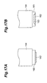
- a flat collet or a pyramidal collet can be used as the collet for suctioning of the chip, and normally when flip-chip bonding is performed, a flat collet is used.
- the CT photodiode array is large in chip area (that is, for example, has a rectangular shape with one side being 20mm in length), and as shown in FIG. 17B, when the pyramidal collet 161 that is normally used in a mounter is used, warping occurs due to the gap 163 that forms between the chip 162 and the pyramidal collet 161 and positional deviation may occur due to this warping and cause lowering of the mounting precision.
- the entire chip surface of the chip 162 contacts the flat collet 160.
- the chip surface that contacts the flat collet 160 is the light-incident surface at which are formed the impurity diffusion layers that make up the photodetecting portion, that is, the photodiode array. If the entirety of this chip surface that is to be the light-incident surface is subject to pressurization and heating while being in contact with the flat collet 160, the photodetecting portion itself receives physical damage. Appearance defects and degradation of characteristics (increased dark current and noise, etc.) due to surface flaws thus occur at the photodetecting portion.
- an object of this invention is to provide a photodiode array, a manufacturing method thereof, and a radiation detector, with which the above issues are resolved and the degradation of characteristics due to damage of the photodiode array in the mounting process can be prevented.
- this invention provides a photodiode array comprising: a semiconductor substrate, wherein a plurality of photodiodes are formed in array form on a surface onto which light to be detected is made incident; and is characterized in that the semiconductor substrate has penetrating wirings, which pass through from the incidence surface side to the back surface side, formed for the photodiodes and a protruding portion, having a predetermined height, is formed at regions of the incidence surface side at which the photodiodes are not formed.
- a protruding portion is disposed at the non-formed regions and this protruding portion functions as a spacer that forms gaps with respect to a flat collet used in a mounting process.
- the photodiodes are thus protected and prevented from directly contacting the flat collet and will thus not receive stress due to pressurization and stress due to heating.
- the above-mentioned protruding portion may be formed of a resin or a metal with a light shielding property. Incidence of light onto the non-formed regions can thereby be prevented and the resolution of the photodiode will be improved.
- the protruding portion comprises a plurality of spacer units and the respective spacer units are formed so as to be positioned intermittently at predetermined intervals.
- the semiconductor substrate has impurity regions (separation layers), which separate the respective photodiodes, disposed between the adjacent photodiodes.
- separation layers impurity regions
- This invention provides a photodiode array manufacturing method comprising: a first step of forming, in a semiconductor substrate, formed of a semiconductor of a first conductive type, penetrating wirings that pass through between the respective surfaces of the semiconductor substrate; a second step of adding an impurity to predetermined regions of a surface at one side of the semiconductor substrate to form a plurality of impurity diffusion layers of a second conductive type and forming a plurality of photodiodes arrayed in array form from the respective impurity diffusion layers and the semiconductor substrate; and a third step of providing on the surface at the one side of the semiconductor substrate, a protruding portion of predetermined height at the non-formed regions at which the photodiodes are not formed.
- a photodiode array having a protruding portion of predetermined height disposed at the non-formed regions of the incidence surface side of the semiconductor substrate, can be manufactured.
- the above-described first step may comprise: a step of forming a plurality of hole portions in the semiconductor substrate; a step of forming a conductive coating film on the surface of at least one side of the semiconductor substrate including the respective hole portions; and a step of polishing the semiconductor substrate to remove the conductive coating film.
- a step, of adding, between adjacent regions to which the impurity is to be added, another impurity to form impurity regions of the first conductive type may be provided.
- a photodiode array wherein adjacent photodiodes are separated securely can be provided.
- this invention provides a radiation detector comprising: any of the above-described photodiode arrays; and a scintillator panel, mounted to the side of the photodiode array onto which the light to be detected is made incident and emits light due to incident radiation.
- This invention also provides a radiation detector, comprising: the photodiode array manufactured by any of the above-described manufacturing methods; and a scintillator panel, mounted to the side of the photodiode array at which the protruding portion is provided and emits light due to incident radiation.
- each of these radiation detectors is equipped with the above-described photodiode array, the photodiodes that are formed on the light-incident surface side are protected by the protruding portion at the non-formed regions and prevented from receiving damage due to pressurization and heating in the mounting process, and degradation of characteristics due to the increase of noise and dark current, etc. by such damage is thus prevented.
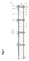
- FIG. 1 is a sectional view showing, in enlarged and schematic manner, the principal portions of a photodiode array of an embodiment.
- FIG. 2 shows a side view of a semiconductor chip that makes up the photodiode array and sectional views showing the principal portions thereof in enlarged manner.
- FIG. 3 is an enlarged sectional view of the principal portions that illustrates an intermediate step in a process of manufacturing the photodiode array of the embodiment.
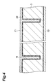
- FIG. 4 is an enlarged sectional view of the principal portions that illustrates a step subsequent that of FIG. 3.
- FIG. 5 is an enlarged sectional view of the principal portions that illustrates a step subsequent that of FIG. 4.
- FIG. 6 is an enlarged sectional view of the principal portions that illustrates a step subsequent that of FIG. 5.
- FIG. 7 is an enlarged sectional view of the principal portions that illustrates a step subsequent that of FIG. 6.
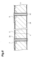
- FIG. 8 is an enlarged sectional view of the principal portions that illustrates a step subsequent that of FIG. 7.
- FIG. 9 is an enlarged sectional view of the principal portions that illustrates a step subsequent that of FIG. 8.
- FIG. 10 is an enlarged sectional view of the principal portions that illustrates a step subsequent that of FIG. 9.
- FIG. 11 is a sectional view showing, in enlarged and schematic manner, the principal portions of another photodiode array of an embodiment.
- FIG. 12 is a sectional view showing, in enlarged and schematic manner, the principal portions of yet another photodiode array of an embodiment.
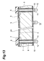
- FIG. 13 is a sectional view showing, in enlarged and schematic manner, the principal portions of yet another photodiode array of an embodiment.
- FIG. 14 is a sectional view showing, in enlarged and schematic manner, the principal portions of a radiation detector having a photodiode array of an embodiment.
- FIG. 15A is a schematic plan view of a photodiode array of an embodiment and illustrates a case where a spacer is formed in a continuous cross-like pattern.
- FIG. 15B is a schematic plan view of a photodiode array of an embodiment and illustrates a case where a spacer is formed in an intermittent pattern.
- FIG. 15C is a schematic plan view of a photodiode array of an embodiment and illustrates a case where a spacer is formed in an intermittent cross-like pattern.
- FIG. 16A is another schematic plan view of a photodiode array of an embodiment and illustrates a case where a spacer is formed in a frame-like pattern.
- FIG. 16B illustrates a case where a frame-like pattern is formed with the frame-like spacer units of FIG. 16A that are partially omitted.
- FIG. 16C illustrates a case where the spacer units of both FIGS. 15A and 16A are provided.
- FIG. 17A is a sectional view schematically showing a state wherein a semiconductor chip is suctioned by a collet and shows a state of suctioning by a flat collet.
- FIG. 17B is a sectional view schematically showing a state wherein a semiconductor chip is suctioned by a collet and shows a state of suctioning by a pyramidal collet.
- FIG. 18 is a sectional view showing a photodiode array of a conventional art.
- FIG. 1 is a sectional view showing, in enlarged and schematic manner, the principal portions of a photodiode array 1 of an embodiment of this invention.
- the surface of incidence of light L shall be called as the front surface and the surface at the opposite side shall be called as the back surface.
- the dimensions are differed as suited for the convenience of illustration.
- Photodiode array 1 has the plurality of photodiodes 4, formed of pn junctions that are arrayed two-dimensionally in a regular array form in the vertical and horizontal directions, and each photodiode 4 functions as a single pixel of photodiode array 1, which, as a whole, makes up a single photodetecting portion.
- the photodiode array 1 has the n-type (first conductive type) silicon substrate 3 with a thickness of approximately 150 to 500 ⁇ m (preferably 400 ⁇ m) and an impurity concentration of approximately 1 ⁇ 10 12 to 10 15 /cm 3 .
- the photodiode array 1 has, on its front surface side, the p-type (second conductive type) impurity diffusion layer 5, with an impurity concentration of approximately 1 ⁇ 10 15 to 10 20 /cm 3 and a film thickness of 0.05 to 20 ⁇ m (preferably 0.2 ⁇ m), arrayed in a regular array form horizontally and vertically.
- the regions at which the respective p-type impurity diffusion layers 5 exist are the regions at which the photodiodes 4 are formed (formed regions), the regions besides these are non-formed regions where photodiodes are not formed, and at the non-formed regions of the front surface side is disposed a spacer 6, which is a protruding portion having a predetermined pattern.
- This spacer 6 is formed of a resin, metal, or insulating material and protrudes to a predetermined height (in the present embodiment, this height is set to a suitable height (thickness) from the front surface n-type silicon substrate 3 that is greater than the film thickness of the electrode wirings 9 to be described later).
- the photodiode array 1 also has the penetrating wiring 8 provided for each photodiode 4.
- Each penetrating wiring 8 passes through from the front surface side to the back surface side of the n-type silicon substrate 3, is formed to a diameter of approximately 10 ⁇ m to 100 ⁇ m (preferably approximately 50 ⁇ m), is formed of polysilicon with a phosphorus concentration of approximately 1 ⁇ 10 15 to 10 20 /cm 3 , has its front surface side electrically connected to the p-type impurity diffusion layer 5 via the electrode wiring 9 (with a film thickness of approximately 1 ⁇ m) formed of aluminum, and has its back surface side electrically connected to the electrode pad 10 (with a film thickness of 0.05 ⁇ m to 5 ⁇ m and preferably approximately 1 ⁇ m) formed likewise of aluminum.
- each penetrating wiring 8 is disposed in a non-formed region at which the photodiode 4 is not formed, it may be disposed in another portion instead.
- the illustrated photodiode array 1 furthermore has n + -type impurity regions (separation layers) 7 provided to a depth of approximately 0.5 to 6 ⁇ m between the p-type impurity diffusion layers 5, that is, between the adjacent photodiodes 4.
- This n + -type impurity region (separation layer) 7 has a function of electrically separating the adjacent photodiodes 4, and thus by the provision thereof, the adjacent photodiodes 4 are electrically separated securely and crosstalk among the photodiodes 4 can be reduced.
- the photodiode array 1 has photodetecting characteristics that are adequately allowable in terms of practical use.
- FIG. 2 shows a side view of the semiconductor chip 30 that makes up the photodiode array 1 and sectional views showing the principal portions thereof in enlarged manner.
- the semiconductor chip 30 has an extremely thin, plate-like form with a width W1 of approximately 22.4mm and a thickness D of approximately 0.3mm, has a plurality of the above-described photodiodes 4 (for example, has a two-dimensional array of 16 ⁇ 16 photodiodes), and is a large area (for example, approximately 22.4mm ⁇ 22.4mm) chip wherein pitch W2 between adjacent pixels is approximately 1.4mm.
- the photodiode array 1 With the photodiode array 1 arranged as described above, when light L is made incident from the front surface side, this light L to be detected is made incident on the respective p-type impurity diffusion layers 5, and carriers corresponding to the incident light are generated by the respective photodiodes 4.
- the photocurrents due to the generated carriers are taken out from the bump electrodes 12 via the electrode wirings 9 and the penetrating wirings 8, connected to the respective p-type impurity diffusion layers 5 and furthermore via the respective electrodes pads 10 and the UBMs 11 at the back surface side.
- the incident light is detected by these outputs from the bump electrodes 12.
- the photodiode array 1 has spacer 6 provided at the non-formed regions.
- this spacer 6 contacts the flat collet and functions to secure gaps between the formed regions of the photodiodes 4, which make up the photodetecting portion, and the flat collet.
- the formed regions are thus protected by the spacer 6 and will not contact the flat collet directly.
- the photodiode array 1 since the photodetecting portion thus does not directly receive stress due to pressurization or stress due to heating, the photodetecting portion itself will not receive physical damage and the generation of noise and dark current due to such damage can be restrained.
- the photodiode array 1 can thus perform photodetection of high precision (high S/N ratio).
- the spacer 6 contacts the flat collet directly and is pressurized and heated when flip-chip bonding is performed, it is preferably provided using a material that can exhibit a protective function that enables protection of the respective photodiodes 4 from the pressurization and the heating.
- the spacer 6 when the spacer 6 is formed of resin, in consideration of the thermal expansion coefficient, flexibility, elastic characteristics, and conditions such as impurity ions not diffusing into the respective photodiodes 4 due to heating, etc. an epoxy resin, a polyimide resin, a silicone resin, a urethane resin, an acrylic resin, a fluorine resin, or a composite material having these resins as base materials is used and the film thickness is set to 2 to 30 ⁇ m (preferably 5 to 6 ⁇ m).
- the spacer 6 is provided using such a resin, the surface protection effect in the process of mounting the photodiode array 1 will be high. Moreover, the spacer 6 will not affect the electrical characteristics of the photodiodes 4 and the manufacturing method will be simple.
- a polyimide resin is especially favorable in having good heat resistance and not degrading due to the heat that can be received from the flat collet in the mounting process.
- a light shielding property may also be provided to the resin of the spacer 6 by the addition of a filler.
- the spacer 6 may be formed of metal, and in this case, a metal with a light shielding property is preferable.
- a metal with a light shielding property For example, Al (aluminum), Au (gold), Ni (nickel), Cr (chromium), Ti, or a silicide-based metal, etc. can be used and such metals may be laminated together.
- the film thickness of the former is set to approximately 1 ⁇ m and the film thickness of the latter is set to approximately 5 ⁇ m. If in the case where the spacer 6 is to be formed of metal, the electrode wirings 9 exist at a layer below the spacer 6, shorting among photodiodes may occur and cause a problem, a film having an insulating property is disposed between the spacer 6 and the electrode wirings 9.
- an insulating material can be used for the spacer 6, and in this case, glass (SiO 2 ), SiN, low melting point glass, etc. can be used.
- FIGS. 15A to C and 16A to C are schematic planar views of the photodiode array 1 as viewed from the light-incident surface.
- the spacer 6 may be formed in a continuous cross-like pattern 6a by positioning a plurality of long, continuous, wall-like spacer units 13a in a regular manner in the vertical and horizontal directions and intersecting these in cross-like form.
- an intermittent pattern 6b may be formed by intermittently positioning a plurality of short, wall-like spacer units 13c at predetermined intervals at portions besides corner portions 13b of the non-formed regions, or as shown in FIG. 15C, an intermittent cross-like pattern 6c may be obtained by positioning a plurality of cross-like spacer units 13d at the respective corner portions 13b.
- planar patterns are all regular patterns that can be obtained by positioning a plurality of spacer units in a regular manner
- an irregular pattern may be formed instead by setting the mutual positioning intervals of the short, wall-like spacer units 13c or the cross-like spacer units 13d in an irregular manner.
- the spacer 6 is provided in a planar pattern such as those described above, a plurality of pixel regions 17, which are partitioned by the spacer 6, are formed at the front surface side, the adjacent pixel regions 17 are preferably in communication with each other and not partitioned completely by the spacer 6.
- the spacer 6 is, for example, provided in a planar pattern in which the spacer units are positioned intermittently as in the above-described intermittent pattern 6b or the intermittent cross-like pattern 6c.
- the spacer 6 may be formed, for example, in a frame-like pattern 6d by positioning a rimmed frame-like spacer units 13e at positions by which the entire formed regions of the photodiodes 4 can be surrounded and the pixel regions 17 may be disposed in the interior as shown in FIG. 16A.
- frame-like spacer units 13f with omitted portions may be provided to form a frame-like pattern 6e as shown in FIG. 16B.
- the pixel regions 17 are formed without being partitioned from each other by the spacer 6.
- the gaps between the adjacent spacer units function as relief paths for resin (for example, an optical resin 35 that is used to adhere a scintillator panel 31 to form a radiation detector 40 as shall be described later).
- resin for example, an optical resin 35 that is used to adhere a scintillator panel 31 to form a radiation detector 40 as shall be described later.
- the spacer 6 may be provided in a planar pattern having both the wall-like spacer units 13a and the frame-like spacer units 13e as shown in FIG. 16C, in this case, the respective pixel regions 17 are partitioned by the spacer 6. In this case, if the spacer 6 with a light shielding property is applied, since all of the pixel regions 17 will be partitioned uniformly by the spacer 6, the structure that is formed can be said to be suitable for improving the resolution of the photodiode array.
- the above-described photodiode array 1 may also be arranged as follows. That is, for example as shown in FIG. 11, phosphorus may be diffused in side walls of the pore portions 15 to provide the n + -type impurity regions 7 at the surroundings of the penetrating wirings 8 as well. Unnecessary carriers from damaged layers formed in the process of forming the pore portions 15 (hole portions 14) can thereby be trapped to restrain the dark current.
- the concentration of phosphorus to be added in this case is set to approximately 1 ⁇ 10 15 to 10 20 /cm 3 and the thickness (depth) of each n + -type impurity region 7 is set to approximately 0.1 to 5 ⁇ m.
- a silicon nitride film 26 with a film thickness of approximately 0.1 to 2 ⁇ m may be disposed on a silicon oxide film 20 inside each pore portion 15 as shown in FIG. 12. By doing so, the insulation between n-type silicon substrate 3 and penetrating wirings 8 can be secured to reduce operation faults.
- the n + -type impurity regions 7 may also be provided at the back surface side by doping and diffusing phosphorus as shown in FIG. 13.
- cathode electrodes 16 can be led out from the back surface.
- electrodes to serve as cathodes may also be disposed at the back surface side upon providing penetrating wirings from the n + -type impurity regions 7 formed on the front surface.
- FIGS. 3 to 10 A method of manufacturing the present embodiment's photodiode array I shall now be described with reference to FIGS. 3 to 10.
- the n-type silicon substrate 3 with a thickness of approximately 150 to 500 ⁇ m (preferably 400 ⁇ m) is prepared. Then as shown in FIG.
- the penetrating wiring 8 is formed in a later step.
- the silicon oxide film (SiO 2 ) 20 realizes the electrical insulation between the penetrating wirings 8 to be described later and n-type silicon substrate 3.
- the hole portions 14 are filled by polysilicon that has been made low in resistance by the addition of the impurity.
- the front surface and the back surface or just the front surface of the substrate are polished to remove the polysilicon film 21 that had been formed on the front surface and the back surface or just the front surface and expose the polysilicon embedded in the hole portions 14 at the front surface and the back surface and thereby form pore portions 15 passing through between the surfaces at both sides and make the embedded polysilicon become the penetrating wirings 8.
- the front surface and the back surface of the substrate are then thermally oxidized again to form a silicon oxide films 22. These silicon oxide films 22 are used as n + thermal diffusion masks in a subsequent step.
- the silicon oxide film 22 at the front surface side of the n-type silicon substrate 3 is then patterned using a predetermined photomask to open just the regions at which the n + -type impurity regions 7 are to be provided, and phosphorus is diffused from the opened portions (open portions) to provide the n + -type impurity regions 7 (in the case where the n + -type impurity regions 7 are not to be provided this step (impurity region forming step) may be omitted).
- the front surface and the back surface of the substrate are thermally oxidized again to form the silicon oxide films 23 (see FIG. 6). These silicon oxide films 23 are used as masks in the process of forming the p-type impurity diffusion layers 5.
- Patterning using a predetermined photomask is then performed on the silicon oxide film 23 and just the regions at which the p-type impurity diffusion layers 5 are to be formed are opened. Boron is then diffused from the opened portions and the p-type impurity diffusion layers 5 are formed so as to be arrayed vertically and horizontally in a two-dimensional array. Thereafter, the front surface and the back surface of the substrate are thermally oxidized again to form silicon oxide films 24 (see FIG. 7).
- the photodiodes 4, formed by the pn junctions of the respective p-type impurity diffusion layers 5 and the n-type silicon substrate 3 are thus formed so as to be arrayed vertically and horizontally in a two-dimensional array and these photodiodes 4 become portions corresponding to pixels.
- Electrodes are then formed at the regions at which the respective penetrating wirings 8 are formed. Subsequently, upon forming aluminum metal films over the entire front surface and back surface, patterning is performed using a predetermined photomask and unnecessary portions of the metal film are removed to form the electrode wirings 9 at the front surface side and the electrode pads 10 at the back surface side (see FIG. 8). In the FIGURE, just the anode electrode lead-out portions are shown. Though not illustrated, to lead out cathode electrodes from a surface, electrodes can be lead out from the n + -type impurity regions 7 to the back surface via the electrode wirings 9 and penetrating wirings 8.
- the spacer 6 is then formed on the front surface side of the n-type silicon substrate 3 (see FIG. 9).
- the spacer 6 is to be formed of resin
- the resin which is to be the material of the spacer
- the resin is coated onto the front surface side, spread over the entire surface by spin coating or screen printing, and then cured.
- a photosensitive resin photoresist
- a predetermined photomask is used to form a resist pattern corresponding to the spacer 6 that is to be formed by exposure and development, and using this mask, the spacer resin is made to remain just at predetermined regions to thereby form the spacer 6 of the predetermined pattern.
- the spacer in the case where the resin of spacer 6 is photosensitive, the spacer can be obtained directly using a predetermined photomask to perform exposure and development and then performing curing in a suitable manner.
- the formed regions of the photodiodes 4 that make up the photodetecting portion are prevented from contacting a flat collet in the mounting process and are thus protected.
- the spacer 6 is to be formed of a metal
- a coating film of the metal that is to be the material of the spacer 6 is formed by vapor deposition, sputtering, CVD, or other method
- a resist pattern is then formed by the above-described procedure, and using this pattern as a mask, the coating film is made to remain just at predetermined regions to form the spacer 6 of the predetermined pattern.
- the film thickness of the coating film may be made thick by plating.
- a suitable insulating film is formed between the spacer 6 and the electrode wiring 9, etc.
- the insulating film is preferably one with good light transmitting characteristics, and may be a film of SiO 2 , SiN, etc. that is formed by vapor deposition, sputtering, or CVD, or a film of a resin, such as a polyimide or an acrylate, and the film may be formed over the entire front surface of the photodiode array 1 or may be patterned so as to remain just at the necessary locations.
- the bump electrodes 12 are then provided at the respective electrode pads 10, and in the case where solder is to be used as the bump electrodes 12, since solder is poor in wettability with respect to aluminum, the UBMs 11 for intervening between the respective electrode pads 10 and bump electrodes 12 are formed on the respective electrode pads 10 and bump electrodes 12 are formed overlappingly on UBMs 11(see FIG. 10).
- the UBMs 11 are formed by electroless plating and using Ni-Au, the UBMs may be formed instead by the lift-off method and using Ti-Pt-Au or Cr-Au.
- plating must be performed upon protecting the front surface and back surface by a insulating film so that just the portions at which the UBMs 11 are to be formed, that is, just the respective electrode pads 10 will be exposed.
- the bump electrodes 12 are obtained by forming solder on predetermined the UBMs 11 by a solder ball mounting method or printing method and performing reflow.
- the bump electrodes 12 are not limited to those formed of solder and may be gold bumps, nickel bumps, or copper bumps or even conductive resin bumps, which contain a conductive filler or other metal.
- FIG. 14 is sectional side view of the radiation detector 40 of the embodiment.
- This radiation detector 40 has the scintillator panel 31, onto which radiation is made incident and which emits light, generated as a result of the radiation, from a light emitting surface 31a, and the above-described photodiode array 1, onto which the light emitted from the scintillator panel 31 is made incident and which converts the light to electrical signals.
- This radiation detector 40 is characterized in having this invention's photodiode array 1.
- the scintillator panel 31 is mounted to the front surface side (incidence surface side) of the photodiode array 1, and the photodiode array 1 has the above-described spacer 6 disposed at its front surface side. Though the back surface of scintillator 31, that is, a light emitting surface 31a will thus contact the spacer 6, it will not contact the formed regions of the photodiodes 4 directly.
- an optical resin 35 having a refractive index such that will prevent the degradation of the light transmitting characteristics, is filled in these gaps, and by this optical resin 35, the light emitted from the scintillator panel 31 is made incident on the photodiode array 1 efficiently.
- an epoxy resin, acrylic resin, urethane resin, silicone resin, fluorine resin, etc. having the property of transmitting the light emitted from the scintillator panel 31, may be used or a composite material having these resins as the base material may be used.
- the front surface is suctioned by a flat collet.
- the suctioning surface of the flat collet will not contact the photodetecting portion directly, and direct contacting of the light emitting surface 31 a with the formed regions of the photodiodes 4 due to the mounting of the scintillator 31 will also not occur. Since with the radiation detector 40, having such the photodiode array 1 and the scintillator panel 31, the generation of noise, dark current, etc. due to the damaging of the photodetecting portion in the mounting process can be prevented, photodetection can be performed with high precision and the detection of radiation can also be performed at high precision.
- the generation of noise, dark current, etc. due to the damaging of the photodetecting portion in the mounting process can be prevented effectively in a photodiode array, a method of manufacturing the same, and a radiation detector.
Landscapes
- Measurement Of Radiation (AREA)
- Solid State Image Pick-Up Elements (AREA)
- Light Receiving Elements (AREA)
Abstract
Description
Claims (9)
- A photodiode array comprising:characterized in that the semiconductor substrate has penetrating wirings, which pass through from the incidence surface side to the back surface side, formed for the photodiodes anda semiconductor substrate, wherein a plurality of photodiodes are formed in array form on a surface onto which light to be detected is made incident; and
a protruding portion, having a predetermined height, is formed at regions of the incidence surface side at which the photodiodes are not formed. - The photodiode array according to Claim 1, wherein
the protruding portion is formed of a resin or a metal with a light shielding property. - The photodiode array according to Claim 1 or 2, wherein
the protruding portion comprises a plurality of spacer units and the respective spacer units are formed so as to be positioned intermittently at predetermined intervals. - The photodiode array according to any of Claims 1 through 3, wherein the semiconductor substrate has impurity regions, which separate the respective photodiodes, disposed between the adjacent photodiodes.
- A photodiode array manufacturing method comprising:a first step of forming, in a semiconductor substrate, formed of a semiconductor of a first conductive type, penetrating wirings that pass through between the respective surfaces of the semiconductor substrate;a second step of adding an impurity to predetermined regions of a surface at one side of the semiconductor substrate to form a plurality of impurity diffusion layers of a second conductive type and forming a plurality of photodiodes arrayed in array form from the respective impurity diffusion layers and the semiconductor substrate; anda third step of providing on the surface at one side of the semiconductor substrate, a protruding portion of predetermined height at the non-formed regions at which the photodiodes are not formed.
- The photodiode array manufacturing method according to Claim 5, wherein
the first step comprises: a step of forming a plurality of hole portions in the semiconductor substrate; a step of forming a conductive coating film on the surface of at least one side of the semiconductor substrate including the respective hole portions; and a step of polishing the semiconductor substrate to remove the conductive coating film. - The photodiode array manufacturing method according to Claim 5 or 6, wherein subsequent the first step is provided a step, of adding, between adjacent regions to which the impurity is to be added, another impurity to form impurity regions of the first conductive type.
- A radiation detector comprising:the photodiode array according to any of Claims 1 through 4; and a scintillator panel, mounted to the side of the photodiode array onto which the light to be detected is made incident and emits light due to incident radiation.
- A radiation detector, comprising:the photodiode array manufactured by the manufacturing method according to any of Claims 5 through 7; anda scintillator panel, mounted to the side of the photodiode array at which the protruding portion is provided and emits light due to incident radiation.
Applications Claiming Priority (3)
| Application Number | Priority Date | Filing Date | Title |
|---|---|---|---|
| JP2003063904 | 2003-03-10 | ||
| JP2003063904 | 2003-03-10 | ||
| PCT/JP2004/003090 WO2004082023A1 (en) | 2003-03-10 | 2004-03-10 | Photodiode array, method for manufacturing same, and radiation detector |
Publications (3)
| Publication Number | Publication Date |
|---|---|
| EP1605513A1 true EP1605513A1 (en) | 2005-12-14 |
| EP1605513A4 EP1605513A4 (en) | 2008-04-09 |
| EP1605513B1 EP1605513B1 (en) | 2015-01-07 |
Family
ID=32984451
Family Applications (1)
| Application Number | Title | Priority Date | Filing Date |
|---|---|---|---|
| EP04719058.2A Expired - Lifetime EP1605513B1 (en) | 2003-03-10 | 2004-03-10 | Photodiode array, method for manufacturing same, and radiation detector |
Country Status (8)
| Country | Link |
|---|---|
| US (1) | US7696620B2 (en) |
| EP (1) | EP1605513B1 (en) |
| JP (1) | JP4224060B2 (en) |
| KR (1) | KR101029178B1 (en) |
| CN (2) | CN101373783B (en) |
| IL (1) | IL170733A (en) |
| TW (1) | TWI324399B (en) |
| WO (1) | WO2004082023A1 (en) |
Families Citing this family (18)
| Publication number | Priority date | Publication date | Assignee | Title |
|---|---|---|---|---|
| JP4247017B2 (en) * | 2003-03-10 | 2009-04-02 | 浜松ホトニクス株式会社 | Manufacturing method of radiation detector |
| JP2008071882A (en) * | 2006-09-13 | 2008-03-27 | Hamamatsu Photonics Kk | Photodetector |
| JPWO2009139209A1 (en) * | 2008-05-12 | 2011-09-15 | コニカミノルタエムジー株式会社 | Radiation image detector and method for manufacturing radiation image detector |
| JP5205241B2 (en) | 2008-05-15 | 2013-06-05 | 浜松ホトニクス株式会社 | Spectroscopic module |
| JP5207938B2 (en) | 2008-05-15 | 2013-06-12 | 浜松ホトニクス株式会社 | Spectroscopic module and method for manufacturing spectral module |
| JP5205238B2 (en) * | 2008-05-15 | 2013-06-05 | 浜松ホトニクス株式会社 | Spectroscopic module |
| JP2009300418A (en) * | 2008-05-15 | 2009-12-24 | Hamamatsu Photonics Kk | Spectroscopic module |
| JP5205240B2 (en) * | 2008-05-15 | 2013-06-05 | 浜松ホトニクス株式会社 | Spectroscopic module manufacturing method and spectroscopic module |
| JP5415060B2 (en) | 2008-05-15 | 2014-02-12 | 浜松ホトニクス株式会社 | Spectroscopic module |
| US8405115B2 (en) * | 2009-01-28 | 2013-03-26 | Maxim Integrated Products, Inc. | Light sensor using wafer-level packaging |
| JP5610520B2 (en) * | 2010-07-07 | 2014-10-22 | 日本結晶光学株式会社 | Radiation detector |
| JP5756803B2 (en) * | 2010-07-23 | 2015-07-29 | シャープ株式会社 | Light emitting device and manufacturing method thereof |
| US8569704B2 (en) * | 2010-12-21 | 2013-10-29 | Carestream Health, Inc. | Digital radiographic detector array including spacers and methods for same |
| US8558185B2 (en) * | 2010-12-21 | 2013-10-15 | Carestream Health, Inc. | Digital radiographic detector array including spacers and methods for same |
| JP6018372B2 (en) * | 2011-09-22 | 2016-11-02 | 野洲メディカルイメージングテクノロジー株式会社 | Radiation image sensor and photoelectric conversion element array unit |
| JP5941713B2 (en) * | 2012-03-14 | 2016-06-29 | 東京エレクトロン株式会社 | Wafer inspection interface and wafer inspection apparatus |
| WO2019123591A1 (en) * | 2017-12-21 | 2019-06-27 | オリンパス株式会社 | Semiconductor device |
| WO2023092333A1 (en) * | 2021-11-24 | 2023-06-01 | Shanghai United Imaging Healthcare Co., Ltd. | Detector systems for imaging |
Family Cites Families (17)
| Publication number | Priority date | Publication date | Assignee | Title |
|---|---|---|---|---|
| JPS5985188A (en) * | 1982-11-08 | 1984-05-17 | Nec Corp | Solid-state image pickup device |
| NL8700370A (en) * | 1987-02-16 | 1988-09-16 | Philips Nv | RADIATION-SENSITIVE SEMICONDUCTOR DEVICE. |
| JPH073918B2 (en) * | 1988-05-17 | 1995-01-18 | 清水建設株式会社 | Open-type electromagnetic shielding window |
| JP3168811B2 (en) | 1994-03-23 | 2001-05-21 | 富士電機株式会社 | Thin film photoelectric conversion device and method of manufacturing the same |
| JP3197512B2 (en) * | 1997-07-25 | 2001-08-13 | アロカ株式会社 | Semiconductor radiation detector |
| JPH11126892A (en) * | 1997-10-24 | 1999-05-11 | Matsushita Electron Corp | Solid-state imaging device and method of manufacturing the same |
| US6169317B1 (en) * | 1998-02-13 | 2001-01-02 | Canon Kabushiki Kaisha | Photoelectric conversion device and image sensor |
| JP3586128B2 (en) * | 1998-02-13 | 2004-11-10 | キヤノン株式会社 | Photoelectric conversion element and image sensor |
| JP3792445B2 (en) * | 1999-03-30 | 2006-07-05 | 日本特殊陶業株式会社 | Wiring board with capacitor |
| JP2001318155A (en) | 2000-02-28 | 2001-11-16 | Toshiba Corp | Radiation detector and X-ray CT device |
| US6566685B2 (en) * | 2000-04-12 | 2003-05-20 | Casio Computer Co., Ltd. | Double gate photo sensor array |
| JP2002270808A (en) * | 2001-03-13 | 2002-09-20 | Matsushita Electric Ind Co Ltd | MOS type imaging device |
| JP2003084066A (en) * | 2001-04-11 | 2003-03-19 | Nippon Kessho Kogaku Kk | Radiation detector parts, radiation detectors and radiation detectors |
| JP4653336B2 (en) * | 2001-04-18 | 2011-03-16 | 浜松ホトニクス株式会社 | Energy ray detector and apparatus |
| JP3735547B2 (en) | 2001-08-29 | 2006-01-18 | 株式会社東芝 | Semiconductor device and manufacturing method thereof |
| JP2003066150A (en) * | 2001-08-30 | 2003-03-05 | Canon Inc | Fluorescent plate, radiation detection device and radiation detection system |
| JP2003197854A (en) * | 2001-12-26 | 2003-07-11 | Nec Electronics Corp | Double-sided connection type semiconductor device, multistage stacked type semiconductor device, method for manufacturing the same, and electronic component equipped with the semiconductor device |
-
2004
- 2004-03-10 EP EP04719058.2A patent/EP1605513B1/en not_active Expired - Lifetime
- 2004-03-10 TW TW093106303A patent/TWI324399B/en not_active IP Right Cessation
- 2004-03-10 CN CN200810169538XA patent/CN101373783B/en not_active Expired - Lifetime
- 2004-03-10 KR KR1020057016790A patent/KR101029178B1/en not_active Expired - Fee Related
- 2004-03-10 JP JP2005503542A patent/JP4224060B2/en not_active Expired - Lifetime
- 2004-03-10 US US10/548,413 patent/US7696620B2/en not_active Expired - Lifetime
- 2004-03-10 CN CNB2004800067487A patent/CN100438054C/en not_active Expired - Lifetime
- 2004-03-10 WO PCT/JP2004/003090 patent/WO2004082023A1/en not_active Ceased
-
2005
- 2005-09-07 IL IL170733A patent/IL170733A/en active IP Right Grant
Also Published As
| Publication number | Publication date |
|---|---|
| CN101373783B (en) | 2010-06-23 |
| CN1759486A (en) | 2006-04-12 |
| TW200501439A (en) | 2005-01-01 |
| EP1605513A4 (en) | 2008-04-09 |
| US7696620B2 (en) | 2010-04-13 |
| IL170733A (en) | 2011-03-31 |
| TWI324399B (en) | 2010-05-01 |
| WO2004082023A1 (en) | 2004-09-23 |
| CN100438054C (en) | 2008-11-26 |
| JP4224060B2 (en) | 2009-02-12 |
| CN101373783A (en) | 2009-02-25 |
| EP1605513B1 (en) | 2015-01-07 |
| US20070090477A1 (en) | 2007-04-26 |
| KR101029178B1 (en) | 2011-04-12 |
| KR20050115899A (en) | 2005-12-08 |
| JPWO2004082023A1 (en) | 2006-06-15 |
Similar Documents
| Publication | Publication Date | Title |
|---|---|---|
| US8389322B2 (en) | Photodiode array, method of manufacturing the same, and radiation detector | |
| EP1605513B1 (en) | Photodiode array, method for manufacturing same, and radiation detector | |
| EP1605514A1 (en) | Photodiode array, method for manufacturing same, and radiation detector | |
| JP4220817B2 (en) | Photodiode array, method of manufacturing the same, and radiation detector | |
| EP1608020A1 (en) | Photodiode array and production method thereof, and radiation detector | |
| JP4808748B2 (en) | Manufacturing method of photodiode array | |
| US7663169B2 (en) | Photodiode array and production method thereof, and radiation detector | |
| JP4808760B2 (en) | Manufacturing method of radiation detector | |
| JP4808759B2 (en) | Radiation detector |
Legal Events
| Date | Code | Title | Description |
|---|---|---|---|
| PUAI | Public reference made under article 153(3) epc to a published international application that has entered the european phase |
Free format text: ORIGINAL CODE: 0009012 |
|
| 17P | Request for examination filed |
Effective date: 20050926 |
|
| AK | Designated contracting states |
Kind code of ref document: A1 Designated state(s): AT BE BG CH CY CZ DE DK EE ES FI FR GB GR HU IE IT LI LU MC NL PL PT RO SE SI SK TR |
|
| AX | Request for extension of the european patent |
Extension state: AL LT LV MK |
|
| DAX | Request for extension of the european patent (deleted) | ||
| RBV | Designated contracting states (corrected) |
Designated state(s): DE FR GB NL |
|
| A4 | Supplementary search report drawn up and despatched |
Effective date: 20080311 |
|
| 17Q | First examination report despatched |
Effective date: 20101020 |
|
| GRAP | Despatch of communication of intention to grant a patent |
Free format text: ORIGINAL CODE: EPIDOSNIGR1 |
|
| RIC1 | Information provided on ipc code assigned before grant |
Ipc: H01L 31/10 20060101ALI20140717BHEP Ipc: H01L 27/144 20060101ALI20140717BHEP Ipc: H01L 31/0232 20140101ALI20140717BHEP Ipc: G01T 1/20 20060101ALI20140717BHEP Ipc: H01L 27/146 20060101AFI20140717BHEP Ipc: H01L 23/12 20060101ALI20140717BHEP |
|
| INTG | Intention to grant announced |
Effective date: 20140731 |
|
| GRAS | Grant fee paid |
Free format text: ORIGINAL CODE: EPIDOSNIGR3 |
|
| GRAA | (expected) grant |
Free format text: ORIGINAL CODE: 0009210 |
|
| AK | Designated contracting states |
Kind code of ref document: B1 Designated state(s): DE FR GB NL |
|
| REG | Reference to a national code |
Ref country code: GB Ref legal event code: FG4D |
|
| REG | Reference to a national code |
Ref country code: NL Ref legal event code: T3 |
|
| REG | Reference to a national code |
Ref country code: DE Ref legal event code: R096 Ref document number: 602004046459 Country of ref document: DE Effective date: 20150226 |
|
| REG | Reference to a national code |
Ref country code: DE Ref legal event code: R097 Ref document number: 602004046459 Country of ref document: DE |
|
| PLBE | No opposition filed within time limit |
Free format text: ORIGINAL CODE: 0009261 |
|
| STAA | Information on the status of an ep patent application or granted ep patent |
Free format text: STATUS: NO OPPOSITION FILED WITHIN TIME LIMIT |
|
| 26N | No opposition filed |
Effective date: 20151008 |
|
| REG | Reference to a national code |
Ref country code: FR Ref legal event code: PLFP Year of fee payment: 13 |
|
| PGFP | Annual fee paid to national office [announced via postgrant information from national office to epo] |
Ref country code: NL Payment date: 20160210 Year of fee payment: 13 Ref country code: FR Payment date: 20160208 Year of fee payment: 13 Ref country code: GB Payment date: 20160309 Year of fee payment: 13 |
|
| REG | Reference to a national code |
Ref country code: NL Ref legal event code: MM Effective date: 20170401 |
|
| GBPC | Gb: european patent ceased through non-payment of renewal fee |
Effective date: 20170310 |
|
| REG | Reference to a national code |
Ref country code: FR Ref legal event code: ST Effective date: 20171130 |
|
| PG25 | Lapsed in a contracting state [announced via postgrant information from national office to epo] |
Ref country code: NL Free format text: LAPSE BECAUSE OF NON-PAYMENT OF DUE FEES Effective date: 20170401 Ref country code: FR Free format text: LAPSE BECAUSE OF NON-PAYMENT OF DUE FEES Effective date: 20170331 |
|
| PG25 | Lapsed in a contracting state [announced via postgrant information from national office to epo] |
Ref country code: GB Free format text: LAPSE BECAUSE OF NON-PAYMENT OF DUE FEES Effective date: 20170310 |
|
| PGFP | Annual fee paid to national office [announced via postgrant information from national office to epo] |
Ref country code: DE Payment date: 20180227 Year of fee payment: 15 |
|
| REG | Reference to a national code |
Ref country code: DE Ref legal event code: R119 Ref document number: 602004046459 Country of ref document: DE |
|
| PG25 | Lapsed in a contracting state [announced via postgrant information from national office to epo] |
Ref country code: DE Free format text: LAPSE BECAUSE OF NON-PAYMENT OF DUE FEES Effective date: 20191001 |