EP1603381B1 - Federblech in einem Gehäuse als Abschirmung für ein elektronisches hochfrequenztechnisches Gerät - Google Patents
Federblech in einem Gehäuse als Abschirmung für ein elektronisches hochfrequenztechnisches Gerät Download PDFInfo
- Publication number
- EP1603381B1 EP1603381B1 EP05013745A EP05013745A EP1603381B1 EP 1603381 B1 EP1603381 B1 EP 1603381B1 EP 05013745 A EP05013745 A EP 05013745A EP 05013745 A EP05013745 A EP 05013745A EP 1603381 B1 EP1603381 B1 EP 1603381B1
- Authority
- EP
- European Patent Office
- Prior art keywords
- shielding
- circuit board
- housing
- latching
- shield
- Prior art date
- Legal status (The legal status is an assumption and is not a legal conclusion. Google has not performed a legal analysis and makes no representation as to the accuracy of the status listed.)
- Expired - Lifetime
Links
Images


Classifications
-
- H—ELECTRICITY
- H05—ELECTRIC TECHNIQUES NOT OTHERWISE PROVIDED FOR
- H05K—PRINTED CIRCUITS; CASINGS OR CONSTRUCTIONAL DETAILS OF ELECTRIC APPARATUS; MANUFACTURE OF ASSEMBLAGES OF ELECTRICAL COMPONENTS
- H05K9/00—Screening of apparatus or components against electric or magnetic fields
- H05K9/0007—Casings
- H05K9/002—Casings with localised screening
- H05K9/0022—Casings with localised screening of components mounted on printed circuit boards [PCB]
- H05K9/0024—Shield cases mounted on a PCB, e.g. cans or caps or conformal shields
- H05K9/0026—Shield cases mounted on a PCB, e.g. cans or caps or conformal shields integrally formed from metal sheet
- H05K9/0028—Shield cases mounted on a PCB, e.g. cans or caps or conformal shields integrally formed from metal sheet with retainers or specific soldering features
-
- H—ELECTRICITY
- H05—ELECTRIC TECHNIQUES NOT OTHERWISE PROVIDED FOR
- H05K—PRINTED CIRCUITS; CASINGS OR CONSTRUCTIONAL DETAILS OF ELECTRIC APPARATUS; MANUFACTURE OF ASSEMBLAGES OF ELECTRICAL COMPONENTS
- H05K3/00—Apparatus or processes for manufacturing printed circuits
- H05K3/30—Assembling printed circuits with electric components, e.g. with resistors
- H05K3/306—Assembling printed circuits with electric components, e.g. with resistors with lead-in-hole components
- H05K3/308—Adaptations of leads
Definitions
- the invention relates to an electronic high-frequency technical device with a housing made of an electrically conductive material according to the features of the preamble of patent claim 1.
- At least one electronic module in particular a plurality of submodules, is accommodated in this housing of the electronic device for realizing the function of the electronic device.
- These sub-modules can be arranged on a common printed circuit board (motherboard). This arrangement can be made for example via connectors, so that the sub-modules, which in turn consist of printed circuit boards with electronic components, are plugged onto the motherboard. Due to the application of the electronic device in the high frequency range, it is necessary to shield the individual modules with each other to avoid interference in their function and mutual interference. For this purpose, it has already been proposed to separate the individual modules from each other by means of shielding plates in terms of high frequency from one another or to surround them with a shielding housing.
- an electronic high-frequency technical device having a housing made of an electrically conductive material, wherein in the housing at least one electronic module and an associated Ableteil is arranged and further comprising the Ableasable attachment to a printed circuit board arranged in the housing.
- the means for releasably securing are formed as a tab with a hole in the shielding, which is fastened with a screw connection to the circuit board.
- a shielding part with locking means is known in which the shielding part has a latching hook, which is performed by a recess in a printed circuit board and engages behind the underside of the printed circuit board.
- the invention is therefore an object of the invention to provide an electronic device with a housing for high-frequency applications, in which the shielding of modules or sub-modules is improved within the housing to reduce mutual interference significantly, and given in the simple assembly and disassembly steps are.
- the means are designed as latching means and the latching means is designed to be resilient so that the shielding is biased after fixing to the circuit board.
- the releasable attachment is in a particularly advantageous manner a latching connection, to which the shielding part has a latching nose with an arcuate projection, which is inserted into a corresponding recess in the circuit board and locked after the complete plugging.
- the latching means in particular the latching lug and the corresponding recess in the circuit board are equipped so that after locking the shielding is reliably and durably secured to the circuit board, but in the case of disassembly for the purpose of replacing the electronic module can be easily solved.
- the circuit board has a projection and the shielding is provided with a corresponding recess, is conceivable, but not preferred due to the more complex construction.
- the shielding, as well as the means for electrical contact between the housing and the shielding consist of an electrically conductive sheet material and processed by means of a punching process for the purpose of shaping.
- the shielding (shield or shielding or the like) can be punched out of a sheet, optionally formed, wherein at this same time the locking means are formed with this punching.
- the latching lug is formed as a tab-shaped element which has a bow-shaped projection. With this projection, the locking lug is reliably fixed to the circuit board.
- FIG. 1 concerns, as far as shown in detail, a housing of an electronic device for high-frequency applications, such as a TV tuner for television reception, here in particular again for use in vehicles.
- This housing is part of a multi-part overall housing, which consists for example of the housing as a lid and a bottom connectable thereto.
- the floor accommodates a motherboard, on which in turn sub-modules are arranged by means of plug-in connections. These sub-modules are arranged, for example, perpendicular to the motherboard and thus stand out from this.
- a shield this shield is formed, for example, as arranged between the sub-modules shielding.
- the sub-modules can be surrounded by a shielding housing be. These shields or shielding are electrically contacted with a ground of the motherboard.
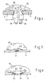
- FIGS. 1 to 4 show in sections a shielding part 10 which is to be arranged on a printed circuit board 11 of the electronic module within the housing.
- the circuit board 11 has a recess 12 which is formed for receiving a latching lug 13 of the shielding part 10.
- This locking lug 13 is part of the shielding member 10 and can be made with this by means of a punching operation of a sheet metal part.
- the dimensions of the latching lug 13 are initially selected so that the latching lug 13 can be guided through the recess 12 in the printed circuit board 11. However, the length of the latching lug 13 is greater than the thickness of the printed circuit board 11, so that the latching lug 13 projects beyond the printed circuit board 11.
- the shielding member 10 is fixed in position on the circuit board 11, but not yet secured against an outward movement from the recess 12.
- a stamped arcuate projection 14 is present.
- This projection 14 is briefly pushed back during insertion of the locking lug 13 in the recess 12, but jumps after the complete insertion of the locking lug 13 in the recess 12 back to its original position ( FIG. 1 , left view) back, so that thereby the shielding member 10 is fixed to the circuit board 11. It can not be easily removed now, then it requires such a force that the resilient projection 14 is pushed back again so far that the locking lug 13 can be pulled out of the recess 12.
- this spring force must have such a size that does not occur in normal operation of the electronic device.
- the shield member 10 has a shoulder 15, which ensures that the shielding member 10 with its the circuit board 11 facing the lower peripheral edge does not completely rests on the circuit board 11, but a distance is given.
- This paragraph 15 is in accordance with FIG. 1 arranged right and left of the latch 13, but can also be present at any other locations on the lower edge of the shield 10.
- FIG. 2 shows an embodiment as in FIG. 1 which, however, does not belong to the invention.
- a punched tab-shaped projection 16 is present, which also when inserting the locking lug 13 recedes into the recess 12 and jumps back after the full insertion back, so that thereby the locking lug 13 is fixed to the circuit board 11.
- the tab-shaped projection 16 can be easily and inexpensively manufactured by means of a punching process.
- FIG. 3 also shows a locking lug 13 which does not belong to the invention, which is inserted into the recess 12 of the circuit board 11.
- the locking lug 13 has a punctiform projection 17 (in particular two projections) which can be produced by compression deformation and are arranged on the locking lug 13 that they come to rest after complete insertion of the locking lug 13 into the recess 12 at the lower edge of the circuit board 11 in order to secure, as well as the projections 14 and 16, the shield 10 on the circuit board 11 securely.
- a punctiform projection 17 in particular two projections
- the detent 13 is resilient.
- the latching lug 13 has at least one slot 18, whereby two tabs 19 are formed, which have a greater longitudinal extent than the longitudinal extension of the recess 12.
- the longitudinal extent of the two tabs 19 and the width of the slot 18 are chosen such that that when inserting the latching lug 13 in the recess 12, the two tabs 12 are compressed and thus the latching lug 13 can be guided through the recess 12.
- the two tabs 19 spread apart again, wherein they advantageously do not assume their original position, but remain under bias.
- the shielding member 10 is fixed under a certain bias on the circuit board 11.
- the tabs 19 in their upper region bevels, with which they come to the lower edge of the circuit board 11 in the region of the recess 12 to the plant.
- the tabs 19 are made oblique to ensure a certain leadership when inserting.
- FIGS. 5 and 6 show embodiments that the shielding member 10 is contacted with a contact surface on the circuit board 11 electrically.
- the shielding part 10 has at least one pressure tab 20 which, for example, can again be punched out and shaped from the shielding part.
- the punched-out and preformed pressure flap 20 protrudes to some extent beyond the lower edge of the shielding part 10, so that it comes into contact with a contact surface 21 of the printed circuit board 11 under prestress and an electrical connection between the shielding part 10 and the contact surface 21 (ground connection). manufactures.
- FIG. 5 shows a single pressure tab 20 which is slightly angled at its end.
- FIG. 6 shows two opposite pressure tabs 20, which are each contacted with a contact surface 21 on the circuit board 11.
- the presence of more than one pressure tab 20 has the advantage that the contact reliability is increased, in the event that a pressure tab 20 is not sufficiently contacted the contact surface 21 or, for example, deformed due to damage and thus no contact is made.
- the shielding part 10 is formed as a shielding cage.
- This shielding cage is fixed on the circuit board in the manner described above and thus surrounds the electronic module, that is, the electronic components which are arranged on the circuit board, for the purpose of shielding.
- this shielding cage is thus effectively prevented that on the one hand emitted by the electronic module noise,
- it is also effectively prevented that interfering radiation from outside, eg from other electronic modules, can radiate into the shielded with the shielding electronic module.
- the electrical contacting of the Ablevoners 10 then takes place via the pressure tabs 20, which correspond to contact surfaces 21 on the circuit board 11 and / or via the FederbJech 6, which is provided on the shielding member 10 or on the inside of the housing, and the shielding member 10 electrically contacted the housing.
- This contacting takes place in a particularly advantageous manner when the electronic module is used with the shielding member 10 in the housing or the electronic module is already mounted on a base plate of the housing and then the housing is mounted for closing.
- the means according to the invention for electrical contacting between the shielding part 10 and the housing have in all variants the advantage that they can be produced simply and inexpensively, in particular in a stamping method or a stamping bending method, and at the same time a disassembly remains without causing a costly disassembly or destruction of the parts involved.
Landscapes
- Engineering & Computer Science (AREA)
- Microelectronics & Electronic Packaging (AREA)
- Shielding Devices Or Components To Electric Or Magnetic Fields (AREA)
Description
- Die Erfindung betrifft ein elektronisches hochfrequenztechnisches Gerät mit einem Gehäuse aus einem elektrisch leitfähigen Material gemäß den Merkmalen des Oberbegriffes des Patentanspruchs 1.
- In diesem Gehäuse des elektronischen Gerätes ist zur Realisierung der Funktion des elektronischen Gerätes zumindest ein elektronisches Modul, insbesondere mehrere Teilmodule, untergebracht. Diese Teilmodule können auf einer gemeinsamen Leiterplatte (Motherboard) angeordnet werden. Diese Anordnung kann beispielsweise über Steckverbinder erfolgen, so dass die Teilmodule, die ihrerseits aus Leiterplatten mit elektronischen Bauteilen bestehen, auf das Motherboard aufgesteckt werden. Aufgrund der Anwendung des elektronischen Gerätes im Hochfrequenzbereich ist es erforderlich, die einzelnen Module untereinander abzuschirmen, um Störungen bei deren Funktion und gegenseitige Beeinflussungen zu vermeiden. Hierzu ist schon vorgeschlagen worden, die einzelnen Module untereinander mittels Abschirmbleche hochfrequenzmäßig voneinander zu trennen bzw. mit einem Abschirmgehäuse zu umgeben. Diese Abschirmbleche bzw. Abschirmgehäuse werden auf dem Motherboard mit Masse kontaktiert, was zu einem gewissen Grad an Abschirmung führt, der allerdings noch nicht befriedigend ist. Außerdem ist es bekannt, dass die Abschirmteile unlösbar mit der Leiterplatte verbunden werden. Dies hat im Defektfall den Nachteil, dass das Abschirmteil nur unter Zerstörung von der Leiterplatte gelöst werden kann oder der Ablöseprozess äußerst aufwändig ist. Dies hat zur Folge, dass sich der Austausch eines defekten elektronischen Modules oder Teilmodules nicht mehr lohnt, da er zu teuer ist.
- Aus der
EP-A-1 130 953 ist ein elektronisches hochfrequenztechnisches Gerät mit einem Gehäuse aus einem elektrisch leitfähigen Material bekannt, wobei in dem Gehäuse zumindest ein elektronisches Modul sowie ein zugeordnetes Abschirmteil angeordnet ist und weiterhin das Abschirmteil Mittel zur lösbaren Befestigung an einer in dem Gehäuse angeordneten Leiterplatte aufweist. Die Mittel zur lösbaren Befestigung sind als Lasche mit Bohrung an den Abschirmteil ausgebildet, das mit einer Schraubverbindung an der Leiterplatte befestigt ist. - Aus der
US-A-6,297,967 ist ein Abschirmteil mit Mittel zur lösbaren Befestigung an einer Leiterplatte bekannt. - Aus der
EP-A-0 755 177 ist ein Abschirmteil mit Rastmitteln bekannt, bei dem das Abschirmteil einen Rasthaken aufweist, der durch eine Ausnehmung in einer Leiterplatte durchgeführt wird und die Unterseite der Leiterplatte hintergreift. - Der Erfindung liegt daher die Aufgabe zugrunde, ein elektronisches Gerät mit einem Gehäuse für hochfrequenztechnische Anwendungen bereitzustellen, bei dem die Abschirmung von Modulen oder Teilmodulen innerhalb des Gehäuses verbessert ist, um gegenseitige Beeinflussungen deutlich zu reduzieren, sowie bei dem einfache Montage- und auch Demontageschritte gegeben sind.
- Erfindungsgemäß ist vorgesehen, dass die Mittel als Rastmittel ausgebildet sind und die Rastmittel derart federnd ausgebildet ist, dass das Abschirmteil nach dem Festlegen an der Leiterplatte unter Vorspannung steht. Dadurch ist die Möglichkeit' gegeben, das Abschirmteil, schnell und einfach an der Leiterplatte zu befestigen, d.h. auf dieser anzuordnen, aber auch wieder zu demontieren. Die lösbare Befestigung ist in besonders vorteilhafter Weise eine Rastverbindung, wozu das Abschirmteil eine Rastnase mit einem Bogenförmigen vorsprung aufweist, die in eine entsprechende Ausnehmung in der Leiterplatte eingesteckt wird und nach dem vollständigen Einstecken verrastet. Dabei sind die Rastmittel, insbesondere die Rastnase und die korrespondierende Ausnehmung in der Leiterplatte so ausgestattet, dass nach der Verrastung das Abschirmteil zuverlässig und dauerhaltbar an der Leiterplatte festgelegt ist, aber im Falle der Demontage zwecks Austausch des elektronischen Modules einfach gelöst werden kann. Auch der umgekehrte Fall, dass die Leiterplatte einen Vorsprung aufweist und das Abschirmteil mit einer korrespondierenden Ausnehmung versehen ist, ist denkbar, aber auf Grund der aufwändigeren Konstruktion nicht bevorzugt. Denn es bietet sich in besonders vorteilhafter Weise an, dass das Abschirmteil, genau so wie schon die Mittel zur elektrischen Kontaktierung zwischen dem Gehäuse und dem Abschirmteil, aus einem elektrisch leitfähigen Blechmaterial bestehen und mittels eines Stanzverfahrens zwecks Formgebung bearbeitet werden. So können das Abschirmteil (Abschirmblech oder Abschirmgehäuse oder dergleichen) aus einem Blech ausgestanzt, gegebenenfalls umgeformt werden, wobei bei diesem Stanzvorgang auch gleichzeitig die Rastmittel mit angeformt werden. Bei der Formgebung der Rastmittel wird die Rastnase als laschenförmiges Element ausgebildet ist, welches einen bogen förmigen Vorsprung aufweist. Mit diesem Vorsprung wird die Rastnase zuverlässig an der Leiterplatte festgelegt.
- Mehrere Ausführungsbeispiele für die erfindungsgemäße einfache und kostengünstige Kontaktierung zwecks Herstellung einer elektrischen Masseverbindung bzw. Montage oder Demontage, auf die die Erfindung jedoch nicht beschränkt ist, sind im Folgenden beschrieben und anhand der Figuren erläutert.
- Es zeigen:
- Figuren 1 bis 4:
- verschiedene Ausgestaltungen einer Rastanase,
- Figuren 5 und 6:
- Ausgestaltungen von Drucklaschen an dem Abschirmteil,
- Figuren 7 und 8:
- Ansicht und Detailansicht eines als Abschirmkäfig ausgebildeten Abschirmteiles.
-
Figur 1 betrifft, soweit im Einzelnen dargestellt, ein Gehäuse eines elektronischen Gerätes für hochfrequenztechnische Anwendungen, so zum Beispiel ein TV-Tuner für den Fernsehempfang, hier insbesondere wieder zur Anwendung bei Fahrzeugen. Dieses Gehäuse ist Bestandteil eines mehrteiligen Gesamtgehäuses, das beispielsweise aus dem Gehäuse als Deckel und einem damit verbindbaren Boden besteht. Der Boden nimmt eine Grundplatine (Motherboard) auf, auf der wiederum mittels Steckverbindungen Teilmodule angeordnet sind. Diese Teilmodule sind beispielsweise senkrecht auf der Grundplatine angeordnet und stehen somit von dieser ab. Bekannt ist es, diese Teilmodule mit einer Abschirmung zu versehen, wobei diese Abschirmung beispielsweise als zwischen den Teilmodulen angeordnete Abschirmbleche ausgebildet ist. Ergänzend oder alternativ dazu können die Teilmodule von einem Abschirmgehäuse umgeben sein. Diese Abschirmbleche oder Abschirmgehäuse sind elektrisch mit einer Masse der Grundplatine kontaktiert. - Die
Figuren 1 bis 4 zeigen ausschnittweise ein Abschirmteil 10, das auf einer Leiterplatte 11 des elektronischen Modules innerhalb des Gehäuses anzuordnen ist. Zu diesem Zweck weist die Leiterplatte 11 eine Ausnehmung 12 auf, die zur Aufnahme einer Rastnase 13 des Abschirmteiles 10 ausgebildet ist. Diese Rastnase 13 ist Bestandteil des Abschirmteiles 10 und kann mit diesem mittels eines Stanzvorganges aus einem Blechteil hergestellt werden. Die Abmessungen der Rastnase 13 sind zunächst so gewählt, dass die Rastnase 13 durch die Ausnehmung 12 in der Leiterplatte 11 geführt werden kann. Allerdings ist die Länge der Rastnase 13 größer als die Dicke der Leiterplatte 11, so dass die Rastnase 13 über die Leiterplatte 11 übersteht. Damit ist zunächst das Abschirmteil 10 an der Leiterplatte 11 lagefixiert, allerdings noch nicht gegen eine Herausbewegung aus der Ausnehmung 12 gesichert. Zu diesem Zweck ist gemäßFigur 1 an der Rastnase 13 ein ausgestanzter bogenförmiger Vorsprung 14 vorhanden. Dieser Vorsprung 14 wird beim Einsetzen der Rastnase 13 in die Ausnehmung 12 kurzzeitig zurückgedrückt, springt aber nach dem vollständigen Einsetzen der Rastnase 13 in die Ausnehmung 12 wieder in seine Ursprungsposition (Figur 1 , linke Darstellung) zurück, so dass dadurch das Abschirmteil 10 an der Leiterplatte 11 festgelegt ist. Es kann nunmehr auch nicht ohne Weiteres abgenommen werden, dann dazu bedarf es einer solchen Kraft, dass der federnde Vorsprung 14 wieder so weit zurückgedrückt wird, dass die Rastnase 13 aus der Ausnehmung 12 herausgezogen werden kann. Diese Federkraft muss aber eine solche Größe aufweisen, die im normalen Betrieb des elektronischen Gerätes nicht vorkommt. Weiterhin ist inFigur 1 noch gezeigt, dass das Abschirmteil 10 einen Absatz 15 aufweist, der gewährleistet, dass das Abschirmteil 10 mit seiner der Leiterplatte 11 zugewandten unteren umlaufenden Kante nicht vollständig auf der Leiterplatte 11 aufliegt, sondern ein Abstand gegeben ist. Dieser Absatz 15 ist gemäßFigur 1 rechts und links von der Rastnase 13 angeordnet, kann aber auch an beliebigen anderen Stellen an der Unterkante des Abschirmteiles 10 vorhanden sein. -
Figur 2 zeigt eine Ausgestaltung wie beiFigur 1 , die jedoch nicht zur Erfindung gehört. Hier ist ein ausgestanzter laschenförmiger Vorsprung 16 vorhanden, der ebenfalls beim Einsetzen der Rastnase 13 in die Ausnehmung 12 zurückweicht und nach dem vollständigen Einsetzen wieder zurück springt, so dass dadurch die Rastnase 13 an der Leiterplatte 11 festgesetzt ist. Auch der laschenförmige Vorsprung 16 kann mittels eines Stanzverfahrens einfach und kostengünstig hergestellt werden. -
Figur 3 zeigt ebenfalls eine Rastnase 13 die nicht zur Erfindung gehört, die in die Ausnehmung 12 der Leiterplatte 11 eingesetzt wird. Hier weist die Rastnase 13 einen punktförmigen Vorsprung 17 (insbesondere zwei Vorsprünge), die durch Druckverformung herstellbar sind und so an der Rastnase 13 angeordnet werden, dass sie nach vollständigen Einsetzen der Rastnase 13 in die Ausnehmung 12 an der Unterkante der Leiterplatte 11 zur Anlage kommen, um damit, genau so wie die Vorsprünge 14 und 16, das Abschirmteil 10 an der Leiterplatte 11 sicher festlegen. - In
Figur 4 ist gezeigt, dass die Rastnase 13 federnd ausgebildet ist. Zu diesem Zweck weist die Rastnase 13 zumindest einen Schlitz 18 auf, wodurch sich zwei Laschen 19 bilden, die eine größere Längserstreckung haben, als die Längserstreckung der Ausnehmung 12. Dabei ist die Längserstreckung der beiden Laschen 19 und die Breite des Schlitzes 18 so gewählt, dass beim Einsetzen der Rastnase 13 in die Ausnehmung 12 die beiden Laschen 12 zusammengedrückt und damit die Rastnase 13 durch die Ausnehmung 12 geführt werden kann. Nachdem dies erfolgt ist, spreizen sich die beiden Laschen 19 wieder auseinander, wobei sie in vorteilhafter Weise nicht ihre ursprüngliche Lage einnehmen, sondern unter Vorspannung bleiben. Damit ist auch das Abschirmteil 10 unter einer gewissen Vorspannung an der Leiterplatte 11 festgelegt. Zum Toleranzausgleich weisen die Laschen 19 in ihrem oberen Bereich Abschrägungen auf, mit denen sie an der Unterkante der Leiterplatte 11 im Bereich der Ausnehmung 12 zur Anlage kommen. Zwecks einfacher Einführung der Rastnase 13 in die Ausnehmung 12 sind die Laschen 19 schräg ausgeführt, um eine gewisse Führung beim Einsetzen zu gewährleisten. - Obwohl in den
Figuren 1 bis 3 jeweils Absätze 15 gezeigt sind, können diese in dieser Form vorhanden sein, aber auch an anderer Stelle an dem Abschirmteil vorhanden sein oder gänzlich entfallen. - Die
Figuren 5 und 6 zeigen Ausgestaltungen dafür, dass das Abschirmteil 10 mit einer Kontaktfläche an der Leiterplatte 11 elektrisch kontaktiert wird. Zu diesem Zweck weist das Abschirmteil 10 zumindest eine Drucklasche 20 auf, die beispielsweise wieder aus dem Abschirmteil ausgestanzt und geformt sein kann. Dabei steht die ausgestanzte und vorgeformte Drucklasche 20 in gewissem Maß über der unteren Kante des Abschirmteiles 10 hervor, so dass sie mit einer Kontaktfläche 21 der Leiterplatte 11 unter Vorspannung zur Anlage kommt und eine elektrische Verbindung zwischen dem Abschirmteil 10 und der Kontaktfläche 21 (Masseverbindung) herstellt.Figur 5 zeigt eine einzige Drucklasche 20, die an ihrem Endbereich leicht abgewinkelt ist.Figur 6 zeigt zwei gegenüberliegende Drucklaschen 20, die jeweils mit einer Kontaktfläche 21 auf der Leiterplatte 11 kontaktiert sind. Das Vorhandensein von mehr als einer Drucklasche 20 hat den Vorteil, dass die Kontaktsicherheit gesteigert ist, für den Fall, dass eine Drucklasche 20 nicht ausreichend die Kontaktfläche 21 kontaktiert oder z.B. auf Grund einer Beschädigung verformt ist und somit keine Kontaktierung gegeben ist. - In den
Figuren 7 und 8 ist gezeigt, dass das Abschirmteil 10 als Abschirmkäfig ausgebildet ist. Dieser Abschirmkäfig wird auf der Leiterplatte in der vorstehend beschriebenen Weise festgelegt und umgibt damit das elektronische Modul, d.h., die elektronischen Bauteile, die auf der Leiterplatte angeordnet sind, zwecks Abschirmung. Mit diesem Abschirmkäfig wird also wirksam verhindert, dass einerseits von dem elektronischen Modul Störstrahlungen ausgesandt werden, andererseits wird aber auch wirksam verhindert, dass Störstrahlungen von außerhalb, z.B. von anderen elektronischen Modulen, in das mit dem Abschirmkäfig abgeschirmte elektronische Modul einstrahlen können. Zwecks Abschirmung ist es also erforderlich, dass zumindest eine elektronische Modul innerhalb des Gehäuses mit dem Abschirmkäfig zu versehen. Im Regelfall werden innerhalb des Gehäuses mehrere elektronische (Teil-) Module angeordnet sein, die jeweils einen Abschirmkäfig aufweisen oder zwischen denen ein Abschirmblech angeordnet ist. Da zur Sicherstellung der Abschirmung das Abschirmteil auf einem bestimmten elektrischen Potenzial (insbesondere Masse) liegen muss, werden erfindungsgemäß die beiden Alternativen zur Montage und gleichzeitige elektrischen Kontaktierung vorgeschlagenen Lösungen realisiert. Mit Blick auf dieFiguren 7 und 8 kann also ein solches Abschirmteil 10 mit den entsprechend ausgebildeten Rastnasen 13 einfach und schnell auf der Leiterplatte 11 (hier nicht dargestellt) montiert und demontiert werden. Die elektrische Kontaktierung des Abschirmteiles 10 erfolgt dann über die Drucklaschen 20, die mit Kontaktflächen 21 auf der Leiterplatte 11 korrespondieren und/oder über das FederbJech 6, welches an dem Abschirmteil 10 oder an der Innenseite des Gehäuses vorhanden ist, und das Abschirmteil 10 elektrisch mit dem Gehäuse kontaktiert. Diese Kontaktierung erfolgt in besonders vorteilhafter Weise, wenn das elektronische Modul mit dem Abschirmteil 10 in das Gehäuse eingesetzt wird bzw. das elektronische Modul schon auf einer Grundplatte des Gehäuses montiert ist und anschließend das Gehäuse zum Verschließen montiert wird. - Die erfindungsgemäßen Mittel zur elektrischen Kontaktierung zwischen dem Abschirmteil 10 und dem Gehäuse haben in allen Varianten den Vorteil, dass sie einfach und kostengünstig, insbesondere in einem Stanzverfahren oder einem Stanzbiegeverfahren, herstellbar sind und gleichzeitig eine Demontage bestehen bleibt, ohne dass es zu einer aufwändigen Demontage oder einer Zerstörung der beteiligten Teile kommt.
-
- 10.
- Abschirmteil
- 11.
- Leiterplatte
- 12.
- Ausnehmung
- 13.
- Rastnase
- 14.
- ausgestanzter bogenförmiger Vorsprung
- 15.
- Absatz
- 16.
- ausgestanzter laschenförmiger Vorsprung
- 17.
- punktförmiger Vorsprung
- 18.
- Schlitz
- 19.
- Lasche
- 20.
- Drucklasche
- 21.
- Kontaktfläche
Claims (4)
- Elektronisches hochfrequenztechnisches Gerät mit einem Gehäuse aus einem elektrisch leitfähigen Material, wobei in dem Gehäuse zumindest ein elektronisches Modul sowie ein zugeordnetes Abschirmteil (10) angeordnet ist, wobei das Abschirmteil (10) Mittel zur lösbaren Befestigung an einer in dem Gehäuse angeordneten Leiterplatte (11) aufweist, dadurch gekennzeichet, dass die Mittel als Rastmittel ausgebildet sind und die Rastmittel derart federnd ausgebildet sind, dass das Abschirmteil (10) nach dem Festlegen an der Leiterplatte (11) unter Vorspannung steht wobei die Rastnase (13) einen bogenförmigen Vorsprung (14) aufweist, und das Gerät ein TV-Tuner für den Fernsehempfeng zur Anwendung bei Fahrzeugen ist.
- Gerät nach Anspruch 1, dadurch gekennzeichnet, dass die Rastmittel als eine Rastnase (13) ausgebildet sind.
- Gerät nach einem der vorhergehenden Ansprüche, dadurch gekennzeichnet, dass das Abschirmteil (10) als Abschirmblech oder Abschirmkäfig ausgebildet ist.
- Gerät nach einem der vorhergehenden Ansprüche, dadurch gekennzeichnet, dass das Abschirmteil (10) mittels eines Stanzbiegeverfahrens aus einem Blech herstellbar ist.
Applications Claiming Priority (5)
| Application Number | Priority Date | Filing Date | Title |
|---|---|---|---|
| DE102004012565 | 2004-03-12 | ||
| DE102004012565 | 2004-03-12 | ||
| DE200510010271 DE102005010271A1 (de) | 2004-03-12 | 2005-03-03 | Federblech in einem Gehäuse als Abschirmung für ein elektronisches hochfrequenztechnisches Gerät |
| DE102005010271 | 2005-03-03 | ||
| EP05004888A EP1575347B1 (de) | 2004-03-12 | 2005-03-05 | Federblech in einem Gehäuse als Abschirmung für ein elektronisches hochfrequenztechnisches Gerät |
Related Parent Applications (2)
| Application Number | Title | Priority Date | Filing Date |
|---|---|---|---|
| EP05004888.3 Division | 2005-03-05 | ||
| EP05004888A Division EP1575347B1 (de) | 2004-03-12 | 2005-03-05 | Federblech in einem Gehäuse als Abschirmung für ein elektronisches hochfrequenztechnisches Gerät |
Publications (2)
| Publication Number | Publication Date |
|---|---|
| EP1603381A1 EP1603381A1 (de) | 2005-12-07 |
| EP1603381B1 true EP1603381B1 (de) | 2012-10-31 |
Family
ID=34813701
Family Applications (1)
| Application Number | Title | Priority Date | Filing Date |
|---|---|---|---|
| EP05013745A Expired - Lifetime EP1603381B1 (de) | 2004-03-12 | 2005-03-05 | Federblech in einem Gehäuse als Abschirmung für ein elektronisches hochfrequenztechnisches Gerät |
Country Status (1)
| Country | Link |
|---|---|
| EP (1) | EP1603381B1 (de) |
Families Citing this family (4)
| Publication number | Priority date | Publication date | Assignee | Title |
|---|---|---|---|---|
| EP2299796A3 (de) * | 2009-09-18 | 2011-06-01 | Bang & Olufsen A/S | Abschirmkasten |
| CN103108521B (zh) * | 2013-01-15 | 2016-06-22 | 深圳市华星光电技术有限公司 | 前框结构、显示装置及显示装置的制作方法 |
| WO2022218532A1 (en) * | 2021-04-15 | 2022-10-20 | Telefonaktiebolaget Lm Ericsson (Publ) | A housing for an electrical component |
| EP4679962A1 (de) * | 2024-07-09 | 2026-01-14 | Aptiv Technologies AG | Abschirmung mit kombinierter pressung und oberflächenmontagekompression |
Family Cites Families (3)
| Publication number | Priority date | Publication date | Assignee | Title |
|---|---|---|---|---|
| EP0755177B1 (de) * | 1995-07-21 | 1999-01-20 | Molex Incorporated | Abschirmdeckel mit zugehörigem Abschirmverfahren |
| GB2322012B (en) * | 1997-02-05 | 2001-07-11 | Nokia Mobile Phones Ltd | Self securing RF screened housing |
| JP3270028B2 (ja) * | 1999-09-10 | 2002-04-02 | 株式会社ソニー・コンピュータエンタテインメント | 電磁シールド板、電磁シールド構造体及びエンタテインメント装置 |
-
2005
- 2005-03-05 EP EP05013745A patent/EP1603381B1/de not_active Expired - Lifetime
Also Published As
| Publication number | Publication date |
|---|---|
| EP1603381A1 (de) | 2005-12-07 |
Similar Documents
| Publication | Publication Date | Title |
|---|---|---|
| DE10006530A1 (de) | Antennenfeder | |
| WO2004008823A1 (de) | Abschirmeinrichtung für elektronische baugruppen auf einer leiterplatte | |
| EP2683230A1 (de) | Kastengehäuse | |
| DE102017123761A1 (de) | Verbinder-aufbau | |
| DE10223170A1 (de) | EMV-Abschirmung für elektronische Bauelemente und EMV-Gehäuse | |
| DE102012111183A1 (de) | Radareinrichtung für ein Fahrzeug | |
| EP3378289B1 (de) | Leiterplatte zum mechanischen fixieren eines gehäuses | |
| WO1996031104A1 (de) | Steuergerät für ein kraftfahrzeug | |
| DE60004222T2 (de) | Verfahren und vorrichtung zur abschirmung einer steckeranordnung mit elastischen fingern | |
| WO2001069729A1 (de) | Steckverbindung | |
| EP2689496B1 (de) | Direktsteckelement, insbesondere für fahrzeugsteuergeräte | |
| EP0886999B1 (de) | Abdeckvorrichtung mit niedriger bauhöhe für elektromagnetisch abgeschirmte metallische gehäuse | |
| EP1603381A1 (de) | Federblech in einem Gehäuse als Abschirmung für ein elektronisches hochfrequenztechnisches Gerät | |
| DE102012005812A1 (de) | Elektrischer Verbinder mit integriertem Impedanzangleichelement | |
| EP1905121B1 (de) | Träger zur aufnahme eines antennenverstärkers eines fahrzeuges | |
| DE102005033664A1 (de) | Federblech in einem Gehäuse als Abschirmung für ein elektronisches hochfrequenztechnisches Gerät | |
| DE102009058181A1 (de) | Träger für Leiterplatte | |
| EP1575347B1 (de) | Federblech in einem Gehäuse als Abschirmung für ein elektronisches hochfrequenztechnisches Gerät | |
| DE102005010271A1 (de) | Federblech in einem Gehäuse als Abschirmung für ein elektronisches hochfrequenztechnisches Gerät | |
| EP1229604B1 (de) | Funkbaugruppe mit Antenne | |
| DE29604599U1 (de) | Elektromagnetisch abgeschirmtes Gehäuse mit über eine Kontaktfederleiste verrastbaren metallischen Gehäuseteilen | |
| EP1467608B1 (de) | Abschirmung für ein Hochfrquenzgerät, insbesondere einen TV-Tuner eines Fahrzeuges | |
| DE102005056953B3 (de) | Computergehäuse mit einem Abschirmblech mit mindestens einer Öffnung und Herstellungsverfahren für einen Computer | |
| EP0886998B1 (de) | Eckprofilleiste für elektromagnetisch abgeschirmten baugruppenträger | |
| EP0984515B1 (de) | Abgeschirmter elektrischer Steckverbinder |
Legal Events
| Date | Code | Title | Description |
|---|---|---|---|
| PUAI | Public reference made under article 153(3) epc to a published international application that has entered the european phase |
Free format text: ORIGINAL CODE: 0009012 |
|
| AC | Divisional application: reference to earlier application |
Ref document number: 1575347 Country of ref document: EP Kind code of ref document: P |
|
| AK | Designated contracting states |
Kind code of ref document: A1 Designated state(s): AT BE BG CH CY CZ DE DK EE ES FI FR GB GR HU IE IS IT LI LT LU MC NL PL PT RO SE SI SK TR |
|
| AX | Request for extension of the european patent |
Extension state: AL BA HR LV MK YU |
|
| 17P | Request for examination filed |
Effective date: 20051213 |
|
| AKX | Designation fees paid |
Designated state(s): AT BE BG CH CY CZ DE DK EE ES FI FR GB GR HU IE IS IT LI LT LU MC NL PL PT RO SE SI SK TR |
|
| GRAP | Despatch of communication of intention to grant a patent |
Free format text: ORIGINAL CODE: EPIDOSNIGR1 |
|
| RAP1 | Party data changed (applicant data changed or rights of an application transferred) |
Owner name: HIRSCHMANN CAR COMMUNICATION GMBH |
|
| GRAS | Grant fee paid |
Free format text: ORIGINAL CODE: EPIDOSNIGR3 |
|
| GRAA | (expected) grant |
Free format text: ORIGINAL CODE: 0009210 |
|
| AC | Divisional application: reference to earlier application |
Ref document number: 1575347 Country of ref document: EP Kind code of ref document: P |
|
| AK | Designated contracting states |
Kind code of ref document: B1 Designated state(s): AT BE BG CH CY CZ DE DK EE ES FI FR GB GR HU IE IS IT LI LT LU MC NL PL PT RO SE SI SK TR |
|
| REG | Reference to a national code |
Ref country code: GB Ref legal event code: FG4D Free format text: NOT ENGLISH Ref country code: CH Ref legal event code: EP |
|
| REG | Reference to a national code |
Ref country code: AT Ref legal event code: REF Ref document number: 582605 Country of ref document: AT Kind code of ref document: T Effective date: 20121115 |
|
| REG | Reference to a national code |
Ref country code: IE Ref legal event code: FG4D Free format text: LANGUAGE OF EP DOCUMENT: GERMAN |
|
| REG | Reference to a national code |
Ref country code: DE Ref legal event code: R096 Ref document number: 502005013218 Country of ref document: DE Effective date: 20121227 |
|
| REG | Reference to a national code |
Ref country code: LT Ref legal event code: MG4D |
|
| REG | Reference to a national code |
Ref country code: NL Ref legal event code: VDEP Effective date: 20121031 |
|
| PG25 | Lapsed in a contracting state [announced via postgrant information from national office to epo] |
Ref country code: ES Free format text: LAPSE BECAUSE OF FAILURE TO SUBMIT A TRANSLATION OF THE DESCRIPTION OR TO PAY THE FEE WITHIN THE PRESCRIBED TIME-LIMIT Effective date: 20130211 Ref country code: IS Free format text: LAPSE BECAUSE OF FAILURE TO SUBMIT A TRANSLATION OF THE DESCRIPTION OR TO PAY THE FEE WITHIN THE PRESCRIBED TIME-LIMIT Effective date: 20130228 Ref country code: NL Free format text: LAPSE BECAUSE OF FAILURE TO SUBMIT A TRANSLATION OF THE DESCRIPTION OR TO PAY THE FEE WITHIN THE PRESCRIBED TIME-LIMIT Effective date: 20121031 Ref country code: LT Free format text: LAPSE BECAUSE OF FAILURE TO SUBMIT A TRANSLATION OF THE DESCRIPTION OR TO PAY THE FEE WITHIN THE PRESCRIBED TIME-LIMIT Effective date: 20121031 Ref country code: FI Free format text: LAPSE BECAUSE OF FAILURE TO SUBMIT A TRANSLATION OF THE DESCRIPTION OR TO PAY THE FEE WITHIN THE PRESCRIBED TIME-LIMIT Effective date: 20121031 Ref country code: SE Free format text: LAPSE BECAUSE OF FAILURE TO SUBMIT A TRANSLATION OF THE DESCRIPTION OR TO PAY THE FEE WITHIN THE PRESCRIBED TIME-LIMIT Effective date: 20121031 |
|
| PG25 | Lapsed in a contracting state [announced via postgrant information from national office to epo] |
Ref country code: SI Free format text: LAPSE BECAUSE OF FAILURE TO SUBMIT A TRANSLATION OF THE DESCRIPTION OR TO PAY THE FEE WITHIN THE PRESCRIBED TIME-LIMIT Effective date: 20121031 Ref country code: GR Free format text: LAPSE BECAUSE OF FAILURE TO SUBMIT A TRANSLATION OF THE DESCRIPTION OR TO PAY THE FEE WITHIN THE PRESCRIBED TIME-LIMIT Effective date: 20130201 Ref country code: CY Free format text: LAPSE BECAUSE OF FAILURE TO SUBMIT A TRANSLATION OF THE DESCRIPTION OR TO PAY THE FEE WITHIN THE PRESCRIBED TIME-LIMIT Effective date: 20121031 Ref country code: PT Free format text: LAPSE BECAUSE OF FAILURE TO SUBMIT A TRANSLATION OF THE DESCRIPTION OR TO PAY THE FEE WITHIN THE PRESCRIBED TIME-LIMIT Effective date: 20130228 Ref country code: PL Free format text: LAPSE BECAUSE OF FAILURE TO SUBMIT A TRANSLATION OF THE DESCRIPTION OR TO PAY THE FEE WITHIN THE PRESCRIBED TIME-LIMIT Effective date: 20121031 |
|
| REG | Reference to a national code |
Ref country code: HU Ref legal event code: AG4A Ref document number: E015430 Country of ref document: HU |
|
| PG25 | Lapsed in a contracting state [announced via postgrant information from national office to epo] |
Ref country code: DK Free format text: LAPSE BECAUSE OF FAILURE TO SUBMIT A TRANSLATION OF THE DESCRIPTION OR TO PAY THE FEE WITHIN THE PRESCRIBED TIME-LIMIT Effective date: 20121031 Ref country code: EE Free format text: LAPSE BECAUSE OF FAILURE TO SUBMIT A TRANSLATION OF THE DESCRIPTION OR TO PAY THE FEE WITHIN THE PRESCRIBED TIME-LIMIT Effective date: 20121031 Ref country code: BG Free format text: LAPSE BECAUSE OF FAILURE TO SUBMIT A TRANSLATION OF THE DESCRIPTION OR TO PAY THE FEE WITHIN THE PRESCRIBED TIME-LIMIT Effective date: 20130131 Ref country code: SK Free format text: LAPSE BECAUSE OF FAILURE TO SUBMIT A TRANSLATION OF THE DESCRIPTION OR TO PAY THE FEE WITHIN THE PRESCRIBED TIME-LIMIT Effective date: 20121031 |
|
| PG25 | Lapsed in a contracting state [announced via postgrant information from national office to epo] |
Ref country code: IT Free format text: LAPSE BECAUSE OF FAILURE TO SUBMIT A TRANSLATION OF THE DESCRIPTION OR TO PAY THE FEE WITHIN THE PRESCRIBED TIME-LIMIT Effective date: 20121031 Ref country code: RO Free format text: LAPSE BECAUSE OF FAILURE TO SUBMIT A TRANSLATION OF THE DESCRIPTION OR TO PAY THE FEE WITHIN THE PRESCRIBED TIME-LIMIT Effective date: 20121031 |
|
| PLBE | No opposition filed within time limit |
Free format text: ORIGINAL CODE: 0009261 |
|
| STAA | Information on the status of an ep patent application or granted ep patent |
Free format text: STATUS: NO OPPOSITION FILED WITHIN TIME LIMIT |
|
| BERE | Be: lapsed |
Owner name: HIRSCHMANN CAR COMMUNICATION G.M.B.H. Effective date: 20130331 |
|
| 26N | No opposition filed |
Effective date: 20130801 |
|
| PG25 | Lapsed in a contracting state [announced via postgrant information from national office to epo] |
Ref country code: MC Free format text: LAPSE BECAUSE OF NON-PAYMENT OF DUE FEES Effective date: 20130331 |
|
| REG | Reference to a national code |
Ref country code: CH Ref legal event code: PL |
|
| REG | Reference to a national code |
Ref country code: DE Ref legal event code: R097 Ref document number: 502005013218 Country of ref document: DE Effective date: 20130801 |
|
| REG | Reference to a national code |
Ref country code: IE Ref legal event code: MM4A |
|
| PG25 | Lapsed in a contracting state [announced via postgrant information from national office to epo] |
Ref country code: BE Free format text: LAPSE BECAUSE OF NON-PAYMENT OF DUE FEES Effective date: 20130331 Ref country code: LI Free format text: LAPSE BECAUSE OF NON-PAYMENT OF DUE FEES Effective date: 20130331 Ref country code: IE Free format text: LAPSE BECAUSE OF NON-PAYMENT OF DUE FEES Effective date: 20130305 Ref country code: CH Free format text: LAPSE BECAUSE OF NON-PAYMENT OF DUE FEES Effective date: 20130331 |
|
| REG | Reference to a national code |
Ref country code: AT Ref legal event code: MM01 Ref document number: 582605 Country of ref document: AT Kind code of ref document: T Effective date: 20130305 |
|
| PG25 | Lapsed in a contracting state [announced via postgrant information from national office to epo] |
Ref country code: AT Free format text: LAPSE BECAUSE OF NON-PAYMENT OF DUE FEES Effective date: 20130305 |
|
| PG25 | Lapsed in a contracting state [announced via postgrant information from national office to epo] |
Ref country code: LU Free format text: LAPSE BECAUSE OF NON-PAYMENT OF DUE FEES Effective date: 20130305 |
|
| REG | Reference to a national code |
Ref country code: FR Ref legal event code: PLFP Year of fee payment: 12 |
|
| REG | Reference to a national code |
Ref country code: FR Ref legal event code: PLFP Year of fee payment: 13 |
|
| REG | Reference to a national code |
Ref country code: FR Ref legal event code: PLFP Year of fee payment: 14 |
|
| REG | Reference to a national code |
Ref country code: DE Ref legal event code: R082 Ref document number: 502005013218 Country of ref document: DE Representative=s name: WILHELM & BECK, DE |
|
| PGFP | Annual fee paid to national office [announced via postgrant information from national office to epo] |
Ref country code: FR Payment date: 20230110 Year of fee payment: 19 Ref country code: CZ Payment date: 20230215 Year of fee payment: 19 |
|
| PGFP | Annual fee paid to national office [announced via postgrant information from national office to epo] |
Ref country code: TR Payment date: 20230303 Year of fee payment: 19 Ref country code: HU Payment date: 20230118 Year of fee payment: 19 Ref country code: GB Payment date: 20230112 Year of fee payment: 19 Ref country code: DE Payment date: 20230110 Year of fee payment: 19 |
|
| REG | Reference to a national code |
Ref country code: DE Ref legal event code: R119 Ref document number: 502005013218 Country of ref document: DE |
|
| PG25 | Lapsed in a contracting state [announced via postgrant information from national office to epo] |
Ref country code: CZ Free format text: LAPSE BECAUSE OF NON-PAYMENT OF DUE FEES Effective date: 20240305 |
|
| PG25 | Lapsed in a contracting state [announced via postgrant information from national office to epo] |
Ref country code: CZ Free format text: LAPSE BECAUSE OF NON-PAYMENT OF DUE FEES Effective date: 20240305 |
|
| GBPC | Gb: european patent ceased through non-payment of renewal fee |
Effective date: 20240305 |
|
| PG25 | Lapsed in a contracting state [announced via postgrant information from national office to epo] |
Ref country code: HU Free format text: LAPSE BECAUSE OF NON-PAYMENT OF DUE FEES Effective date: 20240306 |
|
| PG25 | Lapsed in a contracting state [announced via postgrant information from national office to epo] |
Ref country code: HU Free format text: LAPSE BECAUSE OF NON-PAYMENT OF DUE FEES Effective date: 20240306 |
|
| PG25 | Lapsed in a contracting state [announced via postgrant information from national office to epo] |
Ref country code: DE Free format text: LAPSE BECAUSE OF NON-PAYMENT OF DUE FEES Effective date: 20241001 |
|
| PG25 | Lapsed in a contracting state [announced via postgrant information from national office to epo] |
Ref country code: GB Free format text: LAPSE BECAUSE OF NON-PAYMENT OF DUE FEES Effective date: 20240305 |
|
| PG25 | Lapsed in a contracting state [announced via postgrant information from national office to epo] |
Ref country code: FR Free format text: LAPSE BECAUSE OF NON-PAYMENT OF DUE FEES Effective date: 20240331 |
|
| PG25 | Lapsed in a contracting state [announced via postgrant information from national office to epo] |
Ref country code: GB Free format text: LAPSE BECAUSE OF NON-PAYMENT OF DUE FEES Effective date: 20240305 Ref country code: FR Free format text: LAPSE BECAUSE OF NON-PAYMENT OF DUE FEES Effective date: 20240331 Ref country code: DE Free format text: LAPSE BECAUSE OF NON-PAYMENT OF DUE FEES Effective date: 20241001 |