EP1601010A2 - Herstellung von schrägen Gräben - Google Patents
Herstellung von schrägen Gräben Download PDFInfo
- Publication number
- EP1601010A2 EP1601010A2 EP05104486A EP05104486A EP1601010A2 EP 1601010 A2 EP1601010 A2 EP 1601010A2 EP 05104486 A EP05104486 A EP 05104486A EP 05104486 A EP05104486 A EP 05104486A EP 1601010 A2 EP1601010 A2 EP 1601010A2
- Authority
- EP
- European Patent Office
- Prior art keywords
- wafer
- plasma
- oblique
- recesses
- protuberances
- Prior art date
- Legal status (The legal status is an assumption and is not a legal conclusion. Google has not performed a legal analysis and makes no representation as to the accuracy of the status listed.)
- Withdrawn
Links
Images

Classifications
-
- H—ELECTRICITY
- H10—SEMICONDUCTOR DEVICES; ELECTRIC SOLID-STATE DEVICES NOT OTHERWISE PROVIDED FOR
- H10P—GENERIC PROCESSES OR APPARATUS FOR THE MANUFACTURE OR TREATMENT OF DEVICES COVERED BY CLASS H10
- H10P50/00—Etching of wafers, substrates or parts of devices
- H10P50/69—Etching of wafers, substrates or parts of devices using masks for semiconductor materials
- H10P50/691—Etching of wafers, substrates or parts of devices using masks for semiconductor materials for Group V materials or Group III-V materials
- H10P50/693—Etching of wafers, substrates or parts of devices using masks for semiconductor materials for Group V materials or Group III-V materials characterised by their size, orientation, disposition, behaviour or shape, in horizontal or vertical plane
-
- H—ELECTRICITY
- H10—SEMICONDUCTOR DEVICES; ELECTRIC SOLID-STATE DEVICES NOT OTHERWISE PROVIDED FOR
- H10P—GENERIC PROCESSES OR APPARATUS FOR THE MANUFACTURE OR TREATMENT OF DEVICES COVERED BY CLASS H10
- H10P76/00—Manufacture or treatment of masks on semiconductor bodies, e.g. by lithography or photolithography
- H10P76/40—Manufacture or treatment of masks on semiconductor bodies, e.g. by lithography or photolithography of masks comprising inorganic materials
- H10P76/408—Manufacture or treatment of masks on semiconductor bodies, e.g. by lithography or photolithography of masks comprising inorganic materials characterised by their sizes, orientations, dispositions, behaviours or shapes
Definitions
- the present invention relates to the production of recesses, holes or trenches in a material, and applies particularly in the field of semiconductor materials, intended for the production of discrete or integrated electronic components.
- the invention relates more particularly to the realization of recesses, holes or trenches oblique to a main surface of the material to be etched and having a dimension transverse small.
- one of the processes commonly used, particularly in the field of microelectronics, is an etching process plasma.
- FIG. 1 illustrates schematically a reactor plasma etching.
- the reactor comprises an enclosure 1 provided with of a bottom 2 on which is placed a support or susceptor 3, which can be isolated from the bottom 2.
- a plate 4 in which we want perform engraving operations is placed on the support 3.
- a plasma 5 is created by any means in the enclosure, for example by a radio frequency field, and can be confined by fields electromagnetic.
- the enclosure also includes means, not shown, of introduction, circulation and extraction of gas, and possibly means of implementation. temperature, for example cooling, support 3 and than means of polarization of this support.
- the plasma usually extends into the entire enclosure, and in any case in the vicinity of the plate burn 4, and is separated from all internal surfaces of the enclosure by a distance s, in which there is a zone neutral, called sheath.
- the plasmas are often made to from fluorinated or chlorinated gases.
- anisotropic mechanisms involve two mechanisms: a mechanism engraving and a passivation mechanism that can be alternated or not. It is considered that the engraving mechanism involves two phenomena, on the one hand a bombardment by the ions is finding in the plasma, on the other hand a chemical attack by reactive substances in the plasma. These two phenomena are inseparable. Ionic bombardment is used to remove reaction products placed at the bottom a recess during training.
- FIG. 2 is a sectional view of a plate 4, coated with a masking layer 7 comprising openings 8, disposed in the plasma etching reactor of Figure 1, that is, a plasma region separated from the wafer by a sheath thickness s.
- Ions bombard the silicon wafer normally on the surface of it and are active, with species chemicals in the plasma at openings 8 in the mask 7 to engrave in the plate 4 recesses 10 orthogonal to the surface of the wafer.
- anisotropic plasma etching techniques do not normally not allow for non-recess orthogonal to a main surface of a wafer to be treated.
- Japanese Patent Application 2002-134470 proposes to to deflect ions through a lateral field created at the level of the surface of a wafer. This field results from an accumulation of charge under insulators of different thicknesses, the difference of thickness being of the order of 100 nm. It is unlikely that this process makes it possible to obtain deep trenches to obtain angles of inclination of significant values.
- An oblique trench will for example be made with a saw diamond (JP-A-56054066), by sanding (JP-A-03225961), with laser (EP-A-0070692) or else by oblique ionic etching (JP-A-08130220 and JP-A-62173737). These various methods do not allow not to obtain thin trenches and / or to create patterns complex shape.
- the present invention proposes a modification of usual methods of plasma etching to achieve recesses, trenches or vias extending obliquely by ratio to the surface of a wafer and not just perpendicular to it, these recesses may have small lateral dimensions, as conventionally obtained by plasma etching.
- the present invention provides a method of forming an oblique dimension recess less than 10 ⁇ m in a wafer arranged in a plasma etching reactor in which the plasma extends along of the surface of the wafer, consisting of forming discontinuities in the contour of the plasma and its sheath at immediate vicinity of the wafer in areas where wish to form recesses delimited by openings in a protective mask on the surface of the wafer.
- the discontinuities result for example protuberances formed on the plate.
- the present invention is based on observation according to which, in a conventional plasma etching process, the engraving is of course orthogonal to the surface of the plate to engrave but especially that it occurs perpendicular to the plasma surface at the boundary of the sheath.
- the present invention proposes to deform the contour of the plasma so that ions, projected orthogonally at this contour, will be projected in a non direction parallel to the surface of the wafer.
- this deformation of the plasma contour is achieved by forming protuberances on the surface of the wafer.
- protuberances on the surface of the wafer.
- other means could be envisaged to distort this outline of the plasma.
- Figure 3 illustrates an embodiment of the present invention.
- a mask 12 provided with openings 13.
- a protuberance 15 is formed on the wafer. This protuberance can be achieved by depositing and engraving of a thick layer and its surface will eventually be provided with a coating 16 to make it insensitive to etching by the plasma.
- the contour of the plasma is deformed in the vicinity of the protuberance, as indicated by the dashed line 18 and includes in particular a rounded area 19 in the vicinity of feet of the protuberance.
- the paths Ion bombardment are orthogonal to this curvature, that is to say, have an oblique relation to the surface of the plate 11. It will thus be possible to form oblique recesses 21 in the plate.
- the inclination of the recesses 21 depends on the proximity of the openings 13 in the mask 12 with respect to foot of the protuberance 15. Plus the openings 13 in the 12 are close to the foot of the protrusion 15, plus the recesses will be oblique.
- the distance between the protuberances 15.1 and 15.2 is sufficient for the sheath to be deformed and the plasma penetrates more or less deeply between the protuberances, that is, the distance between two protuberances must be greater than the sheath thickness s.
- the sheath thickness is commonly, according to the conditions of the plasma, a value of 0.1 to 0.6 mm. These values are given only as examples and will depend on plasma conditions in the reactor as well as the type of reactor.
- the sheath thickness s is increased by increasing the pressure in the enclosure. So, to get a deformation of the shape of the sheath protuberances with a height of at least 100 ⁇ m, preferably of the same order of thickness as the thickness s of the sheath.
- All the variants of plasma etching can be used, including various substrate polarization systems and various possible cooling systems of the substrate as well as various gas circulation systems in the enclosure.
- the substrate to be engraved is a silicon wafer
- the apparent surfaces of the second wafer will be preferably oxidized to prevent etching of the silicon by the plasma.
- the invention has the advantage of allow to form in a wafer recesses, vias or oblique trenches of a width well below 10 ⁇ m, which is well below the minimum dimension that we know currently realize using saws.
- plasma etching one can commonly proceed to the engraving of recesses whose minimum dimensions are well below a micrometer but up to a few micrometers, and the depth of the recesses formed can extend to depths of the order of a few micrometers but up to a few hundred micrometers.
- the protuberances 15 may take the form of rectilinear ribs if one wants to form recesses 21 in form of straight trenches.
- the protuberances 15 can also take the form of circular counters, or any chosen shape, centered on corresponding openings 13 formed in the mask 12; the recesses 21 will then have the shaped inverted truncated cones.
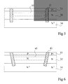
- Figures 5 and 6 illustrate an example of application of the present invention to the realization of a high voltage diode vertical, Figure 5 illustrating a conventional structure and Figure 6 illustrating a structure according to the present invention.
- the diode is formed from a substrate 32 weakly doped N type whose upper face comprises a region 33 doped type P and whose lower face includes a region 34 strongly doped N.
- An active zone is delimited by a trench 31 whose walls are coated with an insulator, for example of silicon oxide. Trench 31 crosses the layer P 33 and, at least partially, the substrate 32. not shown cathode metallization is formed on the face lower and an anode metallization not shown is formed on the upper face on the active zone.
- the equipotentials represented by dots, extend substantially horizontally and are distributed mainly in layer 32.
- the equipotentials are closer together at the periphery of the component, in the vicinity of the vertical trench 31, only in the central part.
- the thickness of the N-type layer 32 must therefore be greater than its theoretical thickness to allow withstand the voltage without breakdown at the periphery of the component.
- the equipotentials 36 become horizontal even in the peripheral region.
- the diode will have a better resistance in tension and the chosen thickness for the lightly doped N-type region may be close to its theoretical value.
- the trench oblique device can be performed in one or many stages. It may also consist of a succession of neighboring holes (in the manner of dotted lines) joining as a result of an oxidation step.
Landscapes
- Drying Of Semiconductors (AREA)
Applications Claiming Priority (2)
| Application Number | Priority Date | Filing Date | Title |
|---|---|---|---|
| FR0451038 | 2004-05-26 | ||
| FR0451038 | 2004-05-26 |
Publications (2)
| Publication Number | Publication Date |
|---|---|
| EP1601010A2 true EP1601010A2 (de) | 2005-11-30 |
| EP1601010A3 EP1601010A3 (de) | 2009-01-21 |
Family
ID=34939976
Family Applications (1)
| Application Number | Title | Priority Date | Filing Date |
|---|---|---|---|
| EP05104486A Withdrawn EP1601010A3 (de) | 2004-05-26 | 2005-05-25 | Herstellung von schrägen Gräben |
Country Status (2)
| Country | Link |
|---|---|
| US (1) | US7226870B2 (de) |
| EP (1) | EP1601010A3 (de) |
Families Citing this family (3)
| Publication number | Priority date | Publication date | Assignee | Title |
|---|---|---|---|---|
| EP2333821A4 (de) * | 2008-09-01 | 2014-07-30 | Japan Science & Tech Agency | Plasmaätzverfahren, plasmaätzgerät und verfahren zur herstellung eines photonischen kristalls |
| ITUA20164724A1 (it) | 2016-06-28 | 2017-12-28 | St Microelectronics Srl | Dispositivo elettronico a semiconduttori con migliorate caratteristiche di testabilita' e relativo metodo di incapsulamento |
| EP4020024A1 (de) | 2020-12-22 | 2022-06-29 | Paul Scherrer Institut | Verfahren zur herstellung einer fächerförmigen optik mit hohem aspektverhältnis |
Family Cites Families (14)
| Publication number | Priority date | Publication date | Assignee | Title |
|---|---|---|---|---|
| JPS5654066A (en) * | 1979-10-08 | 1981-05-13 | Toshiba Corp | Production of bevel type semiconductor |
| GB2102202A (en) * | 1981-07-17 | 1983-01-26 | Westinghouse Brake & Signal | Semiconductor device passivation |
| JPS62173737A (ja) * | 1986-01-27 | 1987-07-30 | Mitsubishi Electric Corp | 半導体装置 |
| JPH01286436A (ja) * | 1988-05-13 | 1989-11-17 | Fujitsu Ltd | 半導体装置の製造方法 |
| JPH03225961A (ja) * | 1990-01-31 | 1991-10-04 | Meidensha Corp | 半導体素子 |
| EP0498254B1 (de) * | 1991-01-28 | 1996-03-27 | Sony Corporation | Mikroelektronischer ballistischer Transistor und Verfahren zu seiner Herstellung |
| JPH08130220A (ja) * | 1994-10-31 | 1996-05-21 | Nkk Corp | 半導体装置におけるコンタクト部およびその形成方法 |
| US6563079B1 (en) * | 1999-02-25 | 2003-05-13 | Seiko Epson Corporation | Method for machining work by laser beam |
| US7018780B2 (en) * | 1999-06-25 | 2006-03-28 | Lam Research Corporation | Methods for controlling and reducing profile variation in photoresist trimming |
| US6316169B1 (en) * | 1999-06-25 | 2001-11-13 | Lam Research Corporation | Methods for reducing profile variation in photoresist trimming |
| TW457567B (en) * | 2000-07-17 | 2001-10-01 | Mosel Vitelic Inc | Manufacturing method for gate oxide layer |
| JP3376348B2 (ja) * | 2000-10-20 | 2003-02-10 | 株式会社半導体先端テクノロジーズ | 半導体装置の製造方法、及び半導体装置 |
| US6528332B2 (en) * | 2001-04-27 | 2003-03-04 | Advanced Micro Devices, Inc. | Method and system for reducing polymer build up during plasma etch of an intermetal dielectric |
| US6844959B2 (en) * | 2002-11-26 | 2005-01-18 | Reflectivity, Inc | Spatial light modulators with light absorbing areas |
-
2005
- 2005-05-25 EP EP05104486A patent/EP1601010A3/de not_active Withdrawn
- 2005-05-26 US US11/138,804 patent/US7226870B2/en not_active Expired - Lifetime
Also Published As
| Publication number | Publication date |
|---|---|
| EP1601010A3 (de) | 2009-01-21 |
| US20050263486A1 (en) | 2005-12-01 |
| US7226870B2 (en) | 2007-06-05 |
Similar Documents
| Publication | Publication Date | Title |
|---|---|---|
| US8278183B2 (en) | Production of isolation trenches with different sidewall dopings | |
| EP0057126B1 (de) | Verfahren zur Herstellung einer Transistorstruktur | |
| FR3021455A1 (fr) | Procede d'aplanissement d'evidements remplis de cuivre | |
| US7833909B2 (en) | Method of manufacturing semiconductor device, and etching apparatus | |
| EP0005721A1 (de) | Verfahren zur Herstellung eines Bipolartransistors mit einem Basiskontakt aus Polysilicium und einem Emitterkontakt aus Polysilicium oder Metall | |
| FR2832547A1 (fr) | Procede de realisation d'une diode schottky sur substrat de carbure de silicium | |
| EP3876288A1 (de) | Bildung eines thyristors, triacs oder einer diode zur unterdrückung von transienten spannungen | |
| EP2800722A1 (de) | Verfahren zum ätzen eines komplexen musters | |
| EP1111669A1 (de) | Verfahren zur Herstellung von isolierten metallischen Verbindungsleitungen in integrierten Schaltkreisen | |
| FR2984594A1 (fr) | Procede de realisation d'une tranchee profonde dans un substrat de composant microelectronique | |
| EP0273792B1 (de) | Verfahren zur Herstellung von Elementen mit Zwischenraum | |
| EP0275778A1 (de) | Verfahren zum chemischen gemeinsamen Zerteilen von Halbleiterbauelementen und nach diesem Verfahren getrennte Bauelemente | |
| FR2879024A1 (fr) | Peripherie de composant unipolaire vertical | |
| FR3091002A1 (fr) | Procédé de gravure d’une couche diélectrique tridimensionnelle | |
| CN101483195A (zh) | 具有沟道形场环结构的功率半导体元件 | |
| WO2008065143A1 (fr) | Procede de realisation d'un substrat mixte | |
| EP2998998A1 (de) | Ätzungsverfahren an der oberfläche einer 3d-struktur | |
| US7226870B2 (en) | Forming of oblique trenches | |
| FR2979478A1 (fr) | Procede de realisation d'une tranchee profonde dans un substrat de composant microelectronique | |
| EP0997931A1 (de) | Verfahren zur Bildung einer isolierenden Seitenwand in einem Halbleitersubstrat | |
| FR3100085A1 (fr) | procédé de fabrication de composants micro-électroniques | |
| EP4053884B1 (de) | Verfahren zum ätzen einer dielektrischen dreidimensionalen schicht | |
| FR3098644A1 (fr) | Procédé de formation d’espaceurs d’un transistor | |
| FR3131658A1 (fr) | Procédé de formation d'une cavité | |
| FR3152190A1 (fr) | Procédé de réalisation de motifs sur un substrat |
Legal Events
| Date | Code | Title | Description |
|---|---|---|---|
| PUAI | Public reference made under article 153(3) epc to a published international application that has entered the european phase |
Free format text: ORIGINAL CODE: 0009012 |
|
| AK | Designated contracting states |
Kind code of ref document: A2 Designated state(s): AT BE BG CH CY CZ DE DK EE ES FI FR GB GR HU IE IS IT LI LT LU MC NL PL PT RO SE SI SK TR |
|
| AX | Request for extension of the european patent |
Extension state: AL BA HR LV MK YU |
|
| PUAL | Search report despatched |
Free format text: ORIGINAL CODE: 0009013 |
|
| AK | Designated contracting states |
Kind code of ref document: A3 Designated state(s): AT BE BG CH CY CZ DE DK EE ES FI FR GB GR HU IE IS IT LI LT LU MC NL PL PT RO SE SI SK TR |
|
| AX | Request for extension of the european patent |
Extension state: AL BA HR LV MK YU |
|
| RIC1 | Information provided on ipc code assigned before grant |
Ipc: H01L 21/033 20060101ALI20081217BHEP Ipc: H01L 29/861 20060101ALI20081217BHEP Ipc: H01L 21/762 20060101ALI20081217BHEP Ipc: H01L 21/308 20060101AFI20050907BHEP |
|
| AKX | Designation fees paid | ||
| REG | Reference to a national code |
Ref country code: DE Ref legal event code: 8566 |
|
| STAA | Information on the status of an ep patent application or granted ep patent |
Free format text: STATUS: THE APPLICATION IS DEEMED TO BE WITHDRAWN |
|
| 18D | Application deemed to be withdrawn |
Effective date: 20090722 |