EP1600237A1 - Jet soldering apparatus - Google Patents
Jet soldering apparatus Download PDFInfo
- Publication number
- EP1600237A1 EP1600237A1 EP03769946A EP03769946A EP1600237A1 EP 1600237 A1 EP1600237 A1 EP 1600237A1 EP 03769946 A EP03769946 A EP 03769946A EP 03769946 A EP03769946 A EP 03769946A EP 1600237 A1 EP1600237 A1 EP 1600237A1
- Authority
- EP
- European Patent Office
- Prior art keywords
- solder
- jet nozzle
- dropped
- guide
- molten solder
- Prior art date
- Legal status (The legal status is an assumption and is not a legal conclusion. Google has not performed a legal analysis and makes no representation as to the accuracy of the status listed.)
- Withdrawn
Links
Images




Classifications
-
- B—PERFORMING OPERATIONS; TRANSPORTING
- B23—MACHINE TOOLS; METAL-WORKING NOT OTHERWISE PROVIDED FOR
- B23K—SOLDERING OR UNSOLDERING; WELDING; CLADDING OR PLATING BY SOLDERING OR WELDING; CUTTING BY APPLYING HEAT LOCALLY, e.g. FLAME CUTTING; WORKING BY LASER BEAM
- B23K1/00—Soldering, e.g. brazing, or unsoldering
- B23K1/08—Soldering by means of dipping in molten solder
-
- B—PERFORMING OPERATIONS; TRANSPORTING
- B23—MACHINE TOOLS; METAL-WORKING NOT OTHERWISE PROVIDED FOR
- B23K—SOLDERING OR UNSOLDERING; WELDING; CLADDING OR PLATING BY SOLDERING OR WELDING; CUTTING BY APPLYING HEAT LOCALLY, e.g. FLAME CUTTING; WORKING BY LASER BEAM
- B23K3/00—Tools, devices or special appurtenances for soldering, e.g. brazing, or unsoldering, not specially adapted for particular methods
- B23K3/06—Solder feeding devices; Solder melting pans
- B23K3/0646—Solder baths
- B23K3/0653—Solder baths with wave generating means, e.g. nozzles, jets, fountains
-
- H—ELECTRICITY
- H05—ELECTRIC TECHNIQUES NOT OTHERWISE PROVIDED FOR
- H05K—PRINTED CIRCUITS; CASINGS OR CONSTRUCTIONAL DETAILS OF ELECTRIC APPARATUS; MANUFACTURE OF ASSEMBLAGES OF ELECTRICAL COMPONENTS
- H05K3/00—Apparatus or processes for manufacturing printed circuits
- H05K3/30—Assembling printed circuits with electric components, e.g. with resistors
- H05K3/32—Assembling printed circuits with electric components, e.g. with resistors electrically connecting electric components or wires to printed circuits
- H05K3/34—Assembling printed circuits with electric components, e.g. with resistors electrically connecting electric components or wires to printed circuits by soldering
-
- H—ELECTRICITY
- H05—ELECTRIC TECHNIQUES NOT OTHERWISE PROVIDED FOR
- H05K—PRINTED CIRCUITS; CASINGS OR CONSTRUCTIONAL DETAILS OF ELECTRIC APPARATUS; MANUFACTURE OF ASSEMBLAGES OF ELECTRICAL COMPONENTS
- H05K3/00—Apparatus or processes for manufacturing printed circuits
- H05K3/30—Assembling printed circuits with electric components, e.g. with resistors
- H05K3/32—Assembling printed circuits with electric components, e.g. with resistors electrically connecting electric components or wires to printed circuits
- H05K3/34—Assembling printed circuits with electric components, e.g. with resistors electrically connecting electric components or wires to printed circuits by soldering
- H05K3/3465—Application of solder
- H05K3/3468—Application of molten solder, e.g. dip soldering
Definitions
- the present invention relates to a soldering apparatus, and more specifically to a flow soldering apparatus suitable for miniaturization of the soldering apparatus.
- One of the flow soldering apparatuses performs soldering in that a printed circuit board is first soldered with a primary jet nozzle, and then a secondary jet nozzle adjusts soldering defects such as bridges, icicles, etc. caused through the soldering procedure of the primary jet nozzle (refer to, for example, Japanese Patent Application Laid-Open No. H9-8450).
- a surface of solder has been oxidized which then produces impurities called dross.
- a surface of a solder layer may be filled with inert gas (refer to, for example, Japanese Patent Application Laid-Open No.
- the flow soldering apparatus may be provided with a dispersion protective-shield for foreign matters, which covers an upper portion where molten solder flowed and dropped from the nozzle strongly collides against a solder surface in a solder tank or flow from another nozzle (refer to, for example, Japanese Patent Application Laid-Open No. 5-305432).
- the molten solder both flowed from the primary jet nozzle and the secondary jet nozzle in the solder tank is moved downward and met each other between the jet nozzles.
- the dross tends to build up at the merging point D. Once the dross occurs, it spreads as covering the surface of the solder, and the dross eventually spreads upward over the surface flowed from the primary jet nozzle and the secondary jet nozzle.
- the interval between the solder flowed from the primary jet nozzle and the secondary jet nozzle is generally kept at 5 cm or more.
- the foregoing flow soldering apparatuses have had the following drawbacks. Because the dross spreads upward over the flowed surface of the primary jet nozzle and the secondary jet nozzle, the dross attaches to the solder surface of the circuit board which causes soldering defects such as bridges, icicles, etc.. Considering cost and productivity, the above soldering manner may be appropriate for home-use electrical products but cannot be applied to fine-pitch electronic components since the bridges cannot be eliminated completely. For the circuit board with the fine-pitch electronic components which is soldered in the conventional solder tank, operators need to perform visual inspection to solder portions after the circuit board is soldered. In case the bridges are detected, the operators are required to repair the circuit board with an iron, which hampers productivity.
- the interval between the solder flowed from the primary jet nozzle and the secondary jet nozzle has approximately 5 cm
- the solder attached to the circuit board cools down while the circuit board moves between the jet nozzles, whereby the performance of the soldering at the secondary jet nozzle becomes deteriorated.
- the above-mentioned flow soldering apparatuses have difficulties to be miniaturized.
- the lead-free solder has a high-melting point (approximately 230°C) compared to a conventional solder (approximately 183°C).
- the lead-free solder is thus more affected by the temperature drop-down on the circuit board than the conventional solder. Accordingly, in order to use the lead-free solder, the interval between the primary jet nozzle and the secondary jet nozzle needs to be further reduced for preventing the solder from dropping-down of the temperature.
- the present invention has been made in light of the above problem, and it is an object of the present invention to provide a compact soldering apparatus applicable for a lead-free solder while reducing an occurrence of dross to improve product reliability.
- a V-shaped guide plate provided with solder guide portions is placed, so that the molten solder flowed from the primary jet nozzle and the secondary jet nozzle is dropped on a nozzle side different to a nozzle side where the solder is flowed.
- the guide plate is made of a material to which solder is not attached.
- the guide plate is provided with stripe-shaped solder guide portions alternately configured in the direction of a ridge line of a plate bent into a V-shape.
- a solder separator is provided between the stripe-shaped solder guide portions formed on the guide plate.
- the guide plate is formed by placing two pieces of plates into a V-shape and has a space along a ridge line of the V-shaped guide plate.
- the guide plate is formed in such a manner that some of the independent solder guide portions are alternately provided in the direction of the ridge line.
- a solder tank 6 reservoiring molten solder S comprises a primary jet nozzle 1, a secondary jet nozzle 2 and a pump (not shown) forming jet waves 24, 25.
- Guide plates 4, 5 placed between the jet nozzles 1, 2 are provided at a position above a solder face F of the molten solder S.
- the guide plates 4, 5 are provided at a position where the molten solder flowed from both the primary jet nozzle 1 and the secondary jet nozzle 2 in the solder tank 6 is dropped.
- the guide plates 4, 5 are formed in a V-shape with solder guide portions 4a, 5a to be described later(see Figs. 2 and 3) so that the molten solder S is dropped at different positions on the solder face F in the solder tank 6.
- Jet openings 1a, 2a are incurvated and are provided at two places where the jet waves 24, 25 formed by the jet nozzles 1, 2 provided in the solder tank 6 and a circuit board P transported in the direction of arrow A with a conveyer (not shown) meet each other.
- the bottom ends of the incurvation are placed above the molten solder S.
- Jet opening 2b is bent upward so as to refrain the molten solder flowed by the jet opening 2b from flowing over the molten solder S.
- the molten solder S reservoired in the solder tank 6 is flowed with the pump (not shown) so as to form the jet waves 24, 25.
- the circuit board P is transported to the jet waves 24, 25 and soldered by being in contact to the jet waves 24, 25.
- the guide plates 4, 5 are formed in a manner that a flat plate 10, which is a piece of a material having anti-stick quality to solder, for example, stainless steel, is punched through, and the flat plate 10 is bent into a V-shape at an approximate center portion R.
- the guide plates 4, 5 each has the stripe-shaped solder guide portions 4a, 5a so as to make the molten solder S dropped at different positions on the solder face F in the solder tank 6.
- solder guide portions 4a, 5a are bent into the V-shape at the approximate center portion R so as to make the solder guide portions 4a, 5a cross each other. Portions where the solder guide portions 4a, 5a cross thus have spaces W.
- the molten solder which is dropped along the solder guide portions 4a, 5a passes through the spaces W and is dropped on the solder face F which is opposite side of the guide plate where the molten solder is dropped. That is, the molten solder is dropped on the nozzle side different to the nozzle side where the solder is flowed.
- solder guide portions 4a, 5a are placed above the solder face F, it is possible to have another configurations as long as the center portion R is placed above the solder face F. However, it is preferable if the solder guide portions 4a, 5a are placed above the solder face F.
- the angle of the V-shape, the position and the size of the solder guide portions 4a, 5a should be properly determined in consideration of viscosity of the molten solder, the transport speed of the circuit board P, etc., so that the molten solder in the solder tank flowed from the primary jet nozzle and the secondary jet nozzle does not merge each other when dropping thereby optimally preventing the accumulation of the dross.
- the solder guide portions 4a, 5a have a solder separator G therebetween so as to separate the molten solder flowed from the jet openings.
- the solder separator G is made to stand at a cutting portion 50 by bending in the direction that the molten solder is dropped. It does not matter which sides of the jet nozzles 1, 2 the guide plates 4, 5 are placed to, but, for making understanding easier, as shown in Fig. 1, the guide plate 5 and the guide plate 4 are placed to the primary jet nozzle 1 and the secondary jet nozzle 2, respectively.
- the function of the guide plates 4, 5 is explained hereinafter according to Fig. 3.
- the molten solder K is dropped onto upper portions 41, 51 of the guide plates 4, 5 provided at a position where the molten solder K in the solder tank flowed from the primary jet nozzle 1 and the secondary jet nozzle 2 is dropped.
- the molten solder K flowing from the primary jet nozzle 1 is dropped on the guide plate 5.
- the space W is formed at a point where the solder guide portions 4a, 5a cross.
- the molten solder K dropped at a position where the solder guide portion 5a is formed is passed through the space W and dropped along the solder guide portion 5a.
- the molten solder K is then dropped to the solder face F on the side where the secondary jet nozzle 2 in the solder tank 6 is placed. Also, among the molten solder K dropped on the guide plate 5, the molten solder K dropped onto a position where the solder separator G is formed is separated with the solder separator G and dropped along the solder guide portion 5a provided at both sides. The molten solder K is then dropped on the solder face F at a proximal position where the secondary jet nozzle 2 is placed in the solder tank 6.
- the molten solder K flowing from the secondary jet nozzle 2 is dropped on the guide plate 4.
- the molten solder K dropped at a position where the solder guide portion 4a is formed is made to drop along the solder guide portion 4a and passed through the space W.
- the molten solder K is then dropped to the solder face F on the side where the primary jet nozzle 1 is placed in the solder tank 6.
- the molten solder K dropped onto a position where the solder separator G is formed is separated with the solder separator G and dropped along the solder guide portion 4a provided at both sides.
- the molten solder K is then dropped on the solder face F at a proximal position where the primary jet nozzle 1 is placed in the solder tank 6.
- the guide plates 4, 5 function in such a manner that the molten solder K flowed from the primary jet nozzle 1 and the molten solder K flowed from the secondary jet nozzle 2 is dropped at different sides on which the molten solder was flowed. Because the guide plates 4, 5 are formed in that each of the solder guide portions 4a, 5a is alternately configured in the direction of the ridge line R formed by bending the plate into the V-shape, the molten solder K flowed from the same nozzle is also dropped at different positions on the solder face F in the solder tank 6. Specifically, the molten solder K is dropped at positions, which are separated by width of the solder guide portion 4a or the solder guide portion 5a.
- the molten solder K flowed and dropped from the primary jet nozzle 1 and the secondary jet nozzle 2 in the solder tank does not merge each other. Further, the molten solder dropped at either position d1 or d2, which are separated by width of either the solder guide portion 4a or the solder guide portion 5a, interact each other prohibiting the dross built up between the primary jet nozzle and the secondary jet nozzle.
- the guide plates 4, 5 are shown in broken-lines; details thereof are omitted.
- the circuit board P is conveyed over the primary jet nozzle 1 in the direction of arrow A with the conveyer (not shown).
- the circuit board P first contacts to the jet wave 24 formed by the primary jet nozzle 1 and then contacts to the jet wave 25 formed by the secondary jet nozzle 2.
- the circuit board P further proceeds and is detached from the flow soldering apparatus.
- the excess of the molten solder is dropped onto upper portions of the guide plates 4, 5.
- the molten solder K which is flowed from the primary jet nozzle 1 and the secondary jet nozzle 2 and dropped onto the upper portions of the guide plates 4, 5, is made to drop on the nozzle side different to the nozzle side where the solder is flowed as shown in Fig. 1. Furthermore, since the guide plates 4, 5 are formed in that each of the solder guide portions 4a, 5a is alternately configured in the direction of the ridge line formed by bending the plate into the V-shape, the molten solder K flowed from the same nozzle is also dropped at different positions on the solder face F in the solder tank 6.
- the molten solder K is dropped at the positions d1 and d2, which are separated by width of either the solder guide portion 4a or the solder guide portion 5a.
- the molten solder K flowed and dropped from the primary jet nozzle 1 and the secondary jet nozzle 2 in the solder tank does not thus merge each other.
- the molten solder dropped at either position d1 or d2, which is separated by width of either the solder guide portion 4a or the solder guide portion 5a interact each other prohibiting the accumulation of the dross between the primary jet nozzle and the secondary jet nozzle.
- the angle of the V-shape in the guide plates 4, 5 is made to be small, the distance between the molten solder K flowed and dropped from the primary jet nozzle and the secondary jet nozzle becomes narrow, whereas the distance therebetween becomes wide when the angle gets large. Accordingly, in consideration of the distance between the primary jet nozzle and the secondary set nozzle and the cool-down of the solder attached to the substrate, the angle of the V-shape should be wider as much as possible so as to prohibit the merging of the molten solder K and the accumulation of the dross between the primary jet nozzle and the secondary jet nozzle.
- the angle of the V-shape should be thus properly determined based on not only the position and the size of the solder guide portions 4a, 5a but also the viscosity of the molten solder, the conveying speed of the circuit board P, etc.. Because the guide plates are formed into the V-shape as discussed above, the angle of the V-shape can be easily adjusted according to properties that the solder tank owns, for example, the distance between the primary jet nozzle and the secondary jet nozzle.
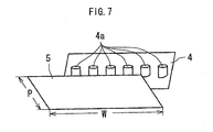
- FIG. 6 shows the embodiment of the guide plates 4, 5 in which two pieces of individual plates are placed into a V-shape as shown in Fig. 7 and Fig. 8.
- a solder tank 6 reservoiring molten solder S comprises a primary jet nozzle 1, a secondary nozzle 2 and a pump (not shown) forming jet waves 24, 25. Between the primary jet nozzle 1 and the secondary jet nozzle 2, the guide plates 4, 5 are placed above a solder face F of the molten solder S.
- the guide plates 4, 5 are placed at where molten solder K in the solder tank 6 flowed from the primary jet nozzle and the secondary jet nozzle is dropped.
- the guide plates 4, 5 are formed by placing two pieces of the plates into the V-shape while a space SP is provided along a ridge line of the guide plates 4, 5 in the V-shape.
- solder guide portions 4a, 5a hereinafter explained are omitted from Fig. 6.
- bottom ends of the guide plates 4, 5 have the space SP whereby the molten solder K dropped on the guide plates 4, 5 falls on the nozzle side different to the nozzle side where the solder is flowed.
- Each of the solder guide portions 4a, 5a is provided on a position where the molten solder K is made to drop at different positions on the solder face F in the solder tank 6.
- each of the solder guide portions 4a has a distance 2L therebetween while each of the solder guide portions 5a has a distance 2L therebetween, and the solder guide portions 4a, 5a stand on the V-shaped guide plates 4, 5, which is perpendicular to the solder face F.
- the distance between the solder guide portion 4a and the solder guide portion 5a has a distance L, and each of the solder guide portions 4a, 5a is provided alongside and alternately.
- the shape of the solder guide portions 4a, 5a is not limited to the cylindrical bar but may be a triangle bar, polygonal bar such as square bar, etc. or an elliptic bar.
- the angle of the V-shape, the position and the size of the solder guide portions 4a, 5a, and the space SP should be suitably determined in consideration of viscosity of the molten solder K, a transport speed of the circuit board P, etc., so that the molten solder K in the solder tank flowed from the primary jet nozzle and the secondary jet nozzle does not merge each other when being dropped thereby optimally preventing the accumulation of the dross between the jet nozzles.
- each of the guide plates 4, 5 has 250-350 mm in width W, a diameter ⁇ and a height of the cylindrical solder guide portions 4a, 5a are 5-10 mm and 10-20 mm respectively, and the distance L between the solder guide portion 4a and the solder guide portion 5a is 25 mm.
- the numbers of the solder guide portions 4a, 5a are around 10-20.
- the space SP between the guide plates 4, 5 should be properly determined in consideration of the length P, slope, etc. of the guide plates 4, 5, whereby the molten solder flowed from the primary jet nozzle and the secondary jet nozzle falls on the nozzle side different to the nozzle side where the solder is flowed.
- the guide plates 4, 5 serve as follows.
- the guide plates 4, 5 can be provided at any sides of the jet nozzles 1, 2, but, for making understanding easier, as shown in Fig. 6, the guide plate 5 and the guide plate 4 are assumed to be provided at the primary jet nozzle 1 and the secondary nozzle 2, respectively. That is, the molten solder K is dropped on upper portions of the guide plates 4, 5 provided at a position where the molten solder K in the solder tank flowed from the primary jet nozzle 1 and the secondary jet nozzle 2 is dropped. The molten solder K flowing from the primary jet nozzle 1 is dropped on the guide plate 5.
- the molten solder K dropped on the guide plate 5 the molten solder K dropped at a position where the solder guide portion 5a is not formed is passed through between the solder guide portions 5a. The molten solder K is then dropped to the solder face F on the side where the secondary jet nozzle 2 in the solder tank 6 is placed. Also, among the molten solder K dropped on the guide plate 5, the molten solder K dropped on a position where the solder guide portion 5a is provided is separated with the solder guide portion 5a and dropped on the solder face F on the side where the secondary jet nozzle 2 in the solder tank 6 is placed.
- the molten solder K flowing from the secondary jet nozzle 2 is dropped on the guide plate 5.
- the molten solder K dropped at a position where the solder guide portion 5a is not formed is dropped between the solder guide portions 5a.
- the molten solder K is then dropped to the solder face F on the side where the secondary jet nozzle 2 in the solder tank 6 is placed.
- the molten solder K dropped on a position where the solder guide portion 5a is provided is separated with the solder guide portion 5a and dropped on the solder face F on the side where the primary jet nozzle 1 in the solder tank 6 is placed.
- the guide plates 4, 5 function in such a manner that the molten solder flowed from the primary jet nozzle 1 and the molten solder jetted from the secondary jet nozzle 2 drop at different sides on which the molten solder was flowed. Because the guide plates 4, 5 are formed in that each of the solder guide portions 4a, 5a is alternately configured in the direction of a ridge line formed by placing two pieces of plates into a V-shape, the molten solder K flowed from the same nozzle is also dropped at different positions on the solder face F in the solder tank 6. Specifically, the molten solder K is dropped at positions separated by width L of either the solder guide portion 4a or the solder guide portion 5a.
- the molten solder K flowed and dropped from the primary jet nozzle 1 and the secondary jet nozzle 2 in the solder tank does not merge each other thereby prohibiting the accumulation of the dross between the primary jet nozzle and the secondary jet nozzle.
- the circuit board P is conveyed over the primary jet nozzle 1 in the direction of arrow A with the conveyer (not shown).
- the circuit board P first contacts to the jet wave 24 formed by the primary jet nozzle 1 and then contacts to the jet wave 25 formed by the secondary jet nozzle 2.
- the circuit board P further proceeds and is detached from the flow soldering apparatus.
- the excess of the molten solder is dropped onto upper portions of the guide plates 4, 5.
- the molten solder K dropped onto the upper portions of the guide plates 4, 5 drops on the nozzle side different to the nozzle side where the solder is flowed as shown in Fig. 6. Furthermore, since the guide plates 4, 5 are formed in that each of the solder guide portions 4a, 5a is alternately configured in the direction of the ridge line formed by placing two pieces of plates into a V-shape, the molten solder K flowed from the same nozzle is also dropped at different positions on the solder face F in the solder tank 6. That is, the molten solder K is dropped at position d1 or d2 separated by width of either the solder guide portion 4a or the solder guide portion 5a. As shown in Fig.
- the molten solder flowed and dropped from the primary jet nozzle 1 and the secondary jet nozzle 2 in the solder tank does not thus merge each other. Further, the molten solder dropped at either position d1 or d2, which is separated by width of either the solder guide portion 4a or the solder guide portion 5a, interact each other prohibiting the accumulation of the dross between the primary jet nozzle and the secondary jet nozzle.
- a V-shaped guide plate provided with solder guide portions is placed, so that the molten solder flowed from the primary jet nozzle and the secondary jet nozzle drops on a nozzle side different to the nozzle side where the solder is flowed. Accordingly, an interval between the primary jet nozzle and the secondary jet nozzle can be shortened, whereby the solder does not cool down while the circuit board moves between the primary jet nozzle and the secondary jet nozzle, preventing occurrence of soldering failure, bridges, icicles, etc. and thus maintaining soldering performance. Because the interval between the jet nozzles can be shortened, miniaturization of the flow soldering apparatus is possible. Since the solder does not cool down, lead-free solder is applicable, thus considerably contributing to environmental protection.
- the guide plate is made of a material to which the solder is not attached, whereby not only maintenance of the guide plate such as cleaning, exchanging, etc. is not required, but also the molten solder is made to drop smoothly, which can maintain temperature of the molten solder in a solder tank, thus reducing an energy consumption.
- a solder separator is provided between the stripe-shaped solder guide portions formed on the guide plate, thus the molten solder dropped on upper portions placed between the solder guide portions passes through between the solder guide portions, which prevents the molten solder from dropping on the nozzle side same to the nozzle side where the solder is flowed. Accordingly, the molten solder in the solder tank flowed from the primary jet nozzle and the secondary jet nozzle does not merge each other when dropping thereby effectively preventing the accumulation of the dross between the primary jet nozzle and the secondary jet nozzle.
- the guide plate which is formed by placing two pieces of plates into a V-shape, has a space along a ridge line of the V-shaped guide plate, whereby position and speed at which the molten solder is dropped can be optionally determined. As a result, position of the primary jet nozzle and the secondary jet nozzle in the solder tank can be more freely determined.
Landscapes
- Engineering & Computer Science (AREA)
- Mechanical Engineering (AREA)
- Manufacturing & Machinery (AREA)
- Microelectronics & Electronic Packaging (AREA)
- Molten Solder (AREA)
- Electric Connection Of Electric Components To Printed Circuits (AREA)
Abstract
A compact soldering apparatus capable of increasing reliability of products by
reducing occurrence of dross and using lead-free solder, wherein a primary jet nozzle 1, a
secondary jet nozzle 2, and a pump (not shown) forming jet waves 24, 25 are installed in
a solder tank 6 reservoiring molten solder S. Guide plates 4, 5 are installed between
the jet nozzles 1, 2 above a solder face F of the molten solder S on a position where the
molten solder is dropped. The guide plates 4, 5 formed into a V-shape are provided
with solder guide portions crossing each other so as to drop the molten solder S at
different positions on the solder face F of the solder tank 6. Molten solder dropped onto
upper portions of the guide plates 4, 5 passes through the solder guide portions and is
made to fall on a nozzle side different to a nozzle side where the solder is flowed.
Description
The present invention relates to a soldering apparatus, and more
specifically to a flow soldering apparatus suitable for miniaturization of the soldering
apparatus.
One of the flow soldering apparatuses performs soldering in that a
printed circuit board is first soldered with a primary jet nozzle, and then a secondary jet
nozzle adjusts soldering defects such as bridges, icicles, etc. caused through the
soldering procedure of the primary jet nozzle (refer to, for example, Japanese Patent
Application Laid-Open No. H9-8450). In this type of the flow soldering apparatus, a
surface of solder has been oxidized which then produces impurities called dross. As a
countermeasure thereto, a surface of a solder layer may be filled with inert gas (refer to,
for example, Japanese Patent Application Laid-Open No. H9-47866), or the surface of
the solder may be covered with anti-oxidizing oil such as vegetable oil. However, the
former incurs increase in cost for using of the gas, which disadvantages a low-cost
feature given to the flow soldering. On the other hand, the latter involves a problem of
that stink or foreign matters occur due to thermal decomposition of the oil. The flow
soldering apparatus may be provided with a dispersion protective-shield for foreign
matters, which covers an upper portion where molten solder flowed and dropped from
the nozzle strongly collides against a solder surface in a solder tank or flow from another
nozzle (refer to, for example, Japanese Patent Application Laid-Open No. 5-305432).
Referring to Fig. 9, the molten solder both flowed from the primary jet
nozzle and the secondary jet nozzle in the solder tank is moved downward and met each
other between the jet nozzles. The dross tends to build up at the merging point D.
Once the dross occurs, it spreads as covering the surface of the solder, and the dross
eventually spreads upward over the surface flowed from the primary jet nozzle and the
secondary jet nozzle. In order to prevent the upward spread of the dross, the interval
between the solder flowed from the primary jet nozzle and the secondary jet nozzle is
generally kept at 5 cm or more.
However, the foregoing flow soldering apparatuses have had the
following drawbacks. Because the dross spreads upward over the flowed surface of the
primary jet nozzle and the secondary jet nozzle, the dross attaches to the solder surface
of the circuit board which causes soldering defects such as bridges, icicles, etc..
Considering cost and productivity, the above soldering manner may be appropriate for
home-use electrical products but cannot be applied to fine-pitch electronic components
since the bridges cannot be eliminated completely. For the circuit board with the
fine-pitch electronic components which is soldered in the conventional solder tank,
operators need to perform visual inspection to solder portions after the circuit board is
soldered. In case the bridges are detected, the operators are required to repair the
circuit board with an iron, which hampers productivity.
Further, because the interval between the solder flowed from the
primary jet nozzle and the secondary jet nozzle has approximately 5 cm, the solder
attached to the circuit board cools down while the circuit board moves between the jet
nozzles, whereby the performance of the soldering at the secondary jet nozzle becomes
deteriorated. Also, for being incapable to reduce the interval between the nozzles, the
above-mentioned flow soldering apparatuses have difficulties to be miniaturized.
Furthermore, in case the conveying speed of the circuit board between
the primary jet nozzle and the secondary jet nozzle is made faster for not having the
solder attached to the circuit board cooled, time in which the circuit board faces these jet
nozzles gets shorter, whereby temperature of the solder on the circuit board surface is
restrained from rising, causing soldering failure, or defects such as bridges, icicles, etc..
Still further, although a lead-free solder has been used in recent years
for an environmental protection, the lead-free solder has a high-melting point
(approximately 230°C) compared to a conventional solder (approximately 183°C). The
lead-free solder is thus more affected by the temperature drop-down on the circuit board
than the conventional solder. Accordingly, in order to use the lead-free solder, the
interval between the primary jet nozzle and the secondary jet nozzle needs to be further
reduced for preventing the solder from dropping-down of the temperature.
The present invention has been made in light of the above problem, and
it is an object of the present invention to provide a compact soldering apparatus
applicable for a lead-free solder while reducing an occurrence of dross to improve
product reliability.
In a flow soldering apparatus of the present invention recited in claim 1,
for achieving the above object, at position where molten solder flowed from a primary jet
nozzle and a secondary jet nozzle in a solder tank is dropped, a V-shaped guide plate
provided with solder guide portions is placed, so that the molten solder flowed from the
primary jet nozzle and the secondary jet nozzle is dropped on a nozzle side different to a
nozzle side where the solder is flowed.
In a flow soldering apparatus recited in claim 2 according to claim 1,
the guide plate is made of a material to which solder is not attached.
In a flow soldering apparatus recited in claim 3 according to claim 1 or
claim 2, the guide plate is provided with stripe-shaped solder guide portions alternately
configured in the direction of a ridge line of a plate bent into a V-shape.
In a flow soldering apparatus recited in claim 4 according to claim 3, a
solder separator is provided between the stripe-shaped solder guide portions formed on
the guide plate.
In a flow soldering apparatus recited in claim 5 according to claim 1 or
claim 2, the guide plate is formed by placing two pieces of plates into a V-shape and has
a space along a ridge line of the V-shaped guide plate.
In a flow soldering apparatus recited in claim 6 according to claim 5,
the guide plate is formed in such a manner that some of the independent solder guide
portions are alternately provided in the direction of the ridge line.
In a flow soldering apparatus recited in claim 7 according to any one of
claims 1 to 6, an intersection point or an extended intersection point of the V-shaped
guide plate is placed above the molten solder.
One embodiment of the present invention will be described hereinafter
with reference to Fig. 1. In Fig. 1 a solder tank 6 reservoiring molten solder S
comprises a primary jet nozzle 1, a secondary jet nozzle 2 and a pump (not shown)
forming jet waves 24, 25. Guide plates 4, 5 placed between the jet nozzles 1, 2 are
provided at a position above a solder face F of the molten solder S. The guide plates 4,
5 are provided at a position where the molten solder flowed from both the primary jet
nozzle 1 and the secondary jet nozzle 2 in the solder tank 6 is dropped. The guide
plates 4, 5 are formed in a V-shape with solder guide portions 4a, 5a to be described
later(see Figs. 2 and 3) so that the molten solder S is dropped at different positions on
the solder face F in the solder tank 6.
The structure of the guide plates 4, 5 is explained with reference to Figs.
2, 3 and 4. As shown in Fig. 4, the guide plates 4, 5 are formed in a manner that a flat
plate 10, which is a piece of a material having anti-stick quality to solder, for example,
stainless steel, is punched through, and the flat plate 10 is bent into a V-shape at an
approximate center portion R. As shown in Fig. 2, the guide plates 4, 5 each has the
stripe-shaped solder guide portions 4a, 5a so as to make the molten solder S dropped at
different positions on the solder face F in the solder tank 6. The solder guide portions
4a, 5a are bent into the V-shape at the approximate center portion R so as to make the
solder guide portions 4a, 5a cross each other. Portions where the solder guide portions
4a, 5a cross thus have spaces W. The molten solder which is dropped along the solder
guide portions 4a, 5a passes through the spaces W and is dropped on the solder face F
which is opposite side of the guide plate where the molten solder is dropped. That is,
the molten solder is dropped on the nozzle side different to the nozzle side where the
solder is flowed. Although Fig. 1 shows that the solder guide portions 4a, 5a are placed
above the solder face F, it is possible to have another configurations as long as the center
portion R is placed above the solder face F. However, it is preferable if the solder guide
portions 4a, 5a are placed above the solder face F.
The angle of the V-shape, the position and the size of the solder guide
portions 4a, 5a should be properly determined in consideration of viscosity of the molten
solder, the transport speed of the circuit board P, etc., so that the molten solder in the
solder tank flowed from the primary jet nozzle and the secondary jet nozzle does not
merge each other when dropping thereby optimally preventing the accumulation of the
dross.
The solder guide portions 4a, 5a have a solder separator G
therebetween so as to separate the molten solder flowed from the jet openings. The
solder separator G is made to stand at a cutting portion 50 by bending in the direction
that the molten solder is dropped. It does not matter which sides of the jet nozzles 1, 2
the guide plates 4, 5 are placed to, but, for making understanding easier, as shown in
Fig. 1, the guide plate 5 and the guide plate 4 are placed to the primary jet nozzle 1 and
the secondary jet nozzle 2, respectively.
The function of the guide plates 4, 5 is explained hereinafter according
to Fig. 3. The molten solder K is dropped onto upper portions 41, 51 of the guide plates
4, 5 provided at a position where the molten solder K in the solder tank flowed from the
primary jet nozzle 1 and the secondary jet nozzle 2 is dropped. The molten solder K
flowing from the primary jet nozzle 1 is dropped on the guide plate 5. The space W is
formed at a point where the solder guide portions 4a, 5a cross. Among the molten
solder K dropped on the guide plate 5, the molten solder K dropped at a position where
the solder guide portion 5a is formed is passed through the space W and dropped along
the solder guide portion 5a. The molten solder K is then dropped to the solder face F on
the side where the secondary jet nozzle 2 in the solder tank 6 is placed. Also, among
the molten solder K dropped on the guide plate 5, the molten solder K dropped onto a
position where the solder separator G is formed is separated with the solder separator G
and dropped along the solder guide portion 5a provided at both sides. The molten
solder K is then dropped on the solder face F at a proximal position where the secondary
jet nozzle 2 is placed in the solder tank 6.
In the same manner, the molten solder K flowing from the secondary jet
nozzle 2 is dropped on the guide plate 4. Among the molten solder K dropped on the
guide plate 4, the molten solder K dropped at a position where the solder guide portion
4a is formed is made to drop along the solder guide portion 4a and passed through the
space W. The molten solder K is then dropped to the solder face F on the side where
the primary jet nozzle 1 is placed in the solder tank 6. Also, among the molten solder K
dropped on the guide plate 4, the molten solder K dropped onto a position where the
solder separator G is formed is separated with the solder separator G and dropped along
the solder guide portion 4a provided at both sides. The molten solder K is then dropped
on the solder face F at a proximal position where the primary jet nozzle 1 is placed in
the solder tank 6.
That is, the guide plates 4, 5 function in such a manner that the molten
solder K flowed from the primary jet nozzle 1 and the molten solder K flowed from the
secondary jet nozzle 2 is dropped at different sides on which the molten solder was
flowed. Because the guide plates 4, 5 are formed in that each of the solder guide
portions 4a, 5a is alternately configured in the direction of the ridge line R formed by
bending the plate into the V-shape, the molten solder K flowed from the same nozzle is
also dropped at different positions on the solder face F in the solder tank 6. Specifically,
the molten solder K is dropped at positions, which are separated by width of the solder
guide portion 4a or the solder guide portion 5a. Accordingly, as shown in Fig. 5, the
molten solder K flowed and dropped from the primary jet nozzle 1 and the secondary jet
nozzle 2 in the solder tank does not merge each other. Further, the molten solder
dropped at either position d1 or d2, which are separated by width of either the solder
guide portion 4a or the solder guide portion 5a, interact each other prohibiting the dross
built up between the primary jet nozzle and the secondary jet nozzle. In Fig. 5, the
guide plates 4, 5 are shown in broken-lines; details thereof are omitted.
Next, the flow soldering apparatus provided with the above-described
guide plates 4, 5 will be explained with reference to Fig. 1 and Fig. 5. First, the circuit
board P is conveyed over the primary jet nozzle 1 in the direction of arrow A with the
conveyer (not shown). The circuit board P first contacts to the jet wave 24 formed by
the primary jet nozzle 1 and then contacts to the jet wave 25 formed by the secondary jet
nozzle 2. The circuit board P further proceeds and is detached from the flow soldering
apparatus. In the molten solder flowed from the primary jet nozzle 1 and the
secondary jet nozzle 2, after the circuit board P is made contact with the jet waves 24, 25,
the excess of the molten solder is dropped onto upper portions of the guide plates 4, 5.
As aforementioned, the molten solder K, which is flowed from the
primary jet nozzle 1 and the secondary jet nozzle 2 and dropped onto the upper portions
of the guide plates 4, 5, is made to drop on the nozzle side different to the nozzle side
where the solder is flowed as shown in Fig. 1. Furthermore, since the guide plates 4, 5
are formed in that each of the solder guide portions 4a, 5a is alternately configured in
the direction of the ridge line formed by bending the plate into the V-shape, the molten
solder K flowed from the same nozzle is also dropped at different positions on the solder
face F in the solder tank 6. That is, the molten solder K is dropped at the positions d1
and d2, which are separated by width of either the solder guide portion 4a or the solder
guide portion 5a. As shown in Fig. 5, the molten solder K flowed and dropped from the
primary jet nozzle 1 and the secondary jet nozzle 2 in the solder tank does not thus
merge each other. Further, the molten solder dropped at either position d1 or d2, which
is separated by width of either the solder guide portion 4a or the solder guide portion 5a,
interact each other prohibiting the accumulation of the dross between the primary jet
nozzle and the secondary jet nozzle.
In case the angle of the V-shape in the guide plates 4, 5 is made to be
small, the distance between the molten solder K flowed and dropped from the primary
jet nozzle and the secondary jet nozzle becomes narrow, whereas the distance
therebetween becomes wide when the angle gets large. Accordingly, in consideration of
the distance between the primary jet nozzle and the secondary set nozzle and the
cool-down of the solder attached to the substrate, the angle of the V-shape should be
wider as much as possible so as to prohibit the merging of the molten solder K and the
accumulation of the dross between the primary jet nozzle and the secondary jet nozzle.
However, in case the angle of the V-shape is made to be wide, a dropping speed of the
molten solder becomes lowered, so that not only the molten solder is prohibited from
smoothly dropping along the guide plates 4, 5, but also the molten solder cools down
until falling into the solder tank 6 thereby unfavorably making the temperature of the
molten solder in the solder tank 6 lowered. On the other hand, in case the angle is
made to narrow, the distance between the molten solder dropped into the solder tank 6
becomes short, which advances the accumulation of the dross between the primary jet
nozzle and the secondary jet nozzle due to the merging of molten solder K dropped. The
angle of the V-shape should be thus properly determined based on not only the position
and the size of the solder guide portions 4a, 5a but also the viscosity of the molten solder,
the conveying speed of the circuit board P, etc.. Because the guide plates are formed
into the V-shape as discussed above, the angle of the V-shape can be easily adjusted
according to properties that the solder tank owns, for example, the distance between the
primary jet nozzle and the secondary jet nozzle.
Another embodiment of guide plates 4, 5 in a flow soldering apparatus
according to the present invention will be explained with reference to Fig. 6. Fig. 6
shows the embodiment of the guide plates 4, 5 in which two pieces of individual plates
are placed into a V-shape as shown in Fig. 7 and Fig. 8. In Fig. 6, a solder tank 6
reservoiring molten solder S comprises a primary jet nozzle 1, a secondary nozzle 2 and
a pump (not shown) forming jet waves 24, 25. Between the primary jet nozzle 1 and
the secondary jet nozzle 2, the guide plates 4, 5 are placed above a solder face F of the
molten solder S. The guide plates 4, 5 are placed at where molten solder K in the
solder tank 6 flowed from the primary jet nozzle and the secondary jet nozzle is dropped.
The guide plates 4, 5 are formed by placing two pieces of the plates into the V-shape
while a space SP is provided along a ridge line of the guide plates 4, 5 in the V-shape.
Here, solder guide portions 4a, 5a hereinafter explained are omitted from Fig. 6.
As shown in Figs. 7 and 8, bottom ends of the guide plates 4, 5 have the
space SP whereby the molten solder K dropped on the guide plates 4, 5 falls on the
nozzle side different to the nozzle side where the solder is flowed. There are provided
some cylindrical solder guide portions 4a, 5a standing on the guide plates 4, 5 in the
direction of the ridge line of the space SP. Each of the solder guide portions 4a, 5a is
provided on a position where the molten solder K is made to drop at different positions
on the solder face F in the solder tank 6. Specifically, each of the solder guide portions
4a has a distance 2L therebetween while each of the solder guide portions 5a has a
distance 2L therebetween, and the solder guide portions 4a, 5a stand on the V-shaped
guide plates 4, 5, which is perpendicular to the solder face F. Further, the distance
between the solder guide portion 4a and the solder guide portion 5a has a distance L,
and each of the solder guide portions 4a, 5a is provided alongside and alternately. Still
further, the shape of the solder guide portions 4a, 5a is not limited to the cylindrical bar
but may be a triangle bar, polygonal bar such as square bar, etc. or an elliptic bar.
The angle of the V-shape, the position and the size of the solder guide
portions 4a, 5a, and the space SP should be suitably determined in consideration of
viscosity of the molten solder K, a transport speed of the circuit board P, etc., so that the
molten solder K in the solder tank flowed from the primary jet nozzle and the secondary
jet nozzle does not merge each other when being dropped thereby optimally preventing
the accumulation of the dross between the jet nozzles. For example, in case each of the
guide plates 4, 5 has 250-350 mm in width W, a diameter Φ and a height of the
cylindrical solder guide portions 4a, 5a are 5-10 mm and 10-20 mm respectively, and the
distance L between the solder guide portion 4a and the solder guide portion 5a is 25 mm.
The position where the solder guide portions 4a, 5a are provided is calculated as that
central portions of the solder guide portions 4a, 5a are placed over approximately A/B =
1/2 to the length P of the guide plates 4,5. The numbers of the solder guide portions 4a,
5a are around 10-20. The space SP between the guide plates 4, 5 should be properly
determined in consideration of the length P, slope, etc. of the guide plates 4, 5, whereby
the molten solder flowed from the primary jet nozzle and the secondary jet nozzle falls
on the nozzle side different to the nozzle side where the solder is flowed.
The guide plates 4, 5 serve as follows. The guide plates 4, 5 can be
provided at any sides of the jet nozzles 1, 2, but, for making understanding easier, as
shown in Fig. 6, the guide plate 5 and the guide plate 4 are assumed to be provided at
the primary jet nozzle 1 and the secondary nozzle 2, respectively. That is, the molten
solder K is dropped on upper portions of the guide plates 4, 5 provided at a position
where the molten solder K in the solder tank flowed from the primary jet nozzle 1 and
the secondary jet nozzle 2 is dropped. The molten solder K flowing from the primary jet
nozzle 1 is dropped on the guide plate 5. Among the molten solder K dropped on the
guide plate 5, the molten solder K dropped at a position where the solder guide portion
5a is not formed is passed through between the solder guide portions 5a. The molten
solder K is then dropped to the solder face F on the side where the secondary jet nozzle 2
in the solder tank 6 is placed. Also, among the molten solder K dropped on the guide
plate 5, the molten solder K dropped on a position where the solder guide portion 5a is
provided is separated with the solder guide portion 5a and dropped on the solder face F
on the side where the secondary jet nozzle 2 in the solder tank 6 is placed.
In the same manner as above, the molten solder K flowing from the
secondary jet nozzle 2 is dropped on the guide plate 5. Among the molten solder K
dropped on the guide plate 5, the molten solder K dropped at a position where the solder
guide portion 5a is not formed is dropped between the solder guide portions 5a. The
molten solder K is then dropped to the solder face F on the side where the secondary jet
nozzle 2 in the solder tank 6 is placed. Also, among the molten solder dropped on the
guide plate 5, the molten solder K dropped on a position where the solder guide portion
5a is provided is separated with the solder guide portion 5a and dropped on the solder
face F on the side where the primary jet nozzle 1 in the solder tank 6 is placed.
That is, the guide plates 4, 5 function in such a manner that the molten
solder flowed from the primary jet nozzle 1 and the molten solder jetted from the
secondary jet nozzle 2 drop at different sides on which the molten solder was flowed.
Because the guide plates 4, 5 are formed in that each of the solder guide portions 4a, 5a
is alternately configured in the direction of a ridge line formed by placing two pieces of
plates into a V-shape, the molten solder K flowed from the same nozzle is also dropped
at different positions on the solder face F in the solder tank 6. Specifically, the molten
solder K is dropped at positions separated by width L of either the solder guide portion
4a or the solder guide portion 5a. Accordingly, as shown in Fig. 5, the molten solder K
flowed and dropped from the primary jet nozzle 1 and the secondary jet nozzle 2 in the
solder tank does not merge each other thereby prohibiting the accumulation of the dross
between the primary jet nozzle and the secondary jet nozzle.
Next, the flow soldering apparatus provided with the above-described
guide plates 4, 5 will be explained with reference to Fig. 5 and Fig. 6. First, the circuit
board P is conveyed over the primary jet nozzle 1 in the direction of arrow A with the
conveyer (not shown). The circuit board P first contacts to the jet wave 24 formed by
the primary jet nozzle 1 and then contacts to the jet wave 25 formed by the secondary jet
nozzle 2. The circuit board P further proceeds and is detached from the flow soldering
apparatus. In the molten solder flowed from the primary jet nozzle 1 and the
secondary jet nozzle 2, after the circuit board P was made contact with the jet waves 24,
25, the excess of the molten solder is dropped onto upper portions of the guide plates 4,
5.
As described above, the molten solder K dropped onto the upper
portions of the guide plates 4, 5 drops on the nozzle side different to the nozzle side
where the solder is flowed as shown in Fig. 6. Furthermore, since the guide plates 4, 5
are formed in that each of the solder guide portions 4a, 5a is alternately configured in
the direction of the ridge line formed by placing two pieces of plates into a V-shape, the
molten solder K flowed from the same nozzle is also dropped at different positions on the
solder face F in the solder tank 6. That is, the molten solder K is dropped at position d1
or d2 separated by width of either the solder guide portion 4a or the solder guide portion
5a. As shown in Fig. 5, the molten solder flowed and dropped from the primary jet
nozzle 1 and the secondary jet nozzle 2 in the solder tank does not thus merge each other.
Further, the molten solder dropped at either position d1 or d2, which is separated by
width of either the solder guide portion 4a or the solder guide portion 5a, interact each
other prohibiting the accumulation of the dross between the primary jet nozzle and the
secondary jet nozzle.
In a flow soldering apparatus according to claim 1, at a position where
molten solder flowed from a primary jet nozzle and a secondary jet nozzle in a solder
tank is dropped, a V-shaped guide plate provided with solder guide portions is placed, so
that the molten solder flowed from the primary jet nozzle and the secondary jet nozzle
drops on a nozzle side different to the nozzle side where the solder is flowed.
Accordingly, an interval between the primary jet nozzle and the secondary jet nozzle can
be shortened, whereby the solder does not cool down while the circuit board moves
between the primary jet nozzle and the secondary jet nozzle, preventing occurrence of
soldering failure, bridges, icicles, etc. and thus maintaining soldering performance.
Because the interval between the jet nozzles can be shortened, miniaturization of the
flow soldering apparatus is possible. Since the solder does not cool down, lead-free
solder is applicable, thus considerably contributing to environmental protection.
In a flow soldering apparatus recited in claim 2 according to claim 1,
the guide plate is made of a material to which the solder is not attached, whereby not
only maintenance of the guide plate such as cleaning, exchanging, etc. is not required,
but also the molten solder is made to drop smoothly, which can maintain temperature of
the molten solder in a solder tank, thus reducing an energy consumption.
In a flow soldering apparatus of claim 3 according to claim 1 or claim 2,
because the guide plate is formed only with stripe-shaped solder guide portions
alternately configured in the direction of a ridge line of a plate bended into a V-shape,
the structure of the guide plate is simplified.
In a flow soldering apparatus of claim 4 according to claim 3, a solder
separator is provided between the stripe-shaped solder guide portions formed on the
guide plate, thus the molten solder dropped on upper portions placed between the solder
guide portions passes through between the solder guide portions, which prevents the
molten solder from dropping on the nozzle side same to the nozzle side where the solder
is flowed. Accordingly, the molten solder in the solder tank flowed from the primary jet
nozzle and the secondary jet nozzle does not merge each other when dropping thereby
effectively preventing the accumulation of the dross between the primary jet nozzle and
the secondary jet nozzle.
In a flow soldering apparatus of claim 5 according to claim 1 or claim 2,
the guide plate, which is formed by placing two pieces of plates into a V-shape, has a
space along a ridge line of the V-shaped guide plate, whereby position and speed at
which the molten solder is dropped can be optionally determined. As a result, position
of the primary jet nozzle and the secondary jet nozzle in the solder tank can be more
freely determined.
In a flow soldering apparatus of claim 6 according to claim 5, because
the guide plate is formed in such a manner that some of the independent solder guide
portions are alternately provided in the direction of the ridge line, the molten solder
dropped from the same jet nozzle is made to fall onto the position apart by the width of
the solder guide portion, whereby the molten solder interacts each other to effectively
prevent the accumulation of the dross.
In a flow soldering apparatus of claim 7 according to any one of claims 1
to 6, because an intersection point or an extended intersection point of the V-shaped
guide plate is placed above the molten solder, the molten solder dropped on the upper
portion placed between the solder guide portions passes through between the solder
guide portions thereby preventing the molten solder from dropping on the nozzle side
same to the nozzle side where the solder is flowed. Accordingly, the molten solder in
the solder tank flowed from the primary jet nozzle and the secondary jet nozzle does not
merge each other when being dropped thereby effectively preventing the accumulation
of the dross.
Claims (7)
- A flow soldering apparatus which comprises a V-shaped guide plate provided with solder guide portions at a position where molten solder flowed from a primary jet nozzle and a secondary jet nozzle in a solder tank is dropped so as to make the molten solder flowed from the primary jet nozzle and the secondary jet nozzle drop onto a nozzle side different to a nozzle side where the solder is flowed.
- A flow soldering apparatus according to claim 1, wherein the guide plate is made of a material to which the solder is not attached
- A flow soldering apparatus according to claim 1 or claim 2, wherein the guide plate is provided with stripe-shaped solder guide portions alternately configured in the direction of a ridge line of a single plate bent into a V-shape.
- A flow soldering apparatus according to claim 3, wherein a solder separator is provided between the stripe-shaped solder guide portions formed on the guide plate.
- A flow soldering apparatus according to claim 1 or claim 2, wherein the guide plate is formed by placing two pieces of plates into a V-shape and has a space along a ridge line thereof.
- A flow soldering apparatus according to claim 5, wherein the guide plate is formed in that some of the independent solder guide portions are alternately provided in the direction of the ridge line.
- A flow soldering apparatus according to any one of claims 1 to 6, wherein an intersection point or an extended intersection point of the V-shaped guide plate is placed above the molten solder.
Applications Claiming Priority (3)
| Application Number | Priority Date | Filing Date | Title |
|---|---|---|---|
| JP2003049353A JP2004259963A (en) | 2003-02-26 | 2003-02-26 | Jet type soldering equipment |
| JP2003049353 | 2003-02-26 | ||
| PCT/JP2003/013834 WO2004076114A1 (en) | 2003-02-26 | 2003-10-29 | Jet soldering apparatus |
Publications (1)
| Publication Number | Publication Date |
|---|---|
| EP1600237A1 true EP1600237A1 (en) | 2005-11-30 |
Family
ID=32923306
Family Applications (1)
| Application Number | Title | Priority Date | Filing Date |
|---|---|---|---|
| EP03769946A Withdrawn EP1600237A1 (en) | 2003-02-26 | 2003-10-29 | Jet soldering apparatus |
Country Status (6)
| Country | Link |
|---|---|
| US (1) | US7416103B2 (en) |
| EP (1) | EP1600237A1 (en) |
| JP (1) | JP2004259963A (en) |
| KR (1) | KR20050100662A (en) |
| CN (1) | CN100421855C (en) |
| WO (1) | WO2004076114A1 (en) |
Cited By (3)
| Publication number | Priority date | Publication date | Assignee | Title |
|---|---|---|---|---|
| WO2007138310A3 (en) * | 2006-05-30 | 2008-04-10 | Pillarhouse Int Ltd | Soldering apparatus |
| WO2008154117A1 (en) * | 2007-06-11 | 2008-12-18 | Illinois Tool Works Inc. | Method and apparatus for wave soldering an electronic substrate |
| EP3735113A4 (en) * | 2017-12-25 | 2021-02-17 | Senju Metal Industry Co., Ltd | JET WELDING BATH AND JET WELDING DEVICE |
Families Citing this family (9)
| Publication number | Priority date | Publication date | Assignee | Title |
|---|---|---|---|---|
| CN100562395C (en) * | 2006-06-13 | 2009-11-25 | 环隆电气股份有限公司 | Wave soldering tin groove nozzle and wave soldering method |
| CN101417374B (en) * | 2008-11-28 | 2011-05-18 | 广州瀚源电子科技有限公司 | Lead-free solder slag reduction method |
| JP2010155269A (en) * | 2008-12-27 | 2010-07-15 | Senju Metal Ind Co Ltd | Solder bath and method of heating solder contained in the solder bath |
| CN104249208B (en) * | 2013-06-26 | 2018-03-06 | 联想企业解决方案(新加坡)私人有限公司 | Wave-soldering device and its nozzle |
| DE102014110720B4 (en) * | 2014-07-29 | 2025-12-31 | Illinois Tool Works Inc. | Soldering module |
| JP6184451B2 (en) * | 2015-09-03 | 2017-08-23 | 美弘 高塚 | Jet-type soldering device and solder separation control method in jet-type soldering device |
| JP6593400B2 (en) | 2017-08-04 | 2019-10-23 | 千住金属工業株式会社 | Jet solder bath and jet soldering equipment |
| EP3785837B1 (en) * | 2019-08-27 | 2024-10-02 | Illinois Tool Works, Inc. | Nozzle, system and method |
| KR20240053276A (en) | 2022-10-17 | 2024-04-24 | 삼성전자주식회사 | Solder reflow apparatus |
Family Cites Families (5)
| Publication number | Priority date | Publication date | Assignee | Title |
|---|---|---|---|---|
| NL9200060A (en) * | 1992-01-14 | 1993-08-02 | Soltec Bv | SOLDERING MACHINE WITH IMPROVED CONFIGURATION OF SOLDERING FLOWS. |
| US5156324A (en) | 1992-03-17 | 1992-10-20 | Electrovert Lgd | Solder apparatus with dual hollow wave nozzles |
| JPH05305432A (en) | 1992-04-24 | 1993-11-19 | Tamura Seisakusho Co Ltd | Wave soldering apparatus |
| CN2178581Y (en) * | 1993-12-10 | 1994-10-05 | 中国三江航天工业集团公司 | Induction double wave crest electromagnet pump of liquid metal soft drill steel join |
| JP3311547B2 (en) * | 1995-08-02 | 2002-08-05 | 日本電熱計器株式会社 | Soldering equipment |
-
2003
- 2003-02-26 JP JP2003049353A patent/JP2004259963A/en not_active Withdrawn
- 2003-10-29 CN CNB2003801099669A patent/CN100421855C/en not_active Expired - Fee Related
- 2003-10-29 EP EP03769946A patent/EP1600237A1/en not_active Withdrawn
- 2003-10-29 WO PCT/JP2003/013834 patent/WO2004076114A1/en not_active Ceased
- 2003-10-29 US US10/542,626 patent/US7416103B2/en not_active Expired - Fee Related
- 2003-10-29 KR KR1020057014632A patent/KR20050100662A/en not_active Withdrawn
Non-Patent Citations (1)
| Title |
|---|
| See references of WO2004076114A1 * |
Cited By (5)
| Publication number | Priority date | Publication date | Assignee | Title |
|---|---|---|---|---|
| WO2007138310A3 (en) * | 2006-05-30 | 2008-04-10 | Pillarhouse Int Ltd | Soldering apparatus |
| CN101454109B (en) * | 2006-05-30 | 2012-03-21 | 皮乐豪斯国际有限公司 | welding equipment |
| WO2008154117A1 (en) * | 2007-06-11 | 2008-12-18 | Illinois Tool Works Inc. | Method and apparatus for wave soldering an electronic substrate |
| EP3735113A4 (en) * | 2017-12-25 | 2021-02-17 | Senju Metal Industry Co., Ltd | JET WELDING BATH AND JET WELDING DEVICE |
| US11130188B2 (en) | 2017-12-25 | 2021-09-28 | Senju Metal Industry Co., Ltd. | Jet solder bath and jet soldering device |
Also Published As
| Publication number | Publication date |
|---|---|
| JP2004259963A (en) | 2004-09-16 |
| US20060191976A1 (en) | 2006-08-31 |
| CN1753752A (en) | 2006-03-29 |
| KR20050100662A (en) | 2005-10-19 |
| WO2004076114A1 (en) | 2004-09-10 |
| US7416103B2 (en) | 2008-08-26 |
| CN100421855C (en) | 2008-10-01 |
Similar Documents
| Publication | Publication Date | Title |
|---|---|---|
| US7416103B2 (en) | Flow soldering apparatus | |
| JP4253374B2 (en) | Method for soldering printed circuit board and jet solder bath | |
| US5148961A (en) | Selective wave solder apparatus | |
| EP1293283B1 (en) | Method for local application of solder to preselected areas on a printed circuit board | |
| JP4501668B2 (en) | Surface mounting structure of parts | |
| JPH08195548A (en) | Electronic component mounting method | |
| KR102804278B1 (en) | Current limiting fuse | |
| JPWO2010087374A1 (en) | Jet solder bath | |
| JP2004356161A (en) | Automatic soldering equipment | |
| US20070205251A1 (en) | Soldering structure of through hole | |
| JP6915582B2 (en) | Printed wiring boards and semiconductor devices | |
| JP2000299548A (en) | Land structure for printed board | |
| CN113545174A (en) | Printed wiring boards and electronic equipment | |
| US9258887B2 (en) | Printed circuit board | |
| JP2001044613A (en) | Solder jet device and soldering method | |
| US20060049238A1 (en) | Solderable structures and methods for soldering | |
| KR920006677B1 (en) | Method and device for automatic soldering | |
| JPH06164120A (en) | Printed wiring board | |
| JP4672556B2 (en) | Printed wiring board | |
| JP3818832B2 (en) | Soldering method | |
| JP6501618B2 (en) | Solder film forming apparatus, solder film forming method and semiconductor device | |
| KR200398461Y1 (en) | Soldering device for automatic soldering machine | |
| JP6145644B2 (en) | Printed wiring board | |
| JP5110067B2 (en) | Electronic component and electronic device, and mounting structure of electronic component | |
| KR20070010565A (en) | Soldering Equipment for Automatic Soldering Machine |
Legal Events
| Date | Code | Title | Description |
|---|---|---|---|
| PUAI | Public reference made under article 153(3) epc to a published international application that has entered the european phase |
Free format text: ORIGINAL CODE: 0009012 |
|
| 17P | Request for examination filed |
Effective date: 20050820 |
|
| AK | Designated contracting states |
Kind code of ref document: A1 Designated state(s): DE FR GB IT |
|
| AX | Request for extension of the european patent |
Extension state: AL LT LV MK |
|
| DAX | Request for extension of the european patent (deleted) | ||
| STAA | Information on the status of an ep patent application or granted ep patent |
Free format text: STATUS: THE APPLICATION IS DEEMED TO BE WITHDRAWN |
|
| 18D | Application deemed to be withdrawn |
Effective date: 20081103 |