EP1598856A2 - Verfahren zur Herstellung optischer Vorrischtungen und relatierten Verbesserungen - Google Patents
Verfahren zur Herstellung optischer Vorrischtungen und relatierten Verbesserungen Download PDFInfo
- Publication number
- EP1598856A2 EP1598856A2 EP05075513A EP05075513A EP1598856A2 EP 1598856 A2 EP1598856 A2 EP 1598856A2 EP 05075513 A EP05075513 A EP 05075513A EP 05075513 A EP05075513 A EP 05075513A EP 1598856 A2 EP1598856 A2 EP 1598856A2
- Authority
- EP
- European Patent Office
- Prior art keywords
- layer
- optical device
- body portion
- manufacturing
- optical
- Prior art date
- Legal status (The legal status is an assumption and is not a legal conclusion. Google has not performed a legal analysis and makes no representation as to the accuracy of the status listed.)
- Withdrawn
Links
Images


Classifications
-
- H—ELECTRICITY
- H10—SEMICONDUCTOR DEVICES; ELECTRIC SOLID-STATE DEVICES NOT OTHERWISE PROVIDED FOR
- H10P—GENERIC PROCESSES OR APPARATUS FOR THE MANUFACTURE OR TREATMENT OF DEVICES COVERED BY CLASS H10
- H10P14/00—Formation of materials, e.g. in the shape of layers or pillars
- H10P14/20—Formation of materials, e.g. in the shape of layers or pillars of semiconductor materials
- H10P14/38—Formation of materials, e.g. in the shape of layers or pillars of semiconductor materials characterised by treatments done after the formation of the materials
- H10P14/3824—Intermixing, interdiffusion or disordering of III-V heterostructures, e.g. IILD
-
- B—PERFORMING OPERATIONS; TRANSPORTING
- B82—NANOTECHNOLOGY
- B82Y—SPECIFIC USES OR APPLICATIONS OF NANOSTRUCTURES; MEASUREMENT OR ANALYSIS OF NANOSTRUCTURES; MANUFACTURE OR TREATMENT OF NANOSTRUCTURES
- B82Y20/00—Nanooptics, e.g. quantum optics or photonic crystals
-
- H—ELECTRICITY
- H01—ELECTRIC ELEMENTS
- H01S—DEVICES USING THE PROCESS OF LIGHT AMPLIFICATION BY STIMULATED EMISSION OF RADIATION [LASER] TO AMPLIFY OR GENERATE LIGHT; DEVICES USING STIMULATED EMISSION OF ELECTROMAGNETIC RADIATION IN WAVE RANGES OTHER THAN OPTICAL
- H01S5/00—Semiconductor lasers
- H01S5/30—Structure or shape of the active region; Materials used for the active region
- H01S5/34—Structure or shape of the active region; Materials used for the active region comprising quantum well or superlattice structures, e.g. single quantum well [SQW] lasers, multiple quantum well [MQW] lasers or graded index separate confinement heterostructure [GRINSCH] lasers
- H01S5/3413—Structure or shape of the active region; Materials used for the active region comprising quantum well or superlattice structures, e.g. single quantum well [SQW] lasers, multiple quantum well [MQW] lasers or graded index separate confinement heterostructure [GRINSCH] lasers comprising partially disordered wells or barriers
Definitions
- This invention relates to a method of manufacturing of optical devices, and in particular, though not exclusively, to manufacturing integrated optical devices or optoelectronic devices, for example, semiconductor optoelectronic devices such as laser diodes, optical modulators, optical amplifiers, optical switches, optical detectors, and the like.
- the invention further relates to Optoelectronic Integrated Circuits (OEICs) and Photonic Integrated Circuits (PICs) including such devices.
- OEICs Optoelectronic Integrated Circuits
- PICs Photonic Integrated Circuits
- the invention particularly, though not exclusively, relates to a method of manufacturing an optical device using a new and improved impurity' induced Quantum Well Intermixing (QWI) process.
- QWI Quantum Well Intermixing
- Monolithic integration of different optical components onto a single epitaxial layer is highly desirable in optical communication systems.
- One of the fundamental demands for monolithic integration is to realise different semiconductor band-gaps within one epitaxial layer.
- a 2x2 cross-point switch incorporating semiconductor optical amplifiers, passive waveguide splitters, and electro-absorption (EA) modulators typically requires three band-gaps.
- the operation wavelength for the switches, and therefore for the amplifiers, is typically 1.55 ⁇ m, but a much wider band-gap is required for the passive waveguides in order to minimize the absorption of light propagation along the waveguides.
- the optimum absorption band-gap for the EA modulators is around 20-50 nm shorter than that of the amplifiers, to realise a low insertion loss and high extinction ratio.
- Multiband-gap energy structures also find applications in devices such as multiwavelength sources in WDM systems and photodetectors.
- Quantum Well Intermixing is a process which has been reported as providing a possible route to monolothic optoelectronic integration.
- QWI may be performed in III - V semiconductor materials, eg Aluminium Gallium Arsenide (AlGaAs) and Indium Gallium Arsenide Phosphide (InGaAsP), which may be grown on binary substrates, eg Gallium Arsenide (GaAs) or Indium Phosphide (InP).
- QWI alters the band-gap of an as-grown structure through interdiffusion of elements of a Quantum Well (QW) and associated barriers to produce an alloy of the constituent components.
- the alloy has a band-gap which is larger than that of the as-grown QW. Any optical radiation (light) generated within the QW where no QWI has taken place can therefore pass through a QWI or "intermixed" region of alloy which is effectively transparent to the said optical radiation.
- QWI can be performed by high temperature diffusion of elements such as Zinc into a semiconductor material including a QW.
- QWI can also be performed by implantation of elements such as silicon into a QW semiconductor material.
- the implantation element introduces point defects in the structure of the semiconductor material which are moved through the semiconductor material inducing intermixing in the QW structure by a high temperature annealing step.
- IOVD Impurity Free Vacancy Diffusion
- the top cap layer of the III - V semiconductor structure is typically GaAs or Indium Gallium Arsenide (InGaAs).
- a Silica (SiO 2 ) film Upon the top layer is deposited a Silica (SiO 2 ) film.
- Subsequent rapid thermal annealing of the semiconductor material causes bonds to break within the semiconductor alloy and Gallium ions or atoms, which are susceptible to Silica (SiO 2 ), to dissolve into the Silica so as to leave vacancies in the cap layer. The vacancies then diffuse through the semiconductor structure inducing layer intermixing, eg in the QW structure.
- Reported QWI, and particularly IFVD methods suffer from a number of disadvantages, eg the temperature at which Gallium out-diffuses from the semiconductor material to the Silica (SiO 2 ) film.
- a method of manufacturing an optical device including at least one Quantum Well (QW), the method including the steps of:
- the impurity material may substantially comprise Copper or an alloy thereof.
- the method includes a preceding step of depositing on or adjacent the device body portion a layer including the impurity material.
- the impurity material may be incorporated with a carrier material.
- the carrier may be a dielectric material such as Silica (SiO 2 ) or Aluminum Oxide (Al 2 O 3 ).
- the layer may be deposited directly upon a surface of the device body portion, eg by sputtering.
- the layer may be deposited by use of a diode or magnetron sputterer.
- the layer may comprise a layer of the impurity material which may be deposited adjacent a surface of the device body portion upon a spacer layer.
- the spacer layer may comprise a dielectric material such as Silica (SiO 2 ) or Aluminum oxide (Al 2 O 3 ).
- a further layer eg a further dielectric layer may be deposited on the layer.
- the layer may be deposited by use of sputtering and the spaces layer/further layer may be deposited by use of sputtering or another technique, eg PECVD.
- the method of manufacture also includes the yet further preceding steps of:
- the first optical cladding layer, core guiding layer, second optical cladding layer and contact layer may be grown by Molecular Beam Epitaxy (MBE) or Metal Organic Chemical Vapour Deposition (MOCVD).
- MBE Molecular Beam Epitaxy
- MOCVD Metal Organic Chemical Vapour Deposition
- the layer may be removed from the device body portion prior to intermixing.
- the impurity material is caused to intermix with the at least Quantum Well (QW) by raising the device body portion to an elevated temperature for a predetermined time.
- QW Quantum Well
- the elevated temperature may be in the region 700° C to 950°C, while the predetermined time may be in the region of 30 seconds to 300 seconds.
- the step of raising the device body portion to an elevated temperature may comprise annealing of the device body portion, which causes diffusion into the at least one Quantum Well of impurity material and out diffusion of ions or atoms from the Quantum Wells to the carrier material or spacer layer.
- a method of manufacturing an optical device including the step of:
- This aspect therefore advantageously combines impurity induced and impurity free intermixing.
- the first material may be an impurity material including Copper (Cu)
- the second material may be a dielectric material such as Silica (SiO 2 ) or Aluminum Oxide (Al 2 O 3 ).
- a method of manufacturing an optical device including at least one Quantum Well (QW), the method including the steps of:
- the impurity material at least includes Copper (Cu).
- an optical device fabricated from a method according to either of the first, second or third aspects of the present invention.
- the optical device may be an integrated optical device or an optoelectronic device.
- the device body portion may be fabricated in a III - V semiconductor materials system.
- the III - V semiconductor materials system may be a Gallium Arsenide (GaAs) based system, and may operate at a wavelength(s) of substantially between 600 and 1300nm.
- the III - V semiconductor materials system may be an Indium Phosphide based system, and may operate at a wavelength(s) of substantially between 1200 and 1700nm.
- the device body portion may be made at least partly from Aluminium Gallium Arsenide (AlGaAs), Indium Gallium Arsenide (InGaAs), Indium Gallium Arsenide Phosphide (InGaASP), Indium Gallium Aluminium Arsenide (InGaAlAs) and/or Indium Gallium Aluminum Phosphide (InGaAlP).
- the device body portion may comprise a substrate upon which are provided a first optical cladding layer, a core guiding layer, and a second optical cladding layer and optionally a contact layer.
- At least one Quantum Well may be provided within the core guiding layer.
- At least one Quantum Well may be provided within one or both of the cladding layers. It will be appreciated by the reader that in the latter case one is likely more interested in tuning the refractive index rather than the band-gap of the cladding layer(s).
- the core guiding layer, as grown, may have a smaller band-gap and higher refractive index than the first and second optical layers.
- an optical integrated circuit, optoelectronic integrated circuit (OEIC), or photonic integrated circuit (PIC) including at least one optical device according to the fourth aspect of the present invention.
- a device body portion when used in a method according to either the first or the second aspect of the present invention.
- a wafer of material including at least one device body portion when used in a method according to either of the first, second or third aspects of the present invention.
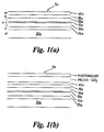
- a device body portion, generally designated 5a, from which the device is to be made includes at least one Quantum Well (QW) structure 10a.
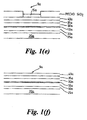
- the method includes the step of: causing an impurity material to intermix with the at least one Quantum Well 10a, wherein the impurity material includes Copper (Cu), see Figure 1(e).
- the impurity material substantially comprises Copper or an alloy thereof in this embodiment. It has been surprisingly found that Copper diffuses around 10 6 times faster than previously used impurities such as zinc (Zn).
- the method includes a preceding step of depositing on or adjacent the device body portion 5a a layer 15a including the impurity material.
- the impurity material is incorporated within a carrier material.
- the carrier material in this embodiment is a dielectric material such as Silica (SiO 2 ) or Aluminium Oxide (Al 2 O 3 ) .
- the layer 15a is deposited directly upon a surface of the device body portion 5a.
- the layer 15a is beneficially deposited by use of a diode or magnetron sputterer (not shown).
- the method begins with the step of providing a substrate 20 growing on the substrate 20a a first optical cladding layer 25a, a core guiding layer 30a including the at least one Quantum Well structure 10a, a second optical cladding layer 35a and optionally a contact layer 40a.
- the substrate 20a is typically doped n + while the first optical cladding layer 25a is doped n-type, the core guiding layer 30a being substantially intrinsic, the second optical cladding layer 35a being doped p-type and the contact layer 40a p + .
- first optical cladding layer 25a, core guiding layer 30a, second optically cladding layer 35a and contact layer 40a may be grown by any suitable growth technique such as Molecular Beam Epitaxy (MBE) or Metal Organic Vapour Deposition (MOCVD) .
- MBE Molecular Beam Epitaxy
- MOCVD Metal Organic Vapour Deposition
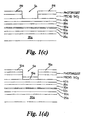
- the impurity material 15a is caused to intermix with the at least one Quantum Well 10a by raising the device body portion 5a to an elevated temperature for a predetermined time.
- the elevated temperature is in the region of 700°C - 950°C, while the predetermined time is in the region of 30 seconds to 300 seconds.
- the raising of the device body portion 5a to an elevated temperature in this embodiment comprises annealing of the device body portion 5a which causes diffusion of the Copper into the at least one Quantum Well 10a, and further out-diffusion of ions or atoms such as Gallium from the at least one Quantum Well 10a into the carrier material 15a.
- This embodiment therefore combines impurity induced and impurity free intermixing of the at least one Quantum Well 10a.
- the method of this first embodiment comprises the following steps:
- FIG. 2 there is illustrated a method of manufacturing an optical device according to a second embodiment of the present invention.
- This second embodiment differs from the first embodiment disclosed hereinbefore in that at the step of Figure 1(d) rather than depositing a single layer of material 15a including the intermixing material, a layer 15b comprising a layer of impurity material is deposited adjacent the surface of the device body portion 5b upon a spacer layer 16b.
- the spacer layer 16b conveniently comprises a dielectric material such as Silica (SiO 2 ) or Aluminium Oxide (Al 2 O 3 ).
- a further layer 17b eg. a further dielectric layer, is deposited on the layer 15a.
- the layer 15b is beneficially deposited by use of sputtering, and the spacer layer 16b and/or further layer 17b are beneficially deposited by use of sputtering or PECVD.
- FIG. 3 there is illustrated a method of manufacturing an optical device according to a third embodiment of the present invention.
- the method according to the third embodiment is similar to the method according to the first embodiment except that after the step Figure 1(d) the various layers including the layer 15c are removed from the device body portion 5c and a PECVD Silica layer is deposited on a surface of the device body portion 5c.
- the device body portion 5c is thereafter rapidly thermal annealed as in Figure 1(e). It has been surprisingly found that intermixing of the at least one Quantum Well 10c by the intermixing material (eg. Copper) still occurs in the embodiment of Figure 3 even though the layer 15c has been removed prior to rapid thermal annealing.
- the intermixing material eg. Copper
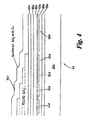
- FIG. 4 there is illustrated a sectional side view of a processing step involved in a method of manufacturing an optical device according to a fourth embodiment of the present invention.
- the device body portion 5d undergoes repeated patterning so as to provide a plurality of PECVD Silica layers so as to provide a stepped Silica pattern.
- the pattern including an exposed area of surface of the device body portion 5d without a PECVD Silica layer is shown in Figure 4.
- On top of the PECVD Silica layered pattern is deposited by sputtering a layer 15d, including the impurity material.
- the layer 15d comprises a carrier material such as Silica including an impurity material such as Copper.
- the device body portion 5d so patterned is then rapidly thermal annealed as shown in Figure 1(e) so as to provide a plurality of intermixed Quantum Well areas 45d, 50d, 55d, 60d, 65d within the device body portion 5d each intermixed Quantum Well area being tuned to a different band-gap since the intermixing induced by the Copper impurity material is different in each Quantum Well intermixed area since each Quantum Well intermixed area 45d to 65d is spaced by a different amount by the PECVD Silica stepped layers from the layer 15d.
- the impurity induced Quantum Well Intermixing methods or processes of the present invention may employ a Silica film doped with Cu to introduce a controlled amount of impurity into the semiconductor.
- Copper is a particularly effective impurity for impurity induced disordering. This is because Copper sits on both interstitial and substitutional sites and hops between them via the 'kick-out' mechanism. It possesses an extremely high diffusion coefficient, which means that intermixing takes place rapidly and, furthermore, the Copper diffuses rapidly leaving a low residual concentration in the intermixed layer.
- Copper can be introduced into the semiconductor by diffusion from a layer of Copper doped Silica.
- the layer is deposited using a diode or magnetron sputtering system and may be uniformly doped by simultaneously sputtering the Copper and SiO 2 (first embodiment) or the Copper may be incorporated in a single pure layer back-spaced from the semiconductor surface by a thin SiO 2 film (second embodiment).
- the latter approach appears to offer greater control over the level of Copper incorporation within the semiconductor.
- a thin layer (20-2000nm) of undoped Silica is deposited, followed by around 1-3 monolayers of Copper. The structure is then completed by a further deposition of undoped Silica.
- the sample is then annealed at temperatures in the range 700°C to 950°C for 30 to 300 s, depending on the material.
- Copper diffuses from the Silica layer into the semiconductor. Copper has an extremely high diffusion coefficient in the semiconductor, which means that intermixing takes place rapidly. Furthermore, the Copper diffuses rapidly into the device body leaving a low residual concentration in the intermixed layer.
- the epi-layers typically comprised an active region containing one or more Quantum Wells (QWs), generally 3-10 nm thick, within a higher band-gap waveguide core, 250-1000 nm thick which was surrounded by p-doped and n-doped cladding layers.
- QWs Quantum Wells
- the structures were all capped with a highly p-doped (1 x 10 29 cm -3 ) contact layer, typically 100-300 nm thick.
- the Copper was incorporated in a SiO 2 matrix, typically 200nm thick, by simultaneously sputtering both the Copper and the SiO 2 . This was achieved by reducing the height of the earth shield around the target so that part of the targets Copper backing plate was eroded.
- the degree of Quantum Well Intermixing induced by this process was determined by measuring the change in photoluminescence (PL) energy after annealing. In all cases this was compared against a control sample coated with PECVD SiO 2 , and all anneals were performed for 60 seconds unless otherwise stated.
- Figure 5 shows initial results obtained in MOVPE-grown InGaAs-InGaAsP emitting at 1550nm for samples capped with PECVD SiO 2 and sputtered Cu:SiO 2 . While samples capped with PECVD SiO 2 show initial band-gap shifts at temperatures of 650°C, significant band-gap shifts are obtained in Cu:SiO 2 capped material at temperatures approximately 100°C lower enabling differential band-gap shifts of 80 meV to be obtained at anneal temperatures of 650°C - 675°C.
- Band-gap shifts of similar magnitude were also obtained using sputtered Cu:SiO 2 films in GaAs-AlGaAs (850-860nm) and GaInP-AlGaInP (670nm) MQW structures, as shown in Figure 7.
- PECVD SiO 2 capped samples again yield negligible band-gap shifts over the temperature range used and for clarity are omitted from Figure 7. Over the same temperature range, negligible shifts were obtained for both materials when capped with PECVD SiO 2 .
- FIG. 9 shows band-gap shifts obtained in TnAlGaAs material for samples coated with both sputtered SiO 2 and Cu:SiO 2 , compared with samples coated with PECVD SiO 2 and undoped SiO 2 PECVD SiO 2 .
- Figure 11 illustrates SIMS profiles in InGaAsP MQW material capped with both PECVD SiO 2 and sputtered Cu:SiO 2 after a 680°C anneal. In and Ga out-diffusion is clearly observed for the sputter capped material but is not apparent in the PECVD SiO 2 cap.
- Figure 12 illustrates SIMS profile of an unannealed InAlGaAs MQW sample after removal of a sputtered Cu:SiO 2 coating.
- the Cu concentration rapidly decreases to the noise limit of 5 x 10 27 cm -3 at a depth of around 300nm.
- Figure 13 illustrates SIMS profile in InAlGaAs sample after annealing at 700°C and stripping of the Cu:SiO 2 cap.
- the sputtering of Cu:SiO 2 was performed in a first single target diode sputtering system using an Ar:O 2 (9:1) process gas and a sputtering pressure of 2x10 -3 mbar with an RF power of 110W, corresponding to a self dc bias of 1kV.
- the dependence of the Copper induced intermixing process on the sputtering conditions was investigated in the early stages of the process development. Some initial results suggested a near linear dependence of the shift upon film thickness, however there were a number of conflicting early reports and later studies showed that there was little dependence on the thickness of the sputtered layer. This appears consistent thickness of the sputtered layer.
- Figure 14 illustrates PL shifts obtained for InAlGaAs capped with PECVD SiO 2 sputtered SiO 2 and Cu:SiO 3 deposited in the second sputtering system and sputtered Cu:SiO 2 deposited in the first sputtering system.
- the degree of band-gap shift appeared to be slightly lower than that obtained in the first sputtering system, which may be explained by a slightly lower Copper incorporation level, probably caused by a reduced degree of exposure of the backing plate to the sputtering plasma.
- a third embodiment utilising a multi-layer approach is now described. As described earlier, this involves incorporating the Copper within a thin film close to the semiconductor surface, but backspaced from the surface by a thin layer of sputtered SiO 2 .
- the SiO 2 layers were sputtered using the standard conditions previously described, while the Copper layers were deposited at the same pressure but with a lower RF power of 25W to decrease the sputtering rate and provide greater control over the included Copper concentration.
- Figure 15 shows some typical results in InAlGaAs using this method, and particularly band-gap shifts achieved through a SiO 2 /Cu/SiO 2 multilayer deposition technique in InAlGaAs, where the second number refers to the deposition time for the Copper layer and the first and third values refer to the thicknesses of the surrounding SiO 2 layers.
- Figure 16 shows PL shifts in 980nm material when capped with PECVD SiO 2 and with sputtered SiO 2 /Cu/SiO 2 with varying thickness of the first SiO 2 layer thickness.
- the differential band-gap shift is largest for the layers in which the Copper is directly deposited onto the sample surface and decreases with increasing thickness of the SiO 2 backspacing layer.
- the degree to which the backspacing thickness can be increased is limited by the poor thermal stability of the material, which is turn limits the magnitude of the achievable differential band-gap shift.
- An increase in differential shift can be made simply by increasing the anneal times which can dramatically increase intermixing in the Copper doped films, while having little effect for PECVD SiO 2 layers.
Landscapes
- Chemical & Material Sciences (AREA)
- Nanotechnology (AREA)
- Engineering & Computer Science (AREA)
- Crystallography & Structural Chemistry (AREA)
- Optics & Photonics (AREA)
- Biophysics (AREA)
- Physics & Mathematics (AREA)
- Life Sciences & Earth Sciences (AREA)
- Semiconductor Lasers (AREA)
- Glass Compositions (AREA)
- Optical Couplings Of Light Guides (AREA)
- Optical Integrated Circuits (AREA)
- Physical Deposition Of Substances That Are Components Of Semiconductor Devices (AREA)
- Chemical Vapour Deposition (AREA)
Applications Claiming Priority (3)
| Application Number | Priority Date | Filing Date | Title |
|---|---|---|---|
| GB0122182A GB2379795B (en) | 2001-09-13 | 2001-09-13 | Method of manufacturing optical devices and related improvements |
| GB0122182 | 2001-09-13 | ||
| EP02751347A EP1425832B1 (de) | 2001-09-13 | 2002-07-30 | Verfahren zur herstellung optischer vorrichtungen und relatierten verbesserungen |
Related Parent Applications (1)
| Application Number | Title | Priority Date | Filing Date |
|---|---|---|---|
| EP02751347.2 Division | 2002-07-30 |
Publications (1)
| Publication Number | Publication Date |
|---|---|
| EP1598856A2 true EP1598856A2 (de) | 2005-11-23 |
Family
ID=9922049
Family Applications (2)
| Application Number | Title | Priority Date | Filing Date |
|---|---|---|---|
| EP02751347A Expired - Lifetime EP1425832B1 (de) | 2001-09-13 | 2002-07-30 | Verfahren zur herstellung optischer vorrichtungen und relatierten verbesserungen |
| EP05075513A Withdrawn EP1598856A2 (de) | 2001-09-13 | 2002-07-30 | Verfahren zur Herstellung optischer Vorrischtungen und relatierten Verbesserungen |
Family Applications Before (1)
| Application Number | Title | Priority Date | Filing Date |
|---|---|---|---|
| EP02751347A Expired - Lifetime EP1425832B1 (de) | 2001-09-13 | 2002-07-30 | Verfahren zur herstellung optischer vorrichtungen und relatierten verbesserungen |
Country Status (10)
| Country | Link |
|---|---|
| US (1) | US6719884B2 (de) |
| EP (2) | EP1425832B1 (de) |
| JP (1) | JP4711623B2 (de) |
| CN (2) | CN100461338C (de) |
| AT (1) | ATE544207T1 (de) |
| AU (1) | AU2002362238A1 (de) |
| CA (1) | CA2459763A1 (de) |
| GB (1) | GB2379795B (de) |
| RU (2) | RU2335035C2 (de) |
| WO (1) | WO2003023834A2 (de) |
Families Citing this family (14)
| Publication number | Priority date | Publication date | Assignee | Title |
|---|---|---|---|---|
| US7344905B2 (en) * | 2003-04-15 | 2008-03-18 | Ahura Corporation | Spatial bandgap modifications and energy shift of semiconductor structures |
| KR100577929B1 (ko) * | 2004-11-25 | 2006-05-10 | 한국전자통신연구원 | 도파로형 광 검출기 |
| US20070080455A1 (en) * | 2005-10-11 | 2007-04-12 | International Business Machines Corporation | Semiconductors and methods of making |
| US7863183B2 (en) * | 2006-01-18 | 2011-01-04 | International Business Machines Corporation | Method for fabricating last level copper-to-C4 connection with interfacial cap structure |
| TWI473209B (zh) * | 2009-12-09 | 2015-02-11 | Univ Nat Taiwan Science Tech | 電阻式記憶體的製造方法 |
| US9195007B2 (en) | 2012-06-28 | 2015-11-24 | Intel Corporation | Inverted 45 degree mirror for photonic integrated circuits |
| CN102916338B (zh) * | 2012-10-10 | 2018-11-02 | 长春理工大学 | 一种制作GaAs基半导体激光器非吸收窗口的方法 |
| RU2589759C1 (ru) * | 2015-03-10 | 2016-07-10 | Открытое акционерное общество "Центральный научно-исследовательский институт "ЦИКЛОН" | Фотоприемник на основе структуры с квантовыми ямами |
| RU2629891C1 (ru) * | 2016-04-29 | 2017-09-04 | Общество с ограниченной ответственностью "Малое инновационное предприятие "Пермские нанотехнологии" | Способ создания функциональных элементов интегральных оптических схем |
| CN111418120B (zh) * | 2017-12-04 | 2022-10-21 | 三菱电机株式会社 | 电场吸收型调制器、光半导体装置及光模块 |
| GB2572641B (en) | 2018-04-06 | 2021-06-02 | Rockley Photonics Ltd | Optoelectronic device and array thereof |
| RU190371U1 (ru) * | 2018-12-12 | 2019-06-28 | федеральное государственное автономное образовательное учреждение высшего образования "Национальный исследовательский ядерный университет "МИФИ" (НИЯУ МИФИ) | Полупроводниковая гетероструктура для интегрального оптического модулятора рефрактивного типа на подложке inp |
| US12294039B2 (en) * | 2019-09-20 | 2025-05-06 | Osram Opto Semiconductors Gmbh | Optoelectronic component, semiconductor structure and method |
| US12222448B1 (en) * | 2023-11-21 | 2025-02-11 | Aurora Operations, Inc. | LIDAR sensor system including integrated modulator |
Family Cites Families (29)
| Publication number | Priority date | Publication date | Assignee | Title |
|---|---|---|---|---|
| JPS54115088A (en) | 1978-02-28 | 1979-09-07 | Nec Corp | Double hetero junction laser element of stripe type |
| US4511408A (en) | 1982-04-22 | 1985-04-16 | The Board Of Trustees Of The University Of Illinois | Semiconductor device fabrication with disordering elements introduced into active region |
| US4639275A (en) | 1982-04-22 | 1987-01-27 | The Board Of Trustees Of The University Of Illinois | Forming disordered layer by controlled diffusion in heterojunction III-V semiconductor |
| US4594603A (en) | 1982-04-22 | 1986-06-10 | Board Of Trustees Of The University Of Illinois | Semiconductor device with disordered active region |
| US4585491A (en) | 1983-09-02 | 1986-04-29 | Xerox Corporation | Wavelength tuning of quantum well lasers by thermal annealing |
| JPS613488A (ja) * | 1984-06-15 | 1986-01-09 | Fujitsu Ltd | 半導体発光装置 |
| US4684653A (en) | 1985-03-08 | 1987-08-04 | The Trustees Of Princeton University | Pyrido(2,3-d)pyrimidine derivatives |
| US4727556A (en) | 1985-12-30 | 1988-02-23 | Xerox Corporation | Semiconductor lasers fabricated from impurity induced disordering |
| US4727557A (en) * | 1985-12-30 | 1988-02-23 | Xerox Corporation | Phased array semiconductor lasers fabricated from impurity induced disordering |
| US4871690A (en) | 1986-01-21 | 1989-10-03 | Xerox Corporation | Semiconductor structures utilizing semiconductor support means selectively pretreated with migratory defects |
| GB2198603A (en) | 1986-12-05 | 1988-06-15 | Philips Electronic Associated | Divider circuit |
| US4857971A (en) | 1987-03-23 | 1989-08-15 | Xerox Corporation | (IV)x (III-V)1-x alloys formed in situ in III-V heterostructures |
| JP2539416B2 (ja) * | 1987-03-25 | 1996-10-02 | 株式会社日立製作所 | 半導体レ−ザ装置 |
| US4990466A (en) | 1988-11-01 | 1991-02-05 | Siemens Corporate Research, Inc. | Method for fabricating index-guided semiconductor laser |
| US5238868A (en) | 1989-11-30 | 1993-08-24 | Gte Laboratories Incorporated | Bandgap tuning of semiconductor quantum well structures |
| RU2007788C1 (ru) * | 1991-04-30 | 1994-02-15 | Санкт-Петербургский технологический институт | Криогенный токоввод |
| US5384797A (en) | 1992-09-21 | 1995-01-24 | Sdl, Inc. | Monolithic multi-wavelength laser diode array |
| JPH06302906A (ja) * | 1993-04-12 | 1994-10-28 | Mitsubishi Electric Corp | 半導体レーザ及びその製造方法 |
| JPH07162086A (ja) * | 1993-12-10 | 1995-06-23 | Mitsubishi Electric Corp | 半導体レーザの製造方法 |
| US5395793A (en) | 1993-12-23 | 1995-03-07 | National Research Council Of Canada | Method of bandgap tuning of semiconductor quantum well structures |
| US5376583A (en) * | 1993-12-29 | 1994-12-27 | Xerox Corporation | Method for producing P-type impurity induced layer disordering |
| FR2715770B1 (fr) | 1994-01-31 | 1996-07-12 | France Telecom | Procédé pour la réalisation d'un composant électro-optique et/ou photonique. |
| US5708674A (en) * | 1995-01-03 | 1998-01-13 | Xerox Corporation | Semiconductor laser or array formed by layer intermixing |
| US5766981A (en) | 1995-01-04 | 1998-06-16 | Xerox Corporation | Thermally processed, phosphorus- or arsenic-containing semiconductor laser with selective IILD |
| GB9503981D0 (en) | 1995-02-28 | 1995-04-19 | Ca Nat Research Council | Bandag tuning of semiconductor well structures |
| JP2000138419A (ja) * | 1998-11-04 | 2000-05-16 | Hitachi Ltd | 半導体レーザ素子及びその製造方法 |
| JP2001135895A (ja) * | 1999-11-09 | 2001-05-18 | Mitsubishi Chemicals Corp | 半導体発光装置 |
| JP2001203423A (ja) * | 1999-11-09 | 2001-07-27 | Mitsubishi Chemicals Corp | 半導体発光装置 |
| CN1416589A (zh) * | 2000-03-08 | 2003-05-07 | Ntu企业私人有限公司 | 量子阱混合 |
-
2001
- 2001-09-13 GB GB0122182A patent/GB2379795B/en not_active Expired - Lifetime
-
2002
- 2002-01-15 US US10/047,308 patent/US6719884B2/en not_active Expired - Lifetime
- 2002-07-30 CN CNB2006100912258A patent/CN100461338C/zh not_active Expired - Fee Related
- 2002-07-30 JP JP2003527782A patent/JP4711623B2/ja not_active Expired - Fee Related
- 2002-07-30 EP EP02751347A patent/EP1425832B1/de not_active Expired - Lifetime
- 2002-07-30 WO PCT/GB2002/003464 patent/WO2003023834A2/en not_active Ceased
- 2002-07-30 AT AT02751347T patent/ATE544207T1/de active
- 2002-07-30 AU AU2002362238A patent/AU2002362238A1/en not_active Abandoned
- 2002-07-30 CA CA002459763A patent/CA2459763A1/en not_active Abandoned
- 2002-07-30 EP EP05075513A patent/EP1598856A2/de not_active Withdrawn
- 2002-07-30 CN CNB028180836A patent/CN1324774C/zh not_active Expired - Fee Related
- 2002-07-30 RU RU2004110997/28A patent/RU2335035C2/ru not_active IP Right Cessation
-
2008
- 2008-02-07 RU RU2008104790/28A patent/RU2008104790A/ru not_active Application Discontinuation
Also Published As
| Publication number | Publication date |
|---|---|
| ATE544207T1 (de) | 2012-02-15 |
| GB2379795B (en) | 2004-02-18 |
| GB2379795A8 (en) | 2003-10-16 |
| US20030053789A1 (en) | 2003-03-20 |
| RU2004110997A (ru) | 2005-03-27 |
| WO2003023834A3 (en) | 2004-01-08 |
| CA2459763A1 (en) | 2003-03-20 |
| AU2002362238A1 (en) | 2003-03-24 |
| GB0122182D0 (en) | 2001-10-31 |
| CN1324774C (zh) | 2007-07-04 |
| GB2379795A9 (en) | 2003-10-16 |
| GB2379795A (en) | 2003-03-19 |
| CN1555596A (zh) | 2004-12-15 |
| JP4711623B2 (ja) | 2011-06-29 |
| EP1425832A2 (de) | 2004-06-09 |
| EP1425832B1 (de) | 2012-02-01 |
| JP2005505125A (ja) | 2005-02-17 |
| CN1870220A (zh) | 2006-11-29 |
| US6719884B2 (en) | 2004-04-13 |
| WO2003023834A2 (en) | 2003-03-20 |
| RU2008104790A (ru) | 2009-08-20 |
| CN100461338C (zh) | 2009-02-11 |
| RU2335035C2 (ru) | 2008-09-27 |
Similar Documents
| Publication | Publication Date | Title |
|---|---|---|
| Kowalski et al. | A universal damage induced technique for quantum well intermixing | |
| EP1425832B1 (de) | Verfahren zur herstellung optischer vorrichtungen und relatierten verbesserungen | |
| KR20020089386A (ko) | 양자 우물 혼정 | |
| US6984538B2 (en) | Method for quantum well intermixing using pre-annealing enhanced defects diffusion | |
| KR101484354B1 (ko) | 양자 웰 혼합 방법 | |
| EP1368823B1 (de) | Herstellungsverfahren für optische vorrichtungen und verbesserungen | |
| US6632684B2 (en) | Method of manufacturing optical devices and related improvements | |
| JP4194844B2 (ja) | 複数の光学活性領域を備える半導体レーザ | |
| EP1364392B1 (de) | Herstellungsverfahren für optische vorrichtungen und verbesserungen | |
| US7151061B1 (en) | Method of selective post-growth tuning of an optical bandgap of a semi-conductor heterostructure and products produced thereof | |
| GB2385712A (en) | Optoelectronic devices | |
| Goldberg et al. | Ion beam intermixing of semiconductor heterostructures for optoelectronic applications | |
| Cusumano et al. | High extinction ratio GaAs/AlGaAs electroabsorption modulators integrated with passive waveguides using impurity-free vacancy diffusion | |
| ZA200205931B (en) | Quantum well intermixing. |
Legal Events
| Date | Code | Title | Description |
|---|---|---|---|
| PUAI | Public reference made under article 153(3) epc to a published international application that has entered the european phase |
Free format text: ORIGINAL CODE: 0009012 |
|
| 17P | Request for examination filed |
Effective date: 20050329 |
|
| AC | Divisional application: reference to earlier application |
Ref document number: 1425832 Country of ref document: EP Kind code of ref document: P |
|
| AK | Designated contracting states |
Kind code of ref document: A2 Designated state(s): AT BE BG CH CY CZ DE DK EE ES FI FR GB GR IE IT LI LU MC NL PT SE SK TR |
|
| RAP1 | Party data changed (applicant data changed or rights of an application transferred) |
Owner name: INTENSE LIMITED |
|
| STAA | Information on the status of an ep patent application or granted ep patent |
Free format text: STATUS: THE APPLICATION HAS BEEN WITHDRAWN |
|
| 18W | Application withdrawn |
Effective date: 20090814 |