EP1596428A1 - Organic thin-film transistor device and method for manufacturing same - Google Patents
Organic thin-film transistor device and method for manufacturing same Download PDFInfo
- Publication number
- EP1596428A1 EP1596428A1 EP04711711A EP04711711A EP1596428A1 EP 1596428 A1 EP1596428 A1 EP 1596428A1 EP 04711711 A EP04711711 A EP 04711711A EP 04711711 A EP04711711 A EP 04711711A EP 1596428 A1 EP1596428 A1 EP 1596428A1
- Authority
- EP
- European Patent Office
- Prior art keywords
- film transistor
- organic thin
- group
- film
- plasma
- Prior art date
- Legal status (The legal status is an assumption and is not a legal conclusion. Google has not performed a legal analysis and makes no representation as to the accuracy of the status listed.)
- Withdrawn
Links
- 238000000034 method Methods 0.000 title claims abstract description 129
- 239000010409 thin film Substances 0.000 title claims abstract description 73
- 238000004519 manufacturing process Methods 0.000 title claims abstract description 39
- 239000010408 film Substances 0.000 claims abstract description 63
- 239000004065 semiconductor Substances 0.000 claims abstract description 42
- 238000005229 chemical vapour deposition Methods 0.000 claims abstract description 24
- XLYOFNOQVPJJNP-UHFFFAOYSA-N water Substances O XLYOFNOQVPJJNP-UHFFFAOYSA-N 0.000 claims abstract description 16
- 239000007789 gas Substances 0.000 claims description 113
- -1 silane compound Chemical class 0.000 claims description 70
- 239000000758 substrate Substances 0.000 claims description 66
- 125000000217 alkyl group Chemical group 0.000 claims description 41
- 229910000077 silane Inorganic materials 0.000 claims description 16
- 229910052731 fluorine Inorganic materials 0.000 claims description 13
- 239000002994 raw material Substances 0.000 claims description 12
- 229920000642 polymer Polymers 0.000 claims description 11
- YCKRFDGAMUMZLT-UHFFFAOYSA-N Fluorine atom Chemical compound [F] YCKRFDGAMUMZLT-UHFFFAOYSA-N 0.000 claims description 10
- 239000011737 fluorine Substances 0.000 claims description 10
- 238000005268 plasma chemical vapour deposition Methods 0.000 claims description 10
- 229910052710 silicon Inorganic materials 0.000 claims description 10
- 229910052760 oxygen Inorganic materials 0.000 claims description 9
- QVGXLLKOCUKJST-UHFFFAOYSA-N atomic oxygen Chemical compound [O] QVGXLLKOCUKJST-UHFFFAOYSA-N 0.000 claims description 8
- 150000002894 organic compounds Chemical class 0.000 claims description 8
- 239000001301 oxygen Substances 0.000 claims description 8
- 150000003609 titanium compounds Chemical class 0.000 claims description 8
- 239000010703 silicon Substances 0.000 claims description 6
- 239000002904 solvent Substances 0.000 claims description 3
- 230000001747 exhibiting effect Effects 0.000 abstract description 4
- 208000028659 discharge Diseases 0.000 description 125
- 125000002023 trifluoromethyl group Chemical group FC(F)(F)* 0.000 description 62
- 150000001875 compounds Chemical class 0.000 description 41
- 239000000463 material Substances 0.000 description 35
- 125000001153 fluoro group Chemical group F* 0.000 description 33
- 239000000523 sample Substances 0.000 description 32
- OKTJSMMVPCPJKN-UHFFFAOYSA-N Carbon Chemical compound [C] OKTJSMMVPCPJKN-UHFFFAOYSA-N 0.000 description 22
- 125000002496 methyl group Chemical group [H]C([H])([H])* 0.000 description 20
- 229910052799 carbon Inorganic materials 0.000 description 19
- 125000003342 alkenyl group Chemical group 0.000 description 17
- IJGRMHOSHXDMSA-UHFFFAOYSA-N Atomic nitrogen Chemical compound N#N IJGRMHOSHXDMSA-UHFFFAOYSA-N 0.000 description 16
- 230000015572 biosynthetic process Effects 0.000 description 15
- 125000004435 hydrogen atom Chemical class [H]* 0.000 description 15
- 239000000243 solution Substances 0.000 description 15
- 229910052782 aluminium Inorganic materials 0.000 description 13
- VYPSYNLAJGMNEJ-UHFFFAOYSA-N Silicium dioxide Chemical compound O=[Si]=O VYPSYNLAJGMNEJ-UHFFFAOYSA-N 0.000 description 12
- XAGFODPZIPBFFR-UHFFFAOYSA-N aluminium Chemical compound [Al] XAGFODPZIPBFFR-UHFFFAOYSA-N 0.000 description 12
- 229910052814 silicon oxide Inorganic materials 0.000 description 12
- 229910052786 argon Inorganic materials 0.000 description 11
- 238000000576 coating method Methods 0.000 description 11
- 238000009832 plasma treatment Methods 0.000 description 11
- 229920005989 resin Polymers 0.000 description 11
- 239000011347 resin Substances 0.000 description 11
- 239000010936 titanium Substances 0.000 description 11
- 230000000694 effects Effects 0.000 description 10
- 229910052751 metal Inorganic materials 0.000 description 10
- 125000000962 organic group Chemical group 0.000 description 10
- YXFVVABEGXRONW-UHFFFAOYSA-N Toluene Chemical compound CC1=CC=CC=C1 YXFVVABEGXRONW-UHFFFAOYSA-N 0.000 description 9
- 239000002253 acid Substances 0.000 description 9
- 125000003545 alkoxy group Chemical group 0.000 description 9
- 239000002184 metal Substances 0.000 description 9
- 229910052757 nitrogen Inorganic materials 0.000 description 9
- CPUDPFPXCZDNGI-UHFFFAOYSA-N triethoxy(methyl)silane Chemical compound CCO[Si](C)(OCC)OCC CPUDPFPXCZDNGI-UHFFFAOYSA-N 0.000 description 9
- BLRPTPMANUNPDV-UHFFFAOYSA-N Silane Chemical compound [SiH4] BLRPTPMANUNPDV-UHFFFAOYSA-N 0.000 description 8
- 125000004429 atom Chemical group 0.000 description 8
- 230000000052 comparative effect Effects 0.000 description 8
- 239000011521 glass Substances 0.000 description 8
- 229910052809 inorganic oxide Inorganic materials 0.000 description 8
- 239000007788 liquid Substances 0.000 description 8
- 125000000956 methoxy group Chemical group [H]C([H])([H])O* 0.000 description 8
- 229910052719 titanium Inorganic materials 0.000 description 8
- RTAQQCXQSZGOHL-UHFFFAOYSA-N Titanium Chemical compound [Ti] RTAQQCXQSZGOHL-UHFFFAOYSA-N 0.000 description 7
- 125000001931 aliphatic group Chemical group 0.000 description 7
- 229910052734 helium Inorganic materials 0.000 description 7
- 239000000203 mixture Substances 0.000 description 7
- 150000002902 organometallic compounds Chemical class 0.000 description 7
- 239000007787 solid Substances 0.000 description 7
- XKRFYHLGVUSROY-UHFFFAOYSA-N Argon Chemical compound [Ar] XKRFYHLGVUSROY-UHFFFAOYSA-N 0.000 description 6
- HEDRZPFGACZZDS-UHFFFAOYSA-N Chloroform Chemical compound ClC(Cl)Cl HEDRZPFGACZZDS-UHFFFAOYSA-N 0.000 description 6
- FYYHWMGAXLPEAU-UHFFFAOYSA-N Magnesium Chemical compound [Mg] FYYHWMGAXLPEAU-UHFFFAOYSA-N 0.000 description 6
- 125000003302 alkenyloxy group Chemical group 0.000 description 6
- 239000003989 dielectric material Substances 0.000 description 6
- 229910001873 dinitrogen Inorganic materials 0.000 description 6
- 238000007599 discharging Methods 0.000 description 6
- 230000007062 hydrolysis Effects 0.000 description 6
- 238000006460 hydrolysis reaction Methods 0.000 description 6
- 239000011261 inert gas Substances 0.000 description 6
- 229910052749 magnesium Inorganic materials 0.000 description 6
- 239000011777 magnesium Substances 0.000 description 6
- 150000003961 organosilicon compounds Chemical class 0.000 description 6
- SLIUAWYAILUBJU-UHFFFAOYSA-N pentacene Chemical compound C1=CC=CC2=CC3=CC4=CC5=CC=CC=C5C=C4C=C3C=C21 SLIUAWYAILUBJU-UHFFFAOYSA-N 0.000 description 6
- BASFCYQUMIYNBI-UHFFFAOYSA-N platinum Chemical compound [Pt] BASFCYQUMIYNBI-UHFFFAOYSA-N 0.000 description 6
- 238000006467 substitution reaction Methods 0.000 description 6
- 238000004381 surface treatment Methods 0.000 description 6
- XEEYBQQBJWHFJM-UHFFFAOYSA-N Iron Chemical compound [Fe] XEEYBQQBJWHFJM-UHFFFAOYSA-N 0.000 description 5
- 229910052581 Si3N4 Inorganic materials 0.000 description 5
- BQCADISMDOOEFD-UHFFFAOYSA-N Silver Chemical compound [Ag] BQCADISMDOOEFD-UHFFFAOYSA-N 0.000 description 5
- GWEVSGVZZGPLCZ-UHFFFAOYSA-N Titan oxide Chemical compound O=[Ti]=O GWEVSGVZZGPLCZ-UHFFFAOYSA-N 0.000 description 5
- 125000001309 chloro group Chemical group Cl* 0.000 description 5
- 239000011248 coating agent Substances 0.000 description 5
- 239000010949 copper Substances 0.000 description 5
- 239000006185 dispersion Substances 0.000 description 5
- 238000001035 drying Methods 0.000 description 5
- 239000001307 helium Substances 0.000 description 5
- SWQJXJOGLNCZEY-UHFFFAOYSA-N helium atom Chemical compound [He] SWQJXJOGLNCZEY-UHFFFAOYSA-N 0.000 description 5
- 229910052740 iodine Inorganic materials 0.000 description 5
- TWNQGVIAIRXVLR-UHFFFAOYSA-N oxo(oxoalumanyloxy)alumane Chemical compound O=[Al]O[Al]=O TWNQGVIAIRXVLR-UHFFFAOYSA-N 0.000 description 5
- 125000005010 perfluoroalkyl group Chemical group 0.000 description 5
- 125000005009 perfluoropropyl group Chemical group FC(C(C(F)(F)F)(F)F)(F)* 0.000 description 5
- 125000001997 phenyl group Chemical group [H]C1=C([H])C([H])=C(*)C([H])=C1[H] 0.000 description 5
- 239000002243 precursor Substances 0.000 description 5
- 238000007639 printing Methods 0.000 description 5
- BBEAQIROQSPTKN-UHFFFAOYSA-N pyrene Chemical compound C1=CC=C2C=CC3=CC=CC4=CC=C1C2=C43 BBEAQIROQSPTKN-UHFFFAOYSA-N 0.000 description 5
- HQVNEWCFYHHQES-UHFFFAOYSA-N silicon nitride Chemical compound N12[Si]34N5[Si]62N3[Si]51N64 HQVNEWCFYHHQES-UHFFFAOYSA-N 0.000 description 5
- 229910052709 silver Inorganic materials 0.000 description 5
- 239000004332 silver Substances 0.000 description 5
- 238000004544 sputter deposition Methods 0.000 description 5
- 239000011135 tin Substances 0.000 description 5
- OGIDPMRJRNCKJF-UHFFFAOYSA-N titanium oxide Inorganic materials [Ti]=O OGIDPMRJRNCKJF-UHFFFAOYSA-N 0.000 description 5
- RYGMFSIKBFXOCR-UHFFFAOYSA-N Copper Chemical compound [Cu] RYGMFSIKBFXOCR-UHFFFAOYSA-N 0.000 description 4
- MHAJPDPJQMAIIY-UHFFFAOYSA-N Hydrogen peroxide Chemical compound OO MHAJPDPJQMAIIY-UHFFFAOYSA-N 0.000 description 4
- UFWIBTONFRDIAS-UHFFFAOYSA-N Naphthalene Chemical compound C1=CC=CC2=CC=CC=C21 UFWIBTONFRDIAS-UHFFFAOYSA-N 0.000 description 4
- XUIMIQQOPSSXEZ-UHFFFAOYSA-N Silicon Chemical compound [Si] XUIMIQQOPSSXEZ-UHFFFAOYSA-N 0.000 description 4
- WYURNTSHIVDZCO-UHFFFAOYSA-N Tetrahydrofuran Chemical compound C1CCOC1 WYURNTSHIVDZCO-UHFFFAOYSA-N 0.000 description 4
- YTPLMLYBLZKORZ-UHFFFAOYSA-N Thiophene Chemical compound C=1C=CSC=1 YTPLMLYBLZKORZ-UHFFFAOYSA-N 0.000 description 4
- 229910010062 TiCl3 Inorganic materials 0.000 description 4
- VNSWULZVUKFJHK-UHFFFAOYSA-N [Sr].[Bi] Chemical compound [Sr].[Bi] VNSWULZVUKFJHK-UHFFFAOYSA-N 0.000 description 4
- MWPLVEDNUUSJAV-UHFFFAOYSA-N anthracene Chemical compound C1=CC=CC2=CC3=CC=CC=C3C=C21 MWPLVEDNUUSJAV-UHFFFAOYSA-N 0.000 description 4
- 229910002115 bismuth titanate Inorganic materials 0.000 description 4
- 239000003990 capacitor Substances 0.000 description 4
- 229910052801 chlorine Inorganic materials 0.000 description 4
- 229920001577 copolymer Polymers 0.000 description 4
- 229910052802 copper Inorganic materials 0.000 description 4
- 239000002019 doping agent Substances 0.000 description 4
- 230000005684 electric field Effects 0.000 description 4
- 125000000524 functional group Chemical group 0.000 description 4
- 125000005843 halogen group Chemical group 0.000 description 4
- 150000002430 hydrocarbons Chemical group 0.000 description 4
- 229910052738 indium Inorganic materials 0.000 description 4
- 150000004767 nitrides Chemical class 0.000 description 4
- BPUBBGLMJRNUCC-UHFFFAOYSA-N oxygen(2-);tantalum(5+) Chemical compound [O-2].[O-2].[O-2].[O-2].[O-2].[Ta+5].[Ta+5] BPUBBGLMJRNUCC-UHFFFAOYSA-N 0.000 description 4
- 125000005007 perfluorooctyl group Chemical group FC(C(C(C(C(C(C(C(F)(F)F)(F)F)(F)F)(F)F)(F)F)(F)F)(F)F)(F)* 0.000 description 4
- 229920006395 saturated elastomer Polymers 0.000 description 4
- 238000005507 spraying Methods 0.000 description 4
- 229910001220 stainless steel Inorganic materials 0.000 description 4
- 239000010935 stainless steel Substances 0.000 description 4
- 229910001936 tantalum oxide Inorganic materials 0.000 description 4
- 238000005406 washing Methods 0.000 description 4
- ZWEHNKRNPOVVGH-UHFFFAOYSA-N 2-Butanone Chemical compound CCC(C)=O ZWEHNKRNPOVVGH-UHFFFAOYSA-N 0.000 description 3
- TXBCBTDQIULDIA-UHFFFAOYSA-N 2-[[3-hydroxy-2,2-bis(hydroxymethyl)propoxy]methyl]-2-(hydroxymethyl)propane-1,3-diol Chemical compound OCC(CO)(CO)COCC(CO)(CO)CO TXBCBTDQIULDIA-UHFFFAOYSA-N 0.000 description 3
- 125000000954 2-hydroxyethyl group Chemical group [H]C([*])([H])C([H])([H])O[H] 0.000 description 3
- ZCYVEMRRCGMTRW-UHFFFAOYSA-N 7553-56-2 Chemical group [I] ZCYVEMRRCGMTRW-UHFFFAOYSA-N 0.000 description 3
- WKBOTKDWSSQWDR-UHFFFAOYSA-N Bromine atom Chemical group [Br] WKBOTKDWSSQWDR-UHFFFAOYSA-N 0.000 description 3
- TYJFMLFZOHGQOA-UHFFFAOYSA-N CC(C)O[Ti](C)(OC(C)C)OC(C)C Chemical compound CC(C)O[Ti](C)(OC(C)C)OC(C)C TYJFMLFZOHGQOA-UHFFFAOYSA-N 0.000 description 3
- UJOBWOGCFQCDNV-UHFFFAOYSA-N Carbazole Natural products C1=CC=C2C3=CC=CC=C3NC2=C1 UJOBWOGCFQCDNV-UHFFFAOYSA-N 0.000 description 3
- VOPWNXZWBYDODV-UHFFFAOYSA-N Chlorodifluoromethane Chemical compound FC(F)Cl VOPWNXZWBYDODV-UHFFFAOYSA-N 0.000 description 3
- YMWUJEATGCHHMB-UHFFFAOYSA-N Dichloromethane Chemical compound ClCCl YMWUJEATGCHHMB-UHFFFAOYSA-N 0.000 description 3
- XEKOWRVHYACXOJ-UHFFFAOYSA-N Ethyl acetate Chemical compound CCOC(C)=O XEKOWRVHYACXOJ-UHFFFAOYSA-N 0.000 description 3
- UFHFLCQGNIYNRP-UHFFFAOYSA-N Hydrogen Chemical compound [H][H] UFHFLCQGNIYNRP-UHFFFAOYSA-N 0.000 description 3
- WHXSMMKQMYFTQS-UHFFFAOYSA-N Lithium Chemical compound [Li] WHXSMMKQMYFTQS-UHFFFAOYSA-N 0.000 description 3
- PXHVJJICTQNCMI-UHFFFAOYSA-N Nickel Chemical compound [Ni] PXHVJJICTQNCMI-UHFFFAOYSA-N 0.000 description 3
- 239000006087 Silane Coupling Agent Substances 0.000 description 3
- 125000003277 amino group Chemical group 0.000 description 3
- 238000007611 bar coating method Methods 0.000 description 3
- 125000004432 carbon atom Chemical group C* 0.000 description 3
- 239000000919 ceramic Substances 0.000 description 3
- 238000006243 chemical reaction Methods 0.000 description 3
- 229920001940 conductive polymer Polymers 0.000 description 3
- 239000004020 conductor Substances 0.000 description 3
- 238000001816 cooling Methods 0.000 description 3
- 125000000753 cycloalkyl group Chemical group 0.000 description 3
- 238000007607 die coating method Methods 0.000 description 3
- GKDMBSRWOMWLBC-UHFFFAOYSA-N diethoxy-ethyl-(1,1,1-trifluoropropan-2-yloxy)silane Chemical compound CCO[Si](CC)(OCC)OC(C)C(F)(F)F GKDMBSRWOMWLBC-UHFFFAOYSA-N 0.000 description 3
- 238000003618 dip coating Methods 0.000 description 3
- 238000005516 engineering process Methods 0.000 description 3
- GVEPBJHOBDJJJI-UHFFFAOYSA-N fluoranthrene Natural products C1=CC(C2=CC=CC=C22)=C3C2=CC=CC3=C1 GVEPBJHOBDJJJI-UHFFFAOYSA-N 0.000 description 3
- 229910052732 germanium Inorganic materials 0.000 description 3
- 238000010438 heat treatment Methods 0.000 description 3
- 239000001257 hydrogen Substances 0.000 description 3
- 229910052739 hydrogen Inorganic materials 0.000 description 3
- 125000002887 hydroxy group Chemical group [H]O* 0.000 description 3
- APFVFJFRJDLVQX-UHFFFAOYSA-N indium atom Chemical compound [In] APFVFJFRJDLVQX-UHFFFAOYSA-N 0.000 description 3
- GRPQBOKWXNIQMF-UHFFFAOYSA-N indium(3+) oxygen(2-) tin(4+) Chemical compound [Sn+4].[O-2].[In+3] GRPQBOKWXNIQMF-UHFFFAOYSA-N 0.000 description 3
- 229910010272 inorganic material Inorganic materials 0.000 description 3
- 229910052746 lanthanum Inorganic materials 0.000 description 3
- 239000004973 liquid crystal related substance Substances 0.000 description 3
- 229910052744 lithium Inorganic materials 0.000 description 3
- 230000010355 oscillation Effects 0.000 description 3
- 239000002245 particle Substances 0.000 description 3
- 238000000059 patterning Methods 0.000 description 3
- 238000000206 photolithography Methods 0.000 description 3
- 229910052697 platinum Inorganic materials 0.000 description 3
- 229920000301 poly(3-hexylthiophene-2,5-diyl) polymer Polymers 0.000 description 3
- 229920000767 polyaniline Polymers 0.000 description 3
- 239000005020 polyethylene terephthalate Substances 0.000 description 3
- 229920001721 polyimide Polymers 0.000 description 3
- 238000006116 polymerization reaction Methods 0.000 description 3
- 229920000128 polypyrrole Polymers 0.000 description 3
- 229920000123 polythiophene Polymers 0.000 description 3
- 238000004528 spin coating Methods 0.000 description 3
- 229910052717 sulfur Inorganic materials 0.000 description 3
- 230000003746 surface roughness Effects 0.000 description 3
- FHCPAXDKURNIOZ-UHFFFAOYSA-N tetrathiafulvalene Chemical compound S1C=CSC1=C1SC=CS1 FHCPAXDKURNIOZ-UHFFFAOYSA-N 0.000 description 3
- WUMSTCDLAYQDNO-UHFFFAOYSA-N triethoxy(hexyl)silane Chemical compound CCCCCC[Si](OCC)(OCC)OCC WUMSTCDLAYQDNO-UHFFFAOYSA-N 0.000 description 3
- 238000001771 vacuum deposition Methods 0.000 description 3
- 229910052725 zinc Inorganic materials 0.000 description 3
- 239000011701 zinc Substances 0.000 description 3
- FKTXDTWDCPTPHK-UHFFFAOYSA-N 1,1,1,2,3,3,3-heptafluoropropane Chemical compound FC(F)(F)[C](F)C(F)(F)F FKTXDTWDCPTPHK-UHFFFAOYSA-N 0.000 description 2
- DXBHBZVCASKNBY-UHFFFAOYSA-N 1,2-Benz(a)anthracene Chemical compound C1=CC=C2C3=CC4=CC=CC=C4C=C3C=CC2=C1 DXBHBZVCASKNBY-UHFFFAOYSA-N 0.000 description 2
- MFEVGQHCNVXMER-UHFFFAOYSA-L 1,3,2$l^{2}-dioxaplumbetan-4-one Chemical compound [Pb+2].[O-]C([O-])=O MFEVGQHCNVXMER-UHFFFAOYSA-L 0.000 description 2
- 229920003026 Acene Polymers 0.000 description 2
- DLFVBJFMPXGRIB-UHFFFAOYSA-N Acetamide Chemical compound CC(N)=O DLFVBJFMPXGRIB-UHFFFAOYSA-N 0.000 description 2
- XMWRBQBLMFGWIX-UHFFFAOYSA-N C60 fullerene Chemical class C12=C3C(C4=C56)=C7C8=C5C5=C9C%10=C6C6=C4C1=C1C4=C6C6=C%10C%10=C9C9=C%11C5=C8C5=C8C7=C3C3=C7C2=C1C1=C2C4=C6C4=C%10C6=C9C9=C%11C5=C5C8=C3C3=C7C1=C1C2=C4C6=C2C9=C5C3=C12 XMWRBQBLMFGWIX-UHFFFAOYSA-N 0.000 description 2
- 239000004215 Carbon black (E152) Substances 0.000 description 2
- CURLTUGMZLYLDI-UHFFFAOYSA-N Carbon dioxide Chemical compound O=C=O CURLTUGMZLYLDI-UHFFFAOYSA-N 0.000 description 2
- 229920008347 Cellulose acetate propionate Polymers 0.000 description 2
- RTZKZFJDLAIYFH-UHFFFAOYSA-N Diethyl ether Chemical compound CCOCC RTZKZFJDLAIYFH-UHFFFAOYSA-N 0.000 description 2
- DGAQECJNVWCQMB-PUAWFVPOSA-M Ilexoside XXIX Chemical compound C[C@@H]1CC[C@@]2(CC[C@@]3(C(=CC[C@H]4[C@]3(CC[C@@H]5[C@@]4(CC[C@@H](C5(C)C)OS(=O)(=O)[O-])C)C)[C@@H]2[C@]1(C)O)C)C(=O)O[C@H]6[C@@H]([C@H]([C@@H]([C@H](O6)CO)O)O)O.[Na+] DGAQECJNVWCQMB-PUAWFVPOSA-M 0.000 description 2
- 229910000003 Lead carbonate Inorganic materials 0.000 description 2
- CBENFWSGALASAD-UHFFFAOYSA-N Ozone Chemical compound [O-][O+]=O CBENFWSGALASAD-UHFFFAOYSA-N 0.000 description 2
- KDLHZDBZIXYQEI-UHFFFAOYSA-N Palladium Chemical compound [Pd] KDLHZDBZIXYQEI-UHFFFAOYSA-N 0.000 description 2
- 229920001609 Poly(3,4-ethylenedioxythiophene) Polymers 0.000 description 2
- 239000004642 Polyimide Substances 0.000 description 2
- 239000004734 Polyphenylene sulfide Substances 0.000 description 2
- 239000004372 Polyvinyl alcohol Substances 0.000 description 2
- 229910002808 Si–O–Si Inorganic materials 0.000 description 2
- NINIDFKCEFEMDL-UHFFFAOYSA-N Sulfur Chemical compound [S] NINIDFKCEFEMDL-UHFFFAOYSA-N 0.000 description 2
- BOTDANWDWHJENH-UHFFFAOYSA-N Tetraethyl orthosilicate Chemical compound CCO[Si](OCC)(OCC)OCC BOTDANWDWHJENH-UHFFFAOYSA-N 0.000 description 2
- DTQVDTLACAAQTR-UHFFFAOYSA-N Trifluoroacetic acid Chemical compound OC(=O)C(F)(F)F DTQVDTLACAAQTR-UHFFFAOYSA-N 0.000 description 2
- 229920002433 Vinyl chloride-vinyl acetate copolymer Polymers 0.000 description 2
- XLOMVQKBTHCTTD-UHFFFAOYSA-N Zinc monoxide Chemical compound [Zn]=O XLOMVQKBTHCTTD-UHFFFAOYSA-N 0.000 description 2
- XHCLAFWTIXFWPH-UHFFFAOYSA-N [O-2].[O-2].[O-2].[O-2].[O-2].[V+5].[V+5] Chemical compound [O-2].[O-2].[O-2].[O-2].[O-2].[V+5].[V+5] XHCLAFWTIXFWPH-UHFFFAOYSA-N 0.000 description 2
- 125000005370 alkoxysilyl group Chemical group 0.000 description 2
- 125000005103 alkyl silyl group Chemical group 0.000 description 2
- 125000001118 alkylidene group Chemical group 0.000 description 2
- 229910021417 amorphous silicon Inorganic materials 0.000 description 2
- 229910052787 antimony Inorganic materials 0.000 description 2
- 125000002029 aromatic hydrocarbon group Chemical group 0.000 description 2
- 239000012298 atmosphere Substances 0.000 description 2
- 229910052454 barium strontium titanate Inorganic materials 0.000 description 2
- JRPBQTZRNDNNOP-UHFFFAOYSA-N barium titanate Chemical compound [Ba+2].[Ba+2].[O-][Ti]([O-])([O-])[O-] JRPBQTZRNDNNOP-UHFFFAOYSA-N 0.000 description 2
- 229910002113 barium titanate Inorganic materials 0.000 description 2
- 229910021523 barium zirconate Inorganic materials 0.000 description 2
- DQBAOWPVHRWLJC-UHFFFAOYSA-N barium(2+);dioxido(oxo)zirconium Chemical compound [Ba+2].[O-][Zr]([O-])=O DQBAOWPVHRWLJC-UHFFFAOYSA-N 0.000 description 2
- 229910052797 bismuth Inorganic materials 0.000 description 2
- JCXGWMGPZLAOME-UHFFFAOYSA-N bismuth atom Chemical compound [Bi] JCXGWMGPZLAOME-UHFFFAOYSA-N 0.000 description 2
- 239000005385 borate glass Substances 0.000 description 2
- 125000002915 carbonyl group Chemical group [*:2]C([*:1])=O 0.000 description 2
- 238000005266 casting Methods 0.000 description 2
- 239000003153 chemical reaction reagent Substances 0.000 description 2
- 239000000460 chlorine Substances 0.000 description 2
- MVPPADPHJFYWMZ-UHFFFAOYSA-N chlorobenzene Chemical compound ClC1=CC=CC=C1 MVPPADPHJFYWMZ-UHFFFAOYSA-N 0.000 description 2
- WDECIBYCCFPHNR-UHFFFAOYSA-N chrysene Chemical compound C1=CC=CC2=CC=C3C4=CC=CC=C4C=CC3=C21 WDECIBYCCFPHNR-UHFFFAOYSA-N 0.000 description 2
- PMHQVHHXPFUNSP-UHFFFAOYSA-M copper(1+);methylsulfanylmethane;bromide Chemical compound Br[Cu].CSC PMHQVHHXPFUNSP-UHFFFAOYSA-M 0.000 description 2
- VPUGDVKSAQVFFS-UHFFFAOYSA-N coronene Chemical compound C1=C(C2=C34)C=CC3=CC=C(C=C3)C4=C4C3=CC=C(C=C3)C4=C2C3=C1 VPUGDVKSAQVFFS-UHFFFAOYSA-N 0.000 description 2
- RAABOESOVLLHRU-UHFFFAOYSA-N diazene Chemical compound N=N RAABOESOVLLHRU-UHFFFAOYSA-N 0.000 description 2
- 229910000071 diazene Inorganic materials 0.000 description 2
- RWRIWBAIICGTTQ-UHFFFAOYSA-N difluoromethane Chemical compound FCF RWRIWBAIICGTTQ-UHFFFAOYSA-N 0.000 description 2
- JJQZDUKDJDQPMQ-UHFFFAOYSA-N dimethoxy(dimethyl)silane Chemical compound CO[Si](C)(C)OC JJQZDUKDJDQPMQ-UHFFFAOYSA-N 0.000 description 2
- YYLGKUPAFFKGRQ-UHFFFAOYSA-N dimethyldiethoxysilane Chemical compound CCO[Si](C)(C)OCC YYLGKUPAFFKGRQ-UHFFFAOYSA-N 0.000 description 2
- UBHZUDXTHNMNLD-UHFFFAOYSA-N dimethylsilane Chemical compound C[SiH2]C UBHZUDXTHNMNLD-UHFFFAOYSA-N 0.000 description 2
- 238000001962 electrophoresis Methods 0.000 description 2
- RSIHJDGMBDPTIM-UHFFFAOYSA-N ethoxy(trimethyl)silane Chemical compound CCO[Si](C)(C)C RSIHJDGMBDPTIM-UHFFFAOYSA-N 0.000 description 2
- 230000005669 field effect Effects 0.000 description 2
- 229910003472 fullerene Inorganic materials 0.000 description 2
- PCHJSUWPFVWCPO-UHFFFAOYSA-N gold Chemical compound [Au] PCHJSUWPFVWCPO-UHFFFAOYSA-N 0.000 description 2
- 229910052737 gold Inorganic materials 0.000 description 2
- 239000010931 gold Substances 0.000 description 2
- 125000006343 heptafluoro propyl group Chemical group 0.000 description 2
- 229930195733 hydrocarbon Natural products 0.000 description 2
- 239000011147 inorganic material Substances 0.000 description 2
- 238000009413 insulation Methods 0.000 description 2
- 239000011630 iodine Substances 0.000 description 2
- 238000007733 ion plating Methods 0.000 description 2
- 238000010884 ion-beam technique Methods 0.000 description 2
- 150000002500 ions Chemical class 0.000 description 2
- 229910052742 iron Inorganic materials 0.000 description 2
- IQPQWNKOIGAROB-UHFFFAOYSA-N isocyanate group Chemical group [N-]=C=O IQPQWNKOIGAROB-UHFFFAOYSA-N 0.000 description 2
- FZLIPJUXYLNCLC-UHFFFAOYSA-N lanthanum atom Chemical compound [La] FZLIPJUXYLNCLC-UHFFFAOYSA-N 0.000 description 2
- COQAIRYMVBNUKQ-UHFFFAOYSA-J magnesium;barium(2+);tetrafluoride Chemical compound [F-].[F-].[F-].[F-].[Mg+2].[Ba+2] COQAIRYMVBNUKQ-UHFFFAOYSA-J 0.000 description 2
- 229910044991 metal oxide Inorganic materials 0.000 description 2
- QLOAVXSYZAJECW-UHFFFAOYSA-N methane;molecular fluorine Chemical compound C.FF QLOAVXSYZAJECW-UHFFFAOYSA-N 0.000 description 2
- 239000002052 molecular layer Substances 0.000 description 2
- 229910052759 nickel Inorganic materials 0.000 description 2
- 239000003960 organic solvent Substances 0.000 description 2
- RUDFQVOCFDJEEF-UHFFFAOYSA-N oxygen(2-);yttrium(3+) Chemical compound [O-2].[O-2].[O-2].[Y+3].[Y+3] RUDFQVOCFDJEEF-UHFFFAOYSA-N 0.000 description 2
- NFHFRUOZVGFOOS-UHFFFAOYSA-N palladium;triphenylphosphane Chemical compound [Pd].C1=CC=CC=C1P(C=1C=CC=CC=1)C1=CC=CC=C1.C1=CC=CC=C1P(C=1C=CC=CC=1)C1=CC=CC=C1.C1=CC=CC=C1P(C=1C=CC=CC=1)C1=CC=CC=C1.C1=CC=CC=C1P(C=1C=CC=CC=1)C1=CC=CC=C1 NFHFRUOZVGFOOS-UHFFFAOYSA-N 0.000 description 2
- 125000006340 pentafluoro ethyl group Chemical group FC(F)(F)C(F)(F)* 0.000 description 2
- 125000005004 perfluoroethyl group Chemical group FC(F)(F)C(F)(F)* 0.000 description 2
- 239000002985 plastic film Substances 0.000 description 2
- 229920000172 poly(styrenesulfonic acid) Polymers 0.000 description 2
- 229920001197 polyacetylene Polymers 0.000 description 2
- 229920000323 polyazulene Polymers 0.000 description 2
- 229920001088 polycarbazole Polymers 0.000 description 2
- 229910021420 polycrystalline silicon Inorganic materials 0.000 description 2
- 229920000139 polyethylene terephthalate Polymers 0.000 description 2
- 229920000414 polyfuran Polymers 0.000 description 2
- 229920000069 polyphenylene sulfide Polymers 0.000 description 2
- 229940005642 polystyrene sulfonic acid Drugs 0.000 description 2
- 229920002451 polyvinyl alcohol Polymers 0.000 description 2
- 230000009257 reactivity Effects 0.000 description 2
- 125000003808 silyl group Chemical group [H][Si]([H])([H])[*] 0.000 description 2
- 229910052708 sodium Inorganic materials 0.000 description 2
- 239000011734 sodium Substances 0.000 description 2
- VEALVRVVWBQVSL-UHFFFAOYSA-N strontium titanate Chemical compound [Sr+2].[O-][Ti]([O-])=O VEALVRVVWBQVSL-UHFFFAOYSA-N 0.000 description 2
- 239000000126 substance Substances 0.000 description 2
- 239000011593 sulfur Substances 0.000 description 2
- 239000004094 surface-active agent Substances 0.000 description 2
- 238000010408 sweeping Methods 0.000 description 2
- YLQBMQCUIZJEEH-UHFFFAOYSA-N tetrahydrofuran Natural products C=1C=COC=1 YLQBMQCUIZJEEH-UHFFFAOYSA-N 0.000 description 2
- LFQCEHFDDXELDD-UHFFFAOYSA-N tetramethyl orthosilicate Chemical compound CO[Si](OC)(OC)OC LFQCEHFDDXELDD-UHFFFAOYSA-N 0.000 description 2
- 229930192474 thiophene Natural products 0.000 description 2
- 229910052718 tin Inorganic materials 0.000 description 2
- XOLBLPGZBRYERU-UHFFFAOYSA-N tin dioxide Chemical compound O=[Sn]=O XOLBLPGZBRYERU-UHFFFAOYSA-N 0.000 description 2
- 229910001887 tin oxide Inorganic materials 0.000 description 2
- DENFJSAFJTVPJR-UHFFFAOYSA-N triethoxy(ethyl)silane Chemical compound CCO[Si](CC)(OCC)OCC DENFJSAFJTVPJR-UHFFFAOYSA-N 0.000 description 2
- 125000000876 trifluoromethoxy group Chemical group FC(F)(F)O* 0.000 description 2
- 239000013638 trimer Substances 0.000 description 2
- DBUFXGVMAMMWSD-UHFFFAOYSA-N trimethoxy-[3-(7-oxabicyclo[4.1.0]heptan-4-yl)propyl]silane Chemical compound C1C(CCC[Si](OC)(OC)OC)CCC2OC21 DBUFXGVMAMMWSD-UHFFFAOYSA-N 0.000 description 2
- 229910001935 vanadium oxide Inorganic materials 0.000 description 2
- 230000003245 working effect Effects 0.000 description 2
- 229910052726 zirconium Inorganic materials 0.000 description 2
- NLELYIIJDKQXTL-UHFFFAOYSA-N (2,3-diethoxyphenyl)-phenylmethanone Chemical compound CCOC1=CC=CC(C(=O)C=2C=CC=CC=2)=C1OCC NLELYIIJDKQXTL-UHFFFAOYSA-N 0.000 description 1
- WYTZZXDRDKSJID-UHFFFAOYSA-N (3-aminopropyl)triethoxysilane Chemical compound CCO[Si](OCC)(OCC)CCCN WYTZZXDRDKSJID-UHFFFAOYSA-N 0.000 description 1
- LVGUZGTVOIAKKC-UHFFFAOYSA-N 1,1,1,2-tetrafluoroethane Chemical compound FCC(F)(F)F LVGUZGTVOIAKKC-UHFFFAOYSA-N 0.000 description 1
- KQUZDBCORBKBQL-UHFFFAOYSA-N 1,1,1,5,5-pentafluoropentan-3-one Chemical compound FC(CC(=O)CC(F)(F)F)F KQUZDBCORBKBQL-UHFFFAOYSA-N 0.000 description 1
- COLOHWPRNRVWPI-UHFFFAOYSA-N 1,1,1-trifluoroethane Chemical compound [CH2]C(F)(F)F COLOHWPRNRVWPI-UHFFFAOYSA-N 0.000 description 1
- NNZZMYIWZFZLHU-UHFFFAOYSA-N 1,1,2,2,2-pentafluoroethanol Chemical compound OC(F)(F)C(F)(F)F NNZZMYIWZFZLHU-UHFFFAOYSA-N 0.000 description 1
- XWKHVYYVLSSVEW-UHFFFAOYSA-N 1,1,2,2,3,3,3-heptafluoropropoxy(dimethyl)silane Chemical compound FC(C(C(F)(F)F)(F)F)(O[SiH](C)C)F XWKHVYYVLSSVEW-UHFFFAOYSA-N 0.000 description 1
- SCYULBFZEHDVBN-UHFFFAOYSA-N 1,1-Dichloroethane Chemical compound CC(Cl)Cl SCYULBFZEHDVBN-UHFFFAOYSA-N 0.000 description 1
- GEYOCULIXLDCMW-UHFFFAOYSA-N 1,2-phenylenediamine Chemical compound NC1=CC=CC=C1N GEYOCULIXLDCMW-UHFFFAOYSA-N 0.000 description 1
- YJTKZCDBKVTVBY-UHFFFAOYSA-N 1,3-Diphenylbenzene Chemical group C1=CC=CC=C1C1=CC=CC(C=2C=CC=CC=2)=C1 YJTKZCDBKVTVBY-UHFFFAOYSA-N 0.000 description 1
- 150000004057 1,4-benzoquinones Chemical class 0.000 description 1
- OYIDEQGUYHKUQY-UHFFFAOYSA-N 2,2-dibutoxyethoxy-methyl-[3-(oxiran-2-ylmethoxy)propyl]silane Chemical compound CCCCOC(CO[SiH](C)CCCOCC1CO1)OCCCC OYIDEQGUYHKUQY-UHFFFAOYSA-N 0.000 description 1
- AHFXIFMCZUNFSI-UHFFFAOYSA-N 2,2-dimethoxyethoxy-methyl-[3-(oxiran-2-ylmethoxy)propyl]silane Chemical compound COC(CO[SiH](C)CCCOCC1CO1)OC AHFXIFMCZUNFSI-UHFFFAOYSA-N 0.000 description 1
- SMZOUWXMTYCWNB-UHFFFAOYSA-N 2-(2-methoxy-5-methylphenyl)ethanamine Chemical compound COC1=CC=C(C)C=C1CCN SMZOUWXMTYCWNB-UHFFFAOYSA-N 0.000 description 1
- ORDZXCQDZLMHAM-UHFFFAOYSA-N 2-(7-oxabicyclo[4.1.0]heptan-4-yl)ethyl-triphenoxysilane Chemical compound C1CC2OC2CC1CC[Si](OC=1C=CC=CC=1)(OC=1C=CC=CC=1)OC1=CC=CC=C1 ORDZXCQDZLMHAM-UHFFFAOYSA-N 0.000 description 1
- ROYZOPPLNMOKCU-UHFFFAOYSA-N 2-(7-oxabicyclo[4.1.0]heptan-4-yl)ethyl-tripropoxysilane Chemical compound C1C(CC[Si](OCCC)(OCCC)OCCC)CCC2OC21 ROYZOPPLNMOKCU-UHFFFAOYSA-N 0.000 description 1
- NIXOWILDQLNWCW-UHFFFAOYSA-N 2-Propenoic acid Natural products OC(=O)C=C NIXOWILDQLNWCW-UHFFFAOYSA-N 0.000 description 1
- KUJYDIFFRDAYDH-UHFFFAOYSA-N 2-thiophen-2-yl-5-[5-[5-(5-thiophen-2-ylthiophen-2-yl)thiophen-2-yl]thiophen-2-yl]thiophene Chemical compound C1=CSC(C=2SC(=CC=2)C=2SC(=CC=2)C=2SC(=CC=2)C=2SC(=CC=2)C=2SC=CC=2)=C1 KUJYDIFFRDAYDH-UHFFFAOYSA-N 0.000 description 1
- FDMFUZHCIRHGRG-UHFFFAOYSA-N 3,3,3-trifluoroprop-1-ene Chemical group FC(F)(F)C=C FDMFUZHCIRHGRG-UHFFFAOYSA-N 0.000 description 1
- GJNHMDMCAAKXHV-UHFFFAOYSA-N 3-(oxiran-2-ylmethoxy)propyl-(2,2,2-trimethoxyethoxy)silane Chemical compound COC(OC)(OC)CO[SiH2]CCCOCC1CO1 GJNHMDMCAAKXHV-UHFFFAOYSA-N 0.000 description 1
- GUXLAULAZDJOEK-UHFFFAOYSA-N 3-(oxiran-2-ylmethoxy)propyl-triphenoxysilane Chemical compound C=1C=CC=CC=1O[Si](OC=1C=CC=CC=1)(OC=1C=CC=CC=1)CCCOCC1CO1 GUXLAULAZDJOEK-UHFFFAOYSA-N 0.000 description 1
- DAJFVZRDKCROQC-UHFFFAOYSA-N 3-(oxiran-2-ylmethoxy)propyl-tripropoxysilane Chemical compound CCCO[Si](OCCC)(OCCC)CCCOCC1CO1 DAJFVZRDKCROQC-UHFFFAOYSA-N 0.000 description 1
- HXLAEGYMDGUSBD-UHFFFAOYSA-N 3-[diethoxy(methyl)silyl]propan-1-amine Chemical compound CCO[Si](C)(OCC)CCCN HXLAEGYMDGUSBD-UHFFFAOYSA-N 0.000 description 1
- MBNRBJNIYVXSQV-UHFFFAOYSA-N 3-[diethoxy(methyl)silyl]propane-1-thiol Chemical compound CCO[Si](C)(OCC)CCCS MBNRBJNIYVXSQV-UHFFFAOYSA-N 0.000 description 1
- DOYKFSOCSXVQAN-UHFFFAOYSA-N 3-[diethoxy(methyl)silyl]propyl 2-methylprop-2-enoate Chemical compound CCO[Si](C)(OCC)CCCOC(=O)C(C)=C DOYKFSOCSXVQAN-UHFFFAOYSA-N 0.000 description 1
- ZYAASQNKCWTPKI-UHFFFAOYSA-N 3-[dimethoxy(methyl)silyl]propan-1-amine Chemical compound CO[Si](C)(OC)CCCN ZYAASQNKCWTPKI-UHFFFAOYSA-N 0.000 description 1
- IKYAJDOSWUATPI-UHFFFAOYSA-N 3-[dimethoxy(methyl)silyl]propane-1-thiol Chemical compound CO[Si](C)(OC)CCCS IKYAJDOSWUATPI-UHFFFAOYSA-N 0.000 description 1
- LZMNXXQIQIHFGC-UHFFFAOYSA-N 3-[dimethoxy(methyl)silyl]propyl 2-methylprop-2-enoate Chemical compound CO[Si](C)(OC)CCCOC(=O)C(C)=C LZMNXXQIQIHFGC-UHFFFAOYSA-N 0.000 description 1
- KSCAZPYHLGGNPZ-UHFFFAOYSA-N 3-chloropropyl(triethoxy)silane Chemical compound CCO[Si](OCC)(OCC)CCCCl KSCAZPYHLGGNPZ-UHFFFAOYSA-N 0.000 description 1
- OXYZDRAJMHGSMW-UHFFFAOYSA-N 3-chloropropyl(trimethoxy)silane Chemical compound CO[Si](OC)(OC)CCCCl OXYZDRAJMHGSMW-UHFFFAOYSA-N 0.000 description 1
- KNTKCYKJRSMRMZ-UHFFFAOYSA-N 3-chloropropyl-dimethoxy-methylsilane Chemical compound CO[Si](C)(OC)CCCCl KNTKCYKJRSMRMZ-UHFFFAOYSA-N 0.000 description 1
- DCQBZYNUSLHVJC-UHFFFAOYSA-N 3-triethoxysilylpropane-1-thiol Chemical compound CCO[Si](OCC)(OCC)CCCS DCQBZYNUSLHVJC-UHFFFAOYSA-N 0.000 description 1
- GBQYMXVQHATSCC-UHFFFAOYSA-N 3-triethoxysilylpropanenitrile Chemical compound CCO[Si](OCC)(OCC)CCC#N GBQYMXVQHATSCC-UHFFFAOYSA-N 0.000 description 1
- SJECZPVISLOESU-UHFFFAOYSA-N 3-trimethoxysilylpropan-1-amine Chemical compound CO[Si](OC)(OC)CCCN SJECZPVISLOESU-UHFFFAOYSA-N 0.000 description 1
- UUEWCQRISZBELL-UHFFFAOYSA-N 3-trimethoxysilylpropane-1-thiol Chemical compound CO[Si](OC)(OC)CCCS UUEWCQRISZBELL-UHFFFAOYSA-N 0.000 description 1
- XDLMVUHYZWKMMD-UHFFFAOYSA-N 3-trimethoxysilylpropyl 2-methylprop-2-enoate Chemical compound CO[Si](OC)(OC)CCCOC(=O)C(C)=C XDLMVUHYZWKMMD-UHFFFAOYSA-N 0.000 description 1
- DWLWGAWWEOVHEU-UHFFFAOYSA-N 5,8-bis(octylcarbamoyl)naphthalene-1,4-dicarboxylic acid Chemical class C1=CC(C(O)=O)=C2C(C(O)=NCCCCCCCC)=CC=C(C(O)=NCCCCCCCC)C2=C1C(O)=O DWLWGAWWEOVHEU-UHFFFAOYSA-N 0.000 description 1
- MSZMWDBZELLPEM-UHFFFAOYSA-N 6,7-dicarbamoylanthracene-2,3-dicarboxylic acid Chemical class OC(=O)C1=C(C(O)=O)C=C2C=C(C=C(C(C(=N)O)=C3)C(O)=N)C3=CC2=C1 MSZMWDBZELLPEM-UHFFFAOYSA-N 0.000 description 1
- SXSMKKHDMTYQSU-UHFFFAOYSA-N 6,7-dicarbamoylnaphthalene-2,3-dicarboxylic acid Chemical class OC(=O)C1=C(C(O)=O)C=C2C=C(C(O)=N)C(C(=N)O)=CC2=C1 SXSMKKHDMTYQSU-UHFFFAOYSA-N 0.000 description 1
- RZVAJINKPMORJF-UHFFFAOYSA-N Acetaminophen Chemical compound CC(=O)NC1=CC=C(O)C=C1 RZVAJINKPMORJF-UHFFFAOYSA-N 0.000 description 1
- NLHHRLWOUZZQLW-UHFFFAOYSA-N Acrylonitrile Chemical group C=CC#N NLHHRLWOUZZQLW-UHFFFAOYSA-N 0.000 description 1
- NLZUEZXRPGMBCV-UHFFFAOYSA-N Butylhydroxytoluene Chemical compound CC1=CC(C(C)(C)C)=C(O)C(C(C)(C)C)=C1 NLZUEZXRPGMBCV-UHFFFAOYSA-N 0.000 description 1
- 0 CCS(C)(C1=CC=CCC1)OS(C)(C)OC(C)*(C)* Chemical compound CCS(C)(C1=CC=CCC1)OS(C)(C)OC(C)*(C)* 0.000 description 1
- OTCOSAMIXUWQOA-UHFFFAOYSA-N COC(OC)(OC)CO[SiH2]C Chemical compound COC(OC)(OC)CO[SiH2]C OTCOSAMIXUWQOA-UHFFFAOYSA-N 0.000 description 1
- QOGFQIGEQMWCJB-UHFFFAOYSA-N COC(OC)[Si]CCC(F)(F)F Chemical compound COC(OC)[Si]CCC(F)(F)F QOGFQIGEQMWCJB-UHFFFAOYSA-N 0.000 description 1
- OYPRJOBELJOOCE-UHFFFAOYSA-N Calcium Chemical compound [Ca] OYPRJOBELJOOCE-UHFFFAOYSA-N 0.000 description 1
- UGFAIRIUMAVXCW-UHFFFAOYSA-N Carbon monoxide Chemical compound [O+]#[C-] UGFAIRIUMAVXCW-UHFFFAOYSA-N 0.000 description 1
- 229920002284 Cellulose triacetate Polymers 0.000 description 1
- 239000004801 Chlorinated PVC Substances 0.000 description 1
- VYZAMTAEIAYCRO-UHFFFAOYSA-N Chromium Chemical compound [Cr] VYZAMTAEIAYCRO-UHFFFAOYSA-N 0.000 description 1
- LFQSCWFLJHTTHZ-UHFFFAOYSA-N Ethanol Chemical compound CCO LFQSCWFLJHTTHZ-UHFFFAOYSA-N 0.000 description 1
- 229920000219 Ethylene vinyl alcohol Polymers 0.000 description 1
- GYHNNYVSQQEPJS-UHFFFAOYSA-N Gallium Chemical compound [Ga] GYHNNYVSQQEPJS-UHFFFAOYSA-N 0.000 description 1
- 229910000799 K alloy Inorganic materials 0.000 description 1
- ZOKXTWBITQBERF-UHFFFAOYSA-N Molybdenum Chemical compound [Mo] ZOKXTWBITQBERF-UHFFFAOYSA-N 0.000 description 1
- PAYRUJLWNCNPSJ-UHFFFAOYSA-N N-phenyl amine Natural products NC1=CC=CC=C1 PAYRUJLWNCNPSJ-UHFFFAOYSA-N 0.000 description 1
- 229920000459 Nitrile rubber Polymers 0.000 description 1
- 229910003849 O-Si Inorganic materials 0.000 description 1
- CTQNGGLPUBDAKN-UHFFFAOYSA-N O-Xylene Chemical compound CC1=CC=CC=C1C CTQNGGLPUBDAKN-UHFFFAOYSA-N 0.000 description 1
- 239000004341 Octafluorocyclobutane Substances 0.000 description 1
- 229910003872 O—Si Inorganic materials 0.000 description 1
- 239000004696 Poly ether ether ketone Substances 0.000 description 1
- 229920012266 Poly(ether sulfone) PES Polymers 0.000 description 1
- 229920001665 Poly-4-vinylphenol Polymers 0.000 description 1
- 239000004952 Polyamide Substances 0.000 description 1
- 239000004695 Polyether sulfone Substances 0.000 description 1
- 239000004697 Polyetherimide Substances 0.000 description 1
- 229920000265 Polyparaphenylene Polymers 0.000 description 1
- 239000004743 Polypropylene Substances 0.000 description 1
- ZLMJMSJWJFRBEC-UHFFFAOYSA-N Potassium Chemical compound [K] ZLMJMSJWJFRBEC-UHFFFAOYSA-N 0.000 description 1
- KJTLSVCANCCWHF-UHFFFAOYSA-N Ruthenium Chemical compound [Ru] KJTLSVCANCCWHF-UHFFFAOYSA-N 0.000 description 1
- 229910007991 Si-N Inorganic materials 0.000 description 1
- 229910006294 Si—N Inorganic materials 0.000 description 1
- 229910009260 Sn(OC2H5)2 Inorganic materials 0.000 description 1
- UCKMPCXJQFINFW-UHFFFAOYSA-N Sulphide Chemical compound [S-2] UCKMPCXJQFINFW-UHFFFAOYSA-N 0.000 description 1
- 229920004933 Terylene® Polymers 0.000 description 1
- ATJFFYVFTNAWJD-UHFFFAOYSA-N Tin Chemical compound [Sn] ATJFFYVFTNAWJD-UHFFFAOYSA-N 0.000 description 1
- 229910003088 Ti−O−Ti Inorganic materials 0.000 description 1
- 239000007983 Tris buffer Substances 0.000 description 1
- BZHJMEDXRYGGRV-UHFFFAOYSA-N Vinyl chloride Chemical compound ClC=C BZHJMEDXRYGGRV-UHFFFAOYSA-N 0.000 description 1
- HCHKCACWOHOZIP-UHFFFAOYSA-N Zinc Chemical compound [Zn] HCHKCACWOHOZIP-UHFFFAOYSA-N 0.000 description 1
- QCWXUUIWCKQGHC-UHFFFAOYSA-N Zirconium Chemical compound [Zr] QCWXUUIWCKQGHC-UHFFFAOYSA-N 0.000 description 1
- NNLVGZFZQQXQNW-ADJNRHBOSA-N [(2r,3r,4s,5r,6s)-4,5-diacetyloxy-3-[(2s,3r,4s,5r,6r)-3,4,5-triacetyloxy-6-(acetyloxymethyl)oxan-2-yl]oxy-6-[(2r,3r,4s,5r,6s)-4,5,6-triacetyloxy-2-(acetyloxymethyl)oxan-3-yl]oxyoxan-2-yl]methyl acetate Chemical compound O([C@@H]1O[C@@H]([C@H]([C@H](OC(C)=O)[C@H]1OC(C)=O)O[C@H]1[C@@H]([C@@H](OC(C)=O)[C@H](OC(C)=O)[C@@H](COC(C)=O)O1)OC(C)=O)COC(=O)C)[C@@H]1[C@@H](COC(C)=O)O[C@@H](OC(C)=O)[C@H](OC(C)=O)[C@H]1OC(C)=O NNLVGZFZQQXQNW-ADJNRHBOSA-N 0.000 description 1
- YVRQEGLKRIHRCH-UHFFFAOYSA-N [1,4]benzothiazino[2,3-b]phenothiazine Chemical compound S1C2=CC=CC=C2N=C2C1=CC1=NC3=CC=CC=C3SC1=C2 YVRQEGLKRIHRCH-UHFFFAOYSA-N 0.000 description 1
- AHWXCYJGJOLNFA-UHFFFAOYSA-N [1,4]benzoxazino[2,3-b]phenoxazine Chemical compound O1C2=CC=CC=C2N=C2C1=CC1=NC3=CC=CC=C3OC1=C2 AHWXCYJGJOLNFA-UHFFFAOYSA-N 0.000 description 1
- RQVFGTYFBUVGOP-UHFFFAOYSA-N [acetyloxy(dimethyl)silyl] acetate Chemical compound CC(=O)O[Si](C)(C)OC(C)=O RQVFGTYFBUVGOP-UHFFFAOYSA-N 0.000 description 1
- GBNAEQPSFBMCIK-UHFFFAOYSA-N [acetyloxy-methyl-[3-(oxiran-2-ylmethoxy)propyl]silyl] acetate Chemical compound CC(=O)O[Si](C)(OC(C)=O)CCCOCC1CO1 GBNAEQPSFBMCIK-UHFFFAOYSA-N 0.000 description 1
- YDVQLGHYJSJBKA-UHFFFAOYSA-N [diacetyloxy(3-chloropropyl)silyl] acetate Chemical compound CC(=O)O[Si](OC(C)=O)(OC(C)=O)CCCCl YDVQLGHYJSJBKA-UHFFFAOYSA-N 0.000 description 1
- NOZAQBYNLKNDRT-UHFFFAOYSA-N [diacetyloxy(ethenyl)silyl] acetate Chemical compound CC(=O)O[Si](OC(C)=O)(OC(C)=O)C=C NOZAQBYNLKNDRT-UHFFFAOYSA-N 0.000 description 1
- TVJPBVNWVPUZBM-UHFFFAOYSA-N [diacetyloxy(methyl)silyl] acetate Chemical compound CC(=O)O[Si](C)(OC(C)=O)OC(C)=O TVJPBVNWVPUZBM-UHFFFAOYSA-N 0.000 description 1
- VLFKGWCMFMCFRM-UHFFFAOYSA-N [diacetyloxy(phenyl)silyl] acetate Chemical compound CC(=O)O[Si](OC(C)=O)(OC(C)=O)C1=CC=CC=C1 VLFKGWCMFMCFRM-UHFFFAOYSA-N 0.000 description 1
- 125000002777 acetyl group Chemical group [H]C([H])([H])C(*)=O 0.000 description 1
- 150000007513 acids Chemical class 0.000 description 1
- 125000002252 acyl group Chemical group 0.000 description 1
- 125000004423 acyloxy group Chemical group 0.000 description 1
- 230000002411 adverse Effects 0.000 description 1
- 150000004703 alkoxides Chemical class 0.000 description 1
- 125000004453 alkoxycarbonyl group Chemical group 0.000 description 1
- 125000005115 alkyl carbamoyl group Chemical group 0.000 description 1
- HSFWRNGVRCDJHI-UHFFFAOYSA-N alpha-acetylene Natural products C#C HSFWRNGVRCDJHI-UHFFFAOYSA-N 0.000 description 1
- 150000004645 aluminates Chemical class 0.000 description 1
- PNEYBMLMFCGWSK-UHFFFAOYSA-N aluminium oxide Inorganic materials [O-2].[O-2].[O-2].[Al+3].[Al+3] PNEYBMLMFCGWSK-UHFFFAOYSA-N 0.000 description 1
- 150000001412 amines Chemical class 0.000 description 1
- 150000001448 anilines Chemical class 0.000 description 1
- WATWJIUSRGPENY-UHFFFAOYSA-N antimony atom Chemical compound [Sb] WATWJIUSRGPENY-UHFFFAOYSA-N 0.000 description 1
- XXLJGBGJDROPKW-UHFFFAOYSA-N antimony;oxotin Chemical compound [Sb].[Sn]=O XXLJGBGJDROPKW-UHFFFAOYSA-N 0.000 description 1
- 229910052790 beryllium Inorganic materials 0.000 description 1
- ATBAMAFKBVZNFJ-UHFFFAOYSA-N beryllium atom Chemical compound [Be] ATBAMAFKBVZNFJ-UHFFFAOYSA-N 0.000 description 1
- VPXZBKWWGAYEDP-UHFFFAOYSA-N bis(1,1,2,2,3,3,3-heptafluoropropoxy)-diphenylsilane Chemical compound C=1C=CC=CC=1[Si](OC(F)(F)C(F)(F)C(F)(F)F)(OC(F)(F)C(F)(F)C(F)(F)F)C1=CC=CC=C1 VPXZBKWWGAYEDP-UHFFFAOYSA-N 0.000 description 1
- KQZMKWNJCDKCNS-UHFFFAOYSA-N bis[(1,1,1,3,3,3-hexafluoro-2-methylpropan-2-yl)oxy]-dimethylsilane Chemical compound FC(F)(F)C(C(F)(F)F)(C)O[Si](C)(C)OC(C)(C(F)(F)F)C(F)(F)F KQZMKWNJCDKCNS-UHFFFAOYSA-N 0.000 description 1
- SAUIQGYNFIYYDF-UHFFFAOYSA-N bis[[1,1,1,3,3,3-hexafluoro-2-(2-methylphenyl)propan-2-yl]oxy]-diphenylsilane Chemical compound CC1=CC=CC=C1C(C(F)(F)F)(C(F)(F)F)O[Si](C=1C=CC=CC=1)(C=1C=CC=CC=1)OC(C(F)(F)F)(C(F)(F)F)C1=CC=CC=C1C SAUIQGYNFIYYDF-UHFFFAOYSA-N 0.000 description 1
- PHEZBELCYRANTA-UHFFFAOYSA-N bis[[1,1,1,3,3,3-hexafluoro-2-(trifluoromethyl)propan-2-yl]oxy]-dimethylsilane Chemical compound FC(F)(F)C(C(F)(F)F)(C(F)(F)F)O[Si](C)(C)OC(C(F)(F)F)(C(F)(F)F)C(F)(F)F PHEZBELCYRANTA-UHFFFAOYSA-N 0.000 description 1
- NTXGQCSETZTARF-UHFFFAOYSA-N buta-1,3-diene;prop-2-enenitrile Chemical compound C=CC=C.C=CC#N NTXGQCSETZTARF-UHFFFAOYSA-N 0.000 description 1
- OWBTYPJTUOEWEK-UHFFFAOYSA-N butane-2,3-diol Chemical compound CC(O)C(C)O OWBTYPJTUOEWEK-UHFFFAOYSA-N 0.000 description 1
- SXPLZNMUBFBFIA-UHFFFAOYSA-N butyl(trimethoxy)silane Chemical compound CCCC[Si](OC)(OC)OC SXPLZNMUBFBFIA-UHFFFAOYSA-N 0.000 description 1
- 229910052791 calcium Inorganic materials 0.000 description 1
- 239000011575 calcium Substances 0.000 description 1
- 150000001721 carbon Chemical group 0.000 description 1
- 229910002092 carbon dioxide Inorganic materials 0.000 description 1
- 239000001569 carbon dioxide Substances 0.000 description 1
- 229910002091 carbon monoxide Inorganic materials 0.000 description 1
- 239000002041 carbon nanotube Substances 0.000 description 1
- 229910021393 carbon nanotube Inorganic materials 0.000 description 1
- 125000003178 carboxy group Chemical group [H]OC(*)=O 0.000 description 1
- HKQOBOMRSSHSTC-UHFFFAOYSA-N cellulose acetate Chemical compound OC1C(O)C(O)C(CO)OC1OC1C(CO)OC(O)C(O)C1O.CC(=O)OCC1OC(OC(C)=O)C(OC(C)=O)C(OC(C)=O)C1OC1C(OC(C)=O)C(OC(C)=O)C(OC(C)=O)C(COC(C)=O)O1.CCC(=O)OCC1OC(OC(=O)CC)C(OC(=O)CC)C(OC(=O)CC)C1OC1C(OC(=O)CC)C(OC(=O)CC)C(OC(=O)CC)C(COC(=O)CC)O1 HKQOBOMRSSHSTC-UHFFFAOYSA-N 0.000 description 1
- 239000012461 cellulose resin Substances 0.000 description 1
- 239000003795 chemical substances by application Substances 0.000 description 1
- 229920000457 chlorinated polyvinyl chloride Polymers 0.000 description 1
- ZDOBWJOCPDIBRZ-UHFFFAOYSA-N chloromethyl(triethoxy)silane Chemical compound CCO[Si](CCl)(OCC)OCC ZDOBWJOCPDIBRZ-UHFFFAOYSA-N 0.000 description 1
- FPOSCXQHGOVVPD-UHFFFAOYSA-N chloromethyl(trimethoxy)silane Chemical compound CO[Si](CCl)(OC)OC FPOSCXQHGOVVPD-UHFFFAOYSA-N 0.000 description 1
- AFYPFACVUDMOHA-UHFFFAOYSA-N chlorotrifluoromethane Chemical compound FC(F)(F)Cl AFYPFACVUDMOHA-UHFFFAOYSA-N 0.000 description 1
- 229910052804 chromium Inorganic materials 0.000 description 1
- 239000011651 chromium Substances 0.000 description 1
- WEDMWEAVHLDAAH-UHFFFAOYSA-N circumanthracene Chemical compound C1=C(C2=C34)C=CC3=CC=C(C=C3C5=C6C=7C8=C9C%10=C6C(=C3)C=CC%10=CC=C9C=CC8=CC(C=73)=C6)C4=C5C3=C2C6=C1 WEDMWEAVHLDAAH-UHFFFAOYSA-N 0.000 description 1
- 239000007859 condensation product Substances 0.000 description 1
- 229920000547 conjugated polymer Polymers 0.000 description 1
- 238000010924 continuous production Methods 0.000 description 1
- 238000003851 corona treatment Methods 0.000 description 1
- 125000004093 cyano group Chemical group *C#N 0.000 description 1
- 230000007547 defect Effects 0.000 description 1
- 238000011161 development Methods 0.000 description 1
- 238000010586 diagram Methods 0.000 description 1
- FMULMJRDHBIBNO-UHFFFAOYSA-N dibenzo[a,c]pentacene Chemical compound C1=CC=C2C3=CC4=CC5=CC6=CC=CC=C6C=C5C=C4C=C3C3=CC=CC=C3C2=C1 FMULMJRDHBIBNO-UHFFFAOYSA-N 0.000 description 1
- JNTHRSHGARDABO-UHFFFAOYSA-N dibenzo[a,l]pyrene Chemical compound C1=CC=CC2=C3C4=CC=CC=C4C=C(C=C4)C3=C3C4=CC=CC3=C21 JNTHRSHGARDABO-UHFFFAOYSA-N 0.000 description 1
- GENZKBJGWAAVIE-UHFFFAOYSA-N diethoxy-[3-(oxiran-2-ylmethoxy)propyl]-phenylsilane Chemical compound C=1C=CC=CC=1[Si](OCC)(OCC)CCCOCC1CO1 GENZKBJGWAAVIE-UHFFFAOYSA-N 0.000 description 1
- OWHSEFXLFMRCOO-UHFFFAOYSA-N diethoxy-[5-(oxiran-2-ylmethoxy)pent-1-enyl]silane Chemical compound C(C1CO1)OCCCC=C[SiH](OCC)OCC OWHSEFXLFMRCOO-UHFFFAOYSA-N 0.000 description 1
- ODADONMDNZJQMW-UHFFFAOYSA-N diethoxy-ethyl-[3-(oxiran-2-ylmethoxy)propyl]silane Chemical compound CCO[Si](CC)(OCC)CCCOCC1CO1 ODADONMDNZJQMW-UHFFFAOYSA-N 0.000 description 1
- UMWZTDBPOBTQIB-UHFFFAOYSA-N diethoxy-methyl-(oxiran-2-ylmethoxymethyl)silane Chemical compound CCO[Si](C)(OCC)COCC1CO1 UMWZTDBPOBTQIB-UHFFFAOYSA-N 0.000 description 1
- MRJXZRBBFSDWFR-UHFFFAOYSA-N diethoxy-methyl-[1-(7-oxabicyclo[4.1.0]heptan-4-yl)ethoxy]silane Chemical compound C1C(C(C)O[Si](C)(OCC)OCC)CCC2OC21 MRJXZRBBFSDWFR-UHFFFAOYSA-N 0.000 description 1
- NDXQFCXRDHAHNE-UHFFFAOYSA-N diethoxy-methyl-[1-(oxiran-2-ylmethoxy)ethyl]silane Chemical compound CCO[Si](C)(OCC)C(C)OCC1CO1 NDXQFCXRDHAHNE-UHFFFAOYSA-N 0.000 description 1
- FTUJVDGSKMWKAN-UHFFFAOYSA-N diethoxy-methyl-[1-(oxiran-2-ylmethoxy)propyl]silane Chemical compound CCO[Si](C)(OCC)C(CC)OCC1CO1 FTUJVDGSKMWKAN-UHFFFAOYSA-N 0.000 description 1
- FUXUUPOAQMPKOK-UHFFFAOYSA-N diethoxy-methyl-[2-(oxiran-2-ylmethoxy)ethyl]silane Chemical compound CCO[Si](C)(OCC)CCOCC1CO1 FUXUUPOAQMPKOK-UHFFFAOYSA-N 0.000 description 1
- HUFWVNRUIVIGCH-UHFFFAOYSA-N diethoxy-methyl-[2-(oxiran-2-ylmethoxy)propyl]silane Chemical compound CCO[Si](C)(OCC)CC(C)OCC1CO1 HUFWVNRUIVIGCH-UHFFFAOYSA-N 0.000 description 1
- OTARVPUIYXHRRB-UHFFFAOYSA-N diethoxy-methyl-[3-(oxiran-2-ylmethoxy)propyl]silane Chemical compound CCO[Si](C)(OCC)CCCOCC1CO1 OTARVPUIYXHRRB-UHFFFAOYSA-N 0.000 description 1
- MNFGEHQPOWJJBH-UHFFFAOYSA-N diethoxy-methyl-phenylsilane Chemical compound CCO[Si](C)(OCC)C1=CC=CC=C1 MNFGEHQPOWJJBH-UHFFFAOYSA-N 0.000 description 1
- 238000007865 diluting Methods 0.000 description 1
- VDCSZEZNBODVRT-UHFFFAOYSA-N dimethoxy-[3-(oxiran-2-ylmethoxy)propyl]-phenylsilane Chemical compound C=1C=CC=CC=1[Si](OC)(OC)CCCOCC1CO1 VDCSZEZNBODVRT-UHFFFAOYSA-N 0.000 description 1
- FQPPMINVIMPSDP-UHFFFAOYSA-N dimethoxy-[5-(oxiran-2-ylmethoxy)pent-1-enyl]silane Chemical compound C(C1CO1)OCCCC=C[SiH](OC)OC FQPPMINVIMPSDP-UHFFFAOYSA-N 0.000 description 1
- PBDDFKGMGASJHE-UHFFFAOYSA-N dimethoxy-methyl-(7-oxabicyclo[4.1.0]heptan-4-ylmethoxy)silane Chemical compound C1C(CO[Si](C)(OC)OC)CCC2OC21 PBDDFKGMGASJHE-UHFFFAOYSA-N 0.000 description 1
- CAEPKDWOZATEMI-UHFFFAOYSA-N dimethoxy-methyl-(oxiran-2-ylmethoxymethyl)silane Chemical compound CO[Si](C)(OC)COCC1CO1 CAEPKDWOZATEMI-UHFFFAOYSA-N 0.000 description 1
- RLFWUGYBCZFNMQ-UHFFFAOYSA-N dimethoxy-methyl-[1-(oxiran-2-ylmethoxy)ethyl]silane Chemical compound CO[Si](C)(OC)C(C)OCC1CO1 RLFWUGYBCZFNMQ-UHFFFAOYSA-N 0.000 description 1
- KQODNYDIZIFQGO-UHFFFAOYSA-N dimethoxy-methyl-[1-(oxiran-2-ylmethoxy)propyl]silane Chemical compound CO[Si](C)(OC)C(CC)OCC1CO1 KQODNYDIZIFQGO-UHFFFAOYSA-N 0.000 description 1
- PWPGWRIGYKWLEV-UHFFFAOYSA-N dimethoxy-methyl-[2-(oxiran-2-ylmethoxy)ethyl]silane Chemical compound CO[Si](C)(OC)CCOCC1CO1 PWPGWRIGYKWLEV-UHFFFAOYSA-N 0.000 description 1
- SYPWIQUCQXCZCF-UHFFFAOYSA-N dimethoxy-methyl-[2-(oxiran-2-ylmethoxy)propyl]silane Chemical compound CO[Si](C)(OC)CC(C)OCC1CO1 SYPWIQUCQXCZCF-UHFFFAOYSA-N 0.000 description 1
- WHGNXNCOTZPEEK-UHFFFAOYSA-N dimethoxy-methyl-[3-(oxiran-2-ylmethoxy)propyl]silane Chemical compound CO[Si](C)(OC)CCCOCC1CO1 WHGNXNCOTZPEEK-UHFFFAOYSA-N 0.000 description 1
- CVQVSVBUMVSJES-UHFFFAOYSA-N dimethoxy-methyl-phenylsilane Chemical compound CO[Si](C)(OC)C1=CC=CC=C1 CVQVSVBUMVSJES-UHFFFAOYSA-N 0.000 description 1
- KKUWKQHLGBVZTL-UHFFFAOYSA-N dimethyl-bis(1,1,1,3,3,4,4,4-octafluorobutan-2-yloxy)silane Chemical compound FC(F)(F)C(F)(F)C(C(F)(F)F)O[Si](C)(C)OC(C(F)(F)F)C(F)(F)C(F)(F)F KKUWKQHLGBVZTL-UHFFFAOYSA-N 0.000 description 1
- PHMWMYHOKIEMEW-UHFFFAOYSA-N dimethyl-bis(1,1,2,2,3,3,4,4,4-nonafluorobutoxy)silane Chemical compound FC(F)(F)C(F)(F)C(F)(F)C(F)(F)O[Si](C)(C)OC(F)(F)C(F)(F)C(F)(F)C(F)(F)F PHMWMYHOKIEMEW-UHFFFAOYSA-N 0.000 description 1
- 125000002147 dimethylamino group Chemical group [H]C([H])([H])N(*)C([H])([H])[H] 0.000 description 1
- AYLOLAANSIXPJA-UHFFFAOYSA-N diphenoxysilicon Chemical compound C=1C=CC=CC=1O[Si]OC1=CC=CC=C1 AYLOLAANSIXPJA-UHFFFAOYSA-N 0.000 description 1
- VDCSGNNYCFPWFK-UHFFFAOYSA-N diphenylsilane Chemical compound C=1C=CC=CC=1[SiH2]C1=CC=CC=C1 VDCSGNNYCFPWFK-UHFFFAOYSA-N 0.000 description 1
- 239000002270 dispersing agent Substances 0.000 description 1
- 239000012153 distilled water Substances 0.000 description 1
- 239000000975 dye Substances 0.000 description 1
- 239000003822 epoxy resin Substances 0.000 description 1
- 238000005530 etching Methods 0.000 description 1
- XGZNHFPFJRZBBT-UHFFFAOYSA-N ethanol;titanium Chemical compound [Ti].CCO.CCO.CCO.CCO XGZNHFPFJRZBBT-UHFFFAOYSA-N 0.000 description 1
- GYLXWHLPLTVIOP-UHFFFAOYSA-N ethenyl(2,2,2-trimethoxyethoxy)silane Chemical compound COC(OC)(OC)CO[SiH2]C=C GYLXWHLPLTVIOP-UHFFFAOYSA-N 0.000 description 1
- IQSBKDJPSOMMRZ-UHFFFAOYSA-N ethenyl(methyl)silane Chemical compound C[SiH2]C=C IQSBKDJPSOMMRZ-UHFFFAOYSA-N 0.000 description 1
- FWDBOZPQNFPOLF-UHFFFAOYSA-N ethenyl(triethoxy)silane Chemical compound CCO[Si](OCC)(OCC)C=C FWDBOZPQNFPOLF-UHFFFAOYSA-N 0.000 description 1
- NKSJNEHGWDZZQF-UHFFFAOYSA-N ethenyl(trimethoxy)silane Chemical compound CO[Si](OC)(OC)C=C NKSJNEHGWDZZQF-UHFFFAOYSA-N 0.000 description 1
- ZLNAFSPCNATQPQ-UHFFFAOYSA-N ethenyl-dimethoxy-methylsilane Chemical compound CO[Si](C)(OC)C=C ZLNAFSPCNATQPQ-UHFFFAOYSA-N 0.000 description 1
- 125000005678 ethenylene group Chemical group [H]C([*:1])=C([H])[*:2] 0.000 description 1
- 125000001301 ethoxy group Chemical group [H]C([H])([H])C([H])([H])O* 0.000 description 1
- SBRXLTRZCJVAPH-UHFFFAOYSA-N ethyl(trimethoxy)silane Chemical compound CC[Si](OC)(OC)OC SBRXLTRZCJVAPH-UHFFFAOYSA-N 0.000 description 1
- CFTUEADYSKHGCL-UHFFFAOYSA-N ethyl-[1,2,2-trimethoxy-2-(7-oxabicyclo[4.1.0]heptan-3-yl)ethoxy]silane Chemical compound O1C2CC(CCC21)C(C(O[SiH2]CC)OC)(OC)OC CFTUEADYSKHGCL-UHFFFAOYSA-N 0.000 description 1
- YYDBOMXUCPLLSK-UHFFFAOYSA-N ethyl-dimethoxy-[3-(oxiran-2-ylmethoxy)propyl]silane Chemical compound CC[Si](OC)(OC)CCCOCC1CO1 YYDBOMXUCPLLSK-UHFFFAOYSA-N 0.000 description 1
- 239000005038 ethylene vinyl acetate Substances 0.000 description 1
- 238000011156 evaluation Methods 0.000 description 1
- 125000003709 fluoroalkyl group Chemical group 0.000 description 1
- 239000011888 foil Substances 0.000 description 1
- 229910052733 gallium Inorganic materials 0.000 description 1
- GNPVGFCGXDBREM-UHFFFAOYSA-N germanium atom Chemical compound [Ge] GNPVGFCGXDBREM-UHFFFAOYSA-N 0.000 description 1
- 230000009477 glass transition Effects 0.000 description 1
- 229910021397 glassy carbon Inorganic materials 0.000 description 1
- 229910002804 graphite Inorganic materials 0.000 description 1
- 239000010439 graphite Substances 0.000 description 1
- 150000004820 halides Chemical class 0.000 description 1
- RBTKNAXYKSUFRK-UHFFFAOYSA-N heliogen blue Chemical compound [Cu].[N-]1C2=C(C=CC=C3)C3=C1N=C([N-]1)C3=CC=CC=C3C1=NC([N-]1)=C(C=CC=C3)C3=C1N=C([N-]1)C3=CC=CC=C3C1=N2 RBTKNAXYKSUFRK-UHFFFAOYSA-N 0.000 description 1
- KDEZIUOWTXJEJK-UHFFFAOYSA-N heptacene Chemical compound C1=CC=CC2=CC3=CC4=CC5=CC6=CC7=CC=CC=C7C=C6C=C5C=C4C=C3C=C21 KDEZIUOWTXJEJK-UHFFFAOYSA-N 0.000 description 1
- QSQIGGCOCHABAP-UHFFFAOYSA-N hexacene Chemical compound C1=CC=CC2=CC3=CC4=CC5=CC6=CC=CC=C6C=C5C=C4C=C3C=C21 QSQIGGCOCHABAP-UHFFFAOYSA-N 0.000 description 1
- VBZWSGALLODQNC-UHFFFAOYSA-N hexafluoroacetone Chemical compound FC(F)(F)C(=O)C(F)(F)F VBZWSGALLODQNC-UHFFFAOYSA-N 0.000 description 1
- HCDGVLDPFQMKDK-UHFFFAOYSA-N hexafluoropropylene Chemical group FC(F)=C(F)C(F)(F)F HCDGVLDPFQMKDK-UHFFFAOYSA-N 0.000 description 1
- NEXSMEBSBIABKL-UHFFFAOYSA-N hexamethyldisilane Chemical compound C[Si](C)(C)[Si](C)(C)C NEXSMEBSBIABKL-UHFFFAOYSA-N 0.000 description 1
- UQEAIHBTYFGYIE-UHFFFAOYSA-N hexamethyldisiloxane Chemical compound C[Si](C)(C)O[Si](C)(C)C UQEAIHBTYFGYIE-UHFFFAOYSA-N 0.000 description 1
- AQYSYJUIMQTRMV-UHFFFAOYSA-N hypofluorous acid Chemical compound FO AQYSYJUIMQTRMV-UHFFFAOYSA-N 0.000 description 1
- 238000007654 immersion Methods 0.000 description 1
- 239000012535 impurity Substances 0.000 description 1
- 239000003999 initiator Substances 0.000 description 1
- 229910003471 inorganic composite material Inorganic materials 0.000 description 1
- 150000002484 inorganic compounds Chemical class 0.000 description 1
- 239000011810 insulating material Substances 0.000 description 1
- 229910052741 iridium Inorganic materials 0.000 description 1
- GKOZUEZYRPOHIO-UHFFFAOYSA-N iridium atom Chemical compound [Ir] GKOZUEZYRPOHIO-UHFFFAOYSA-N 0.000 description 1
- 150000002576 ketones Chemical class 0.000 description 1
- 229910052743 krypton Inorganic materials 0.000 description 1
- 238000000608 laser ablation Methods 0.000 description 1
- 238000007644 letterpress printing Methods 0.000 description 1
- WPBNNNQJVZRUHP-UHFFFAOYSA-L manganese(2+);methyl n-[[2-(methoxycarbonylcarbamothioylamino)phenyl]carbamothioyl]carbamate;n-[2-(sulfidocarbothioylamino)ethyl]carbamodithioate Chemical compound [Mn+2].[S-]C(=S)NCCNC([S-])=S.COC(=O)NC(=S)NC1=CC=CC=C1NC(=S)NC(=O)OC WPBNNNQJVZRUHP-UHFFFAOYSA-L 0.000 description 1
- 239000011159 matrix material Substances 0.000 description 1
- QSHDDOUJBYECFT-UHFFFAOYSA-N mercury Chemical compound [Hg] QSHDDOUJBYECFT-UHFFFAOYSA-N 0.000 description 1
- 229910052753 mercury Inorganic materials 0.000 description 1
- 229920003240 metallophthalocyanine polymer Polymers 0.000 description 1
- 150000002739 metals Chemical class 0.000 description 1
- POPACFLNWGUDSR-UHFFFAOYSA-N methoxy(trimethyl)silane Chemical compound CO[Si](C)(C)C POPACFLNWGUDSR-UHFFFAOYSA-N 0.000 description 1
- DRXHEPWCWBIQFJ-UHFFFAOYSA-N methyl(triphenoxy)silane Chemical compound C=1C=CC=CC=1O[Si](OC=1C=CC=CC=1)(C)OC1=CC=CC=C1 DRXHEPWCWBIQFJ-UHFFFAOYSA-N 0.000 description 1
- CUIXFHFVVWQXSW-UHFFFAOYSA-N methyl-[3-(oxiran-2-ylmethoxy)propyl]-diphenoxysilane Chemical compound C=1C=CC=CC=1O[Si](OC=1C=CC=CC=1)(C)CCCOCC1CO1 CUIXFHFVVWQXSW-UHFFFAOYSA-N 0.000 description 1
- VOARQMXRPHXHID-UHFFFAOYSA-N methyl-[3-(oxiran-2-ylmethoxy)propyl]-dipropoxysilane Chemical compound CCCO[Si](C)(OCCC)CCCOCC1CO1 VOARQMXRPHXHID-UHFFFAOYSA-N 0.000 description 1
- DOCNSBPEEMRKTD-UHFFFAOYSA-N methyl-tris(1,1,2,2,3,3,4,4,4-nonafluorobutoxy)silane Chemical compound FC(F)(F)C(F)(F)C(F)(F)C(F)(F)O[Si](C)(OC(F)(F)C(F)(F)C(F)(F)C(F)(F)F)OC(F)(F)C(F)(F)C(F)(F)C(F)(F)F DOCNSBPEEMRKTD-UHFFFAOYSA-N 0.000 description 1
- YCKFETKLUZZXPW-UHFFFAOYSA-N methyl-tris[[1,1,1,3,3,4,4,4-octafluoro-2-(trifluoromethyl)butan-2-yl]oxy]silane Chemical compound FC(F)(F)C(F)(F)C(C(F)(F)F)(C(F)(F)F)O[Si](C)(OC(C(F)(F)F)(C(F)(F)F)C(F)(F)C(F)(F)F)OC(C(F)(F)F)(C(F)(F)F)C(F)(F)C(F)(F)F YCKFETKLUZZXPW-UHFFFAOYSA-N 0.000 description 1
- UIUXUFNYAYAMOE-UHFFFAOYSA-N methylsilane Chemical compound [SiH3]C UIUXUFNYAYAMOE-UHFFFAOYSA-N 0.000 description 1
- BFXIKLCIZHOAAZ-UHFFFAOYSA-N methyltrimethoxysilane Chemical compound CO[Si](C)(OC)OC BFXIKLCIZHOAAZ-UHFFFAOYSA-N 0.000 description 1
- 229910052750 molybdenum Inorganic materials 0.000 description 1
- 239000011733 molybdenum Substances 0.000 description 1
- 239000000178 monomer Substances 0.000 description 1
- 229910052754 neon Inorganic materials 0.000 description 1
- 229910052758 niobium Inorganic materials 0.000 description 1
- 239000010955 niobium Substances 0.000 description 1
- GUCVJGMIXFAOAE-UHFFFAOYSA-N niobium atom Chemical compound [Nb] GUCVJGMIXFAOAE-UHFFFAOYSA-N 0.000 description 1
- 125000000449 nitro group Chemical group [O-][N+](*)=O 0.000 description 1
- JFNLZVQOOSMTJK-KNVOCYPGSA-N norbornene Chemical compound C1[C@@H]2CC[C@H]1C=C2 JFNLZVQOOSMTJK-KNVOCYPGSA-N 0.000 description 1
- 229920003986 novolac Polymers 0.000 description 1
- BCCOBQSFUDVTJQ-UHFFFAOYSA-N octafluorocyclobutane Chemical compound FC1(F)C(F)(F)C(F)(F)C1(F)F BCCOBQSFUDVTJQ-UHFFFAOYSA-N 0.000 description 1
- 235000019407 octafluorocyclobutane Nutrition 0.000 description 1
- 239000003921 oil Substances 0.000 description 1
- 239000011368 organic material Substances 0.000 description 1
- LSQODMMMSXHVCN-UHFFFAOYSA-N ovalene Chemical compound C1=C(C2=C34)C=CC3=CC=C(C=C3C5=C6C(C=C3)=CC=C3C6=C6C(C=C3)=C3)C4=C5C6=C2C3=C1 LSQODMMMSXHVCN-UHFFFAOYSA-N 0.000 description 1
- 125000004430 oxygen atom Chemical group O* 0.000 description 1
- 229910052763 palladium Inorganic materials 0.000 description 1
- 238000005192 partition Methods 0.000 description 1
- 125000000538 pentafluorophenyl group Chemical group FC1=C(F)C(F)=C(*)C(F)=C1F 0.000 description 1
- VLTRZXGMWDSKGL-UHFFFAOYSA-N perchloric acid Substances OCl(=O)(=O)=O VLTRZXGMWDSKGL-UHFFFAOYSA-N 0.000 description 1
- 125000005003 perfluorobutyl group Chemical group FC(F)(F)C(F)(F)C(F)(F)C(F)(F)* 0.000 description 1
- 230000000737 periodic effect Effects 0.000 description 1
- 125000002080 perylenyl group Chemical group C1(=CC=C2C=CC=C3C4=CC=CC5=CC=CC(C1=C23)=C45)* 0.000 description 1
- CSHWQDPOILHKBI-UHFFFAOYSA-N peryrene Natural products C1=CC(C2=CC=CC=3C2=C2C=CC=3)=C3C2=CC=CC3=C1 CSHWQDPOILHKBI-UHFFFAOYSA-N 0.000 description 1
- 239000013034 phenoxy resin Substances 0.000 description 1
- 229920006287 phenoxy resin Polymers 0.000 description 1
- RBCYCMNKVQPXDR-UHFFFAOYSA-N phenoxysilane Chemical class [SiH3]OC1=CC=CC=C1 RBCYCMNKVQPXDR-UHFFFAOYSA-N 0.000 description 1
- 239000005365 phosphate glass Substances 0.000 description 1
- 229920006255 plastic film Polymers 0.000 description 1
- 229920003227 poly(N-vinyl carbazole) Polymers 0.000 description 1
- 229920001200 poly(ethylene-vinyl acetate) Polymers 0.000 description 1
- 229920005670 poly(ethylene-vinyl chloride) Polymers 0.000 description 1
- 229920000553 poly(phenylenevinylene) Polymers 0.000 description 1
- 229920000548 poly(silane) polymer Polymers 0.000 description 1
- 229920000058 polyacrylate Polymers 0.000 description 1
- 229920002647 polyamide Polymers 0.000 description 1
- 229920006122 polyamide resin Polymers 0.000 description 1
- 229920002857 polybutadiene Polymers 0.000 description 1
- 239000004417 polycarbonate Substances 0.000 description 1
- 229920000515 polycarbonate Polymers 0.000 description 1
- 229920005668 polycarbonate resin Polymers 0.000 description 1
- 239000004431 polycarbonate resin Substances 0.000 description 1
- 125000003367 polycyclic group Chemical group 0.000 description 1
- 229920000015 polydiacetylene Polymers 0.000 description 1
- 229920000647 polyepoxide Polymers 0.000 description 1
- 229920000728 polyester Polymers 0.000 description 1
- 229920001225 polyester resin Polymers 0.000 description 1
- 239000004645 polyester resin Substances 0.000 description 1
- 229920006393 polyether sulfone Polymers 0.000 description 1
- 229920002530 polyetherether ketone Polymers 0.000 description 1
- 229920001601 polyetherimide Polymers 0.000 description 1
- 239000011112 polyethylene naphthalate Substances 0.000 description 1
- 229920013716 polyethylene resin Polymers 0.000 description 1
- 239000009719 polyimide resin Substances 0.000 description 1
- 229920001155 polypropylene Polymers 0.000 description 1
- 229920001296 polysiloxane Polymers 0.000 description 1
- 229920005990 polystyrene resin Polymers 0.000 description 1
- 229920005749 polyurethane resin Polymers 0.000 description 1
- BITYAPCSNKJESK-UHFFFAOYSA-N potassiosodium Chemical compound [Na].[K] BITYAPCSNKJESK-UHFFFAOYSA-N 0.000 description 1
- 229910052700 potassium Inorganic materials 0.000 description 1
- 239000011591 potassium Substances 0.000 description 1
- 238000002360 preparation method Methods 0.000 description 1
- 239000000047 product Substances 0.000 description 1
- 125000002572 propoxy group Chemical group [*]OC([H])([H])C(C([H])([H])[H])([H])[H] 0.000 description 1
- 150000003220 pyrenes Chemical class 0.000 description 1
- 239000005297 pyrex Substances 0.000 description 1
- 229910052704 radon Inorganic materials 0.000 description 1
- 238000012552 review Methods 0.000 description 1
- 229910052702 rhenium Inorganic materials 0.000 description 1
- WUAPFZMCVAUBPE-UHFFFAOYSA-N rhenium atom Chemical compound [Re] WUAPFZMCVAUBPE-UHFFFAOYSA-N 0.000 description 1
- 102200093330 rs397514644 Human genes 0.000 description 1
- 229910052707 ruthenium Inorganic materials 0.000 description 1
- 229910052706 scandium Inorganic materials 0.000 description 1
- SIXSYDAISGFNSX-UHFFFAOYSA-N scandium atom Chemical compound [Sc] SIXSYDAISGFNSX-UHFFFAOYSA-N 0.000 description 1
- 238000007650 screen-printing Methods 0.000 description 1
- 238000007789 sealing Methods 0.000 description 1
- 150000004756 silanes Chemical class 0.000 description 1
- 239000005368 silicate glass Substances 0.000 description 1
- 150000003377 silicon compounds Chemical class 0.000 description 1
- 229920002050 silicone resin Polymers 0.000 description 1
- 238000003980 solgel method Methods 0.000 description 1
- 238000003860 storage Methods 0.000 description 1
- 238000000859 sublimation Methods 0.000 description 1
- 230000008022 sublimation Effects 0.000 description 1
- 238000001308 synthesis method Methods 0.000 description 1
- 238000003786 synthesis reaction Methods 0.000 description 1
- 229910052715 tantalum Inorganic materials 0.000 description 1
- GUVRBAGPIYLISA-UHFFFAOYSA-N tantalum atom Chemical compound [Ta] GUVRBAGPIYLISA-UHFFFAOYSA-N 0.000 description 1
- SITVSCPRJNYAGV-UHFFFAOYSA-L tellurite Chemical compound [O-][Te]([O-])=O SITVSCPRJNYAGV-UHFFFAOYSA-L 0.000 description 1
- 229910052714 tellurium Inorganic materials 0.000 description 1
- PORWMNRCUJJQNO-UHFFFAOYSA-N tellurium atom Chemical compound [Te] PORWMNRCUJJQNO-UHFFFAOYSA-N 0.000 description 1
- 150000000000 tetracarboxylic acids Chemical class 0.000 description 1
- IFLREYGFSNHWGE-UHFFFAOYSA-N tetracene Chemical compound C1=CC=CC2=CC3=CC4=CC=CC=C4C=C3C=C21 IFLREYGFSNHWGE-UHFFFAOYSA-N 0.000 description 1
- NLDYACGHTUPAQU-UHFFFAOYSA-N tetracyanoethylene Chemical group N#CC(C#N)=C(C#N)C#N NLDYACGHTUPAQU-UHFFFAOYSA-N 0.000 description 1
- PCCVSPMFGIFTHU-UHFFFAOYSA-N tetracyanoquinodimethane Chemical compound N#CC(C#N)=C1C=CC(=C(C#N)C#N)C=C1 PCCVSPMFGIFTHU-UHFFFAOYSA-N 0.000 description 1
- BFKJFAAPBSQJPD-UHFFFAOYSA-N tetrafluoroethene Chemical group FC(F)=C(F)F BFKJFAAPBSQJPD-UHFFFAOYSA-N 0.000 description 1
- TXEYQDLBPFQVAA-UHFFFAOYSA-N tetrafluoromethane Chemical compound FC(F)(F)F TXEYQDLBPFQVAA-UHFFFAOYSA-N 0.000 description 1
- ZUEKXCXHTXJYAR-UHFFFAOYSA-N tetrapropan-2-yl silicate Chemical compound CC(C)O[Si](OC(C)C)(OC(C)C)OC(C)C ZUEKXCXHTXJYAR-UHFFFAOYSA-N 0.000 description 1
- 238000002230 thermal chemical vapour deposition Methods 0.000 description 1
- 238000007751 thermal spraying Methods 0.000 description 1
- VXUYXOFXAQZZMF-UHFFFAOYSA-N titanium(IV) isopropoxide Chemical compound CC(C)O[Ti](OC(C)C)(OC(C)C)OC(C)C VXUYXOFXAQZZMF-UHFFFAOYSA-N 0.000 description 1
- 238000012546 transfer Methods 0.000 description 1
- ILJSQTXMGCGYMG-UHFFFAOYSA-N triacetic acid Chemical compound CC(=O)CC(=O)CC(O)=O ILJSQTXMGCGYMG-UHFFFAOYSA-N 0.000 description 1
- GYZQBXUDWTVJDF-UHFFFAOYSA-N tributoxy(methyl)silane Chemical compound CCCCO[Si](C)(OCCCC)OCCCC GYZQBXUDWTVJDF-UHFFFAOYSA-N 0.000 description 1
- OAVPBWLGJVKEGZ-UHFFFAOYSA-N tributoxy-[2-(7-oxabicyclo[4.1.0]heptan-4-yl)ethyl]silane Chemical compound C1C(CC[Si](OCCCC)(OCCCC)OCCCC)CCC2OC21 OAVPBWLGJVKEGZ-UHFFFAOYSA-N 0.000 description 1
- FQYWWLSIKWDAEC-UHFFFAOYSA-N tributoxy-[3-(oxiran-2-ylmethoxy)propyl]silane Chemical compound CCCCO[Si](OCCCC)(OCCCC)CCCOCC1CO1 FQYWWLSIKWDAEC-UHFFFAOYSA-N 0.000 description 1
- WEUBQNJHVBMUMD-UHFFFAOYSA-N trichloro(3,3,3-trifluoropropyl)silane Chemical compound FC(F)(F)CC[Si](Cl)(Cl)Cl WEUBQNJHVBMUMD-UHFFFAOYSA-N 0.000 description 1
- PYJJCSYBSYXGQQ-UHFFFAOYSA-N trichloro(octadecyl)silane Chemical compound CCCCCCCCCCCCCCCCCC[Si](Cl)(Cl)Cl PYJJCSYBSYXGQQ-UHFFFAOYSA-N 0.000 description 1
- UNKMHLWJZHLPPM-UHFFFAOYSA-N triethoxy(oxiran-2-ylmethoxymethyl)silane Chemical compound CCO[Si](OCC)(OCC)COCC1CO1 UNKMHLWJZHLPPM-UHFFFAOYSA-N 0.000 description 1
- JCVQKRGIASEUKR-UHFFFAOYSA-N triethoxy(phenyl)silane Chemical compound CCO[Si](OCC)(OCC)C1=CC=CC=C1 JCVQKRGIASEUKR-UHFFFAOYSA-N 0.000 description 1
- BJDLPDPRMYAOCM-UHFFFAOYSA-N triethoxy(propan-2-yl)silane Chemical compound CCO[Si](OCC)(OCC)C(C)C BJDLPDPRMYAOCM-UHFFFAOYSA-N 0.000 description 1
- OHKFEBYBHZXHMM-UHFFFAOYSA-N triethoxy-[1-(oxiran-2-ylmethoxy)butyl]silane Chemical compound CCO[Si](OCC)(OCC)C(CCC)OCC1CO1 OHKFEBYBHZXHMM-UHFFFAOYSA-N 0.000 description 1
- NFRRMEMOPXUROM-UHFFFAOYSA-N triethoxy-[1-(oxiran-2-ylmethoxy)propyl]silane Chemical compound CCO[Si](OCC)(OCC)C(CC)OCC1CO1 NFRRMEMOPXUROM-UHFFFAOYSA-N 0.000 description 1
- UDUKMRHNZZLJRB-UHFFFAOYSA-N triethoxy-[2-(7-oxabicyclo[4.1.0]heptan-4-yl)ethyl]silane Chemical compound C1C(CC[Si](OCC)(OCC)OCC)CCC2OC21 UDUKMRHNZZLJRB-UHFFFAOYSA-N 0.000 description 1
- FVMMYGUCXRZVPJ-UHFFFAOYSA-N triethoxy-[2-(oxiran-2-ylmethoxy)butyl]silane Chemical compound CCO[Si](OCC)(OCC)CC(CC)OCC1CO1 FVMMYGUCXRZVPJ-UHFFFAOYSA-N 0.000 description 1
- RWJUTPORTOUFDY-UHFFFAOYSA-N triethoxy-[2-(oxiran-2-ylmethoxy)ethyl]silane Chemical compound CCO[Si](OCC)(OCC)CCOCC1CO1 RWJUTPORTOUFDY-UHFFFAOYSA-N 0.000 description 1
- CFUDQABJYSJIQY-UHFFFAOYSA-N triethoxy-[2-(oxiran-2-ylmethoxy)propyl]silane Chemical compound CCO[Si](OCC)(OCC)CC(C)OCC1CO1 CFUDQABJYSJIQY-UHFFFAOYSA-N 0.000 description 1
- NLKPPXKQMJDBFO-UHFFFAOYSA-N triethoxy-[3-(7-oxabicyclo[4.1.0]heptan-4-yl)propyl]silane Chemical compound C1C(CCC[Si](OCC)(OCC)OCC)CCC2OC21 NLKPPXKQMJDBFO-UHFFFAOYSA-N 0.000 description 1
- KPNCYSTUWLXFOE-UHFFFAOYSA-N triethoxy-[3-(oxiran-2-ylmethoxy)butyl]silane Chemical compound CCO[Si](OCC)(OCC)CCC(C)OCC1CO1 KPNCYSTUWLXFOE-UHFFFAOYSA-N 0.000 description 1
- JXUKBNICSRJFAP-UHFFFAOYSA-N triethoxy-[3-(oxiran-2-ylmethoxy)propyl]silane Chemical compound CCO[Si](OCC)(OCC)CCCOCC1CO1 JXUKBNICSRJFAP-UHFFFAOYSA-N 0.000 description 1
- GSUGNQKJVLXBHC-UHFFFAOYSA-N triethoxy-[4-(oxiran-2-ylmethoxy)butyl]silane Chemical compound CCO[Si](OCC)(OCC)CCCCOCC1CO1 GSUGNQKJVLXBHC-UHFFFAOYSA-N 0.000 description 1
- QQQSFSZALRVCSZ-UHFFFAOYSA-N triethoxysilane Chemical compound CCO[SiH](OCC)OCC QQQSFSZALRVCSZ-UHFFFAOYSA-N 0.000 description 1
- WZCZNEGTXVXAAS-UHFFFAOYSA-N trifluoromethanol Chemical compound OC(F)(F)F WZCZNEGTXVXAAS-UHFFFAOYSA-N 0.000 description 1
- JLGNHOJUQFHYEZ-UHFFFAOYSA-N trimethoxy(3,3,3-trifluoropropyl)silane Chemical compound CO[Si](OC)(OC)CCC(F)(F)F JLGNHOJUQFHYEZ-UHFFFAOYSA-N 0.000 description 1
- LFBULLRGNLZJAF-UHFFFAOYSA-N trimethoxy(oxiran-2-ylmethoxymethyl)silane Chemical compound CO[Si](OC)(OC)COCC1CO1 LFBULLRGNLZJAF-UHFFFAOYSA-N 0.000 description 1
- ZNOCGWVLWPVKAO-UHFFFAOYSA-N trimethoxy(phenyl)silane Chemical compound CO[Si](OC)(OC)C1=CC=CC=C1 ZNOCGWVLWPVKAO-UHFFFAOYSA-N 0.000 description 1
- LGROXJWYRXANBB-UHFFFAOYSA-N trimethoxy(propan-2-yl)silane Chemical compound CO[Si](OC)(OC)C(C)C LGROXJWYRXANBB-UHFFFAOYSA-N 0.000 description 1
- FFJVMNHOSKMOSA-UHFFFAOYSA-N trimethoxy-[1-(oxiran-2-ylmethoxy)butyl]silane Chemical compound CCCC([Si](OC)(OC)OC)OCC1CO1 FFJVMNHOSKMOSA-UHFFFAOYSA-N 0.000 description 1
- DAVVOFDYOGMLNQ-UHFFFAOYSA-N trimethoxy-[1-(oxiran-2-ylmethoxy)ethyl]silane Chemical compound CO[Si](OC)(OC)C(C)OCC1CO1 DAVVOFDYOGMLNQ-UHFFFAOYSA-N 0.000 description 1
- FNBIAJGPJUOAPB-UHFFFAOYSA-N trimethoxy-[1-(oxiran-2-ylmethoxy)propyl]silane Chemical compound CO[Si](OC)(OC)C(CC)OCC1CO1 FNBIAJGPJUOAPB-UHFFFAOYSA-N 0.000 description 1
- DQZNLOXENNXVAD-UHFFFAOYSA-N trimethoxy-[2-(7-oxabicyclo[4.1.0]heptan-4-yl)ethyl]silane Chemical compound C1C(CC[Si](OC)(OC)OC)CCC2OC21 DQZNLOXENNXVAD-UHFFFAOYSA-N 0.000 description 1
- KKFKPRKYSBTUDV-UHFFFAOYSA-N trimethoxy-[2-(oxiran-2-ylmethoxy)butyl]silane Chemical compound CO[Si](OC)(OC)CC(CC)OCC1CO1 KKFKPRKYSBTUDV-UHFFFAOYSA-N 0.000 description 1
- ZNXDCSVNCSSUNB-UHFFFAOYSA-N trimethoxy-[2-(oxiran-2-ylmethoxy)ethyl]silane Chemical compound CO[Si](OC)(OC)CCOCC1CO1 ZNXDCSVNCSSUNB-UHFFFAOYSA-N 0.000 description 1
- HTVULPNMIHOVRU-UHFFFAOYSA-N trimethoxy-[2-(oxiran-2-ylmethoxy)propyl]silane Chemical compound CO[Si](OC)(OC)CC(C)OCC1CO1 HTVULPNMIHOVRU-UHFFFAOYSA-N 0.000 description 1
- ZQPNGHDNBNMPON-UHFFFAOYSA-N trimethoxy-[3-(oxiran-2-ylmethoxy)butyl]silane Chemical compound CO[Si](OC)(OC)CCC(C)OCC1CO1 ZQPNGHDNBNMPON-UHFFFAOYSA-N 0.000 description 1
- BPSIOYPQMFLKFR-UHFFFAOYSA-N trimethoxy-[3-(oxiran-2-ylmethoxy)propyl]silane Chemical compound CO[Si](OC)(OC)CCCOCC1CO1 BPSIOYPQMFLKFR-UHFFFAOYSA-N 0.000 description 1
- ZOWVSEMGATXETK-UHFFFAOYSA-N trimethoxy-[4-(7-oxabicyclo[4.1.0]heptan-4-yl)butyl]silane Chemical compound C1C(CCCC[Si](OC)(OC)OC)CCC2OC21 ZOWVSEMGATXETK-UHFFFAOYSA-N 0.000 description 1
- GUKYSRVOOIKHHB-UHFFFAOYSA-N trimethoxy-[4-(oxiran-2-ylmethoxy)butyl]silane Chemical compound CO[Si](OC)(OC)CCCCOCC1CO1 GUKYSRVOOIKHHB-UHFFFAOYSA-N 0.000 description 1
- CLHRBATWSDEJHO-UHFFFAOYSA-N tris(1,1,2,2,3,3,3-heptafluoropropoxy)methylsilane Chemical compound FC(C(C(F)(F)F)(F)F)(OC(OC(C(C(F)(F)F)(F)F)(F)F)(OC(C(C(F)(F)F)(F)F)(F)F)[SiH3])F CLHRBATWSDEJHO-UHFFFAOYSA-N 0.000 description 1
- WFKWXMTUELFFGS-UHFFFAOYSA-N tungsten Chemical compound [W] WFKWXMTUELFFGS-UHFFFAOYSA-N 0.000 description 1
- 229910052721 tungsten Inorganic materials 0.000 description 1
- 239000010937 tungsten Substances 0.000 description 1
- 238000004506 ultrasonic cleaning Methods 0.000 description 1
- LSGOVYNHVSXFFJ-UHFFFAOYSA-N vanadate(3-) Chemical compound [O-][V]([O-])([O-])=O LSGOVYNHVSXFFJ-UHFFFAOYSA-N 0.000 description 1
- 125000000391 vinyl group Chemical group [H]C([*])=C([H])[H] 0.000 description 1
- 229920002554 vinyl polymer Polymers 0.000 description 1
- 229910052724 xenon Inorganic materials 0.000 description 1
- 239000008096 xylene Substances 0.000 description 1
- 229910052727 yttrium Inorganic materials 0.000 description 1
- 239000011787 zinc oxide Substances 0.000 description 1
Images




Classifications
-
- C—CHEMISTRY; METALLURGY
- C23—COATING METALLIC MATERIAL; COATING MATERIAL WITH METALLIC MATERIAL; CHEMICAL SURFACE TREATMENT; DIFFUSION TREATMENT OF METALLIC MATERIAL; COATING BY VACUUM EVAPORATION, BY SPUTTERING, BY ION IMPLANTATION OR BY CHEMICAL VAPOUR DEPOSITION, IN GENERAL; INHIBITING CORROSION OF METALLIC MATERIAL OR INCRUSTATION IN GENERAL
- C23C—COATING METALLIC MATERIAL; COATING MATERIAL WITH METALLIC MATERIAL; SURFACE TREATMENT OF METALLIC MATERIAL BY DIFFUSION INTO THE SURFACE, BY CHEMICAL CONVERSION OR SUBSTITUTION; COATING BY VACUUM EVAPORATION, BY SPUTTERING, BY ION IMPLANTATION OR BY CHEMICAL VAPOUR DEPOSITION, IN GENERAL
- C23C16/00—Chemical coating by decomposition of gaseous compounds, without leaving reaction products of surface material in the coating, i.e. chemical vapour deposition [CVD] processes
- C23C16/22—Chemical coating by decomposition of gaseous compounds, without leaving reaction products of surface material in the coating, i.e. chemical vapour deposition [CVD] processes characterised by the deposition of inorganic material, other than metallic material
- C23C16/30—Deposition of compounds, mixtures or solid solutions, e.g. borides, carbides, nitrides
-
- H—ELECTRICITY
- H10—SEMICONDUCTOR DEVICES; ELECTRIC SOLID-STATE DEVICES NOT OTHERWISE PROVIDED FOR
- H10K—ORGANIC ELECTRIC SOLID-STATE DEVICES
- H10K10/00—Organic devices specially adapted for rectifying, amplifying, oscillating or switching; Organic capacitors or resistors having potential barriers
- H10K10/40—Organic transistors
- H10K10/46—Field-effect transistors, e.g. organic thin-film transistors [OTFT]
- H10K10/462—Insulated gate field-effect transistors [IGFETs]
- H10K10/464—Lateral top-gate IGFETs comprising only a single gate
-
- H—ELECTRICITY
- H10—SEMICONDUCTOR DEVICES; ELECTRIC SOLID-STATE DEVICES NOT OTHERWISE PROVIDED FOR
- H10K—ORGANIC ELECTRIC SOLID-STATE DEVICES
- H10K10/00—Organic devices specially adapted for rectifying, amplifying, oscillating or switching; Organic capacitors or resistors having potential barriers
- H10K10/40—Organic transistors
- H10K10/46—Field-effect transistors, e.g. organic thin-film transistors [OTFT]
- H10K10/462—Insulated gate field-effect transistors [IGFETs]
- H10K10/466—Lateral bottom-gate IGFETs comprising only a single gate
-
- H—ELECTRICITY
- H10—SEMICONDUCTOR DEVICES; ELECTRIC SOLID-STATE DEVICES NOT OTHERWISE PROVIDED FOR
- H10K—ORGANIC ELECTRIC SOLID-STATE DEVICES
- H10K10/00—Organic devices specially adapted for rectifying, amplifying, oscillating or switching; Organic capacitors or resistors having potential barriers
- H10K10/40—Organic transistors
- H10K10/46—Field-effect transistors, e.g. organic thin-film transistors [OTFT]
- H10K10/462—Insulated gate field-effect transistors [IGFETs]
- H10K10/468—Insulated gate field-effect transistors [IGFETs] characterised by the gate dielectrics
- H10K10/474—Insulated gate field-effect transistors [IGFETs] characterised by the gate dielectrics the gate dielectric comprising a multilayered structure
- H10K10/476—Insulated gate field-effect transistors [IGFETs] characterised by the gate dielectrics the gate dielectric comprising a multilayered structure comprising at least one organic layer and at least one inorganic layer
-
- H—ELECTRICITY
- H10—SEMICONDUCTOR DEVICES; ELECTRIC SOLID-STATE DEVICES NOT OTHERWISE PROVIDED FOR
- H10K—ORGANIC ELECTRIC SOLID-STATE DEVICES
- H10K71/00—Manufacture or treatment specially adapted for the organic devices covered by this subclass
- H10K71/10—Deposition of organic active material
-
- H—ELECTRICITY
- H10—SEMICONDUCTOR DEVICES; ELECTRIC SOLID-STATE DEVICES NOT OTHERWISE PROVIDED FOR
- H10K—ORGANIC ELECTRIC SOLID-STATE DEVICES
- H10K71/00—Manufacture or treatment specially adapted for the organic devices covered by this subclass
- H10K71/10—Deposition of organic active material
- H10K71/12—Deposition of organic active material using liquid deposition, e.g. spin coating
- H10K71/13—Deposition of organic active material using liquid deposition, e.g. spin coating using printing techniques, e.g. ink-jet printing or screen printing
- H10K71/135—Deposition of organic active material using liquid deposition, e.g. spin coating using printing techniques, e.g. ink-jet printing or screen printing using ink-jet printing
Definitions
- the present invention relates to an organic thin-film transistor and a manufacturing method thereof.
- the present invention relates to the organic thin-film transistor having high carrier mobility which is suited for the manufacture providing excellent productivity and reduced cost, and its manufacturing method.
- a display medium is generally formed using an element that employs a liquid crystal, organic EL or electrophoresis method.
- a technology for using an active driving element comprised of a thin-film transistor (TFT), serving as an image driving element is the main current for ensuring uniform image brightness and an image rewriting speed.
- TFT thin-film transistor
- the TFT is commonly manufactured by a process comprising forming, on a glass substrate, a semiconductor layer of a-Si (amorphous silicon) or p-Si (poly-silicon) and metal films of source, drain and gate electrodes, in order.
- a photolithography step with high precision is required in addition to a thin layer forming step requiring a vacuum line carrying out a CVD method or a sputtering method or a high temperature treatment step, which results in great increase of manufacturing cost or running cost.
- Recent demand for a large-sized display panel further increases those costs described above.
- the above technique for increasing carrier mobility has a problem in that the treating process requires a lot of time to conduct the process of immersion in a solution, and similarly the subsequent process of washing.
- the silane coupling agent incorporated into a silicon oxide layer produces the problem of spending much time for the washing process, since an acid or alcohol component is generated.
- Patent Document 1 Japanese Patent O.P.I. Publication No. 10-190001
- Patent Document 2 Japanese Patent O.P.I. Publication No. 2001-94107
- Fig. 1 is a schematic view showing an example of the plasma discharge treatment vessel
- Fig. 2 is a schematic view showing another example of the plasma discharge treatment vessel
- Fig. 3 is an oblique perspective view showing an example of the cylinder-shaped roll electrode
- Fig. 4 is an oblique perspective view showing an example of the cylinder-shaped fixed electrode
- Fig. 5 is an oblique perspective view showing an example of the rectangular fixed electrode
- Fig. 6 is a schematic view showing an example of the plasma discharge treatment apparatus
- Fig. 1 is a schematic view showing an example of the plasma discharge treatment vessel
- Fig. 2 is a schematic view showing another example of the plasma discharge treatment vessel
- Fig. 3 is an oblique perspective view showing an example of the cylinder-shaped roll electrode
- Fig. 4 is an oblique perspective view showing an example of the cylinder-shaped fixed electrode
- Fig. 5 is an oblique perspective view showing an example of the rectangular fixed electrode
- Fig. 6 is a schematic view showing
- FIG. 7 is a schematic view showing another example of the plasma discharge treatment apparatus
- Fig. 8 is a schematic view showing an example of the atmospheric pressure plasma discharge treatment apparatus
- Fig. 9 is a schematic view showing another example of the atmospheric pressure plasma discharge treatment apparatus
- Fig. 10 shows an example of the schematic equivalent circuit drawing of the organic thin-film transistor sheet in the present invention
- Fig. 11 is a figure explaining the method for manufacturing the organic thin-film transistor in the present invention
- Fig. 12 shows an example of the constitution of the organic thin-film transistor.
- (Structure 7) A method for manufacturing an organic thin-film transistor possessing a film having a contact angle against pure water of a surface of not less than 50°, wherein an organic semiconductor layer is formed on the film provided on a gate insulating layer after the gate electrode and the gate insulating layer are formed on a substrate surface, which is prepared by a CVD (chemical vapor deposition) method employing the reactive gas.
- CVD chemical vapor deposition
- a film having a contact angle against pure water of a surface of not less than 50° was prepared by the CVD (chemical vapor deposition) method employing a reactive gas in view of the idea of obtaining improved carrier mobility when the contact angle against pure water of the surface touching an organic semiconductor layer was increased, and the increased ON/OFF ratio as well as the improved carrier mobility could lead to the organic thin-film transistor preparation in a serial production process if an organic semiconductor layer touching the film was formed.
- CVD chemical vapor deposition
- One of the main features of the present invention is that a film having a contact angle against pure water of a surface of not less than 50° is formed by a CVD (chemical vapor deposition) method employing a reactive gas.
- CVD chemical vapor deposition
- the film is prepared by a CVD (chemical vapor deposition) method, preferably a plasma CVD method, or more preferably an atmospheric pressure plasma method.
- a CVD method chemical vapor deposition
- An apparatus used for a conventional CVD method can also be utilized for these methods.
- Fig. 1 is a schematic view showing an example of plasma discharge treatment vessel 20 used for plasma discharge treatment apparatus P.
- Plasma discharge treatment vessel 20 shown in Fig. 2 is utilized in another embodiment.
- long length film type substrate F is transported while rotating to reel it to roll electrode 21 rotating in the transporting direction (clockwise as shown in the figure).
- Fixed electrode 22 is composed of plural cylinders and faces roll electrode 21.
- Substrate F reeled to roll electrode 21, pressed by nip rollers 23a and 23b, is transported to a discharge treatment space in plasma discharge treatment vessel 20, is controlled by guide roller 24 to conduct discharge plasma treatment, and subsequently transported to the next process via guide roller 25.
- Partition plate 26 is placed close to the above nip roller 23b, and prevents air accompanying substrate F from entering the interior of plasma discharge treatment vessel 20.
- air accompanying this is controlled to be not more than 1% by volume with respect to the total gaseous volume within the interior of plasma discharge treatment vessel 20. This condition is attainable by employing the aforesaid nip roller 23b.
- a mixed gas (discharge gas and reactive gas) used for discharge plasma treatment is introduced into plasma discharge treatment vessel 20 from gas supply port 27, and gas after plasma treatment is exhausted from exhaust port 28.
- Fig. 2 is a schematic view showing another example of plasma discharge treatment vessel 20 as described above. Cylinder-shaped fixed electrode 22 is used in plasma discharge treatment vessel 20 shown in Fig. 1, and rectangular fixed electrode 29 is employed in plasma discharge treatment vessel 20 shown in Fig. 2.
- Rectangular fixed electrode 29 shown in Fig. 2 rather than cylinder-shaped fixed electrode 22 shown in Fig. 1 is preferably applied to the method to form a film in the present invention.
- Figs. 3(a) and 3(b) are oblique perspective views showing an example of the cylinder-shaped roll electrodes.
- Figs. 4(a) and 4(b) are oblique perspective views showing an example of the cylinder-shaped fixed electrodes.
- Figs. 5(a) and 5(b) are oblique perspective views showing an example of the rectangular fixed electrodes.
- roll electrode 21 as an electrically grounded electrode is of a combined structure, being coated by ceramic-coat-treating dielectric 21b, which is sealed by employing an inorganic material, after thermally spraying ceramic onto conductive metal base material 21a. Ceramic-coat-treating dielectric 21b is coated 1 mm thick on one side so as to have a roll diameter of 200 mm. Roll electrode 21 is used as an electrically grounded electrode.
- Roll electrode 21 may also be of a combined structure being coated by ceramic-coat-treating dielectric 21B having an inorganic material provided on conductive metal base material 21A, as shown in Fig. 3(b).
- Preferred examples used as the lining material include silicate glass, borate glass, phosphate glass, germinate glass, tellurite glass, aluminate glass and vanadate glass, which borate glass is most preferably used, since it can be more easily processed.
- conductive metal base material 21a or 21A include metals such as titanium, silver, platinum, stainless, aluminum and iron, stainless and titanium are preferably used, since it can be more easily processed.
- examples of the ceramics material employed for thermal spraying include aluminum, silicon nitride, and other materials. Of these, aluminum is preferably used, since it can be most easily processed.
- a stainless steel jacket roll base material having a constant temperature controlling device employing liquid, is used for conductive metal base material 21a or 21A of the roll electrode in the present embodiment (not shown in the figure).
- Fixed electrode 22 or 29, as an application electrode as shown in Figs. 4(a) and 4(b), and Figs. 5(a) and 5(b) is of a combined structure with the aforesaid roll electrode 21.
- the power supply applying a voltage to an application electrode is not specified, preferably employed are high frequency power supply(50 kHz) produced by Shinko Electric Co.,Ltd, high frequency power supply(100 kHz in use of continuous mode) produced by Haiden Laboratory Inc, High frequency power supply(200 kHz)Pearl Kogyo Co., Ltd, high frequency power supply(800 kHz) produced by Pearl Kogyo Co., Ltd, high frequency power supply(2 MHz)Pearl Kogyo Co., Ltd, high frequency power supply(13.56 MHz) produced by Japan Electron Optics Laboratory Co., Ltd, high frequency power supply(27 MHz)Pearl Kogyo Co., Ltd, and high frequency power supply(150 MHz) produced by Pearl Kogyo Co., Ltd. Power supplies of 433 MHz, 800 MHz, 1.3 GHz, 1.5 GHz, 1.9 GHz, 2.45 GHz, 5.2 GHz, and 10 GHz in an oscillation mode may also be used.
- Fig. 6 is a schematic view showing an example of plasma discharge treatment apparatus P.
- plasma discharge treatment vessel 20 in Fig. 2 is the same plasma discharge treatment vessel as shown in Fig. 6, further incorporated are gas generator 40, power supply 50, electrode constant temperature unit 70 as shown in Fig. 6.
- the constant temperature agent for electrode constant temperature unit 70 include insulating materials such as distilled water, oil and so forth.
- Electrodes described in Fig. 6 are the same electrodes as shown in Fig. 3 and Fig. 5.
- a gap between facing electrodes is, for example, set to approximately 1 mm.
- the distance between electrodes is determined in consideration of the thickness of a solid dielectric material prepared onto the electrode base material, applied electric field intensity, and the purpose of the use of plasma. From the aspect of uniform discharge generation, the distance between electrodes in any case is preferably 0.5 - 20 mm, and more preferably 1 ⁇ 0.5 mm, which is the smallest gap between the electrode and the solid dielectric material, in the case of providing a solid dielectric material on one side of the above electrode, or the shortest distance between the solid dielectric materials, in the case of providing a solid dielectric material on both sides of the above electrode.
- Roll electrode 21 and fixed electrode 29 are placed at a prescribed position in the foregoing plasma discharge treatment vessel 20, the flow rate of the mixed gas generated by gas generator 40 is controlled, the mixed gas is introduced into plasma discharge treatment vessel 20 from gas supply port 27 via gas charging means 41, and is exhausted from exhaust port 28 after the interior of the above plasma discharge treatment vessel 20 is charged by the mixed gas employing for plasma treatment. Subsequently, voltage is applied to electrodes via power supply 50, electrically grounded roll electrode 21, and thereby discharge plasma is generated. Substrate F is supplied from stock roll substrate 60, and is transported between electrodes in plasma discharge treatment vessel 20, while touching one surface of the substrate (by touching roll electrode 21).
- Substrate F is transported to the next process via guide roller 25 after a film is prepared on the surface of substrate F via discharge plasma while transporting substrate F, and a film containing an inorganic compound originated from reactive gas in the mixed gas is formed on the surface of substrate F.
- the film is deposited only on the surface of substrate F which does not touch roll electrode 21.
- voltage applied to fixed electrode 29 via power supply 50 is appropriately determined, voltage and power supply frequency, for example, are adjusted to be approximately 0.5 - 10 kV and 1 kHz - 150 MHz, respectively.
- a power supply method either a continuous oscillation mode (also known as a continuous mode) with a continuous sine wave or a discontinuous oscillation mode (also known as a pulse mode) switching ON/OFF continuously, may be used.
- discharge power density may preferably be 0.1 - 50 W/cm 2 .
- Discharge condition in the present invention is such that a high frequency voltage is applied across a discharge space formed between a first electrode and a second electrode facing each other, wherein the high frequency voltage possesses at least one voltage component in which a voltage with first frequency ⁇ 1 and a voltage with second frequency ⁇ 2 , being higher than first frequency ⁇ 1 are superposed.
- the high frequency herein referred to implies a frequency of at least 0.5 kHz.
- the above high frequency voltage possesses a voltage component in which a voltage with first frequency ⁇ 1 and a voltage with second frequency ⁇ 2 higher than the first frequency ⁇ 1 are superposed and the waveform is a jagged waveform in which a sine wave of the voltage with frequency ⁇ 1 is superposed on a sine wave of the voltage with frequency ⁇ 2 higher than frequency ⁇ 1 .
- discharge starting voltage refers to a lowest voltage necessary to induce discharge at a discharge space condition (constitution of electrodes, etc.) or reaction condition (condition of gases, etc.) used in the layer formation method.
- the discharge starting voltage slightly varies depending on kinds of gases supplied to the discharge space or kinds of dielectrics of electrodes. However, the discharge starting voltage may be regarded as substantially the same as that determined by discharge gases alone.
- Such application of the high frequency voltage as described above across a discharge space between the opposed electrodes is considered to be able to induce discharge capable of forming a layer to generate plasma with high density necessary to form a layer with high quality. It is important here that a high frequency voltage is applied to each of the electrodes facing each other, i.e., the voltage is applied to the same discharge space through both of the electrodes facing each other.
- the high frequency voltage application method is not capable of forming the layer in the present invention, in which a first discharge space between two electrodes facing each other and a second discharge space between another two electrodes facing each other are separately formed, and a high frequency voltage with different frequencies is applied to each of the first and second spaces.
- Two waves may be pulse waves, or one of the two waves may be a sine wave and the other a pulse wave.
- the wave may further contain a third voltage component.
- An embodiment for application of high frequency voltage across a discharge space between the electrodes facing each other is to use an atmospheric pressure plasma discharge treatment apparatus in which a first electrode of the electrodes facing each other is connected to a first power supply applying a first high frequency voltage of voltage V 1 with frequency ⁇ 1 , and a second electrode of the electrodes facing each other is connected to a second power supply applying a second high frequency voltage of voltage V 2 with frequency ⁇ 2 .
- the atmospheric pressure plasma discharge treatment apparatus has a gas supply means for supplying the discharge gas and layer formation gas to the discharge space between the electrodes facing each other.
- the apparatus preferably possesses an electrode temperature control means for controlling the electrode temperature.
- a first filter is connected to the electrode or the first power supply or is provided between them, and a second filter is connected to the electrode or the second power supply or is provided between them.
- the first filter has a function in which current from the first power supply is difficult to flow and current from the second power supply is easy to flow.
- the second filter has a function in which current from the second power supply is difficult to flow and current from the first power supply is easy to flow.
- current is difficult to flow means that current of up to 20%, and preferably up to 10% of the current supplied flows
- current is easy to flow means that current of not less than 80%, and preferably not less than 90% of the current supplied flows.
- the first power supply has a function capable of supplying a high frequency voltage higher than the second power supply.
- the high frequency voltage is a combined voltage of a first high frequency voltage V 1 and a second high frequency voltage V 2 , and the first high frequency voltage V 1 , the second high frequency voltage V 2 , and discharge starting voltage IV satisfy relationship V 1 ⁇ IV>V 2 or V 1 >IV ⁇ V 2 , and preferably relationship V 1 >IV>V 2 .
- the high frequency voltage (applied voltage) or the discharge starting voltage referred to in the present invention is measured according to the following method.
- High frequency probe P6015A is connected to each electrode and also to oscilloscope TDS 3012B (produced by Techtronix Co., Ltd.) to measure voltage.
- Measuring method of discharge starting voltage IV (kV/mm): Discharge gas is supplied to a discharge space between the electrodes, and when voltage applied to the electrodes is increased, voltage at which discharge starts is defined as discharge starting voltage IV.
- the measuring device is the same as described above.
- a gas with high discharge starting voltage such as a nitrogen gas starts discharge, by application of high voltage, and stable plasma with high density is maintained, which can form a layer with high performance.
- discharge gas When discharge gas is a nitrogen gas, its discharge starting voltage IV is approximately 3.7 kV/mm, and the nitrogen gas can be excited by application of a first high frequency voltage V 1 of not less than 3.7 kV/mm to be in plasma state.
- the frequency of the first power supply is preferably not more than 200 kHz.
- the electric field waveform may be a pulse wave or a sine wave.
- the lower limit of the frequency is preferably about 1 kHz.
- the frequency of the second power supply is preferably not less than 800 kHz. As the frequency of the second power supply is higher, plasma density is higher, resulting a layer with higher quality.
- the upper limit of the frequency is preferably about 200 MHz.
- the first filter has a function that current from the first power supply is difficult to flow and current from the second power supply is easy to flow.
- the second filter has a function in which current from the second power supply is difficult to flow and current from the first power supply is easy to flow.
- the filter having the function described above can be used with no limitation.
- a capacitor of from several tens of pF to tens of thousands of pF or a coil with several ⁇ H can be used according to the frequency of the second power supply.
- a coil of not less than 10 ⁇ H can be used according to the frequency of the first power supply. The coil is connected to the capacitor and one terminal of the connected is connected to the power supply and another terminal thereof is electrically grounded whereby the filter is formed.
- the first and the second power supplies are not necessarily employed at the same time, and each of them can be used singly. In this case, the same effect as in the case of high frequency power supply with a single frequency applied can be obtained.
- the atmospheric pressure plasma treatment apparatus of the present invention there is the apparatus as described above in which a discharge gas and a layer formation gas supplied to a discharge space between two electrodes facing each other is excited in plasma state by discharge, and a substrate moving or standing still at the space is exposed to the plasma to form a layer on the substrate (Refer to Fig. 1 - Fig. 7, for example).
- an apparatus employing a jet process in which gas supplied to a discharge space between two electrodes facing each other is excited in plasma state by discharge, the resulting plasma is jetted outside the discharge space, and a substrate (which may move or stand still) at the vicinity of the electrodes is exposed to the jetted plasma to form a layer on the substrate (Refer to Fig. 8 described later).
- discharge gas G is introduced into discharge space formed by two sets of electrodes facing each other 211 - 221 and 212 -222 and is exited, and then a film can be formed on substrate F by bringing the excited discharge gas G' into contact with a layer formation gas (reactive gas) M containing a material for forming a layer to mix.
- a layer formation gas (reactive gas) M containing a material for forming a layer to mix.
- Plasma discharge treatment vessel 20 is preferably a vessel made of pyrex (R) glass, but a vessel made of metal may be used if insulation from the electrodes is secured.
- the vessel may be a vessel made of aluminum or stainless steel laminated with a polyimide resin or a vessel made of the metal which is thermally sprayed with ceramic to form an insulation layer on the surface.
- the substrate temperature is adjusted to be at more than room temperature (15 - 25 °C) and at less than 300 °C in order to minimize the impact on the substrate at the time of discharge plasma treatment, or more preferably at room temperature - 200 °C.
- This temperature range is not to be limited, provided that the upper limit of temperature is determined under the conditions of the above temperature depending on the substrate property and specifically glass transition temperature.
- the electrodes and the substrate are subjected to discharge plasma treatment while cooling by a cooling device if desired.
- Atmospheric pressure or approximately atmospheric pressure herein referred to implies a pressure of 20 kPa to 110 kPa.
- the above pressure is preferably 93 kPa to 104 kPa.
- the surface of the electrode on the side contacting a substrate preferably has a maximum surface roughness Rmax (defined according to JIS B 0601) of not more than 10 ⁇ m.
- the maximum surface roughness Rmax is more preferably not more than 8 ⁇ m.
- plasma discharge treatment apparatus P in Fig. 1 and Fig. 2 described above is an apparatus used when substrate F is a film.
- Fig. 7 is a schematic view showing another example of the plasma discharge treatment apparatus.
- Plate electrode 103 is used for an electrode connected high frequency power supply 101 in this plasma discharge treatment apparatus P, and the substrate (lens L, for example)is placed on plate electrode 103.
- bar type cylinder-shaped electrode 104b as an electrode connected to low frequency power supply 102, situated on electrode 103 is placed so as to face to electrode 103.
- Bar type cylinder-shaped electrode 104a is connected to ground.
- a mixed gas is introduced from the upper portion of 104a and 104b, and plasma is generated in the region from the space between 104a and 104b to the space around electrode 103.
- Fig. 8 is a schematic view showing an example of the atmospheric pressure plasma discharge treatment apparatus utilized in the present invention.
- Plasma discharge treatment apparatus P possesses first electrode 111 and second electrode 112 facing each other, in which a first high frequency voltage V 1 with first frequency ⁇ 1 is applied to first electrode 111 from first power supply 121, and second high frequency voltage V 2 with second frequency ⁇ 2 is applied to the second electrode 112 from second power supply 122. It is sufficient if first power supply 121 has ability capable of supplying a high frequency voltage (V 1 >V 2 ) higher than that of second power supply 122. Further, it is sufficient if first frequency ⁇ 1 of first power supply 121 has ability supplying a frequency lower than second frequency ⁇ 2 of second power supply 122.
- First filter 123 is provided between first electrode 111 and first power supply 121 so that current flows from first power supply 121 to first electrode 111, which is designed so that the current from first power supply 121 is difficult to flow and current from second power supply 122 is easy to flow.
- Second filter 124 is provided between second electrode 112 and second power supply 122 so that current flows from second power supply 122 to second electrode 112, which is designed so that the current from second power supply 122 is difficult to flow and current from first power supply 121 is easy to flow.
- Gas G is introduced into discharge space 113 between first electrode 111 and second electrode 112 through a gas supply means, a high frequency voltage is applied to electrodes 111 and 112 to induce discharge and generate gas in a plasma state, the gas in a plasma state is jetted under the electrodes and the treatment space formed between the lower surface of the electrodes and substrate F is charged with gas G° in a plasma state to treat at treating position 114 to form a layer on substrate F.
- Fig. 9 is a schematic view showing another example of the atmospheric pressure plasma discharge treatment apparatus utilized in the present invention.
- the atmospheric pressure plasma discharge treatment apparatus in the figure is mainly composed of electrodes such as first and second electrodes 211 and 221, and also 212 and 222 facing each other, high frequency power supply 50 as a voltage application means in which a high frequency electric field is applied between electrodes facing each other, a gas supply means by which discharge gas G is introduced into discharge space, and reactive gas (layer formation gas)M is also introduced into the exterior of discharge space, though a figure is not shown, an electrode temperature control means to control the foregoing electrode temperature, and so forth.
- discharge space which is the region having dielectric 213 on the first electrode indicated with diagonal lines, between first and second electrodes 211 and 221, or first and second electrodes 212 and 222.
- Discharge gas G introduced into this discharge space is excited.
- layer formation gas M is introduced into this region.
- Excited discharge gas G' is subsequently brought into contact with layer formation gas M in the region outside the discharge space between electrodes facing each other to generate an indirect excited gas, and a layer is formed by exposing the surface of substrate F to the indirect excited gas.
- the high frequency electric field having two frequencies may be applied employing the foregoing method.
- a gas employed depends on kinds of films designed to be formed on a substrate, but it is basically a mixed gas of a discharge gas (inert gas) and reactive gas for forming a layer.
- the content of reactive gas in the mixed gas is preferably 0.01 - 10% by volume, more preferably 0.1 - 10% by volume, and still more preferably 0.1 - 5% by volume.
- Examples mainly of the 18 th family element in the periodic table include the above inert gas such as He, Ne, Ar, Kr, Xe or Rn, and nitrogen gas. He, Ar, or Nitrogen gas is preferably used to realize effect of the present invention.
- the content of these gases such as oxygen, ozone, hydrogen peroxide, carbon dioxide, carbon monoxide, hydrogen, and nitrogen is contained in the mixed gas to be 0.01 to 5% by volume to control reaction and to form a high quality layer.
- any state of gas, liquid, and solid at room temperature and atmospheric pressure can be accepted when raw material of reactive gas is introduced into discharge space between electrodes.
- the gas In the case of gas, the gas is introduced into discharge space as it is. But, in the case of liquid and solid, they are vaporized by means of heating, reduced pressure and emission of ultrasonic waves to be used.
- an alkyl group on the outermost surface of a film for forming a film.
- Either a fluoroalkyl group or an alkyl group consisting of carbons and hydrogens may be accepted as the alkyl group.
- the alkyl group has a carbon number between 1 and 40, preferably between 1 and 20.
- An organosilicon compound containing both a hydrolysis group and an alkyl group is more preferably used.
- a hydrolysis group means a functional group capable of being polymerized by adding water and hydrogen.
- the present invention is not limited thereto, but an alkoxy group and an acetyl group are preferably provided. An alkoxy is more preferably provided. It is still more preferable to contain an ethoxy group for reactivity and the raw material property.
- an organometallic compound containing a metallic element such as Ti, Ge, Zn or Sn, and a fluorine-containing compound are preferably provided.
- an organosilicon compound, a Ti-containing compound and a fluorine-containing compound are preferably provided.
- R 1 - R 6 represent a hydrogen atom or a monovalence group respectively and at least one group among groups represented by R 1 - R 6 is an organic group with fluorine atoms.
- the organic groups which contain alkyl group, alkenyl group, or alyl group which possess fluorine atoms should be used.
- Trifluoromethyl group, perfluoroethyl group, perfluoropropyl group, perfluorobutyl, 4, 4, 3, 3, 2, 2, 1, 1-octafluorobutyl group as an alkyl group with fluorine atoms, for example, can be provided.
- 3, 3, 3-trifluoro-1-propenyl group as an alkenyl group with fluorine atoms can be provided.
- Pentafluorophenyl group as an alyl group with fluorine atoms for example, can also be provided.
- Alkoxy group, alkenyloxy group, and alyloxy group made from alkyl group, alkenyl group, and alyl group with fluorine atoms respectively can be employed.
- An arbitrary number of fluorine atoms in an alkyl group, an alkenyl group, and an alyl group may be bonded at any bonding position of a carbon atom in a skeleton. But, at least one or more fluorine atoms should be bonded.
- Carbon atoms in skeletons of an alkyl group and an alkenyl group may also be substituted by other atoms of oxygen, nitrogen, sulfur and others and also by divalent groups including oxygen, nitrogen, and sulfur, for example, a calbonyl group, a thiocalbonyl group, and so forth.
- a hydrogen atom or a monovalent group other than organic groups with fluorine atoms can be represented in the group shown by R 1 - R 6 .
- Hydroxy group, amino group, isocyanate group, halogen group, alkyl group, cycloalkyl group, alkenyl group, alyl group, alkoxy group, alkenyloxy group, alyloxy group, and so forth as a monovalent group, for example, can be given. But, those are not limited.
- the symbol j is represented by an integer which can be 0 to 150 and an integer of 0 to 50 is preferably used. An integer of 0 to 20 is especially preferable.
- a chlorine atom, a bromine atom, and an iodine atom in the aforementioned monovalent group are preferable as a halogen atom.
- Alkoxy group, alkenyloxy group, and alyloxy group among those groups such as alkyl group, alkenyl group, alyl group, alkoxy group, alkenyloxy group, and alyloxy group as the monovalent group, mentioned above, are preferably used.
- Si and Ti among metallic atoms, which are represented by M, are preferably used.
- the aforementioned monovalent group may be substituted by other groups though they are not especially specified and preferable substitution groups include amino group, hydroxyl group, isocyanate group, halogen atoms such as fluorine atom, chlorine atom, bromine atom and so forth, and groups such as alkyl group, cycloalkyl group, alkenyl group, alyl group such as phenyl group and so forth, alkoxy group, alkenyloxy group, alyloxy group, acyl group, acyloxy group, alkoxycarbonyl group, alkaneamido group, alylamido group, alkylcarbamoyl group, alylcarbamoyl group, silyl group, alkylsilyl group, alkoxysilyl group, and so forth.
- the aforementioned organic group with fluorine atoms or other groups represented by R 1 - R 6 may be of the structure which contains a plurality of metallic atoms substituted by the group which is represented by R 1 R 2 R 3 M-.
- M represents the aforementioned metallic atom.
- R 1 , R 2 , and R 3 represent a monovalent group respectively.
- the aforementioned organic group with fluorine atoms or a group other than the aforementioned organic group with fluorine atoms which is represented by R 1 - R 6 is given as a monovalent group.
- Si and Ti as those metallic atoms are given and for example, silyl group, alkylsilyl group, alkoxysilyl group, and so forth can be given.
- R 1 - R 6 Groups with fluorine atoms represented by R 1 - R 6 which are an alkyl group and an alkenyl group or an alkyl group and an alkenyl group based on an Alkoxy group and an alkenyloxy group which can be formed by those groups with fluorine atoms are preferable to be shown in general formula (F).
- Rf-X-(CH 2 ) k - Rf in general formula (F) represents an alkyl group and an alkenyl group in which at least one hydrogen atom is substituted by fluorine atoms and for examples, those groups, mentioned below, are preferable.
- Perfluoroalkyl group and so forth such as trifluoromethyl group, pentafluoroethyl group, perfluorooctyl group, and heptafluoropropyl group, 3, 3, 3-trifluoropropyl group, and 4, 4, 3, 3, 2, 2, 1, 1-octafluorobutyl group and alkenyl group substituted by fluorine atoms such as 1, 1, 1-trifluoro-2-chlorpropenyl group and so forth.
- Groups such as trifluoromethyl group, pentafluoroethyl group, perfluorooctyl group, heptafluoropropyl group and alkyl group possessing at least two or more fluorine atoms such as 3, 3, 3-trifluoropropyl group, 4, 4, 3, 3, 2, 2, 1, 1 octafluorobutyl group and so forth are especially preferable.
- X is either a single bond or a divalent group.
- -O-, -S- groups such as -NR-(R represents a hydrogen atom or an alkyl group.), and so forth and also groups of -CO-, -CO-O-, -CONH-, -SO 2 NH-, -SO 2 -O-, and -OCONH-, and so forth which represent divalent groups.
- Symbol k is an integer of 0 to 50. But, an integer of 0 to 30 is preferably used.
- Substitution groups other than fluorine atoms for Rf may be substituted and groups which are similar to those exemplified as substitution groups for the aforementioned R 1 - R 6 can be given.
- Skeleton carbon atoms in Rf may be partially substituted by, for examples, groups of other atoms such as -O-, -S-, -NR 0 - (R 0 represents a hydrogen atom or an alkyl group which is either substituted or not and may also be a group expressed in general formula (F).), carbonyl group, -NHCO-, -CO-O-, -SO 2 NH-, and so forth.
- a linkage ring of R 10 and R 10 may be formed in the case of r ⁇ 2.
- R 1 - R 6 are used synonymously with R 1 - R 6 in aforementioned general formula (1).
- At least one of R 1 - R 6 is an organic group with fluorine atoms and a group expressed by aforementioned general formula (F) is preferable.
- R 7 represents a hydrogen atom or an alkyl group which is either substituted or not.
- the symbol j represents an integer which can be 0 to 100 and an integer of 0 to 50 is preferably used. An integer of 0 to 20 is especially preferable.
- Organometallic compounds containing fluorine atoms which are expressed in general formula (5) described later are given as other preferable compounds containing fluorine atoms which are employed in the present invention.
- General formula (5) [Rf-X-(CH 2 ) k -Y] m -M(R 8 ) n (OR 9 ) p M represents In, Al, Sb, Y or La in general formula (5).
- Rf and X represent the same groups of Rf and X as appeared in aforementioned general formula (F) and Y is either a single bond or an oxygen atom.
- the symbol k is similarly an integer of 0 to 50 and an integer not more than 30 is preferable.
- R 9 represents an alkyl group or an alkenyl group and also R 8 represents an alkyl group, an alkenyl group, or an alyl group. They may be substituted by the same groups as those provided as substitution groups of R 1 - R 6 in aforementioned general formula (1).
- R f1 represents a straight chain or a branched chain perfluoroalkyl group having a carbon number between 1 and 16
- R 2 represents a hydrolysis group
- Z represents either -OCONH- or -O-.
- ml represents an integer between 1 and 50
- nl represents an integer between 0 and 3
- p1 represents an integer between 0 and 3
- ql represents an integer between 1 and 6, and 6 ⁇ nl + pl > 0 holds.
- a carbon number of a straight chain or a branched chain perfluoroalkyl group which can be introduced into R f1 should be 1 - 16.
- the number 1 - 3 is especially preferable. Accordingly, -CF 3 , -C 2 F 5 , -C 3 F 7 , and so forth as R f1 are preferably used.
- R 11 represents an aliphatic hydrocarbon group having a carbon number between 1 and 10 such as an alkyl group and so forth or an aromatic hydrocarbon group having a carbon number between 6 and 20 such as a phenyl group and so forth
- R 12 represents an aliphatic hydrocarbon group having a carbon number between 1 and 5 such as a hydrogen atom or an alkyl group and so forth
- R 13 represents a divalent aliphatic hydrocarbon group having a carbon number between 3 and 6 such as an alkylidene group and so forth.
- -OCH 3 , -OC 2 H 5 , -OC 3 H 7 , -OCOCH 3 , and -NH 2 among those hydrolysis groups are preferably used.
- the suffix ml is preferably 1 - 30, and more preferably 5 - 20.
- the suffix nl is more preferably either 1 or 2
- pl is also more preferably either 1 or 2
- ql is also more preferably 1 - 3.
- Organometallic compounds containing fluorine atoms which are expressed in general formula (7) described later are given as other preferable compounds containing fluorine atoms which are employed in the present invention.
- Rf represents a straight chain or a branched chain perfluoroalkyl group having a carbon number between 1 and 16
- X represents an iodine atom or a hydrogen atom
- Y represents a hydrogen atom or a lower Alkyl group
- Z represents a fluorine atom or a trifluoromethyl group
- R 21 represents a hydrolyzable group
- R 22 represents a hydrogen atom or an inert and monovalent organic group.
- Suffixes a, b, c, and d are integers between 0 and 200 respectively, e is either 0 or 1, m and n are respectively integers between 0 and 2, and p is an integer between 1 and 10.
- Rf represents a straight chain or a branched chain perfluoroalkyl group having a carbon number between 1 and 16.
- those groups such as a CF 3 group, a C 2 F 5 group, and a C 3 F 7 group are preferable.
- a chlorine atom, a CH 3 O group, a C 2 H 5 O group, and a C 3 H 7 O group among those hydrolysis groups are preferably used.
- R 22 represents a hydrogen atom or an inert, monovalent organic group and represents a monovalent hydrocarbon group having a carbon number usually between 1 and 4 such as an alkyl group and so forth preferably.
- Suffixes a, b, c, and d are integers between 0 and 200 respectively and those integers between 1 and 50 are preferable.
- m and n are integers between 0 and 2 and they should be 0 preferably.
- the symbol p represents integers of 1 or not less than 2, an integer between 1 and 10 is preferable, and an integer between 1 and 5 is especially preferable.
- the number-average molecular weight is 5 x 10 2 - 1 x 10 5 and it is 1 x 10 3 - 1 x 10 4 preferably.
- a compound with a preferable structure as a silane compound expressed in aforementioned general formula (7) is one where Rf is a C 3 F 7 group, a is an integer between 1 and 50, b, c, and d are 0 respectively, e is 1, Z is a fluorine atom, and n is 0.
- Organometallic compounds having organic groups with fluorine atoms used preferably as a silane compound containing fluorine atoms and typical compounds among those compounds expessed in aforementioned general formulae (1) - (7) in the present invention are given below. But, the invention is not limited only to those compounds.
- Examples provided for the preferable organosilicon compound include types of tri alkoxy silanes, tri acyloxy silane and tri phenoxy silanes such as methyl trimethoxy silane, methyl triethoxy silane, methyl trimethoxyethoxy silane, methyl triacetoxy silane, methyl tripropxy silane, methyl tributoxy silane, ethyl trimethoxy silane, ethyl triethoxy silane, vinyl trimethoxy silane, vinyl triethoxy silane, vinyl triacetoxy silane, vinyl trimethoxyethoxy silane, phenyl trimethoxy silane, phenyl triethoxy silane, phenyl triacetoxy silane, ⁇ -chloropropyl trimethoxy silane, ⁇ -chloropropyl triethoxy silane, ⁇ -chloropropyl triacetoxy silane, ⁇ -methacryloxypropyl trimethoxy silane,
- Organosilicon compounds are not limited to the above compounds. They may also be employed singly, or not less than two different kinds of compounds may be used at the same time.
- methyl triethoxy silane ethyl triethoxy silane, dimethyl diethoxy silane, dimethyl dimethoxy silane, isopropyl trimethoxy silane, isopropyl triethoxy silane, butyl trimethoxy silane and trimethyl ethoxy silane.
- R 81 - R 88 are hydrogen atoms, or straight, branched or cyclic hydrocarbon groups which may be either saturated or unsaturated. Each of them may be either the same or different.
- Compounds fitted into general formula (1) can be selected from Silicon compound reagents produced by Shinetsu chemicals Co., Ltd., or reagents described in the compound catalogs of Metal-organics for material & polyer technology (Gelest, Inc.) and Silicon chemicals (Chisso corporation) to be utilized, and examples of those compounds capable of using are described below. Of course, they are not limited to those compounds.
- Fluorinated compounds can be used as the other raw material, and organic fluorinated compounds such as fluorinated carbon gas, fluorinated hydrocarbon gas and others can be used.
- fluorinated carbon gas include tetrafluoromethane, tetrafluoroethylene, hexafluoropropylene and octafluorocyclobutane.
- fluorinated hydrocarbon gas examples include difluoromethane, tetrafluoroethane, tetrafluoropropylene and trifluoropropylene.
- Examples provided, further, include halide of a fluorinated hydrocarbon compound such as chlorotrifluoromethane, chlorodifluoromethane or dichlorotetrafluorocyclobuthane, fluoroalcohol such as trifluoromethanol or pentafluoroethanol, fluorinated aliphatic acid such as trifluoroacetic acid or pentafluoropropione acid, and an organic fluorinated compound such as fluorinated ketone of hexafluoroacetone and so forth. They are not limited to those compounds and acids described above. Those compounds may contain a fluorinated ethlenically unsaturated group within a molecule.
- a film of the present invention is formed on a gate insulating layer, and an organic semiconductor layer is provided further on the film.
- the film thickness is preferably from a thickness of a single molecular layer to 100 nm, and more preferably from a thickness of a single molecular layer to 10 nm.
- a contact angle against pure water of a surface of the film is also required to be not less than 50° to acquire effect of the present invention, preferably 70 - 170°, and more preferably 90 - 130°.
- An ON/OFF ratio and carrier mobility of a transistor decrease prominently when the contact angle is low, and coatability of a semiconducting material solution also drops when the contact angle is too high.
- a bottom gate type thin-film transistor depends largely on surface profiles of the substrate, the gate electrode and the gate insulating layer, it is preferable from the aspect of carrier mobility that surface roughness Ra of the film surface is roughly 0.01 - 10 nm.
- the atmospheric pressure plasma method is most preferably used from the aspect of increased mobility, film evenness, speed of forming a film, and efficient productivity.
- pretreatment is conducted by exposing a substrate for the film formation in the present invention, placed in discharge space, to excited discharge gas, it is preferred that the film formation is carried out.
- 90 - 99.9% by volume of the foregoing inert gas and 0.01 - 10% by volume of at least one kind selected from oxygen, ozone, hydrogen peroxide, and hydrogen are used as the mixed gas at this time.
- Ether nitrogen or argon, and oxygen are preferably used. Effect of removing impurities which affect adversely to transistor characteristics can be obtained by the above treatment. Further, effect of enhanced reactivity via reactive gas to form a film of the present invention as well as effect of improved evenness and density of the film, and increased carrier mobility of a transistor can be obtained, when there are provided metallic oxides such as silicon oxide and so forth on the surface of a substrate.
- a contact angle against pure water of a surface of the film is set to 1 - 30°, when there are provided metallic oxides such as silicon oxide and so forth on the surface of a substrate, and preferably to 3 - 20°.
- the organic thin-film transistor there are a top gate type transistor (Fig. 12(a) and Fig. 12(b)) possessing organic semiconductor layer 5 on substrate F, the organic semiconductor layer contacting source electrode 6 and drain electrode 7 on the surface of the support, gate insulating layer 3 on the organic semiconductor layer, and a gate electrode on the gate insulating layer, and a bottom gate type transistor (Fig. 12(c))possessing gate electrode 2 on the surface of substrate F, organic semiconductor layer 5 on the substrate, the organic semiconductor layer contacting source electrode 6 and drain electrode 7, the gate insulating layer on the organic semiconductor layer, and the gate electrode on the gate insulating layer.
- the bottom gate type is specifically preferable in the case of the present invention.
- the organic thin-film transistor of the present invention possesses either a subbing layer containing a compound selected from inorganic oxides or inorganic nitrides, or a subbing layer containing a polymer.
- Examples of the inorganic oxide contained in the subbing layer include silicon oxide, aluminum oxide, tantalum oxide, titanium oxide, tin oxide, vanadium oxide, barium strontium titanate, barium zirconate titanate, zirconic acid lead carbonate, lead lanthanum titanate, strontium titanate, barium titanate, barium magnesium fluoride, bismuth titanate, strontium bismuth titanate, strontium bismuth tantalate, bismuth niobate tantalate, and yttrium trioxide.
- An inorganic nitride such as silicon nitride or aluminum nitride can be also suitably used.
- silicon oxide aluminum oxide, tantalum oxide, titanium oxide, or silicon nitride is preferred.
- the subbing layer containing a compound selected from inorganic oxides or inorganic nitrides is preferably formed according to the atmospheric pressure plasma method described above.
- Examples of the polymer used in the subbing layer include a polyester resin, a polycarbonate resin, a cellulose resin, an acryl resin, a polyurethane resin, a polyethylene resin, a polypropylene resin, a polystyrene resin, a phenoxy resin, a norbornene resin, an epoxy resin, vinyl chloride-vinyl acetate copolymer, a vinyl chloride resin, vinyl acetate-vinyl alcohol copolymer, a partially saponificated vinyl chloride-vinyl acetate copolymer, vinyl chloride-vinylidene chloride copolymer, vinyl chloride-acrylonitrile copolymer, ethylene-vinyl alcohol copolymer, polyvinyl alcohol, chlorinated polyvinyl chloride, ethylene-vinyl chloride copolymer, ethylene-vinyl acetate copolymer, a polyamide resin, an ethylene-butadiene resin, a butadiene-acrylonit
- ⁇ -conjugated materials are used as the organic semiconductive materials in the present invention.
- the ⁇ -conjugated materials include polypyrroles such as polypyrrole, poly(N-substituted pyrrole), poly(3-substituted pyrrole), and poly(3,4-disubstituted pyrrole); polythiophenes such as polythiophene, poly(3-substituted thiophene), poly(3,4-disubstituted thiophene), and polybenzothiophene; polyisothianaphthenes such as polyisothianaphthene; polythienylenevinylenes such as polythienylenevinylene; poly(p-phenylenevinylenes) such as poly(p-phenylenevinylene); polyanilines such as polyaniline, poly(N-substituted aniline), poly(3-substituted aniline), and poly(2,3-sub
- oligomers having repeating units in the same manner as in the above polymers for example, thiophene hexamers including ⁇ -sexithiophene, ⁇ , ⁇ -dihexyl- ⁇ -sexithiophene, ⁇ , ⁇ -dihexyl- ⁇ -quiinquethiophene, and ⁇ , ⁇ -bis(3-butoxypropyl)- ⁇ -sexithiophene, or styrylbenzene derivatives, can be suitably employed.
- metallophthalocyanines such as copper phthalocyanine, and fluorine-substituted copper phthalocyanines described in Japanese Patent O.P.I. Publication No. 11-251601; tetracarboxylic acid diimides of condensed ring compounds including naphthalene tetracarboxylic acid imides such as naphthalene 1,4,5,8-teracarboxylic acid diimide, N,N'-bis(4-trifluoromethylbenzyl)naphthalene 1,4,5,8-tretracarboxylic acid diimide, N,N'-bis(1H,1H-perfluoroctyl)naphthalene 1,4,5,8-tetracarboxylic acid diimide derivatives, N,N'-bis(1H,1H-perfluorobutyl)naphthalene 1,4,5,8-tetracarboxylic acid diimide derivatives, N,N'-dioct
- ⁇ conjugated compounds preferably employed is at least one selected from the group consisting of oligomers which have thiophene, vinylene, thienylenevinylene, phenylenevinylene, p-phenylene, their substitution product or at least two kinds thereof as a repeating unit and have a repeating unit number n of from 4 to 10, polymers which have the same unit as above and a repeating unit number n of at least 20, condensed polycyclic aromatic compounds such as pentacene, fullerenes, condensed cyclic tetracarboxylic acid diimides of condensed ring compounds, and metallic phthalocyanines.
- oligomers which have thiophene, vinylene, thienylenevinylene, phenylenevinylene, p-phenylene, their substitution product or at least two kinds thereof as a repeating unit and have a repeating unit number n of from 4 to 10
- polymers which have the same unit as above and a repeat
- organic molecular complexes such as a tetrathiafulvalene (TTF)-tetracyanoquinodimethane (TCNQ) complex, a bisethylenetetrathiafulvalene (BEDTTTF)-perchloric acid complex, a BEDTTTF-iodine complex, and a TCNQ-iodine complex.
- TTF tetrathiafulvalene
- BEDTTTF bisethylenetetrathiafulvalene
- TCNQ-iodine complex a bisethylenetetrathiafulvalene
- TCNQ-iodine complex a bisethylenetetrathiafulvalene
- employed may be ⁇ conjugated polymers such as polysilane and polygermane, as well as organic-inorganic composite materials described in Japanese Patent O.P.I. Publication No. 2000-260999.
- the organic semiconductor layer may be subjected to a so-called doping treatment by incorporating in the layer, materials working as an acceptor which accepts electrons, for example, acrylic acid, acetamide, materials having a functional group such as a dimethylamino group, a cyano group, a carboxyl group and a nitro group, benzoquinone derivatives, or tetracyanoethylene, tetracyanoquinodimethane or their derivatives, or materials working as a donor which donates electrons, for example, materials having a functional group such as an amino group, a triphenyl group, an alkyl group, a hydroxyl group, an alkoxy group, and a phenyl group; substituted amines such as phenylenediamine; anthracene, benzoanthracene, substituted benzoanthracenes, pyrene, substituted pyrene, carbazole and its derivatives, and tetrathiafulvalen
- the doping herein means that an electron accepting molecule (acceptor) or an electron donating molecule (donor) is incorporated in the organic semiconductor layer as a dopant.
- the layer, which has been subjected to doping is one which comprises the condensed polycyclic aromatic compounds and the dopant.
- the dopant in the present invention a known dopant can be used.
- the methods for forming the organic semiconductor layer include a vacuum deposition method, a molecular beam epitaxial growth method, an ion cluster beam method, a low energy ion beam method, an ion plating method, a CVD method, a sputtering method, a plasma polymerization method, an electrolytic polymerization method, a chemical polymerization method, a spray coating method, a spin coating method, a blade coating method, a dip coating method, a casting method, a roll coating method, a bar coating method, a die coating method, and an LB method. These methods may be used according to kinds of materials used.
- a spin coating method, a blade coating method, a dip coating method, a roll coating method, a bar coating method and a die coating method by which a layer can be formed not only simply but also precisely, using an organic semiconductor solution are preferably used in consideration of productivity.
- toluene, xylene, chlorobenzene, chloroform, dichloromethane, dichloroethane, or tetrahydrofuran (THF) can be employed as an organic solvent used for the semiconducting material solution.
- a precursor layer formed by coating of the precursor solution may be heat treated to form an intended organic material layer.
- the thickness of the organic semiconductor layer is not specifically limited.
- the thickness of an active layer composed of the organic semiconductor materials often has a great influence on properties of the resultant transistor. Accordingly, the thickness of the layer differs due to kinds of the organic semiconductor materials used, but it is ordinarily not more than 1 ⁇ m, and preferably 10 - 300 nm.
- materials for forming a source electrode, a drain electrode and a gate electrode are not specifically limited, as long as they are electrically conductive.
- Examples thereof include platinum, gold, silver, nickel, chromium, copper, iron, tin, antimony, lead, tantalum, indium, palladium, tellurium, rhenium, iridium, aluminum, ruthenium, germanium, molybdenum, tungsten, tin oxide-antimony, indium oxide-tin (ITO), fluorine-doped zinc oxide, zinc, carbon, graphite, glassy carbon, silver paste as well as carbon paste, lithium, beryllium, sodium, magnesium, potassium, calcium, scandium, titanium, manganese, zirconium, gallium, niobium, sodium, sodium-potassium alloy, magnesium, lithium, aluminum, magnesium/copper mixtures, magnesium/silver mixtures, magnesium/aluminum mixtures, magnesium/indium mixtures, aluminum/aluminum oxide mixtures, and
- Electrode-tin (ITO) and carbon are preferred.
- known electrically conductive polymers whose electrical conductivity is improved by doping are preferably used. Examples thereof include electrically conductive polyaniline, electrically conductive polypyrrole, electrically conductive polythiophene, and complex of electrically conductive polyethylenedioxythiophene and polystyrene sulfonic acid. Of these, ones, which provide a low electric resistance at an interface with the semiconductor layer, are preferred.
- the electrode As a method for forming the electrode, there are a method in which the electrode is formed according to a commonly known photolithography or lift-off method from an electrically conductive layer of the conductive material described above formed according to a vacuum deposition method or a sputtering method, a method in which the electrode is formed according to thermal transfer of the conductive material to a foil of a metal such as aluminum or copper, and a method in which the electrode is formed by etching a resist of the conductive material formed by an ink jet method.
- the electrode may be formed by ejecting in the form of electrode a solution or dispersion liquid of an electrically conductive polymer or a dispersion liquid of electrically conductive particles onto the surface on which the electrode is to be directly formed by the ink jet method or by subjecting to photolithography or laser ablation via the coated layer of the solution or the dispersion liquid. Further, employing ink or conductive paste containing an electrically conductive polymer or electrically conductive particles, the electrode may be formed by printing in the electrode pattern onto the surface on which the electrode is to be formed according to a printing method such as letterpress printing, intaglio printing, planographic printing or screen printing.
- the insulating layer is preferably an inorganic oxide film composed of an inorganic oxide with high dielectric constant.
- the inorganic oxide include silicon oxide, aluminum oxide, tantalum oxide, titanium oxide, tin oxide, vanadium oxide, barium strontium titanate, barium zirconate titanate, zirconic acid lead carbonate, lead lanthanum titanate, strontium titanate, barium titanate, barium magnesium fluoride, bismuth titanate, strontium bismuth titanate, strontium bismuth tantalate, bismuth niobate tantalate, and yttrium trioxide.
- silicon oxide, silicon nitride, aluminum oxide, tantalum oxide or titanium oxide is particularly preferred.
- An inorganic nitride such as silicon nitride or aluminum nitride can be also suitably used.
- the methods for forming the above film include a dry process such as a vacuum deposition method, a molecular beam epitaxial growth method, an ion cluster beam method, a low energy ion beam method, an ion plating method, a CVD method, a sputtering method, or an atmospheric pressure plasma method, a wet process such as a spray coating method, a spin coating method, a blade coating method, a dip coating method, a casting method, a roll coating method, a bar coating method, or a die coating method, and a patterning method such as a printing method or an ink-jet method. These methods can be used, depending on kinds of materials used in the insulating layer.
- a method of coating a dispersion liquid obtained by dispersing inorganic oxide particles in an organic solvent or water optionally in the presence of a dispersant such as a surfactant and drying or a so-called sol gel method of coating a solution of an oxide precursor such as an alkoxide and drying.
- the preferred is an atmospheric pressure plasma method.
- the formation of a gate insulating layer is made possible at atmospheric pressure or approximately atmospheric pressure by the foregoing apparatus and the layer formation method.
- inert gas such as argon, helium, or nitrogen is provided as the discharge gas, and a mixed gas of oxygen and a compound such as tetraethoxy silane, tetramethoxy silane, or tetraisopropoxy silane is also employed as the reactive gas.
- a titanium oxide layer can also be acquired by changing these silane compounds into a titanium compound such as tetraethoxy titanium or tetraisopropoxy titanium. Continuous production at increased productivity can be carried out via formation and surface washing of a gate insulating layer, and surface treatment of a thin film described before by combining another method of the present invention.
- an organic compound film can also be used.
- the organic compound used in the organic compound film include polyimide, polyamide, polyester, polyacrylate, a photo-curable resin such as a photo-radical polymerizable or photo-cation polymerizable resin, a copolymer containing an acrylonitrile unit, polyvinyl phenol, polyvinyl alcohol, novolak resin, and cyanoethylpullulan.
- the wet process described above is preferably used.
- the inorganic oxide film and the organic oxide film can be laminated to use in combination.
- the thickness of the insulating film above is generally from 50 nm to 3 ⁇ m, and preferably from 100 nm to 1 ⁇ m.
- a substrate is made of glass or a flexible resin sheet, and a plastic film, for example, can be employed as a sheet.
- the plastic sheet include polyethylene terephthalate (PET), polyethylene naphthalate (PEN), polyethersulfone (PES), polyetherimide, polyether ether ketone, polyphenylene sulfide, polyallylate, polyimide, polycarbonate (PC), cellulose triacetate (TAC), or cellulose acetate propionate (CAP).
- PET polyethylene terephthalate
- PEN polyethylene naphthalate
- PES polyethersulfone
- PES polyetherimide
- polyether ether ketone polyphenylene sulfide
- PC polycarbonate
- TAC cellulose triacetate
- CAP cellulose acetate propionate
- Fig. 10 shows an example of the schematic equivalent circuit drawing of organic thin-film transistor sheet 10 in which plural organic thin-film transistors of the present invention are placed.
- the thin-film transistor sheet 1 possesses many thin-film transistors 14 arranged in a matrix form.
- Numerical number 11 is a gate busline of the gate electrode of each of thin-film transistors 14, and numerical number 12 a source busline of the source electrode of each of thin-film transistors 14.
- Output element 16 is connected to the drain electrode of each of organic thin-film transistors 14.
- Output element 16 is for example, a liquid crystal or an electrophoresis element, which constitutes pixels in a display.
- liquid crystal as output element 16 is shown in an equivalent circuit diagram comprised of a capacitor and a resistor.
- Numerical number 15 shows a storage capacitor, numerical number 17 a vertical drive circuit, and numerical number 18 a horizontal drive circuit.
- the surface of a 100 ⁇ m thick PES film substrate F was subjected to corona discharge treatment at 50 W/m 2 /min and then coated with a coating liquid having the following composition to obtain a layer of a dry thickness of 2 ⁇ m.
- the resulting layer was dried at 90 °C for 5 minutes, and hardened by being exposed for 4 seconds employing a 60 W/cm high pressure mercury lamp 10 cm distant from the layer.
- Dipentaerythritol hexacrylate monomer 60 g Dipentaerythritol hexacrylate dimmer 20 g Dipentaerythritol hexacrylate trimer or polymer higher than the trimer 20 g Diethoxybenzophenone (UV-initiator) 2 g Silicon-containing surfactant 1 g Methyl ethyl ketone 75 g Methyl propylene glycol 75 g
- a 50 nm thick silicon oxide layer was formed further on this layer by being subjected to continuous atmospheric pressure plasma treatment under the following condition, and subbing layer 1 having a two-layer structure was prepared on substrate F.
- Inert gas Helium 98.25% by volume
- Reactive gas Argon gas 1.5% by volume
- Reactive gas Tetraethoxysilane vapor (bubbled with helium gas) 0.25% by volume
- Discharge output power 10 W/cm 2
- a stainless steel jacket roll base material having a cooling device employing chilled water was coated to have a 1 mm thick alumina layer on the base material via thermally spraying.
- a solution prepared by diluting tetramethoxysilane with ethyl acetate was coated on the resulting electrode, dried, hardened by UV ray irradiation to carry out sealing treatment, and smoothed to give an dielectric layer (dielectric constant: 10) with an Rmax of 5 ⁇ m on the surface of the material.
- a roll electrode was obtained.
- a hollow rectangular stainless steel pipe was processed via coating in the same manner as above to obtain a dielectric electrode as a voltage application electrode. The roll electrode was electrically grounded.
- a 200 nm thick aluminum film was deposited on subbing layer 1 via sputtering to prepare gate electrode 2 (Fig. 11 - a).
- a 200 nm thick silicon oxide layer was further formed at 200 °C in film temperature via the foregoing atmospheric pressure plasma method to prepare gate insulating layer 3 (Fig. 11 - b).
- film 4 containing a silane compound concerning the present invention was formed on gate insulating layer 3 by being subjected to continuous atmospheric pressure plasma surface treatment for 5 seconds under the following condition (Fig. 11 - c).
- Inert gas Helium 98.9% by volume
- Reactive gas Hydrogen gas 1.0% by volume
- Reactive gas Methyltriethoxysilane vapor (bubbled with helium gas) 0.1% by volume
- Discharge output power 3.0 W/cm 2
- a chloroform solution of a pentacene precursor having a structure described below was ejected onto the film where channel was to be formed, employing a piezo type ink jet printer, and was heated at 200 °C for 10 minutes to obtain an organic semiconductor layer 5 of a 50 nm thick pentacene film (Fig. 11 - d).
- the present invention Sample No. 2 was prepared, similarly to the present invention Sample No. 1, except that hexyl triethoxy silane was employed in place of methyl triethoxy silane in the present invention Sample No. 1.
- the present invention Sample No. 3 was prepared, similarly to the present invention Sample No. 1, except that trifluoromethylethyl triethoxy silane was employed in place of methyl triethoxy silane.
- the present invention Sample No. 4 was also prepared, similarly to the present invention Sample No. 1, except that methyltriisopropoxy titanium was employed in place of methyl triethoxy silane.
- Sample Nos. 1 - 4 of the present invention exhibited good working property as a p-channel enhancement type FET (field-effect transistor).
- the drain current was measured by sweeping the gate bias voltage from -20 V to +70 V when the drain bias voltage of each sample was set to -60 V to measure the carrier mobility at a saturated region. Measured results are shown in the following table.
- Sample Nos. 5 - 8 and comparative Sample 2 were prepared, similarly to the present invention Sample Nos. 1 - 4 and comparative Sample 1, except that the following organic semiconductor material is employed in place of the organic semiconductor material used in Sample Nos. 1 - 4 and comparative Sample 1 in Example 1.
- Sample Nos. 5 - 8 of the present invention exhibited good working property as a p-channel enhancement type FET (field-effect transistor).
- the carrier mobility at saturated region was also measured. The results are shown in the table.
- Sample No. Silane or titanium compound Carrier mobility (cm 2 /Vs) Present invention No. 5 methyl triethoxy silane 0.031 Present invention No. 6 hexyl triethoxy silane 0.037 Present invention No. 7 trifluoromethylethyl triethoxy silane 0.043 Present invention No. 8 methyltriisopropoxy titanium 0.030 Comparative Sample No. 2 in the case of not being subjected to atmospheric pressure plasma surface treatment 0.022
- a substrate before forming a semiconductor layer thereon was prepared as described below.
- a high frequency power supply (frequency: 40 kHz) produced by Haiden Laboratory Inc. was employed, and the discharge output power was set to 10 W/cm 2 .
- thin film 4 was subsequently formed.
- Substrates were prepared, similarly to substrate 1 except that the material of reactive gas used for the atmospheric pressure plasma method was replaced as shown in Table 3.
- a substrate was prepared, similarly to substrate 1 except that thin film 4 was not formed.
- a substrate was prepared, similarly to substrate 1 except that thin film 4 was formed as described below.
- Pentacene purified via sublimation (produced by Ardrich Co., Ltd.) was evaporated under a vacuum of 3 x 10 -4 Pa onto the substrate prepared as described above, whereby a 50 nm thick organic semiconductor layer was formed. Similarly to Example 1, source and drain electrodes were further formed to prepare a sample.
- the drain current was measured by sweeping the gate bias voltage from +20 V to -70 V when the drain bias voltage of each sample was set to -60 V to measure the carrier mobility at a saturated region, and thus the ratio of maximum and minimum values of the resulting drain current (being an on/off ratio).
- the results are shown in the following table below.
- Example 2 an organic semiconductor layer containing a regioregular poly(3-hexylthiophene) was prepared on each substrate prepared under the same conditions as in Example 3. The evaluation was subsequently made, similarly to Example 3. The results are shown in the right-hand column of the table below. Substrate No.
- a substrate was prepared similarly to Example 4 except that thin film 4 was changed.
- the apparatus in Fig. 9 is employed for forming thin film 4, and materials, gas and output obtained via the atmospheric pressure plasma method are further shown in a figure.
- Gases A and B were introduced from supply port of gas M and supply port of gas G, respectively.
- a discharging process was carried out at a frequency of 13.56 MHz employing a high frequency power supply produced by Pearl Kogyo Co., Ltd.
- a discharging process was also carried out with a frequency of 50 kHz employing a high frequency power supply produced by Shinko Electric Co., Ltd.
- the discharging time was set to 5 seconds for both cases. Results of the samples measured similarly to Example 4 are shown in the following table.
- An organic thin-film transistor exhibiting high carrier mobility and a manufacturing method thereof can be provided via the present invention.
- An organic thin-film transistor capable of providing mass production at low cost, and its method suitable for manufacturing via a non vacuum system roll-to-roll process can also be provided.
Landscapes
- Chemical & Material Sciences (AREA)
- Engineering & Computer Science (AREA)
- Inorganic Chemistry (AREA)
- Manufacturing & Machinery (AREA)
- Chemical Kinetics & Catalysis (AREA)
- Materials Engineering (AREA)
- Mechanical Engineering (AREA)
- Metallurgy (AREA)
- Organic Chemistry (AREA)
- General Chemical & Material Sciences (AREA)
- Chemical Vapour Deposition (AREA)
- Thin Film Transistor (AREA)
- Electroluminescent Light Sources (AREA)
- Coating By Spraying Or Casting (AREA)
- Formation Of Insulating Films (AREA)
Abstract
It is an object of the present invention to provide an
organic thin-film transistor exhibiting high carrier mobility
and a manufacturing method thereof. Disclosed is an organic
thin-film transistor possessing a film having a contact angle
against pure water of a surface of not less than 50°, wherein
an organic semiconductor layer is formed on the film prepared
by a CVD (chemical vapor deposition) method employing a
reactive gas.
Description
The present invention relates to an organic thin-film
transistor and a manufacturing method thereof. For more
detail, the present invention relates to the organic thin-film
transistor having high carrier mobility which is suited
for the manufacture providing excellent productivity and
reduced cost, and its manufacturing method.
With the spread of information terminals, there are
increasing demands for a flat panel display that serves as a
display for a computer. Further, with development of the
information technology, there has been increased a chance for
information offered in a form of a sheet of paper medium in
the past to be offered in an electronic form. An electronic
paper or a digital paper is demanded increasingly as a
display medium for a mobile that is thin, lightweight and
handy.
In the case of a display device of a flat sheet type, a
display medium is generally formed using an element that
employs a liquid crystal, organic EL or electrophoresis
method. In the display medium of this kind, a technology for
using an active driving element comprised of a thin-film
transistor (TFT), serving as an image driving element, is the
main current for ensuring uniform image brightness and an
image rewriting speed.
The TFT is commonly manufactured by a process
comprising forming, on a glass substrate, a semiconductor
layer of a-Si (amorphous silicon) or p-Si (poly-silicon) and
metal films of source, drain and gate electrodes, in order.
In the manufacture of a flat panel display employing such a
TFT, a photolithography step with high precision is required
in addition to a thin layer forming step requiring a vacuum
line carrying out a CVD method or a sputtering method or a
high temperature treatment step, which results in great
increase of manufacturing cost or running cost. Recent
demand for a large-sized display panel further increases
those costs described above.
In order to overcome the above-described defects, an
organic thin-film transistor employing an organic
semiconductor material has been extensively studied (Refer to
Patent Document 1).
Various studies have been made to increase carrier
mobility. Disclosed, for example, is a technique in which
carrier mobility is increased when a silicon oxide layer is
used as a gate insulating layer and its surface is subjected
to treatment employing a silane coupling agent.
[Refer to "Advanced Material", 2002, No. 2, p. 99 (review)]
[Refer to "Advanced Material", 2002, No. 2, p. 99 (review)]
Disclosed also is a technique in which carrier mobility
is increased by forming a film composed of a fluorine-containing
polymer provided on a gate insulating layer.
(Refer to Patent Document 2)
(Refer to Patent Document 2)
The above technique for increasing carrier mobility,
however, has a problem in that the treating process requires
a lot of time to conduct the process of immersion in a
solution, and similarly the subsequent process of washing.
Specifically, in the case of utilizing a fluorine-containing
silane coupling agent, the silane coupling agent incorporated
into a silicon oxide layer produces the problem of spending
much time for the washing process, since an acid or alcohol
component is generated.
There is the underlying problem that no sufficient
effect has yet been obtained via either technique to
sufficiently increase carrier mobility.
Accordingly, it is an object of the present invention
to provide an organic thin-film transistor exhibiting high
carrier mobility and a manufacturing method thereof. Another
object of the present invention is to provide an organic
thin-film transistor capable of providing mass production at
low cost, and its method is suitable for manufacturing via a
so-called roll-to-roll process capable of serial production
under non vacuum.
(Patent Document 1) Japanese Patent O.P.I. Publication No. 10-190001
(Patent Document 2) Japanese Patent O.P.I. Publication No. 2001-94107
(Patent Document 1) Japanese Patent O.P.I. Publication No. 10-190001
(Patent Document 2) Japanese Patent O.P.I. Publication No. 2001-94107
Embodiments will now be described, by way of example
only, with reference to the accompanying drawings which are
meant to be exemplary, not limiting, and wherein like
elements numbered alike in several figures, in which: Fig. 1
is a schematic view showing an example of the plasma
discharge treatment vessel, Fig. 2 is a schematic view
showing another example of the plasma discharge treatment
vessel, Fig. 3 is an oblique perspective view showing an
example of the cylinder-shaped roll electrode, Fig. 4 is an
oblique perspective view showing an example of the cylinder-shaped
fixed electrode, Fig. 5 is an oblique perspective view
showing an example of the rectangular fixed electrode, Fig. 6
is a schematic view showing an example of the plasma
discharge treatment apparatus, Fig. 7 is a schematic view
showing another example of the plasma discharge treatment
apparatus, Fig. 8 is a schematic view showing an example of
the atmospheric pressure plasma discharge treatment
apparatus, Fig. 9 is a schematic view showing another example
of the atmospheric pressure plasma discharge treatment
apparatus, Fig. 10 shows an example of the schematic
equivalent circuit drawing of the organic thin-film
transistor sheet in the present invention, Fig. 11 is a
figure explaining the method for manufacturing the organic
thin-film transistor in the present invention, and Fig. 12
shows an example of the constitution of the organic thin-film
transistor.
Manufacture of the organic thin-film transistor
exhibiting high carrier mobility is accomplished via serial
production under non vacuum by techniques described in any
one of the following structures 1 - 16.
(Structure 1) An organic thin-film transistor
possessing a film having a contact angle against pure water
of a surface of not less than 50°, wherein an organic
semiconductor layer is formed on the film prepared by a CVD
(chemical vapor deposition) method employing a reactive gas.
(Structure 2) The organic thin-film transistor of
Structure 1, wherein the aforesaid CVD method is a plasma CVD
method.
(Structure 3) The organic thin-film transistor of
Structure 2, wherein the aforesaid plasma CVD method is an
atmospheric pressure plasma method in which discharge-plasma
is generated by applying a high frequency voltage between
electrodes facing each other at atmospheric pressure or
approximately atmospheric pressure.
(Structure 4) The organic thin-film transistor of any
one of Structures 1 - 3, wherein raw material of the reactive
gas contains a silicon and/or fluorine-containing organic
compound.
(Structure 5) The organic thin-film transistor of any
one of Structures 1 - 4, wherein the raw material of the
reactive gas contains a silane compound having at least one
alkyl group, or a titanium compound having at least one alkyl
group.
(Structure 6) The organic thin-film transistor of any
one of Structures 1 - 5, wherein the organic semiconductor
layer contains a π conjugate polymer or a π conjugate
oligomer.
(Structure 7) A method for manufacturing an organic
thin-film transistor possessing a film having a contact angle
against pure water of a surface of not less than 50°, wherein
an organic semiconductor layer is formed on the film provided
on a gate insulating layer after the gate electrode and the
gate insulating layer are formed on a substrate surface,
which is prepared by a CVD (chemical vapor deposition) method
employing the reactive gas.
(Structure 8) The method for manufacturing the organic
thin-film transistor of Structure 7, wherein the aforesaid
CVD method is a plasma CVD method.
(Structure 9) The method for manufacturing the organic
thin-film transistor of Structure 8, wherein the aforesaid
plasma CVD method is an atmospheric pressure plasma method in
which discharge-plasma is generated by applying a high
frequency voltage between electrodes facing each other at
atmospheric pressure or approximately atmospheric pressure.
(Structure 10) The method for manufacturing the organic
thin-film transistor of any one of Structures 7 - 9, wherein
the aforesaid gate insulating layer is formed by generating
discharge-plasma after a high frequency voltage is applied
between electrodes facing each other at atmospheric pressure
or approximately atmospheric pressure, and by placing the
substrate, on which the gate electrode is formed, in reactive
gas excited by the plasma.
(Structure 11) The method for manufacturing the organic
thin-film transistor of any one of Structures 7 - 10, wherein
the aforesaid film is formed after the gate insulating layer
is placed in the generated discharge-plasma, supplying a
discharge gas, by applying a high frequency voltage between
electrodes facing each other at atmospheric pressure or
approximately atmospheric pressure.
(Structure 12) The method for manufacturing the organic
thin-film transistor of Structure 11, wherein the aforesaid
discharge gas contains oxygen.
(Structure 13) The method for manufacturing the organic
thin-film transistor of any one of Structures 7 - 12, wherein
the raw material of the reactive gas for forming a film
contains a silicon and/or fluorine-containing organic
compound.
(Structure 14) The method for manufacturing the organic
thin-film transistor of any one of Structures 7 - 13, wherein
the raw material of the reactive gas for forming a film
contains a silane compound having at least one alkyl group,
or a titanium compound having at least one alkyl group.
(Structure 15) The method for manufacturing the organic
thin-film transistor of any one of Structures 7 - 14, wherein
a process for forming an organic semiconductor layer includes
a process for volatilizing a solvent in a solution after
supplying the semiconducting material solution.
(Structure 16) The method for manufacturing the organic
thin-film transistor of Structure 15, wherein the aforesaid
semiconducting material contains a π conjugate polymer or a π
conjugate oligomer.
It was found via the present invention by the inventor
that a film having a contact angle against pure water of a
surface of not less than 50° was prepared by the CVD
(chemical vapor deposition) method employing a reactive gas
in view of the idea of obtaining improved carrier mobility
when the contact angle against pure water of the surface
touching an organic semiconductor layer was increased, and
the increased ON/OFF ratio as well as the improved carrier
mobility could lead to the organic thin-film transistor
preparation in a serial production process if an organic
semiconductor layer touching the film was formed.
While the preferred embodiments of the present
invention have been described using specific terms, such
description is for illustrative purposes only, and it is to
be understood that changes and variations may be made without
departing from the spirit or scope of the appended claims.
One of the main features of the present invention is
that a film having a contact angle against pure water of a
surface of not less than 50° is formed by a CVD (chemical
vapor deposition) method employing a reactive gas.
The film is prepared by a CVD (chemical vapor
deposition) method, preferably a plasma CVD method, or more
preferably an atmospheric pressure plasma method. An
apparatus used for a conventional CVD method can also be
utilized for these methods.
The atmospheric pressure plasma method which can be
applied to the present invention will be described below.
Fig. 1 is a schematic view showing an example of plasma
discharge treatment vessel 20 used for plasma discharge
treatment apparatus P. Plasma discharge treatment vessel 20
shown in Fig. 2 is utilized in another embodiment.
As shown in Fig. 1, long length film type substrate F
is transported while rotating to reel it to roll electrode 21
rotating in the transporting direction (clockwise as shown in
the figure). Fixed electrode 22 is composed of plural
cylinders and faces roll electrode 21. Substrate F reeled to
roll electrode 21, pressed by nip rollers 23a and 23b, is
transported to a discharge treatment space in plasma
discharge treatment vessel 20, is controlled by guide roller
24 to conduct discharge plasma treatment, and subsequently
transported to the next process via guide roller 25.
Partition plate 26 is placed close to the above nip roller
23b, and prevents air accompanying substrate F from entering
the interior of plasma discharge treatment vessel 20.
It is preferable that air accompanying this is
controlled to be not more than 1% by volume with respect to
the total gaseous volume within the interior of plasma
discharge treatment vessel 20. This condition is attainable
by employing the aforesaid nip roller 23b.
Incidentally, a mixed gas (discharge gas and reactive
gas) used for discharge plasma treatment is introduced into
plasma discharge treatment vessel 20 from gas supply port 27,
and gas after plasma treatment is exhausted from exhaust port
28.
Fig. 2 is a schematic view showing another example of
plasma discharge treatment vessel 20 as described above.
Cylinder-shaped fixed electrode 22 is used in plasma
discharge treatment vessel 20 shown in Fig. 1, and
rectangular fixed electrode 29 is employed in plasma
discharge treatment vessel 20 shown in Fig. 2.
Rectangular fixed electrode 29 shown in Fig. 2 rather
than cylinder-shaped fixed electrode 22 shown in Fig. 1 is
preferably applied to the method to form a film in the
present invention.
Figs. 3(a) and 3(b) are oblique perspective views
showing an example of the cylinder-shaped roll electrodes.
Figs. 4(a) and 4(b) are oblique perspective views showing an
example of the cylinder-shaped fixed electrodes. Figs. 5(a)
and 5(b) are oblique perspective views showing an example of
the rectangular fixed electrodes.
It is seen in Fig. 3(a) that roll electrode 21 as an
electrically grounded electrode is of a combined structure,
being coated by ceramic-coat-treating dielectric 21b, which
is sealed by employing an inorganic material, after thermally
spraying ceramic onto conductive metal base material 21a.
Ceramic-coat-treating dielectric 21b is coated 1 mm thick on
one side so as to have a roll diameter of 200 mm. Roll
electrode 21 is used as an electrically grounded electrode.
Incidentally, a stainless steel jacket roll base
material, having a constant temperature controlling device
employing liquid, is used for conductive metal base material
21a or 21A of the roll electrode in the present embodiment
(not shown in the figure).
Fixed electrode 22 or 29, as an application electrode
as shown in Figs. 4(a) and 4(b), and Figs. 5(a) and 5(b) is
of a combined structure with the aforesaid roll electrode 21.
Though the power supply applying a voltage to an
application electrode is not specified, preferably employed
are high frequency power supply(50 kHz) produced by Shinko
Electric Co.,Ltd, high frequency power supply(100 kHz in use
of continuous mode) produced by Haiden Laboratory Inc, High
frequency power supply(200 kHz)Pearl Kogyo Co., Ltd, high
frequency power supply(800 kHz) produced by Pearl Kogyo Co.,
Ltd, high frequency power supply(2 MHz)Pearl Kogyo Co., Ltd,
high frequency power supply(13.56 MHz) produced by Japan
Electron Optics Laboratory Co., Ltd, high frequency power
supply(27 MHz)Pearl Kogyo Co., Ltd, and high frequency power
supply(150 MHz) produced by Pearl Kogyo Co., Ltd. Power
supplies of 433 MHz, 800 MHz, 1.3 GHz, 1.5 GHz, 1.9 GHz,
2.45 GHz, 5.2 GHz, and 10 GHz in an oscillation mode may also
be used.
Fig. 6 is a schematic view showing an example of plasma
discharge treatment apparatus P.
Though plasma discharge treatment vessel 20 in Fig. 2
is the same plasma discharge treatment vessel as shown in
Fig. 6, further incorporated are gas generator 40, power
supply 50, electrode constant temperature unit 70 as shown in
Fig. 6. Examples of the constant temperature agent for
electrode constant temperature unit 70 include insulating
materials such as distilled water, oil and so forth.
Electrodes described in Fig. 6 are the same electrodes
as shown in Fig. 3 and Fig. 5. A gap between facing
electrodes is, for example, set to approximately 1 mm.
The distance between electrodes is determined in
consideration of the thickness of a solid dielectric material
prepared onto the electrode base material, applied electric
field intensity, and the purpose of the use of plasma. From
the aspect of uniform discharge generation, the distance
between electrodes in any case is preferably 0.5 - 20 mm, and
more preferably 1±0.5 mm, which is the smallest gap between
the electrode and the solid dielectric material, in the case
of providing a solid dielectric material on one side of the
above electrode, or the shortest distance between the solid
dielectric materials, in the case of providing a solid
dielectric material on both sides of the above electrode.
Though voltage applied to fixed electrode 29 via power
supply 50 is appropriately determined, voltage and power
supply frequency, for example, are adjusted to be
approximately 0.5 - 10 kV and 1 kHz - 150 MHz, respectively.
Herein, as a power supply method, either a continuous
oscillation mode (also known as a continuous mode) with a
continuous sine wave or a discontinuous oscillation mode
(also known as a pulse mode) switching ON/OFF continuously,
may be used.
Though discharge power depends on the apparatus
configuration, discharge power density may preferably be 0.1
- 50 W/cm2.
Next, will be to be described an atmospheric pressure
plasma discharge method and its apparatus, in which high
frequency voltage having two frequencies is applied.
Discharge condition in the present invention is such that a
high frequency voltage is applied across a discharge space
formed between a first electrode and a second electrode
facing each other, wherein the high frequency voltage
possesses at least one voltage component in which a voltage
with first frequency ω1 and a voltage with second frequency
ω2, being higher than first frequency ω1 are superposed.
The high frequency herein referred to implies a
frequency of at least 0.5 kHz.
The above high frequency voltage possesses a voltage
component in which a voltage with first frequency ω1 and a
voltage with second frequency ω2 higher than the first
frequency ω1 are superposed and the waveform is a jagged
waveform in which a sine wave of the voltage with frequency
ω1 is superposed on a sine wave of the voltage with frequency
ω2 higher than frequency ω1.
In the present invention, discharge starting voltage
refers to a lowest voltage necessary to induce discharge at a
discharge space condition (constitution of electrodes, etc.)
or reaction condition (condition of gases, etc.) used in the
layer formation method. The discharge starting voltage
slightly varies depending on kinds of gases supplied to the
discharge space or kinds of dielectrics of electrodes.
However, the discharge starting voltage may be regarded as
substantially the same as that determined by discharge gases
alone.
Such application of the high frequency voltage as
described above across a discharge space between the opposed
electrodes is considered to be able to induce discharge
capable of forming a layer to generate plasma with high
density necessary to form a layer with high quality. It is
important here that a high frequency voltage is applied to
each of the electrodes facing each other, i.e., the voltage
is applied to the same discharge space through both of the
electrodes facing each other. The high frequency voltage
application method is not capable of forming the layer in the
present invention, in which a first discharge space between
two electrodes facing each other and a second discharge space
between another two electrodes facing each other are
separately formed, and a high frequency voltage with
different frequencies is applied to each of the first and
second spaces.
In the above, superposing of the two sine waves is
described, but the present invention is not limited thereto.
Two waves may be pulse waves, or one of the two waves may be
a sine wave and the other a pulse wave. The wave may further
contain a third voltage component.
An embodiment for application of high frequency voltage
across a discharge space between the electrodes facing each
other is to use an atmospheric pressure plasma discharge
treatment apparatus in which a first electrode of the
electrodes facing each other is connected to a first power
supply applying a first high frequency voltage of voltage V1
with frequency ω1, and a second electrode of the electrodes
facing each other is connected to a second power supply
applying a second high frequency voltage of voltage V2 with
frequency ω2.
The atmospheric pressure plasma discharge treatment
apparatus has a gas supply means for supplying the discharge
gas and layer formation gas to the discharge space between
the electrodes facing each other. The apparatus preferably
possesses an electrode temperature control means for
controlling the electrode temperature.
It is preferred that a first filter is connected to the
electrode or the first power supply or is provided between
them, and a second filter is connected to the electrode or
the second power supply or is provided between them. The
first filter has a function in which current from the first
power supply is difficult to flow and current from the second
power supply is easy to flow. The second filter has a
function in which current from the second power supply is
difficult to flow and current from the first power supply is
easy to flow. Herein, "current is difficult to flow" means
that current of up to 20%, and preferably up to 10% of the
current supplied flows, and "current is easy to flow" means
that current of not less than 80%, and preferably not less
than 90% of the current supplied flows.
In the atmospheric pressure plasma discharge treatment
apparatus, it is preferred that the first power supply has a
function capable of supplying a high frequency voltage higher
than the second power supply.
In the present invention when a high frequency voltage
is applied across the first and second electrodes, it is
preferred that the high frequency voltage is a combined
voltage of a first high frequency voltage V1 and a second
high frequency voltage V2, and the first high frequency
voltage V1, the second high frequency voltage V2, and
discharge starting voltage IV satisfy relationship V1≥IV>V2
or V1>IV≥V2, and preferably relationship V1>IV>V2.
The definition of high frequency or discharge starting
voltage or a method for applying the high frequency voltage
across the discharge space between the electrodes facing each
other is as described above.
The high frequency voltage (applied voltage) or the
discharge starting voltage referred to in the present
invention is measured according to the following method.
Measuring method of high frequency voltage V1 or V2
(kV/mm) : High frequency probe (P6015A) is connected to each
electrode and also to oscilloscope TDS 3012B (produced by
Techtronix Co., Ltd.) to measure voltage.
Measuring method of discharge starting voltage IV
(kV/mm): Discharge gas is supplied to a discharge space
between the electrodes, and when voltage applied to the
electrodes is increased, voltage at which discharge starts is
defined as discharge starting voltage IV. The measuring
device is the same as described above.
A gas with high discharge starting voltage such as a
nitrogen gas starts discharge, by application of high
voltage, and stable plasma with high density is maintained,
which can form a layer with high performance.
When discharge gas is a nitrogen gas, its discharge
starting voltage IV is approximately 3.7 kV/mm, and the
nitrogen gas can be excited by application of a first high
frequency voltage V1 of not less than 3.7 kV/mm to be in
plasma state.
The frequency of the first power supply is preferably
not more than 200 kHz. The electric field waveform may be a
pulse wave or a sine wave. The lower limit of the frequency
is preferably about 1 kHz.
The frequency of the second power supply is preferably
not less than 800 kHz. As the frequency of the second power
supply is higher, plasma density is higher, resulting a layer
with higher quality. The upper limit of the frequency is
preferably about 200 MHz.
The application of high frequency voltage from two
power supplies as described above is important in the
invention. That is, it is important in the present invention
that voltage with the first frequency ω1 starts discharge of
a discharge gas having a high discharge starting voltage, and
voltage with the first frequency ω2 increases plasma density
to obtain a layer with high density and high quality.
In the present invention, the first filter has a
function that current from the first power supply is
difficult to flow and current from the second power supply is
easy to flow. The second filter has a function in which
current from the second power supply is difficult to flow and
current from the first power supply is easy to flow. In the
present invention, the filter having the function described
above can be used with no limitation.
As the first filter, a capacitor of from several tens
of pF to tens of thousands of pF or a coil with several µH
can be used according to the frequency of the second power
supply. As the second filter, a coil of not less than 10 µH
can be used according to the frequency of the first power
supply. The coil is connected to the capacitor and one
terminal of the connected is connected to the power supply
and another terminal thereof is electrically grounded whereby
the filter is formed.
The first and the second power supplies are not
necessarily employed at the same time, and each of them can
be used singly. In this case, the same effect as in the case
of high frequency power supply with a single frequency
applied can be obtained.
As one embodiment of the atmospheric pressure plasma
treatment apparatus of the present invention, there is the
apparatus as described above in which a discharge gas and a
layer formation gas supplied to a discharge space between two
electrodes facing each other is excited in plasma state by
discharge, and a substrate moving or standing still at the
space is exposed to the plasma to form a layer on the
substrate (Refer to Fig. 1 - Fig. 7, for example). As
another embodiment of the atmospheric pressure plasma
treatment apparatus of the present invention, there is an
apparatus employing a jet process in which gas supplied to a
discharge space between two electrodes facing each other is
excited in plasma state by discharge, the resulting plasma is
jetted outside the discharge space, and a substrate (which
may move or stand still) at the vicinity of the electrodes is
exposed to the jetted plasma to form a layer on the substrate
(Refer to Fig. 8 described later).
As another embodiment shown in Fig. 9 described later,
discharge gas G is introduced into discharge space formed by
two sets of electrodes facing each other 211 - 221 and 212
-222 and is exited, and then a film can be formed on substrate
F by bringing the excited discharge gas G' into contact with
a layer formation gas (reactive gas) M containing a material
for forming a layer to mix.
Plasma discharge treatment vessel 20 is preferably a
vessel made of pyrex (R) glass, but a vessel made of metal
may be used if insulation from the electrodes is secured.
For example, the vessel may be a vessel made of aluminum or
stainless steel laminated with a polyimide resin or a vessel
made of the metal which is thermally sprayed with ceramic to
form an insulation layer on the surface.
It is preferable that the substrate temperature is
adjusted to be at more than room temperature (15 - 25 °C) and
at less than 300 °C in order to minimize the impact on the
substrate at the time of discharge plasma treatment, or more
preferably at room temperature - 200 °C. This temperature
range is not to be limited, provided that the upper limit of
temperature is determined under the conditions of the above
temperature depending on the substrate property and
specifically glass transition temperature. For arranging the
above range of temperature to be adjusted, the electrodes and
the substrate are subjected to discharge plasma treatment
while cooling by a cooling device if desired.
Though the above discharge plasma treatment is carried
out at atmospheric pressure or approximately atmospheric
pressure in the present invention, it may be conducted in
vacuum or at high pressure. Atmospheric pressure or
approximately atmospheric pressure herein referred to implies
a pressure of 20 kPa to 110 kPa. In order to obtain the
effects as described in the invention, the above pressure is
preferably 93 kPa to 104 kPa.
In the electrode used for discharging in the
atmospheric plasma treatment, the surface of the electrode on
the side contacting a substrate preferably has a maximum
surface roughness Rmax (defined according to JIS B 0601) of
not more than 10 µm. The maximum surface roughness Rmax is
more preferably not more than 8 µm.
Incidentally, plasma discharge treatment apparatus P in
Fig. 1 and Fig. 2 described above is an apparatus used when
substrate F is a film. Plasma discharge treatment apparatus
P as shown in Fig. 7, however, is used in the case of a
substrate thicker than a film such lenses, for example. Fig.
7 is a schematic view showing another example of the plasma
discharge treatment apparatus.
On the one hand, bar type cylinder-shaped electrode
104b as an electrode connected to low frequency power supply
102, situated on electrode 103 is placed so as to face to
electrode 103. Bar type cylinder-shaped electrode 104a is
connected to ground. In this case, a mixed gas is introduced
from the upper portion of 104a and 104b, and plasma is
generated in the region from the space between 104a and 104b
to the space around electrode 103.
Fig. 8 is a schematic view showing an example of the
atmospheric pressure plasma discharge treatment apparatus
utilized in the present invention.
Plasma discharge treatment apparatus P possesses first
electrode 111 and second electrode 112 facing each other, in
which a first high frequency voltage V1 with first frequency
ω1 is applied to first electrode 111 from first power supply
121, and second high frequency voltage V2 with second
frequency ω2 is applied to the second electrode 112 from
second power supply 122. It is sufficient if first power
supply 121 has ability capable of supplying a high frequency
voltage (V1>V2) higher than that of second power supply 122.
Further, it is sufficient if first frequency ω1 of first
power supply 121 has ability supplying a frequency lower than
second frequency ω2 of second power supply 122.
Gas G is introduced into discharge space 113 between
first electrode 111 and second electrode 112 through a gas
supply means, a high frequency voltage is applied to
electrodes 111 and 112 to induce discharge and generate gas
in a plasma state, the gas in a plasma state is jetted under
the electrodes and the treatment space formed between the
lower surface of the electrodes and substrate F is charged
with gas G° in a plasma state to treat at treating position
114 to form a layer on substrate F.
Fig. 9 is a schematic view showing another example of
the atmospheric pressure plasma discharge treatment apparatus
utilized in the present invention.
The atmospheric pressure plasma discharge treatment
apparatus in the figure is mainly composed of electrodes such
as first and second electrodes 211 and 221, and also 212 and
222 facing each other, high frequency power supply 50 as a
voltage application means in which a high frequency electric
field is applied between electrodes facing each other, a gas
supply means by which discharge gas G is introduced into
discharge space, and reactive gas (layer formation gas)M is
also introduced into the exterior of discharge space, though
a figure is not shown, an electrode temperature control means
to control the foregoing electrode temperature, and so forth.
There is discharge space which is the region having
dielectric 213 on the first electrode indicated with diagonal
lines, between first and second electrodes 211 and 221, or
first and second electrodes 212 and 222. Discharge gas G
introduced into this discharge space is excited. There is no
discharge generated in the region between second electrodes
221 and 22, and layer formation gas M is introduced into this
region. Excited discharge gas G' is subsequently brought
into contact with layer formation gas M in the region outside
the discharge space between electrodes facing each other to
generate an indirect excited gas, and a layer is formed by
exposing the surface of substrate F to the indirect excited
gas.
Though a figure is shown here so as to apply the high
frequency voltage having a single frequency, the high
frequency electric field having two frequencies may be
applied employing the foregoing method.
A gas employed depends on kinds of films designed to be
formed on a substrate, but it is basically a mixed gas of a
discharge gas (inert gas) and reactive gas for forming a
layer. The content of reactive gas in the mixed gas is
preferably 0.01 - 10% by volume, more preferably 0.1 - 10% by
volume, and still more preferably 0.1 - 5% by volume.
Examples mainly of the 18th family element in the
periodic table include the above inert gas such as He, Ne,
Ar, Kr, Xe or Rn, and nitrogen gas. He, Ar, or Nitrogen gas
is preferably used to realize effect of the present
invention.
The content of these gases such as oxygen, ozone,
hydrogen peroxide, carbon dioxide, carbon monoxide, hydrogen,
and nitrogen is contained in the mixed gas to be 0.01 to 5%
by volume to control reaction and to form a high quality
layer.
Any state of gas, liquid, and solid at room temperature
and atmospheric pressure can be accepted when raw material of
reactive gas is introduced into discharge space between
electrodes. In the case of gas, the gas is introduced into
discharge space as it is. But, in the case of liquid and
solid, they are vaporized by means of heating, reduced
pressure and emission of ultrasonic waves to be used.
Compounds used for reactive gas of forming a layer in
the present invention will be described.
It is specifically effective in the present invention
to have an alkyl group on the outermost surface of a film for
forming a film. Either a fluoroalkyl group or an alkyl group
consisting of carbons and hydrogens may be accepted as the
alkyl group. Usually, the alkyl group has a carbon number
between 1 and 40, preferably between 1 and 20. An
organosilicon compound containing both a hydrolysis group and
an alkyl group is more preferably used.
Herein, a hydrolysis group means a functional group
capable of being polymerized by adding water and hydrogen.
The present invention is not limited thereto, but an alkoxy
group and an acetyl group are preferably provided. An alkoxy
is more preferably provided. It is still more preferable to
contain an ethoxy group for reactivity and the raw material
property.
In addition to the foregoing organosilicon compound, an
organometallic compound containing a metallic element such as
Ti, Ge, Zn or Sn, and a fluorine-containing compound are
preferably provided. Especially preferably provided are an
organosilicon compound, a Ti-containing compound and a
fluorine-containing compound.
Compounds which are shown in following general formula
(1) are preferable.
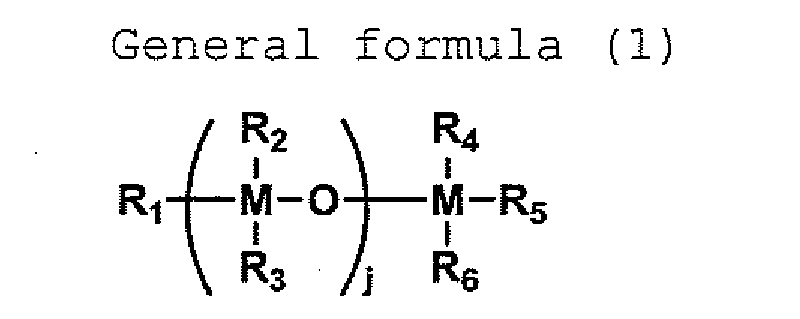
M represents Si, Ti, Ge, Zr, or Sn in general formula
(1). R1 - R6 represent a hydrogen atom or a monovalence group
respectively and at least one group among groups represented
by R1 - R6 is an organic group with fluorine atoms. The
organic groups which contain alkyl group, alkenyl group, or
alyl group which possess fluorine atoms should be used.
Trifluoromethyl group, perfluoroethyl group, perfluoropropyl
group, perfluorobutyl, 4, 4, 3, 3, 2, 2, 1, 1-octafluorobutyl
group as an alkyl group with fluorine atoms, for example, can
be provided. 3, 3, 3-trifluoro-1-propenyl group as an
alkenyl group with fluorine atoms, for example, can be
provided. Pentafluorophenyl group as an alyl group with
fluorine atoms, for example, can also be provided. Alkoxy
group, alkenyloxy group, and alyloxy group made from alkyl
group, alkenyl group, and alyl group with fluorine atoms
respectively can be employed.
An arbitrary number of fluorine atoms in an alkyl
group, an alkenyl group, and an alyl group may be bonded at
any bonding position of a carbon atom in a skeleton. But, at
least one or more fluorine atoms should be bonded. Carbon
atoms in skeletons of an alkyl group and an alkenyl group,
for example, may also be substituted by other atoms of
oxygen, nitrogen, sulfur and others and also by divalent
groups including oxygen, nitrogen, and sulfur, for example, a
calbonyl group, a thiocalbonyl group, and so forth.
A hydrogen atom or a monovalent group other than
organic groups with fluorine atoms can be represented in the
group shown by R1 - R6. Hydroxy group, amino group,
isocyanate group, halogen group, alkyl group, cycloalkyl
group, alkenyl group, alyl group, alkoxy group, alkenyloxy
group, alyloxy group, and so forth as a monovalent group, for
example, can be given. But, those are not limited. The
symbol j is represented by an integer which can be 0 to 150
and an integer of 0 to 50 is preferably used. An integer of
0 to 20 is especially preferable.
A chlorine atom, a bromine atom, and an iodine atom
in the aforementioned monovalent group are preferable as a
halogen atom. Alkoxy group, alkenyloxy group, and alyloxy
group among those groups such as alkyl group, alkenyl group,
alyl group, alkoxy group, alkenyloxy group, and alyloxy group
as the monovalent group, mentioned above, are preferably
used.
Si and Ti among metallic atoms, which are represented
by M, are preferably used.
The aforementioned monovalent group may be substituted
by other groups though they are not especially specified and
preferable substitution groups include amino group, hydroxyl
group, isocyanate group, halogen atoms such as fluorine atom,
chlorine atom, bromine atom and so forth, and groups such as
alkyl group, cycloalkyl group, alkenyl group, alyl group such
as phenyl group and so forth, alkoxy group, alkenyloxy group,
alyloxy group, acyl group, acyloxy group, alkoxycarbonyl
group, alkaneamido group, alylamido group, alkylcarbamoyl
group, alylcarbamoyl group, silyl group, alkylsilyl group,
alkoxysilyl group, and so forth.
The aforementioned organic group with fluorine atoms or
other groups represented by R1 - R6 may be of the structure
which contains a plurality of metallic atoms substituted by
the group which is represented by R1R2R3M-.
(M represents the aforementioned metallic atom. R1, R2, and
R3 represent a monovalent group respectively. The
aforementioned organic group with fluorine atoms or a group
other than the aforementioned organic group with fluorine
atoms which is represented by R1 - R6 is given as a
monovalent group.) Si and Ti as those metallic atoms are
given and for example, silyl group, alkylsilyl group,
alkoxysilyl group, and so forth can be given.
Groups with fluorine atoms represented by R1 - R6 which
are an alkyl group and an alkenyl group or an alkyl group and
an alkenyl group based on an Alkoxy group and an alkenyloxy
group which can be formed by those groups with fluorine atoms
are preferable to be shown in general formula (F).
General formula (F)
Rf-X-(CH2)k-
Rf in general formula (F) represents an alkyl group and an
alkenyl group in which at least one hydrogen atom is
substituted by fluorine atoms and for examples, those groups,
mentioned below, are preferable.
Perfluoroalkyl group and so forth such as trifluoromethyl group, pentafluoroethyl group, perfluorooctyl group, and heptafluoropropyl group, 3, 3, 3-trifluoropropyl group, and 4, 4, 3, 3, 2, 2, 1, 1-octafluorobutyl group and alkenyl group substituted by fluorine atoms such as 1, 1, 1-trifluoro-2-chlorpropenyl group and so forth.
Groups such as trifluoromethyl group, pentafluoroethyl group, perfluorooctyl group, heptafluoropropyl group and alkyl group possessing at least two or more fluorine atoms such as 3, 3, 3-trifluoropropyl group, 4, 4, 3, 3, 2, 2, 1, 1 octafluorobutyl group and so forth are especially preferable.
Rf-X-(CH2)k-
Perfluoroalkyl group and so forth such as trifluoromethyl group, pentafluoroethyl group, perfluorooctyl group, and heptafluoropropyl group, 3, 3, 3-trifluoropropyl group, and 4, 4, 3, 3, 2, 2, 1, 1-octafluorobutyl group and alkenyl group substituted by fluorine atoms such as 1, 1, 1-trifluoro-2-chlorpropenyl group and so forth.
Groups such as trifluoromethyl group, pentafluoroethyl group, perfluorooctyl group, heptafluoropropyl group and alkyl group possessing at least two or more fluorine atoms such as 3, 3, 3-trifluoropropyl group, 4, 4, 3, 3, 2, 2, 1, 1 octafluorobutyl group and so forth are especially preferable.
X is either a single bond or a divalent group. There
are -O-, -S-, groups such as -NR-(R represents a hydrogen
atom or an alkyl group.), and so forth and also groups of
-CO-, -CO-O-, -CONH-, -SO2NH-, -SO2-O-, and -OCONH-, and so
forth which represent divalent groups.

Symbol k is an integer of 0 to 50. But, an integer of
0 to 30 is preferably used.
Substitution groups other than fluorine atoms for Rf
may be substituted and groups which are similar to those
exemplified as substitution groups for the aforementioned R1
- R6 can be given. Skeleton carbon atoms in Rf may be
partially substituted by, for examples, groups of other atoms
such as -O-, -S-, -NR0- (R0 represents a hydrogen atom or an
alkyl group which is either substituted or not and may also
be a group expressed in general formula (F).), carbonyl
group, -NHCO-, -CO-O-, -SO2NH-, and so forth.
Compounds which are hereinafter expressed in general
formula (2) among those expressed by aforementioned general
formula (1) are preferable.
General formula (2)
[Rf-X-(CH2)k]q-M(R10)r(OR11)t
M in general formula (2) represents the same metallic atom
as in aforementioned general formula (1). Rf and X in
general formula (2) represent the same groups as expressed in
general formula (F) and the same integer represented by k is
also applied. R10 represents an alkyl group or an alkenyl
group and also R11 represents an alkyl group, an alkenyl
group, or an alyl group. Preferably those groups represent
an alkyl group and an alkenyl group which are not substituted
though they may be substituted by the same groups as those
provided as substitution groups of R1 - R6 in aforementioned
general formula (1), and
q + r + t = 4, q ≥ 1, and t ≥ 1 are also satisfied respectively. A linkage ring of R10 and R10
may be formed in the case of r ≥ 2.
[Rf-X-(CH2)k]q-M(R10)r(OR11)t
q + r + t = 4, q ≥ 1, and t ≥ 1 are also satisfied respectively. A linkage ring of R10 and R10
may be formed in the case of r ≥ 2.
Compounds which are expressed in general formula (3)
described later among those expressed in general formula (2)
are preferable.
General formula (3)
Rf-X-(CH2)k-M(ORr2)3
Rf, X, and k are used synonymously with those in
aforementioned general formula (2). R12 is also used
synonymously with R11 in general formula (2). M is also the
same M as appeared in general formula (2). Si and Ti as M
are preferably used. Especially Si is preferably used.
Rf-X-(CH2)k-M(ORr2)3
Compounds which are shown in general formula (4)
described later are given as another preferable example of
organometallic compounds possessing fluorine atoms in the
present invention.

Herein, M and R1 - R6 are used synonymously with R1 - R6
in aforementioned general formula (1). At least one of R1 -
R6 is an organic group with fluorine atoms and a group
expressed by aforementioned general formula (F) is
preferable. R7 represents a hydrogen atom or an alkyl group
which is either substituted or not. The symbol j represents
an integer which can be 0 to 100 and an integer of 0 to 50 is
preferably used. An integer of 0 to 20 is especially
preferable.
Organometallic compounds containing fluorine atoms
which are expressed in general formula (5) described later
are given as other preferable compounds containing fluorine
atoms which are employed in the present invention.
General formula (5)
[Rf-X-(CH2)k-Y]m-M(R8)n(OR9)p
M represents In, Al, Sb, Y or La in general formula (5). Rf
and X represent the same groups of Rf and X as appeared in
aforementioned general formula (F) and Y is
either a single bond or an oxygen atom. The symbol k is
similarly an integer of 0 to 50 and an integer not more than
30 is preferable. R9 represents an alkyl group or an alkenyl
group and also R8 represents an alkyl group, an alkenyl
group, or an alyl group. They may be substituted by the same
groups as those provided as substitution groups of R1 - R6 in
aforementioned general formula (1). In general formula (5),
the following conditions are shown. m + n + p = 3 holds, and
m is at least 1, n represents integers of 0 - 2 and p also
represents integers of 0 - 2. The condition of m + p = 3,
namely of n = 0 is preferable.
[Rf-X-(CH2)k-Y]m-M(R8)n(OR9)p
Organometallic compounds containing fluorine atoms
which are expressed in general formula (6) described later
are provided as other preferable compounds containing
fluorine atoms which are employed in the present invention.
General formula (6)
Rf1(OC3F6)ml-O-(CF2)nl-(CH2)pl-Z-(CH2)ql-Si-(R2)3
Rf1(OC3F6)ml-O-(CF2)nl-(CH2)pl-Z-(CH2)ql-Si-(R2)3
As for general formula (6), Rf1 represents a straight
chain or a branched chain perfluoroalkyl group having a
carbon number between 1 and 16, R2 represents a hydrolysis
group, and Z represents either -OCONH- or -O-. The symbol ml
represents an integer between 1 and 50, nl represents an
integer between 0 and 3, p1 represents an integer between 0
and 3, ql represents an integer between 1 and 6, and 6 ≥ nl +
pl > 0 holds.
A carbon number of a straight chain or a branched chain
perfluoroalkyl group which can be introduced into Rf1 should
be 1 - 16. The number 1 - 3 is especially preferable.
Accordingly, -CF3, -C2F5, -C3F7, and so forth as Rf1 are
preferably used.
-Cl, -Br, -I, -OR11, -OCOR11, -CO(R11)C=C(R12)2,
-ON=C(R11)2, -ON=CR13, -N(R12)2, -R12NOCR11, and so forth as
hydrolysis groups which can be introduced to R2 are
preferably used. R11 represents an aliphatic hydrocarbon
group having a carbon number between 1 and 10 such as an
alkyl group and so forth or an aromatic hydrocarbon group
having a carbon number between 6 and 20 such as a phenyl
group and so forth, R12 represents an aliphatic hydrocarbon
group having a carbon number between 1 and 5 such as a
hydrogen atom or an alkyl group and so forth, and R13
represents a divalent aliphatic hydrocarbon group having a
carbon number between 3 and 6 such as an alkylidene group and
so forth. -OCH3, -OC2H5, -OC3H7, -OCOCH3, and -NH2 among those
hydrolysis groups are preferably used.
The suffix ml is preferably 1 - 30, and more preferably
5 - 20. The suffix nl is more preferably either 1 or 2, pl
is also more preferably either 1 or 2, and ql is also more
preferably 1 - 3.
Organometallic compounds containing fluorine atoms
which are expressed in general formula (7) described later
are given as other preferable compounds containing fluorine
atoms which are employed in the present invention.
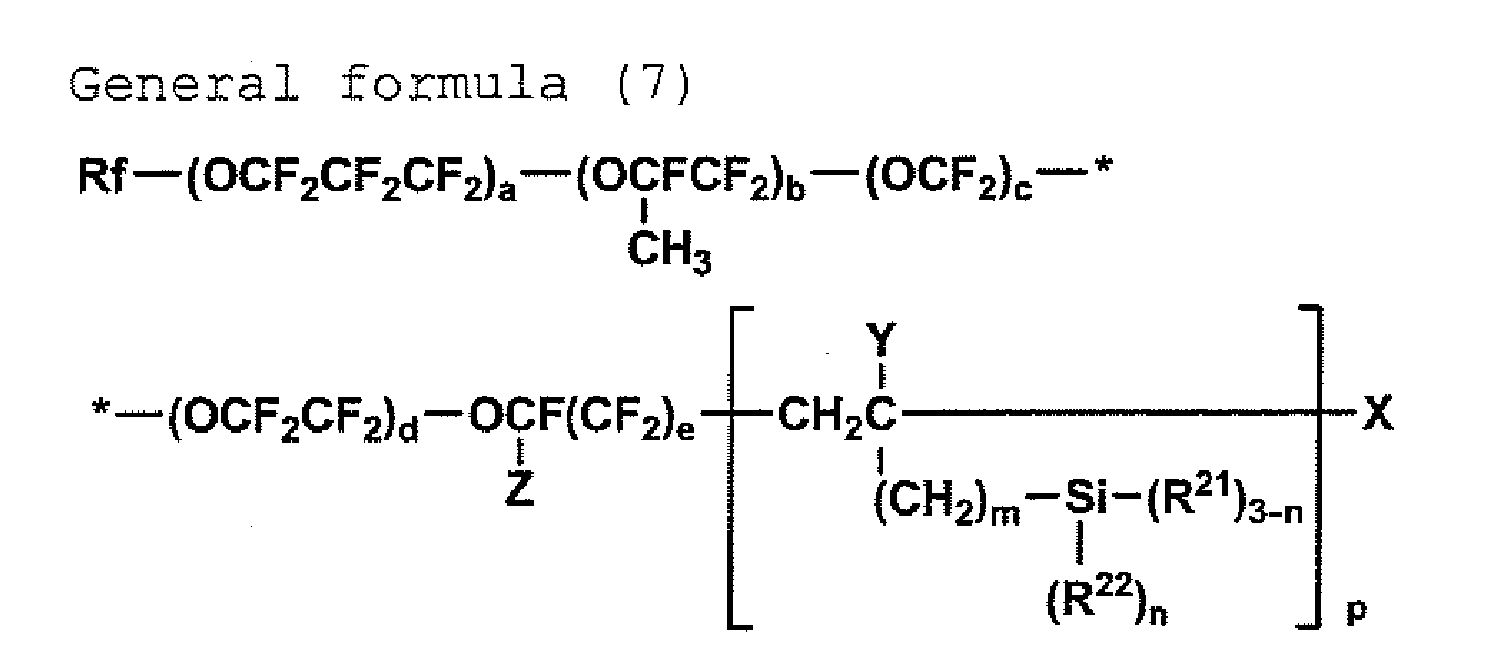
In general formula (7), Rf represents a straight chain
or a branched chain perfluoroalkyl group having a carbon
number between 1 and 16, X represents an iodine atom or a
hydrogen atom, Y represents a hydrogen atom or a lower
Alkyl group, Z represents a fluorine atom or a
trifluoromethyl group, R21 represents a hydrolyzable group,
and R22 represents a hydrogen atom or an inert and monovalent
organic group. Suffixes a, b, c, and d are integers between
0 and 200 respectively, e is either 0 or 1, m and n are
respectively integers between 0 and 2, and p is an integer
between 1 and 10.
In aforementioned general formula (7), usually Rf
represents a straight chain or a branched chain
perfluoroalkyl group having a carbon number between 1 and 16.
And those groups such as a CF3 group, a C2F5 group, and a C3F7
group are preferable. A lower alkyl group possessing a
carbon number between 1 and 5, represented by Y, can be
given.
Halogen atoms such as a chlorine atom, a bromine atom,
and an iodine atom, a R23O group, a R23COO group, a
(R24) 2C=C (R23) CO group, a (R23)2C=NO group, a R25C=NO group, a
(R24) 2N group, and a R23CONR24 group as hydrolyzable groups
represented by R21 should be used, where R23 represents an
aliphatic hydrocarbon group having a carbon number usually
between 1 and 10 such as an alkyl group and so forth or
an aromatic hydrocarbon group having a carbon number usually
between 6 and 20 such as a phenyl group and so forth, R24
represents a lower aliphatic hydrocarbon group having a
carbon number usually between 1 and 5 such as a hydrogen
atom, an alkyl group and so forth, and R25 represents a
divalent aliphatic hydrocarbon group having a carbon number
usually between 3 and 6 such as an alkylidene group and so
forth.
A chlorine atom, a CH3O group, a C2H5O group, and a
C3H7O group among those hydrolysis groups are preferably
used.
R22 represents a hydrogen atom or an inert, monovalent
organic group and represents a monovalent hydrocarbon group
having a carbon number usually between 1 and 4 such as an
alkyl group and so forth preferably. Suffixes a, b, c, and d
are integers between 0 and 200 respectively and those
integers between 1 and 50 are preferable. m and n are
integers between 0 and 2 and they should be 0 preferably.
The symbol p represents integers of 1 or not less than 2, an
integer between 1 and 10 is preferable, and an integer
between 1 and 5 is especially preferable. The number-average
molecular weight is 5 x 10² - 1 x 10⁵ and it is 1 x 10³ - 1 x
104 preferably.
A compound with a preferable structure as a silane
compound expressed in aforementioned general formula (7) is
one where Rf is a C3F7 group, a is an integer between 1 and
50, b, c, and d are 0 respectively, e is 1, Z is a fluorine
atom, and n is 0.
Organometallic compounds having organic groups with
fluorine atoms used preferably as a silane compound
containing fluorine atoms and typical compounds among those
compounds expessed in aforementioned general formulae (1) -
(7) in the present invention are given below. But, the
invention is not limited only to those compounds.
- 83 : (perfluoropropyloxy)dimethylsilane
- 84 : tris(perfluoropropyloxy)methylsilane
- 85 : dimethylbis(nonafluorobutoxy)silane
- 86 : methyltris(nonafluorobutoxy)silane
- 87 : bis(perfluoropropyloxy)diphenylsilane
- 88 : bis(pexfluoroprapyloxy)methylvinylsilane
- 89 : bis(1, 1, 1, 3, 3, 4, 4, 4-octafluorobutoxy) dimethylsilane
- 90 : bis(1, 1, 1, 3, 3, 3-hexafluoroisopropoxy) dimethylsilane
- 91 : tris(1, 1, 1, 3, 3, 3- hexafluoroisopropoxy) methylsilane
- 92 : tetrakis(1,1,1,3,3,3-hexafluaroisoproppxy)silane
- 93 : dimethylbis(nonafluoro-t-butoxy)silane
- 94 : bis(1, 1, 1, 3, 3, 3-hexafluoroisopropoxy) diphenylsilane
- 95 : tetrakis(1, 1, 3, 3-tetrafluoroisopropoxy)silane
- 96 : bis [1, 1-bis(trifluoromethyl)ethoxy]dimethylsilane
- 97 : bis(1, 1, 1, 3, 3, 4, 4, 4-octafluoro-2-butoxy) dimethylsilane
- 98 : methyltris[2, 2, 3, 3, 3-pentafluoro-1,1-bis (trifluoromethyl)propoxy]silane
- 99 : diphenylbis[2, 2, 2-trifluoro-1-(trifluoromethyl)-1-tolylethoxy]silane
- 100 : (CF3CH2Si (CH2-NH2)
- 101 : (CF3CH2)3Si-N(CH3)2

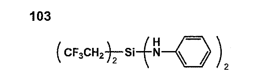
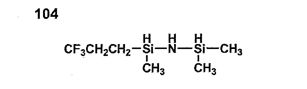

- 106 : CF3CH2-CH2TiCl3
- 107 : CF3(CF2)3CH2CH2TiCl3
- 108 : CF3(CF2)5CH2Ti(OCH3)3
- 109 : CF3(CF2)7CH2CH2TiCl3
- 110 : Ti(OC3F7)4
- 111 : (CF3CH2-CH2O)3TiCl3
- 112 : (CF3C2H4) (CH3)2Ti-O-Ti (CH3)3
- 113 : CF3(CF2)3(CH2CH2O(CH2)3GeCl
- 114 : CF3(CF2)3CH2CH2OCH2Ge(OCH3)3
- 115 : (C3F7O)2Ge(OCH3)2
- 116 : [(CF3)2CHO]4Ge
- 117 : [(CF3)2CHO]4Zr
- 118 : (C3F7CH2CH2)2Sn(OC2H5)2
- 119 : (C3F7CH2CH2) Sn (OC2H5)3
- 120 : Sn(OC3F7)4
- 121 : CF3CH2CH2CH2In (OCH3)2
- 122 : In(OCH2CH2OC3F7)3
- 123 : Al(OCH2CH2OC3F7)3
- 124 : Al(OC3F7)3
- 125 : Sb(OC3F7)3
- 126 : Fe(OC3F7)3
- 127 : Cu(OCH2CH2OC3F7)2
- 128 : C3F7(OC3F6)24O(CF2)2CH2OCH2Si(OCH3)3

Each compound given by those actual examples has been
put on the market by Dow Corning Toray Silicone Co.,Ltd,
Shin-Etsu Chemical Co.,Ltd, Daikin Industries,Ltd (OPTOOL
DSX, for example), and Gelest Inc., Solvey Solexis Co., Ltd.,
and so forth and those compounds can be easily purchased.
Those compounds can be manufactured by the synthesis method
described in J.Fluorine Chem., 79(1),87(1996), Zairyou
Gijutsu,16(5),209(1998), Collect. Czech. Chem.
Commun.,vol.44,750-755, J. Amer. Chem. Soc. vol.112,2341-2348(1990),
Inorg. Chem.,vol.10,889-892(1971), USP
No.3,668,233, Japanese Patent O.P.I. Publication No.58-122979,
Japanese Patent O.P.I. Publication No.7-242675,
Japanese Patent O.P.I. Publication No.9-61605, Japanese
Patent O.P.I. Publication No.11-29585, Japanese Patent O.P.I.
Publication No.2000-64348, Japanese Patent O.P.I. Publication
No.2000-144097, and so forth, for examples. Or, those
compounds can be manufactured by synthesis techniques based
on this method.
Examples provided for the preferable organosilicon
compound include types of tri alkoxy silanes, tri acyloxy
silane and tri phenoxy silanes such as methyl trimethoxy
silane, methyl triethoxy silane, methyl trimethoxyethoxy
silane, methyl triacetoxy silane, methyl tripropxy silane,
methyl tributoxy silane, ethyl trimethoxy silane, ethyl
triethoxy silane, vinyl trimethoxy silane, vinyl triethoxy
silane, vinyl triacetoxy silane, vinyl trimethoxyethoxy
silane, phenyl trimethoxy silane, phenyl triethoxy silane,
phenyl triacetoxy silane, γ-chloropropyl trimethoxy silane,
γ-chloropropyl triethoxy silane, γ-chloropropyl triacetoxy
silane, γ-methacryloxypropyl trimethoxy silane, γ-aminopropyl
trimethoxy silane, γ-aminopropyl triethoxy silane,
γ-mercaptopropyl trimethoxy silane, γ-mercaptopropyl
triethoxy silane, N-β-(aminoethyl)-γ-aminopropyl trimethoxy
silane, β-cyanoethyl triethoxy silane, methyl triphenoxy
silane, chloromethyl trimethoxy silane, chloromethyl
triethoxy silane, glycidoxymethyl trimethoxy silane,
glycidoxymethyl triethoxy silane, α-glycidoxyethyl
trimethoxy silane, α-glycidaxyethyl triethoxy silane,
β-glycidoxyethyl trimethoxy silane, β-glycidoxyethyl
triethoxy silane, α-glycidoxypropyl trimethoxy silane,
α-glycidoxypropyl triethoxy silane, β-glycidoxypropyl
trimethoxy silane, β-glycidoxypropyl triethoxy silane,
γ-glycidoxypropyl trimethoxy silane, γ-glycidoxypropyl
triethoxy silane, γ-glycidoxypropyl tripropoxy silane,
γ-glycidoxypropyl tributoxy silane, γ-glycidoxypropyl
trimethoxyethoxy silane, γ-glycidoxypropyl triphenoxy silane,
α-glycidoxybutyl trimethoxy silane, α-glycidoxybutyl
triethoxy silane, β-glycidoxybutyl trimethoxy silane,
β-glycidoxybutyl triethoxy silane, γ-glycidoxybutyl
trimethoxy silane, γ-glycidoxybutyl triethoxy silane,
δ-glycidoxybutyl trimethoxy silane, δ-glycidoxybutyl
triethoxy silane, (3, 4-epoxycyclohexyl) methyl trimethoxy
silane, (3, 4-epoxycyclohexyl) methyl triethoxy silane,
β-(3, 4-epoxycyclohexyl) ethyl trimethoxy silane,
β-(3, 4-epoxycyclohexyl) ethyl triethoxy silane,
β-(3, 4-epoxycyclohexyl) ethyl tripropoxy silane,
β-(3, 4-epoxycyclohexyl) ethyl tributoxy silane,
β-(3, 4-epoxycyclohexyl) ethyl trimethoxyethoxy silane,
γ-(3, 4-epoxycyclohexyl) propyl trimethoxy silane,
β-(3, 4-epoxycyclohexyl) ethyl triphenoxy silane,
γ-(3, 4-epoxycyclohexyl) propyl trimethoxy silane,
γ-(3, 4-epoxycyclohexyl) propyl triethoxy silane, and
δ-(3, 4-epoxycyclohexyl) butyl trimethoxy silane; and types
of dialkoxy silane, diphenoxy silane, diacyl oxysilane,
trimethyl ethoxy silane, trimethyl methoxy silane,
3, 3, 3-trifluoropropyltrimethoxysilane,
dimethoxymethyl-3, 3, 3-trifluoropropylsilane,
fluoroalkylsilane, hexamethyldisilane, and
hexamethyldisiloxane such as dimethyl dimethoxy silane,
phenylmethyl dimethoxy silane, dimethyl diethoxy silane,
phenylmethyl diethoxy silane,
γ-chloropropylmethyl dimethoxy silane, γ-chloropropylmethyl
diethox silane, dimethyl diacetoxy silane,
γ-methacryloxypropylmethyl dimethoxy silane,
γ-methacryloxypropylmethyl diethoxy silane,
γ-mercaptopropylmethyl dimethoxy silane,
γ-mercaptopropylmethyl diethoxy silane, γ-aminopropylmethyl
dimethoxy silane, γ-aminopropylmethyl diethoxy silane,
methylvinyl dimethoxy silane, methylvinyl diethox silane,
glycidoxymethylmethyl dimethoxy silane, glycidoxymethylmethyl
diethoxy silane, α-glycidoxyethylmethyl dimethoxy silane,
α-glycidoxyethylmethyl diethoxy silane,
β-glycidoxyethylmethyl dimethoxy silane,
β-glycidoxyethylmethyl diethoxy silane,
α-glycidoxypropylmethyl dimethoxy silane,
α-glycidoxypropylmethyl diethoxy silane,
β-glycidoxypropylmethyl dimethoxy silane,
β-glycidoxypropylmethyl diethoxy silane,
γ-glycidoxypropylmethyl dimethoxy silane,
γ-glycidoxypropylmethyl diethoxy silane, γ-glycidoxypropyl
methyl dipropoxy silane, γ-glycidoxypropylmethyl
dibutoxyethoxy silane, γ-glycidoxypropylmethyl
dimethoxyethoxy silane,
γ-glycidoxypropylmethyl diphenoxy silane, γ-glycidoxypropyl
methyl diacetoxy silane, γ-glycidoxypropylethyl dimethoxy
silane, γ-glycidoxypropylethyl diethoxy silane,
γ-glycidoxypropylvinyl dimethoxy silane,
γ-glycidoxypropylvinyl diethoxy silane,
γ-glycidoxypropylphenyl dimethoxy silane and
γ-glycidoxypropylphenyl diethoxy silane.
Organosilicon compounds are not limited to the above
compounds. They may also be employed singly, or not less
than two different kinds of compounds may be used at the same
time.
Among the foregoing compounds, preferably provided are
methyl triethoxy silane, ethyl triethoxy silane, dimethyl
diethoxy silane, dimethyl dimethoxy silane, isopropyl
trimethoxy silane, isopropyl triethoxy silane, butyl
trimethoxy silane and trimethyl ethoxy silane.
Compounds expressed by following general formula (8)
are used as the other organosilicon compound, wherein n is 0
- 2000. R81 - R88 are hydrogen atoms, or straight, branched or
cyclic hydrocarbon groups which may be either saturated or
unsaturated. Each of them may be either the same or
different.

Compounds fitted into general formula (1) can be
selected from Silicon compound reagents produced by Shinetsu
chemicals Co., Ltd., or reagents described in the compound
catalogs of Metal-organics for material & polyer technology
(Gelest, Inc.) and Silicon chemicals (Chisso corporation) to
be utilized, and examples of those compounds capable of using
are described below. Of course, they are not limited to
those compounds.

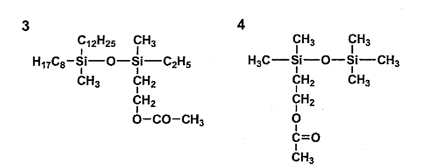
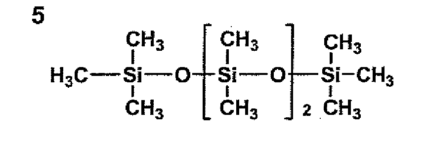
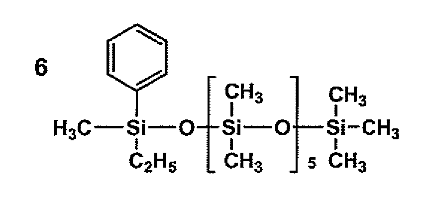
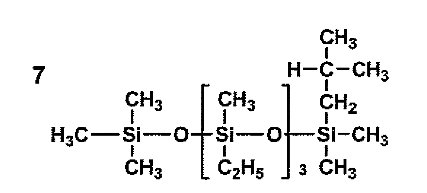
Fluorinated compounds can be used as the other raw
material, and organic fluorinated compounds such as
fluorinated carbon gas, fluorinated hydrocarbon gas and
others can be used. Examples of the fluorinated carbon gas
include tetrafluoromethane, tetrafluoroethylene,
hexafluoropropylene and octafluorocyclobutane. Examples of
the above fluorinated hydrocarbon gas include
difluoromethane, tetrafluoroethane, tetrafluoropropylene and
trifluoropropylene. Examples provided, further, include
halide of a fluorinated hydrocarbon compound such as
chlorotrifluoromethane, chlorodifluoromethane or
dichlorotetrafluorocyclobuthane, fluoroalcohol such as
trifluoromethanol or pentafluoroethanol, fluorinated
aliphatic acid such as trifluoroacetic acid or
pentafluoropropione acid, and an organic fluorinated compound
such as fluorinated ketone of hexafluoroacetone and so forth.
They are not limited to those compounds and acids described
above. Those compounds may contain a fluorinated
ethlenically unsaturated group within a molecule.
It is preferable that a film of the present invention
is formed on a gate insulating layer, and an organic
semiconductor layer is provided further on the film. The
film thickness is preferably from a thickness of a single
molecular layer to 100 nm, and more preferably from a
thickness of a single molecular layer to 10 nm.
A contact angle against pure water of a surface of the
film is also required to be not less than 50° to acquire
effect of the present invention, preferably 70 - 170°, and
more preferably 90 - 130°. An ON/OFF ratio and carrier
mobility of a transistor decrease prominently when the
contact angle is low, and coatability of a semiconducting
material solution also drops when the contact angle is too
high.
Though a bottom gate type thin-film transistor depends
largely on surface profiles of the substrate, the gate
electrode and the gate insulating layer, it is preferable
from the aspect of carrier mobility that surface roughness Ra
of the film surface is roughly 0.01 - 10 nm.
Even though as a film formation method there are
methods provided other than the foregoing atmospheric
pressure plasma method such as a thermal CVD method in which
a film is formed via thermal reaction by supplying reactive
gas containing the raw material onto a heated substrate in
the range of 50 - 500 °C, and a common plasma CVD in which a
film is formed under reduced pressure of 0.01 - 100 Pa
employing the foregoing apparatus, and both discharge gas and
reactive gas, to acquire effect of the present invention, the
atmospheric pressure plasma method is most preferably used
from the aspect of increased mobility, film evenness, speed
of forming a film, and efficient productivity.
After pretreatment (washing) is conducted by exposing a
substrate for the film formation in the present invention,
placed in discharge space, to excited discharge gas, it is
preferred that the film formation is carried out. 90 - 99.9%
by volume of the foregoing inert gas and 0.01 - 10% by volume
of at least one kind selected from oxygen, ozone, hydrogen
peroxide, and hydrogen are used as the mixed gas at this
time.
Ether nitrogen or argon, and oxygen are preferably
used. Effect of removing impurities which affect adversely
to transistor characteristics can be obtained by the above
treatment. Further, effect of enhanced reactivity via
reactive gas to form a film of the present invention as well
as effect of improved evenness and density of the film, and
increased carrier mobility of a transistor can be obtained,
when there are provided metallic oxides such as silicon oxide
and so forth on the surface of a substrate.
It is desired that a contact angle against pure water
of a surface of the film is set to 1 - 30°, when there are
provided metallic oxides such as silicon oxide and so forth
on the surface of a substrate, and preferably to 3 - 20°.
The common information concerning an organic thin-film
transistor and its manufacturing method in the present
invention will subsequently be described.
As the organic thin-film transistor, there are a top
gate type transistor (Fig. 12(a) and Fig. 12(b)) possessing
organic semiconductor layer 5 on substrate F, the organic
semiconductor layer contacting source electrode 6 and drain
electrode 7 on the surface of the support, gate insulating
layer 3 on the organic semiconductor layer, and a gate
electrode on the gate insulating layer, and a bottom gate
type transistor (Fig. 12(c))possessing gate electrode 2 on
the surface of substrate F, organic semiconductor layer 5 on
the substrate, the organic semiconductor layer contacting
source electrode 6 and drain electrode 7, the gate insulating
layer on the organic semiconductor layer, and the gate
electrode on the gate insulating layer. Each of the above
types is acceptable. The bottom gate type, however, is
specifically preferable in the case of the present invention.
The organic thin-film transistor of the present
invention possesses either a subbing layer containing a
compound selected from inorganic oxides or inorganic
nitrides, or a subbing layer containing a polymer.
Examples of the inorganic oxide contained in the
subbing layer include silicon oxide, aluminum oxide, tantalum
oxide, titanium oxide, tin oxide, vanadium oxide, barium
strontium titanate, barium zirconate titanate, zirconic acid
lead carbonate, lead lanthanum titanate, strontium titanate,
barium titanate, barium magnesium fluoride, bismuth titanate,
strontium bismuth titanate, strontium bismuth tantalate,
bismuth niobate tantalate, and yttrium trioxide. An
inorganic nitride such as silicon nitride or aluminum nitride
can be also suitably used.
Of these, silicon oxide, aluminum oxide, tantalum
oxide, titanium oxide, or silicon nitride is preferred.
In the present invention, the subbing layer containing
a compound selected from inorganic oxides or inorganic
nitrides is preferably formed according to the atmospheric
pressure plasma method described above.
Examples of the polymer used in the subbing layer
include a polyester resin, a polycarbonate resin, a cellulose
resin, an acryl resin, a polyurethane resin, a polyethylene
resin, a polypropylene resin, a polystyrene resin, a phenoxy
resin, a norbornene resin, an epoxy resin, vinyl chloride-vinyl
acetate copolymer, a vinyl chloride resin, vinyl
acetate-vinyl alcohol copolymer, a partially saponificated
vinyl chloride-vinyl acetate copolymer, vinyl chloride-vinylidene
chloride copolymer, vinyl chloride-acrylonitrile
copolymer, ethylene-vinyl alcohol copolymer, polyvinyl
alcohol, chlorinated polyvinyl chloride, ethylene-vinyl
chloride copolymer, ethylene-vinyl acetate copolymer, a
polyamide resin, an ethylene-butadiene resin, a butadiene-acrylonitrile
resin, a silicone resin, and a fluorine-containing
resin.
As the organic semiconductive materials in the present
invention, π-conjugated materials are used. Examples of the
π-conjugated materials include polypyrroles such as
polypyrrole, poly(N-substituted pyrrole), poly(3-substituted
pyrrole), and poly(3,4-disubstituted pyrrole); polythiophenes
such as polythiophene, poly(3-substituted thiophene),
poly(3,4-disubstituted thiophene), and polybenzothiophene;
polyisothianaphthenes such as polyisothianaphthene;
polythienylenevinylenes such as polythienylenevinylene;
poly(p-phenylenevinylenes) such as poly(p-phenylenevinylene);
polyanilines such as polyaniline, poly(N-substituted
aniline), poly(3-substituted aniline), and poly(2,3-substituted
aniline); polyacetylnenes such as polyacetylene;
polydiacetylens such as polydiacetylene; polyazulenes such as
polyazulene; polypyrenes such as polypyrene; polycarbazoles
such as polycarbazole and poly(N-substituted carbazole),
polyselenophenes such as polyselenophene; polyfurans such as
polyfuran and polybenzofuran; poly(p-phenylenes) such as
poly(p-phenylene); polyindoles such as polyindole;
polypyridazines such as polypyridazine; polyacenes such as
naphthacene, pentacene, hexacene, heptacene,
dibenzopentacene, tertabenzopentacene, pyrene, dibenzopyrene,
chrysene, perylene, coronene, terylene, ovalene, quoterylene,
and circumanthracene; derivatives (such as triphenodioxazine,
triphenodithiazine, hexacene-6,15-quinone) in which some of
carbon atoms of polyacenes are substituted with atoms such as
N, S, and O or with a functional group such as a carbonyl
group; polymers such as polyvinyl carbazoles, polyphenylene
sulfide, and polyvinylene sulfide; and polycyclic
condensation products described in Japanese Patent O.P.I.
Publication No. 11-195790.
Further, oligomers having repeating units in the same
manner as in the above polymers, for example, thiophene
hexamers including α-sexithiophene, α, ω-dihexyl-α-sexithiophene,
α,ω-dihexyl-α-quiinquethiophene, and α,ω-bis(3-butoxypropyl)-α-sexithiophene,
or styrylbenzene
derivatives, can be suitably employed.
Further, listed are metallophthalocyanines such as
copper phthalocyanine, and fluorine-substituted copper
phthalocyanines described in Japanese Patent O.P.I.
Publication No. 11-251601; tetracarboxylic acid diimides of
condensed ring compounds including naphthalene
tetracarboxylic acid imides such as naphthalene 1,4,5,8-teracarboxylic
acid diimide, N,N'-bis(4-trifluoromethylbenzyl) naphthalene
1,4,5,8-tretracarboxylic
acid diimide, N,N'-bis(1H,1H-perfluoroctyl) naphthalene
1,4,5,8-tetracarboxylic acid diimide derivatives, N,N'-bis(1H,1H-perfluorobutyl) naphthalene
1,4,5,8-tetracarboxylic
acid diimide derivatives, N,N'- dioctylnaphthalene 1,4,5,8-tetracarboxylic
acid diimide derivatives, and naphthalene
2,3,6,7-tetracarboxylic acid diimides, and anthracene
tetracarbocylic acid diimides such as anthracene 2,3,6,7-tetracarboxylic
acid diimides; fullerenes such as C60, C70,
C76, C78, and C84; carbon nanotubes such as SWNT; and dyes such
as merocyanines and hemicyanines.
Of these π conjugated compounds, preferably employed is
at least one selected from the group consisting of oligomers
which have thiophene, vinylene, thienylenevinylene,
phenylenevinylene, p-phenylene, their substitution product or
at least two kinds thereof as a repeating unit and have a
repeating unit number n of from 4 to 10, polymers which have
the same unit as above and a repeating unit number n of at
least 20, condensed polycyclic aromatic compounds such as
pentacene, fullerenes, condensed cyclic tetracarboxylic acid
diimides of condensed ring compounds, and metallic
phthalocyanines.
Further, employed as other materials for organic
semiconductors may be organic molecular complexes such as a
tetrathiafulvalene (TTF)-tetracyanoquinodimethane (TCNQ)
complex, a bisethylenetetrathiafulvalene (BEDTTTF)-perchloric
acid complex, a BEDTTTF-iodine complex, and a TCNQ-iodine
complex. Still further, employed may be σ conjugated
polymers such as polysilane and polygermane, as well as
organic-inorganic composite materials described in Japanese
Patent O.P.I. Publication No. 2000-260999.
In the present invention, the organic semiconductor
layer may be subjected to a so-called doping treatment by
incorporating in the layer, materials working as an acceptor
which accepts electrons, for example, acrylic acid,
acetamide, materials having a functional group such as a
dimethylamino group, a cyano group, a carboxyl group and a
nitro group, benzoquinone derivatives, or tetracyanoethylene,
tetracyanoquinodimethane or their derivatives, or materials
working as a donor which donates electrons, for example,
materials having a functional group such as an amino group, a
triphenyl group, an alkyl group, a hydroxyl group, an alkoxy
group, and a phenyl group; substituted amines such as
phenylenediamine; anthracene, benzoanthracene, substituted
benzoanthracenes, pyrene, substituted pyrene, carbazole and
its derivatives, and tetrathiafulvalene and its derivatives.
The doping herein means that an electron accepting
molecule (acceptor) or an electron donating molecule (donor)
is incorporated in the organic semiconductor layer as a
dopant. Accordingly, the layer, which has been subjected to
doping, is one which comprises the condensed polycyclic
aromatic compounds and the dopant. As the dopant in the
present invention, a known dopant can be used.
The methods for forming the organic semiconductor layer
include a vacuum deposition method, a molecular beam
epitaxial growth method, an ion cluster beam method, a low
energy ion beam method, an ion plating method, a CVD method,
a sputtering method, a plasma polymerization method, an
electrolytic polymerization method, a chemical polymerization
method, a spray coating method, a spin coating method, a
blade coating method, a dip coating method, a casting method,
a roll coating method, a bar coating method, a die coating
method, and an LB method. These methods may be used
according to kinds of materials used. Of these, a spin
coating method, a blade coating method, a dip coating method,
a roll coating method, a bar coating method and a die coating
method by which a layer can be formed not only simply but
also precisely, using an organic semiconductor solution, are
preferably used in consideration of productivity. Herein,
toluene, xylene, chlorobenzene, chloroform, dichloromethane,
dichloroethane, or tetrahydrofuran (THF) can be employed as
an organic solvent used for the semiconducting material
solution.
When a precursor such as pentacene is soluble in a
solvent as disclosed in Advanced Material 1999, Vol. 6, p.
480-483, a precursor layer formed by coating of the precursor
solution may be heat treated to form an intended organic
material layer.
The thickness of the organic semiconductor layer is not
specifically limited. The thickness of an active layer
composed of the organic semiconductor materials often has a
great influence on properties of the resultant transistor.
Accordingly, the thickness of the layer differs due to kinds
of the organic semiconductor materials used, but it is
ordinarily not more than 1 µm, and preferably 10 - 300 nm.
In the present invention, materials for forming a
source electrode, a drain electrode and a gate electrode are
not specifically limited, as long as they are electrically
conductive. Examples thereof include platinum, gold, silver,
nickel, chromium, copper, iron, tin, antimony, lead,
tantalum, indium, palladium, tellurium, rhenium, iridium,
aluminum, ruthenium, germanium, molybdenum, tungsten, tin
oxide-antimony, indium oxide-tin (ITO), fluorine-doped zinc
oxide, zinc, carbon, graphite, glassy carbon, silver paste as
well as carbon paste, lithium, beryllium, sodium, magnesium,
potassium, calcium, scandium, titanium, manganese, zirconium,
gallium, niobium, sodium, sodium-potassium alloy, magnesium,
lithium, aluminum, magnesium/copper mixtures,
magnesium/silver mixtures, magnesium/aluminum mixtures,
magnesium/indium mixtures, aluminum/aluminum oxide mixtures,
and lithium/aluminum mixtures. Platinum, gold, silver,
copper, aluminum, indium, indium oxide-tin (ITO) and carbon
are preferred. Further, known electrically conductive
polymers whose electrical conductivity is improved by doping
are preferably used. Examples thereof include electrically
conductive polyaniline, electrically conductive polypyrrole,
electrically conductive polythiophene, and complex of
electrically conductive polyethylenedioxythiophene and
polystyrene sulfonic acid. Of these, ones, which provide a
low electric resistance at an interface with the
semiconductor layer, are preferred.
As a method for forming the electrode, there are a
method in which the electrode is formed according to a
commonly known photolithography or lift-off method from an
electrically conductive layer of the conductive material
described above formed according to a vacuum deposition
method or a sputtering method, a method in which the
electrode is formed according to thermal transfer of the
conductive material to a foil of a metal such as aluminum or
copper, and a method in which the electrode is formed by
etching a resist of the conductive material formed by an ink
jet method. The electrode may be formed by ejecting in the
form of electrode a solution or dispersion liquid of an
electrically conductive polymer or a dispersion liquid of
electrically conductive particles onto the surface on which
the electrode is to be directly formed by the ink jet method
or by subjecting to photolithography or laser ablation via
the coated layer of the solution or the dispersion liquid.
Further, employing ink or conductive paste containing an
electrically conductive polymer or electrically conductive
particles, the electrode may be formed by printing in the
electrode pattern onto the surface on which the electrode is
to be formed according to a printing method such as
letterpress printing, intaglio printing, planographic
printing or screen printing.
Various insulating films may be employed as the gate
insulating layer. The insulating layer is preferably an
inorganic oxide film composed of an inorganic oxide with high
dielectric constant. Examples of the inorganic oxide include
silicon oxide, aluminum oxide, tantalum oxide, titanium
oxide, tin oxide, vanadium oxide, barium strontium titanate,
barium zirconate titanate, zirconic acid lead carbonate, lead
lanthanum titanate, strontium titanate, barium titanate,
barium magnesium fluoride, bismuth titanate, strontium
bismuth titanate, strontium bismuth tantalate, bismuth
niobate tantalate, and yttrium trioxide. Of these, silicon
oxide, silicon nitride, aluminum oxide, tantalum oxide or
titanium oxide is particularly preferred. An inorganic
nitride such as silicon nitride or aluminum nitride can be
also suitably used.
The methods for forming the above film include a dry
process such as a vacuum deposition method, a molecular beam
epitaxial growth method, an ion cluster beam method, a low
energy ion beam method, an ion plating method, a CVD method,
a sputtering method, or an atmospheric pressure plasma
method, a wet process such as a spray coating method, a spin
coating method, a blade coating method, a dip coating method,
a casting method, a roll coating method, a bar coating
method, or a die coating method, and a patterning method such
as a printing method or an ink-jet method. These methods can
be used, depending on kinds of materials used in the
insulating layer.
As the typical wet process, there can be used a method
of coating a dispersion liquid obtained by dispersing
inorganic oxide particles in an organic solvent or water
optionally in the presence of a dispersant such as a
surfactant and drying, or a so-called sol gel method of
coating a solution of an oxide precursor such as an alkoxide
and drying.
Among the above, the preferred is an atmospheric
pressure plasma method. The formation of a gate insulating
layer is made possible at atmospheric pressure or
approximately atmospheric pressure by the foregoing apparatus
and the layer formation method.
In order to obtain a silicon oxide layer, inert gas
such as argon, helium, or nitrogen is provided as the
discharge gas, and a mixed gas of oxygen and a compound such
as tetraethoxy silane, tetramethoxy silane, or
tetraisopropoxy silane is also employed as the reactive gas.
A titanium oxide layer can also be acquired by changing these
silane compounds into a titanium compound such as tetraethoxy
titanium or tetraisopropoxy titanium. Continuous production
at increased productivity can be carried out via formation
and surface washing of a gate insulating layer, and surface
treatment of a thin film described before by combining
another method of the present invention.
As the gate insulating layer, an organic compound film
can also be used. Examples of the organic compound used in
the organic compound film include polyimide, polyamide,
polyester, polyacrylate, a photo-curable resin such as a
photo-radical polymerizable or photo-cation polymerizable
resin, a copolymer containing an acrylonitrile unit,
polyvinyl phenol, polyvinyl alcohol, novolak resin, and
cyanoethylpullulan. As a method of forming the organic
compound film, the wet process described above is preferably
used.
The inorganic oxide film and the organic oxide film can
be laminated to use in combination. The thickness of the
insulating film above is generally from 50 nm to 3 µm, and
preferably from 100 nm to 1 µm.
A substrate is made of glass or a flexible resin sheet,
and a plastic film, for example, can be employed as a sheet.
Examples of the plastic sheet include polyethylene
terephthalate (PET), polyethylene naphthalate (PEN),
polyethersulfone (PES), polyetherimide, polyether ether
ketone, polyphenylene sulfide, polyallylate, polyimide,
polycarbonate (PC), cellulose triacetate (TAC), or cellulose
acetate propionate (CAP). Use of such a resin sheet makes it
possible to decrease weight, to enhance portability, and to
enhance durability against impact due to its flexibility, as
compared to glass.
Fig. 10 shows an example of the schematic equivalent
circuit drawing of organic thin-film transistor sheet 10 in
which plural organic thin-film transistors of the present
invention are placed.
The thin-film transistor sheet 1 possesses many thin-film
transistors 14 arranged in a matrix form. Numerical
number 11 is a gate busline of the gate electrode of each of
thin-film transistors 14, and numerical number 12 a source
busline of the source electrode of each of thin-film
transistors 14. Output element 16 is connected to the drain
electrode of each of organic thin-film transistors 14.
Output element 16 is for example, a liquid crystal or an
electrophoresis element, which constitutes pixels in a
display. In the figure, liquid crystal as output element 16
is shown in an equivalent circuit diagram comprised of a
capacitor and a resistor. Numerical number 15 shows a
storage capacitor, numerical number 17 a vertical drive
circuit, and numerical number 18 a horizontal drive circuit.
Next, the present invention will be explained employing
examples, but is not limited thereto.
The surface of a 100 µm thick PES film substrate F was
subjected to corona discharge treatment at 50 W/m2/min and
then coated with a coating liquid having the following
composition to obtain a layer of a dry thickness of 2 µm.
The resulting layer was dried at 90 °C for 5 minutes, and
hardened by being exposed for 4 seconds employing a 60 W/cm
high pressure mercury lamp 10 cm distant from the layer.
| Dipentaerythritol hexacrylate monomer | 60 g |
| Dipentaerythritol hexacrylate dimmer | 20 g |
| Dipentaerythritol hexacrylate trimer or polymer higher than the trimer | 20 g |
| Diethoxybenzophenone (UV-initiator) | 2 g |
| Silicon-containing surfactant | 1 g |
| Methyl ethyl ketone | 75 g |
| Methyl propylene glycol | 75 g |
A 50 nm thick silicon oxide layer was formed further on
this layer by being subjected to continuous atmospheric
pressure plasma treatment under the following condition, and
subbing layer 1 having a two-layer structure was prepared on
substrate F.
| (GAS USED) | |
| Inert gas: Helium | 98.25% by volume |
| Reactive gas : Argon gas | 1.5% by volume |
| Reactive gas : Tetraethoxysilane vapor (bubbled with helium gas) | 0.25% by volume |
| (CONDITION OF DISCHARGE) | |
| Discharge output power : | 10 W/cm2 |
Herein, a discharging process was carried out with a
frequency of 13.56 MHz employing a high frequency power
supply produced by Pearl Kogyo Co., Ltd.
A stainless steel jacket roll base material having a
cooling device employing chilled water was coated to have a 1
mm thick alumina layer on the base material via thermally
spraying. After that, a solution prepared by diluting
tetramethoxysilane with ethyl acetate was coated on the
resulting electrode, dried, hardened by UV ray irradiation to
carry out sealing treatment, and smoothed to give an
dielectric layer (dielectric constant: 10) with an Rmax of 5
µm on the surface of the material. Thus, a roll electrode
was obtained. Further, a hollow rectangular stainless steel
pipe was processed via coating in the same manner as above to
obtain a dielectric electrode as a voltage application
electrode. The roll electrode was electrically grounded.
A 200 nm thick aluminum film was deposited on subbing
layer 1 via sputtering to prepare gate electrode 2 (Fig. 11 -
a). A 200 nm thick silicon oxide layer was further formed at
200 °C in film temperature via the foregoing atmospheric
pressure plasma method to prepare gate insulating layer 3
(Fig. 11 - b).
Next, film 4 containing a silane compound concerning
the present invention was formed on gate insulating layer 3
by being subjected to continuous atmospheric pressure plasma
surface treatment for 5 seconds under the following condition
(Fig. 11 - c).
| Inert gas: Helium | 98.9% by volume |
| Reactive gas : Hydrogen gas | 1.0% by volume |
| Reactive gas : Methyltriethoxysilane vapor (bubbled with helium gas) | 0.1% by volume |
| (CNDITION OF DISCHARGE) | |
| Discharge output power : | 3.0 W/cm2 |
Herein, a discharging process was carried out with a
frequency of 13.56 MHz employing a high frequency power
supply produced by Pearl Kogyo Co., Ltd.
A chloroform solution of a pentacene precursor having a
structure described below was ejected onto the film where
channel was to be formed, employing a piezo type ink jet
printer, and was heated at 200 °C for 10 minutes to obtain an
organic semiconductor layer 5 of a 50 nm thick pentacene film
(Fig. 11 - d).
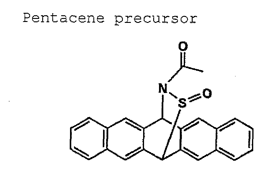
Subsequently, after an aqueous dispersion (BAYTRON P
produced by Bayer Co., Ltd.) of polystyrene sulfonic acid and
poly(ethylenedioxythiophene) was ejected onto source and
drain electrodes employing a piezo type ink jet, and a
patterning and a natural drying processes were carried out, a
heat treatment process was conducted in nitrogen gas
atmosphere at 70 °C for 10 minutes to form source electrode 6
and drain electrode 7 (Fig. 11 - c). An organic thin-film
transistor having channel length L = 20 µm (the present
invention Sample No. 1) was prepared by the above method.
The present invention Sample No. 2 was prepared,
similarly to the present invention Sample No. 1, except that
hexyl triethoxy silane was employed in place of methyl
triethoxy silane in the present invention Sample No. 1.
In a similar way, the present invention Sample No. 3 was
prepared, similarly to the present invention Sample No. 1,
except that trifluoromethylethyl triethoxy silane was
employed in place of methyl triethoxy silane. The present
invention Sample No. 4 was also prepared, similarly to the
present invention Sample No. 1, except that
methyltriisopropoxy titanium was employed in place of methyl
triethoxy silane.
An organic thin-film transistor which was not subjected
to atmospheric pressure plasma surface treatment (comparative
Sample No. 1) was further prepared.
Shown below are measured results of a contact angle
against pure water in the case of thin film Sample Nos. 1 - 4
in the present invention as well as in the case of not being
subjected to atmospheric pressure plasma surface treatment.
The measured values are based on 40 seconds after dropping
pure water on the samples.
| Sample No. 1 | 78° |
| Sample No. 2 | 85° |
| Sample No. 3 | 95° |
| Sample No. 4 | 76° |
| Comparative sample No. 1 | 43° |
Thin-film transistor Sample Nos. 1 - 4 of the present
invention exhibited good working property as a p-channel
enhancement type FET (field-effect transistor). The drain
current was measured by sweeping the gate bias voltage from
-20 V to +70 V when the drain bias voltage of each sample was
set to -60 V to measure the carrier mobility at a saturated
region. Measured results are shown in the following table.
| Sample No. | Silane or titanium compound | Carrier mobility (cm2/Vs) |
| Present invention No. 1 | methyl triethoxy silane | (0.25 |
| Present invention No. 2 | hexyl triethoxy silane | 0.28 |
| Present invention No. 3 | trifluoromethylethyl triethoxy silane | 0.35 |
| Present invention No. 4 | methyltriisopropoxy titanium | 0.24 |
| Comparative Sample No. 1 | in the case of not being subjected to atmospheric pressure plasma surface treatment | 0.15 |
It is to be understood via this table that the present
invention samples exhibit higher carrier mobility than the
comparative sample.
The present invention Sample Nos. 5 - 8 and comparative
Sample 2 were prepared, similarly to the present invention
Sample Nos. 1 - 4 and comparative Sample 1, except that the
following organic semiconductor material is employed in place
of the organic semiconductor material used in Sample Nos. 1 -
4 and comparative Sample 1 in Example 1.
Prepared is a chloroform solution of a regioregular
poly(3-hexylthiophene) (produced by Ardrich Co., Ltd.) which
has been purified to have a Zn or Ni content of not more than
10 ppm. After this solution was ejected employing a piezo
type ink jet, and a patterning and a drying process at room
temperature were carried out, a heat treatment process was
conducted in an N2 gas replaced atmosphere at 50 °C for 30
minutes. The thickness of poly(3-hexylthiophene) at the time
was 30 nm.
Thin-film transistor Sample Nos. 5 - 8 of the present
invention exhibited good working property as a p-channel
enhancement type FET (field-effect transistor). The carrier
mobility at saturated region was also measured. The results
are shown in the table.
| Sample No. | Silane or titanium compound | Carrier mobility (cm2/Vs) |
| Present invention No. 5 | methyl triethoxy silane | 0.031 |
| Present invention No. 6 | hexyl triethoxy silane | 0.037 |
| Present invention No. 7 | trifluoromethylethyl triethoxy silane | 0.043 |
| Present invention No. 8 | methyltriisopropoxy titanium | 0.030 |
| Comparative Sample No. 2 | in the case of not being subjected to atmospheric pressure plasma surface treatment | 0.022 |
A substrate before forming a semiconductor layer
thereon was prepared as described below.
Similarly to Example 1, after a gate insulating layer
(a 200 nm thick silicon oxide layer) was prepared by the
atmospheric pressure plasma method, a substrate is exposed to
excited discharge gas for 3 seconds to be pretreated by
introducing discharge gas (N2 : O2 = 99 : 1 by volume) into
an atmospheric pressure plasma discharge treatment apparatus
shown in Fig. 8 before forming thin film 4. Incidentally, a
high frequency power supply (frequency: 40 kHz) produced by
Haiden Laboratory Inc. was employed, and the discharge output
power was set to 10 W/cm2.
Similarly to Example 1, thin film 4 was subsequently formed.
Substrates were prepared, similarly to substrate 1
except that the material of reactive gas used for the
atmospheric pressure plasma method was replaced as shown in
Table 3.
A substrate was prepared, similarly to substrate 1
except that thin film 4 was not formed.
A substrate was prepared, similarly to substrate 1
except that thin film 4 was formed as described below.
After immersing a substrate in a 1 mM toluene solution
of octadecyltrichloro silane at 40 °C for 60 minutes, the
substrate was soaked in toluene for 3 minutes via ultrasonic
cleaning, and dried in the air at room temperature.
Pentacene purified via sublimation (produced by Ardrich
Co., Ltd.) was evaporated under a vacuum of 3 x 10⁻⁴ Pa onto
the substrate prepared as described above, whereby a 50 nm
thick organic semiconductor layer was formed. Similarly to
Example 1, source and drain electrodes were further formed
to prepare a sample.
The drain current was measured by sweeping the gate
bias voltage from +20 V to -70 V when the drain bias voltage
of each sample was set to -60 V to measure the carrier
mobility at a saturated region, and thus the ratio of maximum
and minimum values of the resulting drain current (being an
on/off ratio). The results are shown in the following table
below.
Similarly to Example 2, an organic semiconductor layer
containing a regioregular poly(3-hexylthiophene) was prepared
on each substrate prepared under the same conditions as in
Example 3. The evaluation was subsequently made, similarly
to Example 3. The results are shown in the right-hand column
of the table below.
| Substrate No. | Reactive gas | Contact angle (°) | Carrier mobility | on/off ratio | Carrier mobility | on/off |
| 1 | CH3Si(OC2H5)3 | 85 | 0.52 | 4.5x10⁶ | 0.042 | 5.2 |
| 2 | CH3(CH2)5Si(OC2H5)3 | 93 | 0.67 | 1.3x10⁷ | 0.052 | 8.6 |
| 3 | CF3(CH2)2Si(OC2H5) | 100 | 0.75 | 2.2x10⁷ | 0.062 | 1.7 |
| 4 | CH3Si(OC3H7)3 | 86 | 0.51 | 3.8x10⁶ | 0.044 | 4.3 |
| 5 | 7 | 0.12 | 9.2x10⁴ | 0.003 | 3.5 | |
| 6 | 78 | 0.37 | 8.7x10⁵ | 0.025 | 1.3x10⁴ |
A substrate was prepared similarly to Example 4 except
that thin film 4 was changed.
The apparatus in Fig. 9 is employed for forming thin
film 4, and materials, gas and output obtained via the
atmospheric pressure plasma method are further shown in a
figure. Gases A and B were introduced from supply port of
gas M and supply port of gas G, respectively. Herein, when
thin film 4 was formed on substrate 7, a discharging process
was carried out at a frequency of 13.56 MHz employing a high
frequency power supply produced by Pearl Kogyo Co., Ltd.
When thin film 4 was formed on substrates 8 - 12, a
discharging process was also carried out with a frequency of
50 kHz employing a high frequency power supply produced by
Shinko Electric Co., Ltd. The discharging time was set to 5
seconds for both cases.
Results of the samples measured similarly to Example 4 are
shown in the following table.
| Substrate No. | Gas A | Gas B | |||||||
| Silane compound or titanium compound | Discharge gas | Reactive gas | Discharge gas | Output power | |||||
| 7 | (CH3)2 Si (OC2H5) | 0.1vol% | Ar | 99.9 Vol% | H2 | 1.0 vol% | Ar | 99.0 vol% | 3W/cm2 |
| 8 | CF3(CF2)7CH2CH2Si(OCH3)3 vol% | 0.1 vol% | N2 | 99.9 Vol% | H2 | 1.0 vol% | N2 | 99.0 vol% | 5.5W/cm2 |
| 9 | CH3(CH2)17SiCl3 | 0.1 vol% | N2 | 99.9 vol% | H2 | 1.0 vol% | N2 | 99.0 vol% | 5.5W/cm2 |
| 10 | (CH3)3SiOSi(CH3)3 | 0.1 vol% | Ar | 99.9 vol% | H2 | 1.0 vol% | Ar | 99.0 vol% | 5.5W/cm2 |
| 11 | (C6H5)2Si(OCH3)2 | 0.1 vol% | Ar | 99.9 vol% | H2 | 1.0 vol% | Ar | 99.0 vol% | 5.5W/cm2 |
| 12 | OPTOOL DSX | 0.1 vol% | N2 | 99.9 vol% | H2 | 1.0 vol% | N2 | 99.0 vol% | 5.5W/cm2 |
| Substrate No. angle | Contact (°) | Carrier mobility | on/off |
| 7 | 95 | 0.053 | 9.1x10⁴ |
| 8 | 107 | 0.073 | 2.1x10⁵ |
| 9 | 93 | 0.048 | 5.5 |
| 10 | 96 | 0.055 | 9.3x10⁴ |
| 11 | 90 | 0.045 | 4.3x10⁴ |
| 12 | 112 | 0.076 | 1.8x10⁵ |
An organic thin-film transistor exhibiting high carrier
mobility and a manufacturing method thereof can be provided
via the present invention. An organic thin-film transistor
capable of providing mass production at low cost, and its
method suitable for manufacturing via a non vacuum system
roll-to-roll process can also be provided.
Claims (16)
- An organic thin-film transistor comprising a film having a contact angle against pure water of a surface of not less than 50°,
wherein an organic semiconductor layer is formed on the film prepared by a CVD (chemical vapor deposition) method employing a reactive gas. - The organic thin-film transistor of Claim 1,
wherein the aforesaid CVD method is a plasma CVD method. - The organic thin-film transistor of Claim 2,
wherein the aforesaid plasma CVD method is an atmospheric pressure plasma method in which discharge-plasma is generated by applying a high frequency voltage between electrodes facing each other at atmospheric pressure or approximately atmospheric pressure. - The organic thin-film transistor of any one of Claims 1 - 3,
wherein raw material of the reactive gas contains a silicon and/or fluorine-containing organic compound. - The organic thin-film transistor of any one of Claims 1 - 4,
wherein the raw material of the reactive gas contains a silane compound having at least one alkyl group, or a titanium compound having at least one alkyl group. - The organic thin-film transistor of any one of Claims 1 - 5,
wherein the organic semiconductor layer contains a π conjugate polymer or a π conjugate oligomer. - A method for manufacturing an organic thin-film transistor comprising a film having a contact angle against pure water of a surface of not less than 50°,
wherein an organic semiconductor layer is formed on the film provided on a gate insulating layer after the gate electrode and the gate insulating layer are formed on a substrate surface, which is prepared by a CVD (chemical vapor deposition) method employing the reactive gas. - The method for manufacturing the organic thin-film transistor of Claim 7,
wherein the aforesaid CVD method is a plasma CVD method. - The method for manufacturing the organic thin-film transistor of Claim 8,
wherein the aforesaid plasma CVD method is an atmospheric pressure plasma method in which discharge-plasma is generated by applying a high frequency voltage between electrodes facing each other at atmospheric pressure or approximately atmospheric pressure. - The method for manufacturing the organic thin-film transistor of any one of Claims 7 - 9,
wherein the aforesaid gate insulating layer is formed by generating discharge-plasma after a high frequency voltage is applied between electrodes facing each other at atmospheric pressure or approximately atmospheric pressure, and by placing the substrate, on which the gate electrode is formed, in reactive gas excited by the plasma. - The method for manufacturing the organic thin-film transistor of any one of Claims 7 - 10,
wherein the aforesaid film is formed after the gate insulating layer is placed in the generated discharge-plasma, supplying a discharge gas, by applying a high frequency voltage between electrodes facing each other at atmospheric pressure or approximately atmospheric pressure. - The method for manufacturing the organic thin-film transistor of Claim 11,
wherein the aforesaid discharge gas contains oxygen. - The method for manufacturing the organic thin-film transistor of any one of Claims 7 - 12,
wherein the raw material of the reactive gas for forming a film contains a silicon and/or fluorine-containing organic compound. - The method for manufacturing the organic thin-film transistor of any one of Claims 7 - 13,
wherein the raw material of the reactive gas for forming a film contains a silane compound having at least one alkyl group, or a titanium compound having at least one alkyl group. - The method for manufacturing the organic thin-film transistor of any one of Claims 7 - 14,
wherein a process for forming an organic semiconductor layer comprises a process for volatilizing a solvent in a solution after supplying the semiconducting material solution. - The method for manufacturing the organic thin-film transistor of Claim 15,
wherein the aforesaid semiconducting material contains a π conjugate polymer or a π conjugate oligomer.
Applications Claiming Priority (3)
| Application Number | Priority Date | Filing Date | Title |
|---|---|---|---|
| JP2003039535 | 2003-02-18 | ||
| JP2003039535 | 2003-02-18 | ||
| PCT/JP2004/001705 WO2004075279A1 (en) | 2003-02-18 | 2004-02-17 | Organic thin-film transistor device and method for manufacturing same |
Publications (2)
| Publication Number | Publication Date |
|---|---|
| EP1596428A1 true EP1596428A1 (en) | 2005-11-16 |
| EP1596428A4 EP1596428A4 (en) | 2008-12-24 |
Family
ID=32905173
Family Applications (1)
| Application Number | Title | Priority Date | Filing Date |
|---|---|---|---|
| EP04711711A Withdrawn EP1596428A4 (en) | 2003-02-18 | 2004-02-17 | Organic thin-film transistor device and method for manufacturing same |
Country Status (6)
| Country | Link |
|---|---|
| US (1) | US7645630B2 (en) |
| EP (1) | EP1596428A4 (en) |
| JP (2) | JP4892973B2 (en) |
| KR (1) | KR101129101B1 (en) |
| CN (1) | CN100501945C (en) |
| WO (1) | WO2004075279A1 (en) |
Cited By (3)
| Publication number | Priority date | Publication date | Assignee | Title |
|---|---|---|---|---|
| EP1496554A3 (en) * | 2003-07-07 | 2006-04-12 | Seiko Epson Corporation | Organic thin film transistor and method of manufacturing the same |
| EP1702963A1 (en) * | 2005-03-14 | 2006-09-20 | JDS Uniphase Corporation | Anti-moisture and soil-repellent coatings |
| EP2844781A4 (en) * | 2012-05-02 | 2016-01-13 | Basf Se | Method for the deposition of an organic material |
Families Citing this family (26)
| Publication number | Priority date | Publication date | Assignee | Title |
|---|---|---|---|---|
| EP1648040B1 (en) * | 2004-08-31 | 2016-06-01 | Osaka University | Thin-layer chemical transistors and their manufacture |
| JP2006187705A (en) * | 2005-01-05 | 2006-07-20 | Konica Minolta Holdings Inc | Method for forming organic semiconductor layer and method for producing organic thin film transistor |
| JP2006187706A (en) * | 2005-01-05 | 2006-07-20 | Konica Minolta Holdings Inc | Method for forming organic semiconductor layer and method for producing organic thin film transistor |
| US20060231829A1 (en) * | 2005-04-13 | 2006-10-19 | Xerox Corporation | TFT gate dielectric with crosslinked polymer |
| US7705346B2 (en) * | 2005-06-06 | 2010-04-27 | Xerox Corporation | Barrier layer for an organic electronic device |
| JP5055716B2 (en) * | 2005-06-08 | 2012-10-24 | コニカミノルタホールディングス株式会社 | Method for forming organic semiconductor film and method for producing organic thin film transistor |
| JP2007012986A (en) * | 2005-07-01 | 2007-01-18 | Univ Of Tokyo | Organic semiconductor device |
| KR100716148B1 (en) * | 2005-07-06 | 2007-05-10 | 양재우 | Synthesis method of compound used as organosilicon insulator |
| JP2007189961A (en) * | 2006-01-20 | 2007-08-02 | Toppan Printing Co Ltd | Container manufacturing method and surface treatment apparatus |
| US8138075B1 (en) | 2006-02-06 | 2012-03-20 | Eberlein Dietmar C | Systems and methods for the manufacture of flat panel devices |
| EP2001063A1 (en) * | 2006-03-24 | 2008-12-10 | Konica Minolta Holdings, Inc. | Organic semiconductor thin film, organic thin film transistor and method for manufacturing same |
| JP5055844B2 (en) * | 2006-06-05 | 2012-10-24 | コニカミノルタホールディングス株式会社 | Organic thin film transistor and method for producing organic thin film transistor |
| KR100886723B1 (en) * | 2007-02-20 | 2009-03-04 | 고려대학교 산학협력단 | Method for manufacturing organic thin film transistor and organic thin film transistor manufactured by the method |
| US7829375B2 (en) * | 2007-07-18 | 2010-11-09 | Konica Minolta Holdings, Inc. | Method for manufacturing organic thin film transistor and organic thin film transistor |
| JP2009117619A (en) * | 2007-11-06 | 2009-05-28 | Idemitsu Kosan Co Ltd | Organic thin film transistor manufacturing method and organic thin film transistor |
| JP5549754B2 (en) * | 2008-08-29 | 2014-07-16 | 東京エレクトロン株式会社 | Deposition equipment |
| KR101144233B1 (en) * | 2009-07-28 | 2012-05-10 | 지 . 텍 (주) | Method and Device For Pre-treatment of Roll-to-Roll Sputtering Apparatus |
| TWI557834B (en) * | 2010-04-09 | 2016-11-11 | 尼康股份有限公司 | Substrate processing device |
| JP5539081B2 (en) * | 2010-07-16 | 2014-07-02 | 株式会社カネカ | Manufacturing method of integrated thin film photoelectric conversion device |
| KR20190141027A (en) * | 2012-05-24 | 2019-12-20 | 가부시키가이샤 니콘 | Device manufacturing method |
| CN103604835A (en) * | 2013-12-09 | 2014-02-26 | 电子科技大学 | Preparation method of organic thin film transistor-based carbon monoxide gas sensor |
| JP5882510B2 (en) * | 2014-06-30 | 2016-03-09 | 太陽インキ製造株式会社 | Photosensitive dry film and method for producing printed wiring board using the same |
| KR102008566B1 (en) * | 2016-05-24 | 2019-08-07 | 가부시키가이샤 스크린 홀딩스 | Substrate processing apparatus and substrate processing method |
| KR102323894B1 (en) * | 2017-04-05 | 2021-11-08 | 이상인 | Deposition of Materials by Spraying of Precursors Using Supercritical Fluids |
| US10388895B2 (en) * | 2017-11-07 | 2019-08-20 | Shenzhen China Star Optoelectonics Semiconductor Display Technology Co., Ltd. | Organic thin film transistor with charge injection layer and manufacturing method thereof |
| EP3770948A4 (en) * | 2018-03-23 | 2021-12-29 | Kabushiki Kaisha Toshiba | Treatment solution and treatment method |
Family Cites Families (21)
| Publication number | Priority date | Publication date | Assignee | Title |
|---|---|---|---|---|
| US3754986A (en) * | 1969-08-18 | 1973-08-28 | Eastman Kodak Co | Organic semiconductors |
| JPS582032A (en) * | 1981-06-29 | 1983-01-07 | Fujitsu Ltd | Organic thin film formation |
| JPH0777273B2 (en) * | 1986-12-24 | 1995-08-16 | キヤノン株式会社 | Switching element and driving method thereof |
| US6107117A (en) | 1996-12-20 | 2000-08-22 | Lucent Technologies Inc. | Method of making an organic thin film transistor |
| JPH1129585A (en) | 1997-07-04 | 1999-02-02 | Shin Etsu Chem Co Ltd | Perfluoropolyether-modified aminosilane and surface treatment agent |
| US5936259A (en) | 1997-10-16 | 1999-08-10 | Lucent Technologies Inc. | Thin film transistor and organic semiconductor material thereof |
| TW399338B (en) | 1997-11-24 | 2000-07-21 | Lucent Technologies Inc | Method of making an organic thin film transistor and article made by the method |
| JP4733798B2 (en) | 1998-01-31 | 2011-07-27 | 凸版印刷株式会社 | Antifouling agent, method for forming antifouling layer, optical member, antireflection optical member, optical functional member, and display device |
| US6159871A (en) * | 1998-05-29 | 2000-12-12 | Dow Corning Corporation | Method for producing hydrogenated silicon oxycarbide films having low dielectric constant |
| JP2000064348A (en) | 1998-08-26 | 2000-02-29 | Hitachi Constr Mach Co Ltd | Construction equipment |
| US6399270B1 (en) * | 1998-12-04 | 2002-06-04 | Konica Corporation | Support for printing plate and printing plate |
| JP2000269504A (en) * | 1999-03-16 | 2000-09-29 | Hitachi Ltd | Semiconductor device, manufacturing method thereof, and liquid crystal display device |
| US6265243B1 (en) | 1999-03-29 | 2001-07-24 | Lucent Technologies Inc. | Process for fabricating organic circuits |
| JP2001094107A (en) * | 1999-09-20 | 2001-04-06 | Hitachi Ltd | Organic semiconductor device and liquid crystal display |
| AU779878B2 (en) * | 1999-12-21 | 2005-02-17 | Flexenable Limited | Forming interconnects |
| JP2001244467A (en) | 2000-02-28 | 2001-09-07 | Hitachi Ltd | Coplanar semiconductor device, display device and manufacturing method using the same |
| JP2002151508A (en) * | 2000-11-15 | 2002-05-24 | Sekisui Chem Co Ltd | Semiconductor device manufacturing method and apparatus |
| JP2003049272A (en) * | 2001-08-07 | 2003-02-21 | Konica Corp | Atmospheric pressure plasma treating device, atmospheric pressure plasma treating method and electrode system for atmospheric pressure plasma treating device |
| EP1291932A3 (en) * | 2001-09-05 | 2006-10-18 | Konica Corporation | Organic thin-film semiconductor element and manufacturing method for the same |
| US6740900B2 (en) * | 2002-02-27 | 2004-05-25 | Konica Corporation | Organic thin-film transistor and manufacturing method for the same |
| EP1434282A3 (en) * | 2002-12-26 | 2007-06-27 | Konica Minolta Holdings, Inc. | Protective layer for an organic thin-film transistor |
-
2004
- 2004-02-17 WO PCT/JP2004/001705 patent/WO2004075279A1/en not_active Ceased
- 2004-02-17 EP EP04711711A patent/EP1596428A4/en not_active Withdrawn
- 2004-02-17 KR KR1020057014875A patent/KR101129101B1/en not_active Expired - Fee Related
- 2004-02-17 JP JP2005502705A patent/JP4892973B2/en not_active Expired - Fee Related
- 2004-02-17 US US10/545,361 patent/US7645630B2/en not_active Expired - Fee Related
- 2004-02-17 CN CNB2004800042259A patent/CN100501945C/en not_active Expired - Fee Related
-
2010
- 2010-06-02 JP JP2010126609A patent/JP2010265548A/en active Pending
Cited By (4)
| Publication number | Priority date | Publication date | Assignee | Title |
|---|---|---|---|---|
| EP1496554A3 (en) * | 2003-07-07 | 2006-04-12 | Seiko Epson Corporation | Organic thin film transistor and method of manufacturing the same |
| US7329897B2 (en) | 2003-07-07 | 2008-02-12 | Seiko Epson Corporation | Organic thin film transistor and method of manufacturing the same |
| EP1702963A1 (en) * | 2005-03-14 | 2006-09-20 | JDS Uniphase Corporation | Anti-moisture and soil-repellent coatings |
| EP2844781A4 (en) * | 2012-05-02 | 2016-01-13 | Basf Se | Method for the deposition of an organic material |
Also Published As
| Publication number | Publication date |
|---|---|
| CN100501945C (en) | 2009-06-17 |
| CN1751385A (en) | 2006-03-22 |
| WO2004075279A1 (en) | 2004-09-02 |
| JP2010265548A (en) | 2010-11-25 |
| US7645630B2 (en) | 2010-01-12 |
| US20060131561A1 (en) | 2006-06-22 |
| EP1596428A4 (en) | 2008-12-24 |
| JPWO2004075279A1 (en) | 2006-06-01 |
| KR20050096188A (en) | 2005-10-05 |
| KR101129101B1 (en) | 2012-03-23 |
| JP4892973B2 (en) | 2012-03-07 |
Similar Documents
| Publication | Publication Date | Title |
|---|---|---|
| US7645630B2 (en) | Manufacturing method for thin-film transistor | |
| EP1291932A2 (en) | Organic thin-film semiconductor element and manufacturing method for the same | |
| JP5054885B2 (en) | Organic thin-film transistor including multi-layer gate insulating film | |
| KR101880838B1 (en) | Hybrid dielectric material for thin film transistors | |
| US20080197349A1 (en) | Manufacturing method of thin-film transistor, thin film transistor sheet, and electric circuit | |
| US7785948B2 (en) | Semiconductor element and process for producing the same | |
| US20110068332A1 (en) | Hybrid Dielectric Material for Thin Film Transistors | |
| JP2008171978A (en) | Organic thin film transistor | |
| EP2117059B1 (en) | Organic Thin Film Transistors | |
| JP2003179234A (en) | Organic semiconductor device and method of manufacturing the same | |
| JP4254123B2 (en) | Organic thin film transistor and manufacturing method thereof | |
| JP2004152959A (en) | Organic thin-film transistor, organic thin-film transistor sheet, and manufacturing method thereof | |
| US8106387B2 (en) | Organic thin film transistors | |
| US7829375B2 (en) | Method for manufacturing organic thin film transistor and organic thin film transistor | |
| WO2006033282A1 (en) | Thin film transistor and thin film transistor element sheet, and method for fabricating thin film transistor and thin film transistor element sheet | |
| JP2004281477A (en) | Organic thin film transistor and method of manufacturing the same | |
| JPWO2008090828A1 (en) | Organic thin film transistor, manufacturing method thereof, and organic semiconductor device | |
| JP2004128124A (en) | Organic thin film transistor and method of manufacturing organic thin film transistor | |
| WO2010082414A1 (en) | Organic thin film transistor, method for manufacturing same, and device equipped with same | |
| JP4345317B2 (en) | Organic thin film transistor element | |
| JP2004207331A (en) | Organic semiconductor device and method of manufacturing the same | |
| WO2007029551A1 (en) | Organic thin film transistor, base body for organic thin film transistor and method for manufacturing organic thin film transistor | |
| JP2010056115A (en) | Method of forming gate insulating film, method of manufacturing organic thin-film transistor, and organic thin-film device | |
| WO2007125899A1 (en) | Organic thin-film transistor | |
| JP2008060115A (en) | Manufacturing method of organic thin film transistor and organic thin film transistor manufactured by the manufacturing method |
Legal Events
| Date | Code | Title | Description |
|---|---|---|---|
| PUAI | Public reference made under article 153(3) epc to a published international application that has entered the european phase |
Free format text: ORIGINAL CODE: 0009012 |
|
| 17P | Request for examination filed |
Effective date: 20050811 |
|
| AK | Designated contracting states |
Kind code of ref document: A1 Designated state(s): AT BE BG CH CY CZ DE DK EE ES FI FR GB GR HU IE IT LI LU MC NL PT RO SE SI SK TR |
|
| AX | Request for extension of the european patent |
Extension state: AL LT LV MK |
|
| A4 | Supplementary search report drawn up and despatched |
Effective date: 20081124 |
|
| 17Q | First examination report despatched |
Effective date: 20090327 |
|
| STAA | Information on the status of an ep patent application or granted ep patent |
Free format text: STATUS: THE APPLICATION IS DEEMED TO BE WITHDRAWN |
|
| 18D | Application deemed to be withdrawn |
Effective date: 20101019 |