EP1593293B1 - Kombinierte metall- und kunststoff-emi-abschirmung - Google Patents
Kombinierte metall- und kunststoff-emi-abschirmung Download PDFInfo
- Publication number
- EP1593293B1 EP1593293B1 EP04705236A EP04705236A EP1593293B1 EP 1593293 B1 EP1593293 B1 EP 1593293B1 EP 04705236 A EP04705236 A EP 04705236A EP 04705236 A EP04705236 A EP 04705236A EP 1593293 B1 EP1593293 B1 EP 1593293B1
- Authority
- EP
- European Patent Office
- Prior art keywords
- shield
- electrically
- conductive
- assembly
- metal
- Prior art date
- Legal status (The legal status is an assumption and is not a legal conclusion. Google has not performed a legal analysis and makes no representation as to the accuracy of the status listed.)
- Expired - Lifetime
Links
- 229910052751 metal Inorganic materials 0.000 title claims abstract description 35
- 239000002184 metal Substances 0.000 title claims abstract description 35
- 229920003023 plastic Polymers 0.000 title abstract description 12
- 239000004033 plastic Substances 0.000 title abstract description 12
- 239000000945 filler Substances 0.000 claims abstract description 19
- 239000002131 composite material Substances 0.000 claims abstract description 13
- 239000000835 fiber Substances 0.000 claims description 18
- OKTJSMMVPCPJKN-UHFFFAOYSA-N Carbon Chemical compound [C] OKTJSMMVPCPJKN-UHFFFAOYSA-N 0.000 claims description 17
- 239000000203 mixture Substances 0.000 claims description 17
- -1 polybutylene terephthalates Polymers 0.000 claims description 16
- 239000010439 graphite Substances 0.000 claims description 10
- 229910002804 graphite Inorganic materials 0.000 claims description 10
- 229910052782 aluminium Inorganic materials 0.000 claims description 9
- XAGFODPZIPBFFR-UHFFFAOYSA-N aluminium Chemical compound [Al] XAGFODPZIPBFFR-UHFFFAOYSA-N 0.000 claims description 9
- 229910052799 carbon Inorganic materials 0.000 claims description 7
- 229920001577 copolymer Polymers 0.000 claims description 7
- 239000000956 alloy Substances 0.000 claims description 6
- 229920001940 conductive polymer Polymers 0.000 claims description 6
- 229910052755 nonmetal Inorganic materials 0.000 claims description 6
- 229920005989 resin Polymers 0.000 claims description 6
- 239000011347 resin Substances 0.000 claims description 6
- 239000012799 electrically-conductive coating Substances 0.000 claims description 5
- 229920001169 thermoplastic Polymers 0.000 claims description 5
- FYYHWMGAXLPEAU-UHFFFAOYSA-N Magnesium Chemical compound [Mg] FYYHWMGAXLPEAU-UHFFFAOYSA-N 0.000 claims description 4
- 239000004952 Polyamide Substances 0.000 claims description 4
- 239000004642 Polyimide Substances 0.000 claims description 4
- 239000004793 Polystyrene Substances 0.000 claims description 4
- 229910000831 Steel Inorganic materials 0.000 claims description 4
- 229920000122 acrylonitrile butadiene styrene Polymers 0.000 claims description 4
- 229910045601 alloy Inorganic materials 0.000 claims description 4
- 229910052749 magnesium Inorganic materials 0.000 claims description 4
- 239000011777 magnesium Substances 0.000 claims description 4
- 150000002739 metals Chemical class 0.000 claims description 4
- 229920001778 nylon Polymers 0.000 claims description 4
- 229920002647 polyamide Polymers 0.000 claims description 4
- 229920000728 polyester Polymers 0.000 claims description 4
- 229920001721 polyimide Polymers 0.000 claims description 4
- 229920002223 polystyrene Polymers 0.000 claims description 4
- 229920000915 polyvinyl chloride Polymers 0.000 claims description 4
- 239000010959 steel Substances 0.000 claims description 4
- 229920001187 thermosetting polymer Polymers 0.000 claims description 4
- 239000004593 Epoxy Substances 0.000 claims description 3
- 229920000106 Liquid crystal polymer Polymers 0.000 claims description 3
- 239000004977 Liquid-crystal polymers (LCPs) Substances 0.000 claims description 3
- 229920002319 Poly(methyl acrylate) Polymers 0.000 claims description 3
- 239000004721 Polyphenylene oxide Substances 0.000 claims description 3
- HCHKCACWOHOZIP-UHFFFAOYSA-N Zinc Chemical compound [Zn] HCHKCACWOHOZIP-UHFFFAOYSA-N 0.000 claims description 3
- 150000001241 acetals Chemical class 0.000 claims description 3
- XECAHXYUAAWDEL-UHFFFAOYSA-N acrylonitrile butadiene styrene Chemical compound C=CC=C.C=CC#N.C=CC1=CC=CC=C1 XECAHXYUAAWDEL-UHFFFAOYSA-N 0.000 claims description 3
- 125000003700 epoxy group Chemical group 0.000 claims description 3
- 229920002313 fluoropolymer Polymers 0.000 claims description 3
- 239000004811 fluoropolymer Substances 0.000 claims description 3
- 229920002492 poly(sulfone) Polymers 0.000 claims description 3
- 229920001707 polybutylene terephthalate Polymers 0.000 claims description 3
- 239000004417 polycarbonate Substances 0.000 claims description 3
- 229920000515 polycarbonate Polymers 0.000 claims description 3
- 229920000647 polyepoxide Polymers 0.000 claims description 3
- 229920002530 polyetherether ketone Polymers 0.000 claims description 3
- 229920001601 polyetherimide Polymers 0.000 claims description 3
- 229920000139 polyethylene terephthalate Polymers 0.000 claims description 3
- 229920000098 polyolefin Polymers 0.000 claims description 3
- 235000013824 polyphenols Nutrition 0.000 claims description 3
- 229920001955 polyphenylene ether Polymers 0.000 claims description 3
- 229920006380 polyphenylene oxide Polymers 0.000 claims description 3
- 239000011701 zinc Substances 0.000 claims description 3
- 229910052725 zinc Inorganic materials 0.000 claims description 3
- 229920002635 polyurethane Polymers 0.000 claims description 2
- 239000004814 polyurethane Substances 0.000 claims description 2
- DHKHKXVYLBGOIT-UHFFFAOYSA-N acetaldehyde Diethyl Acetal Natural products CCOC(C)OCC DHKHKXVYLBGOIT-UHFFFAOYSA-N 0.000 claims 2
- 239000004676 acrylonitrile butadiene styrene Substances 0.000 claims 2
- 150000002148 esters Chemical class 0.000 claims 2
- RTZKZFJDLAIYFH-UHFFFAOYSA-N ether Substances CCOCC RTZKZFJDLAIYFH-UHFFFAOYSA-N 0.000 claims 2
- 229920001519 homopolymer Polymers 0.000 claims 2
- 239000000463 material Substances 0.000 description 18
- PXHVJJICTQNCMI-UHFFFAOYSA-N Nickel Chemical compound [Ni] PXHVJJICTQNCMI-UHFFFAOYSA-N 0.000 description 12
- 239000011248 coating agent Substances 0.000 description 10
- 238000000576 coating method Methods 0.000 description 10
- 239000010410 layer Substances 0.000 description 10
- 238000010276 construction Methods 0.000 description 9
- 238000000034 method Methods 0.000 description 8
- 229910052759 nickel Inorganic materials 0.000 description 6
- 239000000126 substance Substances 0.000 description 6
- WBTMFEPLVQOWFI-UHFFFAOYSA-N 1,3-dichloro-5-(2,5-dichlorophenyl)benzene Chemical compound ClC1=CC=C(Cl)C(C=2C=C(Cl)C=C(Cl)C=2)=C1 WBTMFEPLVQOWFI-UHFFFAOYSA-N 0.000 description 5
- 150000001875 compounds Chemical class 0.000 description 5
- 239000002245 particle Substances 0.000 description 5
- 230000008569 process Effects 0.000 description 5
- RYGMFSIKBFXOCR-UHFFFAOYSA-N Copper Chemical compound [Cu] RYGMFSIKBFXOCR-UHFFFAOYSA-N 0.000 description 4
- 239000000654 additive Substances 0.000 description 4
- 229910052802 copper Inorganic materials 0.000 description 4
- 239000010949 copper Substances 0.000 description 4
- 238000009472 formulation Methods 0.000 description 4
- 239000011521 glass Substances 0.000 description 4
- PCHJSUWPFVWCPO-UHFFFAOYSA-N gold Chemical compound [Au] PCHJSUWPFVWCPO-UHFFFAOYSA-N 0.000 description 4
- 229910052737 gold Inorganic materials 0.000 description 4
- 239000010931 gold Substances 0.000 description 4
- 238000000465 moulding Methods 0.000 description 4
- 229920000642 polymer Polymers 0.000 description 4
- 229910052709 silver Inorganic materials 0.000 description 4
- 239000004332 silver Substances 0.000 description 4
- 229920002943 EPDM rubber Polymers 0.000 description 3
- BQCADISMDOOEFD-UHFFFAOYSA-N Silver Chemical compound [Ag] BQCADISMDOOEFD-UHFFFAOYSA-N 0.000 description 3
- ATJFFYVFTNAWJD-UHFFFAOYSA-N Tin Chemical compound [Sn] ATJFFYVFTNAWJD-UHFFFAOYSA-N 0.000 description 3
- 239000000853 adhesive Substances 0.000 description 3
- 230000001070 adhesive effect Effects 0.000 description 3
- 230000001413 cellular effect Effects 0.000 description 3
- 238000004891 communication Methods 0.000 description 3
- 229920001971 elastomer Polymers 0.000 description 3
- 238000004519 manufacturing process Methods 0.000 description 3
- 229910000510 noble metal Inorganic materials 0.000 description 3
- 150000002843 nonmetals Chemical class 0.000 description 3
- 239000008188 pellet Substances 0.000 description 3
- 229920001296 polysiloxane Polymers 0.000 description 3
- 229920003048 styrene butadiene rubber Polymers 0.000 description 3
- 239000004416 thermosoftening plastic Substances 0.000 description 3
- 229910052718 tin Inorganic materials 0.000 description 3
- 229910000838 Al alloy Inorganic materials 0.000 description 2
- KAKZBPTYRLMSJV-UHFFFAOYSA-N Butadiene Chemical compound C=CC=C KAKZBPTYRLMSJV-UHFFFAOYSA-N 0.000 description 2
- JOYRKODLDBILNP-UHFFFAOYSA-N Ethyl urethane Chemical compound CCOC(N)=O JOYRKODLDBILNP-UHFFFAOYSA-N 0.000 description 2
- 229920000459 Nitrile rubber Polymers 0.000 description 2
- VYPSYNLAJGMNEJ-UHFFFAOYSA-N Silicium dioxide Chemical class O=[Si]=O VYPSYNLAJGMNEJ-UHFFFAOYSA-N 0.000 description 2
- 239000002174 Styrene-butadiene Substances 0.000 description 2
- ADCOVFLJGNWWNZ-UHFFFAOYSA-N antimony trioxide Chemical compound O=[Sb]O[Sb]=O ADCOVFLJGNWWNZ-UHFFFAOYSA-N 0.000 description 2
- 239000011230 binding agent Substances 0.000 description 2
- MTAZNLWOLGHBHU-UHFFFAOYSA-N butadiene-styrene rubber Chemical class C=CC=C.C=CC1=CC=CC=C1 MTAZNLWOLGHBHU-UHFFFAOYSA-N 0.000 description 2
- 239000000919 ceramic Substances 0.000 description 2
- 239000003795 chemical substances by application Substances 0.000 description 2
- 239000011231 conductive filler Substances 0.000 description 2
- 239000004020 conductor Substances 0.000 description 2
- 239000000470 constituent Substances 0.000 description 2
- 238000004132 cross linking Methods 0.000 description 2
- 230000000694 effects Effects 0.000 description 2
- 230000005670 electromagnetic radiation Effects 0.000 description 2
- 239000004744 fabric Substances 0.000 description 2
- 230000013011 mating Effects 0.000 description 2
- 239000010445 mica Substances 0.000 description 2
- 229910052618 mica group Inorganic materials 0.000 description 2
- 239000004005 microsphere Substances 0.000 description 2
- CWQXQMHSOZUFJS-UHFFFAOYSA-N molybdenum disulfide Chemical compound S=[Mo]=S CWQXQMHSOZUFJS-UHFFFAOYSA-N 0.000 description 2
- 229910052982 molybdenum disulfide Inorganic materials 0.000 description 2
- 150000002825 nitriles Chemical class 0.000 description 2
- 239000003973 paint Substances 0.000 description 2
- 239000000049 pigment Substances 0.000 description 2
- 229920001084 poly(chloroprene) Polymers 0.000 description 2
- 229920001200 poly(ethylene-vinyl acetate) Polymers 0.000 description 2
- 239000000843 powder Substances 0.000 description 2
- 230000005855 radiation Effects 0.000 description 2
- 239000005060 rubber Substances 0.000 description 2
- 229910000679 solder Inorganic materials 0.000 description 2
- 239000007787 solid Substances 0.000 description 2
- 229920000468 styrene butadiene styrene block copolymer Polymers 0.000 description 2
- VSKJLJHPAFKHBX-UHFFFAOYSA-N 2-methylbuta-1,3-diene;styrene Chemical class CC(=C)C=C.C=CC1=CC=CC=C1.C=CC1=CC=CC=C1 VSKJLJHPAFKHBX-UHFFFAOYSA-N 0.000 description 1
- 229920000742 Cotton Polymers 0.000 description 1
- 244000043261 Hevea brasiliensis Species 0.000 description 1
- 229910000792 Monel Inorganic materials 0.000 description 1
- 239000004677 Nylon Substances 0.000 description 1
- 229910019142 PO4 Inorganic materials 0.000 description 1
- 239000004820 Pressure-sensitive adhesive Substances 0.000 description 1
- 229920006397 acrylic thermoplastic Polymers 0.000 description 1
- RREGISFBPQOLTM-UHFFFAOYSA-N alumane;trihydrate Chemical compound O.O.O.[AlH3] RREGISFBPQOLTM-UHFFFAOYSA-N 0.000 description 1
- 230000003466 anti-cipated effect Effects 0.000 description 1
- 239000002518 antifoaming agent Substances 0.000 description 1
- 239000003963 antioxidant agent Substances 0.000 description 1
- 239000002216 antistatic agent Substances 0.000 description 1
- 230000004888 barrier function Effects 0.000 description 1
- 239000011324 bead Substances 0.000 description 1
- 229910052797 bismuth Inorganic materials 0.000 description 1
- JCXGWMGPZLAOME-UHFFFAOYSA-N bismuth atom Chemical compound [Bi] JCXGWMGPZLAOME-UHFFFAOYSA-N 0.000 description 1
- 150000001642 boronic acid derivatives Chemical class 0.000 description 1
- FACXGONDLDSNOE-UHFFFAOYSA-N buta-1,3-diene;styrene Chemical class C=CC=C.C=CC1=CC=CC=C1.C=CC1=CC=CC=C1 FACXGONDLDSNOE-UHFFFAOYSA-N 0.000 description 1
- 125000000484 butyl group Chemical group [H]C([*])([H])C([H])([H])C([H])([H])C([H])([H])[H] 0.000 description 1
- 229920002678 cellulose Polymers 0.000 description 1
- 239000001913 cellulose Substances 0.000 description 1
- 238000005229 chemical vapour deposition Methods 0.000 description 1
- XTHPWXDJESJLNJ-UHFFFAOYSA-M chlorosulfate Chemical compound [O-]S(Cl)(=O)=O XTHPWXDJESJLNJ-UHFFFAOYSA-M 0.000 description 1
- 238000005253 cladding Methods 0.000 description 1
- 239000011247 coating layer Substances 0.000 description 1
- 239000003086 colorant Substances 0.000 description 1
- 238000007906 compression Methods 0.000 description 1
- 230000006835 compression Effects 0.000 description 1
- 238000001816 cooling Methods 0.000 description 1
- 239000007822 coupling agent Substances 0.000 description 1
- WHHGLZMJPXIBIX-UHFFFAOYSA-N decabromodiphenyl ether Chemical compound BrC1=C(Br)C(Br)=C(Br)C(Br)=C1OC1=C(Br)C(Br)=C(Br)C(Br)=C1Br WHHGLZMJPXIBIX-UHFFFAOYSA-N 0.000 description 1
- 238000007598 dipping method Methods 0.000 description 1
- 239000002270 dispersing agent Substances 0.000 description 1
- 238000009826 distribution Methods 0.000 description 1
- 238000001035 drying Methods 0.000 description 1
- 239000000975 dye Substances 0.000 description 1
- 239000000806 elastomer Substances 0.000 description 1
- 238000007772 electroless plating Methods 0.000 description 1
- 238000009713 electroplating Methods 0.000 description 1
- 239000003995 emulsifying agent Substances 0.000 description 1
- 230000007613 environmental effect Effects 0.000 description 1
- HDERJYVLTPVNRI-UHFFFAOYSA-N ethene;ethenyl acetate Chemical class C=C.CC(=O)OC=C HDERJYVLTPVNRI-UHFFFAOYSA-N 0.000 description 1
- 238000001704 evaporation Methods 0.000 description 1
- 230000008020 evaporation Effects 0.000 description 1
- 238000001125 extrusion Methods 0.000 description 1
- 238000011049 filling Methods 0.000 description 1
- 239000003063 flame retardant Substances 0.000 description 1
- 239000006260 foam Substances 0.000 description 1
- 238000005187 foaming Methods 0.000 description 1
- 239000004088 foaming agent Substances 0.000 description 1
- 239000011888 foil Substances 0.000 description 1
- 230000004927 fusion Effects 0.000 description 1
- 230000008676 import Effects 0.000 description 1
- 238000011065 in-situ storage Methods 0.000 description 1
- 229910052738 indium Inorganic materials 0.000 description 1
- APFVFJFRJDLVQX-UHFFFAOYSA-N indium atom Chemical compound [In] APFVFJFRJDLVQX-UHFFFAOYSA-N 0.000 description 1
- 238000002347 injection Methods 0.000 description 1
- 239000007924 injection Substances 0.000 description 1
- 238000010030 laminating Methods 0.000 description 1
- 238000011068 loading method Methods 0.000 description 1
- 239000000314 lubricant Substances 0.000 description 1
- 239000011159 matrix material Substances 0.000 description 1
- 229910044991 metal oxide Inorganic materials 0.000 description 1
- 150000004706 metal oxides Chemical class 0.000 description 1
- 230000000116 mitigating effect Effects 0.000 description 1
- 238000002156 mixing Methods 0.000 description 1
- 239000003607 modifier Substances 0.000 description 1
- 229920005690 natural copolymer Polymers 0.000 description 1
- 229920003052 natural elastomer Polymers 0.000 description 1
- 229920001194 natural rubber Polymers 0.000 description 1
- 239000003921 oil Substances 0.000 description 1
- 238000010422 painting Methods 0.000 description 1
- 238000005192 partition Methods 0.000 description 1
- 150000002978 peroxides Chemical class 0.000 description 1
- 235000021317 phosphate Nutrition 0.000 description 1
- 150000003013 phosphoric acid derivatives Chemical class 0.000 description 1
- 150000003014 phosphoric acid esters Chemical class 0.000 description 1
- 230000000704 physical effect Effects 0.000 description 1
- 229920003229 poly(methyl methacrylate) Polymers 0.000 description 1
- 229920002857 polybutadiene Polymers 0.000 description 1
- 229920001195 polyisoprene Polymers 0.000 description 1
- 239000002861 polymer material Substances 0.000 description 1
- 238000006116 polymerization reaction Methods 0.000 description 1
- 230000000379 polymerizing effect Effects 0.000 description 1
- 239000004800 polyvinyl chloride Substances 0.000 description 1
- 150000003839 salts Chemical class 0.000 description 1
- 238000007650 screen-printing Methods 0.000 description 1
- 150000004756 silanes Chemical class 0.000 description 1
- 150000004760 silicates Chemical class 0.000 description 1
- 239000000377 silicon dioxide Chemical class 0.000 description 1
- 125000006850 spacer group Chemical group 0.000 description 1
- 238000001228 spectrum Methods 0.000 description 1
- 238000005507 spraying Methods 0.000 description 1
- 239000003381 stabilizer Substances 0.000 description 1
- 239000011115 styrene butadiene Substances 0.000 description 1
- XTHPWXDJESJLNJ-UHFFFAOYSA-N sulfurochloridic acid Chemical class OS(Cl)(=O)=O XTHPWXDJESJLNJ-UHFFFAOYSA-N 0.000 description 1
- 239000004094 surface-active agent Substances 0.000 description 1
- 229920002994 synthetic fiber Polymers 0.000 description 1
- 239000012209 synthetic fiber Substances 0.000 description 1
- ISXSCDLOGDJUNJ-UHFFFAOYSA-N tert-butyl prop-2-enoate Chemical compound CC(C)(C)OC(=O)C=C ISXSCDLOGDJUNJ-UHFFFAOYSA-N 0.000 description 1
- 239000012815 thermoplastic material Substances 0.000 description 1
- 239000002562 thickening agent Substances 0.000 description 1
- 239000011135 tin Substances 0.000 description 1
- 238000010023 transfer printing Methods 0.000 description 1
- 238000001771 vacuum deposition Methods 0.000 description 1
- 239000000080 wetting agent Substances 0.000 description 1
- 210000002268 wool Anatomy 0.000 description 1
Images


Classifications
-
- H—ELECTRICITY
- H05—ELECTRIC TECHNIQUES NOT OTHERWISE PROVIDED FOR
- H05K—PRINTED CIRCUITS; CASINGS OR CONSTRUCTIONAL DETAILS OF ELECTRIC APPARATUS; MANUFACTURE OF ASSEMBLAGES OF ELECTRICAL COMPONENTS
- H05K9/00—Screening of apparatus or components against electric or magnetic fields
- H05K9/0007—Casings
- H05K9/002—Casings with localised screening
- H05K9/0022—Casings with localised screening of components mounted on printed circuit boards [PCB]
- H05K9/0024—Shield cases mounted on a PCB, e.g. cans or caps or conformal shields
- H05K9/0032—Shield cases mounted on a PCB, e.g. cans or caps or conformal shields having multiple parts, e.g. frames mating with lids
Definitions
- the present invention relates broadly to electromagnetic interference (EMI) shields, such as cases, housings, or parts thereof such as covers, or board-level shields such as single or multi-compartment covers or "cans," for mobile, i.e., cellular telephone handsets, telecommunication base stations, and other electronic devices, and particularly to a shield having a thin metal base portion to which is joined a wall portion formed of a conductive plastic or other polymeric material that may be molded or otherwise formed into a myriad of shapes.
- EMI electromagnetic interference
- shielding having the capability of absorbing and/or reflecting EMI energy may be employed both to confine the EMI energy within a source device, and to insulate that device or other "target" devices from other source devices.
- Such shielding is provided as a barrier which is interposed between the source and the other devices, and typically is configured as an electrically conductive and grounded housing which encloses the device, or as a "can" which covers a discrete component or componentry of the device.
- the housing or can may be formed of a metal such as steel, aluminum, or magnesium, or alternatively, of a plastic or other polymeric material which is filled to be electrically-conductive, such as is described in U.S. Pat. Nos.
- the coating may be an electrically-conductive paint, a conductively-filled, molded elastomeric layer, a metal foil laminate or transfer, or a flame-sprayed or other deposited metal layer.
- a conductive gasket may be used to provide electrical continuity between the coating layers applied to the various mating housing parts.
- JP19970133170 discloses a structure for a highfrequency shield case which can reduce the number of attached members and have a sufficient shielding effect.
- the shield includes a body formed from an electronically and thermally conductive composite material.
- stamped aluminum shield constructions are widely known and can be fabricated having very thin wall, i.e., z-axis, thicknesses of 0.2 mm or less, but are relatively expensive and difficult to fabricate in a cost-effective manner into the complex shapes which may be required for certain applications.
- conductively-filled plastics may be economically molded or otherwise formed into a variety of complex shapes, but generally cannot be used in shielding applications where very thin wall thicknesses are required in certain sections of the shield.
- the present invention relates broadly to electromagnetic interference (EMI) shields, such as cases, housings, or parts thereof such as covers, or board-level shields such as multi-or single-compartment covers or "cans," for mobile, i.e., cellular telephone handsets, telecommunication base stations, and other electronic devices. More particularly, the invention relates to a shield having a thin metal base section to which is joined a wall section formed of a conductively-filled plastic or other polymeric composite material that may be molded or otherwise formed into a myriad of shapes.
- EMI electromagnetic interference
- the shield is configured as a board-level cover or can for an electronic device, and has multiple compartments for shielding the circuitry of the device.
- the wall section is configured to define the multiple compartments, and may be molded, such as by means of insert molding, onto the base section to form an integral shield.
- the shield may be attached to the board, such as with an end surface of the wall section being in contact with a grounding trace formed on the board, using fasteners, clips, or other mechanical means.
- the shield may be soldered or adhesively bonded to the board.
- An electrically-conductive coating or elastomeric gasket also may be interposed between the wall section of the shield and the board to improve the electrical contact therebetween.
- the shield of the invention allows for a more economical construction as compared to metal stampings, while offering the designer the ability to fabricate shields having complex shapes but which still offer the thinner z-axis profiles which are attainable by the use of sheet metals.
- the precepts of the present invention are described in connection with the construction of a multi-compartment combination metal and plastic cover or "can" which is mountable onto or over a PCB for enclosing various circuitry sections of the PCB which itself may be received with the shield within a housing, case, or other enclosure of an electronic device such as a mobile, i.e., cellular, telephone handset, or other electronics device such as a personal communications services (PCS) handset, PCMCIA card, global positioning system (GPS), radio receiver, personal digital assistant (PDA), notebook or desktop personal computer (PC), cordless telephone handset, network router or server, medical electronics device, modern, wirelss communication base station, telemetry device, telematic component or system, or the like.
- PCS personal communications services
- PCMCIA card global positioning system
- GPS global positioning system
- PDA personal digital assistant
- PC notebook or desktop personal computer
- cordless telephone handset network router or server
- medical electronics device modern, wirelss communication base station, telemetry device, telematic component or
- EMI shielding should be understood to include, and to be used interchangeably with, electromagnetic compatibility (EMC), surface grounding, corona shielding, radio frequency interference (RFI) shielding, and anti-static, i.e., electro-static discharge (ESD) protection.
- EMC electromagnetic compatibility
- RFID radio frequency interference
- ESD electro-static discharge
- the shield alternatively may be configured as a single compartment can, or as another cover or housing of the device, or as configured for mounting to or contact with another part of the device which may be another shield, a cover or housing part, or a spacer gasket or other structure.
- aspects of the present invention also may find utility in other EMI shielding applications, such as indoor or outdoor equipment cabinets. Use within those such other applications and in such other configurations therefore should be considered to be expressly within the scope of the present invention.
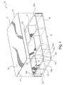
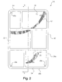
- an exemplary EMI shield in accordance with the present invention is shown generally at 10 in the several views of Figs. 1-3 as having one or more compartments, one of which is referenced at 11, for enclosing circuitry of an electronic device.
- shield 10 includes a first member or section, 12, and a mating second member or section, 14, which is joined to the first section 12, and which is configured to partition the shield 10 into the one or more compartments 11.
- Each of the compartments 11 may be used to house separate components, circuits, or areas of the circuitry of the device for the purpose of electromagnetically isolating the same from other such components, circuits, or areas of the circuitry.
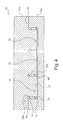
- first section 12 may be generally planar, and in the illustrative embodiment of Figs. 1-3 has an outer surface, 20, and an inner surface, 22.
- First section 12 may be stamped, die cut, or otherwise formed into a variety of shapes, which shape may be defined by an outer margin, 24, and otherwise may be provided as a thin metal sheet having a z-axis thickness, referenced at t 1 in the cross-sectional view of Fig. 3 , of, for example, not greater than about 10 mils (0.25 mm), and, typically, between about 3-5 mils (0.075-0.125 mm) or less.
- a z-axis thickness referenced at t 1 in the cross-sectional view of Fig. 3 , of, for example, not greater than about 10 mils (0.25 mm), and, typically, between about 3-5 mils (0.075-0.125 mm) or less.
- the section alternatively may be contoured or otherwise non-planar as the application may require.
- the first section 12 may be formed of a sheet of an aluminum or aluminum alloy material.
- a sheet of another metal such as zinc, magnesium, or steel, or a combination or alloy thereof, may be substituted or used in combination with the aluminum or aluminum alloy material.
- the second section 14 is joined to the first member, and has one or more walls, a grouping of adjacent ones of which is referenced at 30a-d, which extend, either generally perpendicularly as shown or, alternatively, at an angle, from the inner surface 22 of the first section 12. As is shown for the walls 30a-d, each such grouping of adjacent walls 30, together with the surface 22 of the first member 12 may define a separate one of the compartments 11. It is to be understood that, as used herein, the term "wall” may refer to an exterior wall or portion thereof, such as is referenced at 30a and 30b, and/or to an interior wall or portion thereof, such as either of walls 30c or 30d.
- the walls 30 each may have a z-axis thickness, referenced at t 2 in the cross-sectional view of Fig. 3 , which may be the same or different, and which otherwise may be between about 3-10 mils (0.075-0.254 mm).
- each of the walls 30 extends intermediate a first end surface, referenced at 32 for the wall 30b, adjacent the first section inner surface 22, and a distal second end surface, referenced at 34 for wall 30b.
- the first end surfaces 32 which, as is shown may be generally coterminous such that the interface, referenced at 36, which is defined collectively thereby is generally planar. Alternatively, such as may depend upon the contouring of the first section 12, the first end surfaces may terminate non-planarly.
- the second end surfaces 34 may terminate to define an interface, 38, which is generally planar as shown or, instead, is non-planar.
- the second end surface which may be used, for example, to contact the ground trace of a PCB, may be generally flat as shown or, alternatively, rounded, notched, flanged, tapered, or otherwise shaped.
- the second section 14 further may be formed as having features, such as the corner throughholes referenced at 40a-d, for the attachment using screws or other fasteners of the shield to a PCB or other part of the device.
- the throughholes 40 may be otherwise configured such as for pins or for heat-stalced threaded metal or other inserts.
- the second section 14 may be formed as having features for a snap or other interference fit or mechanical engagement with another part of the device.
- a flange also may be provided as extending outwardly from the end surfaces 34 about the entirety or a portion of the outer perimeter, referenced at 42, of the shield 10 which is defined by the exterior walls thereof.
- the second section 14 may be molded or otherwise formed in one or more pieces of an electrically-conductively composite material. which may be the same or different in each piece. Such material may be formulated, as may be more fully described in U.S. Pat. Nos.
- the polymeric component which itself may be a blend or other admixture, may be a thermoplastic or thermoset, and specifically may be selected as depending upon one or more of operating temperature, hardness, chemical compatibility, resiliency, compliancy, compression-deflection, compression set, flexibility, ability to recover after deformation, modulus, tensile strength, elongation, force defection, flammability, or other chemical or physical property.
- suitable materials may include, particularly, polyurethanes, silicones, fluorosilicones, polycarbonates, ethylene vinyl acetates (EVA), acrylonitrile-butadiene-styrenes (ABS), polysulfones, acrylics, polyvinyl chlorides (FVC), polyphenylene ethers, polystyrenes, polyamides, nylons, polyolefins, poly(ether ether ketones), polyimides, polyetherimides, polybutylene terephthalates, polyethylene terephthalates, fluoropolymers, polyesters, acetals, liquid crystal polymers, polymethylacrylates, polyphenylene oxides, polystyrenes, epoxies, phenolics, chlorosulfonates, polybutadienes, buna-N, butyls, neoprenes, nitriles, polyisoprenes, natural rubbers, and copolymer rubbers such as
- the polymeric component generally may form a binder or other continuous or matrix phase within the material into which the electrically-conductive particulate filler may be dispersed as a discrete phase.
- the filler generally is included within the binder in a proportion sufficient to provide the level of electrical conductivity which is desired for the intended application. For most applications, a bulk or volume resistivity of not greater than about 1,000 ⁇ -cm, and/or a surface resistance of not greater than about 1000 ⁇ /sq., would be considered acceptable, and would translate to a filler loading which generally may be between about 5-95% by weight, based on the total volume or weight, as the case may be, of the compound.
- the filler may be of any shape, or combination of shapes, and is referred broadly herein as being "particulate,” which should be understood to include solid or hollow spheres and microspheres, elastomeric balloons, flakes, platelets, fibers, rods, irregularly-shaped particles, fibers, which may be chopped or milled or whiskers, and powders.
- particle size or distribution of the filler which may be a diameter, imputed diameter, length, or other dimension of the particulate typically will range from about 0.01 mil (0.25 ⁇ m) to about 10 mils (250 ⁇ m) for powders, and from about 0.004 inch (0.1 mm) to about 1 inch (25 mm) for fibers.
- Suitable electrically-conductive fillers include: nonmetals such as carbon, graphite, and inherently, i.e., intrinsically, conductive polymers; noble and non-noble metals such as gold, silver, nickel, copper, tin, aluminum, and nickel; noble or non-noble metal-plated, clad, metallized, or otherwise coated noble and non-noble metals such as gold or silver-plated copper, nickel, or aluminum, and tin or nickel-plated copper, silver, bismuth, indium, and lead; noble or non-noble metal coated non-metals such as gold, silver and/or nickel-plated or clad graphite, i.e., gold plated nickel clad graphite, glass, ceramics, plastics, elastomers, and mica; non-metal coated metal and non-metals; and combinations and mixtures thereof.
- nonmetals such as carbon, graphite, and inherently, i.e., intrinsically, conductive polymers
- the electrically-conductive filler specifically may be selected as depending upon one or more of conductivity, resin demand, hardness, chemical compatibility, such as with the polymeric component, and cost.
- the coating may be formed of one or more layers of the same material, or of layers of different materials.
- fillers and additives may be included in the formulation of the material depending upon the requirements of the particular application envisioned.
- Such fillers and additives may include wetting agents or surfactants, pigments, dispersants, dyes, and other colorants, opacifying agents, foaming or anti-foaming agents, anti-static agents, coupling agents such as titanates, chain extending oils, tackifiers, flow modifiers, pigments, lubricants such as molybdenum disulfide (MoS 2 ), silanes, peroxides, film-reinforcing polymers and other agents, stabilizers, emulsifiers, antioxidants, thickeners, and/or flame retardants and other fillers such as aluminum trihydrate, antimony trioxide, metal oxides and salts, intercalated graphite particles, phosphate esters, decabromodiphenyl oxide, borates, phosphates, halogenated compounds, glass, silica, which may be fu
- the formulation for the electrically-conductively composite material of the second section 14 may be compounded in a conventional mixing apparatus as an admixture of the polymer and filler components, and any additional fillers or additives. Alternatively, and as may be further described in U.S. Patent Nos.
- the material may be provided in the form of pellets having a core of nickel-coated carbon or graphite fibers, or other conductive fibers, which are wire-die or otherwise coated or encased within an outer coating of the polymer component which may be a thermoplastic. Such pellets may be injection molded to form the second section 14.
- the above-described pellets, or other compound of the electrically-conductively composite material may be used in an insert molding process to both form the second section 14 and to join the section to the first section 12.
- Such process is schematically illustrated at 50 in the view of Fig. 4 .
- the stamping or other form of the first section 12 may be positioned into a cavity, 52, defined between or formed into one of a pair of mold halves, 54a-b, with the remainder of the cavity 52 defining the configuration of the second section 14. With the mold halves 54 closed, such as along the parting line which is shown at 56, the compound of the composite material may be introduced under pressure or otherwise into the remainder of the cavity.
- the mold halves 54 may be opened and the finished or substantially finished shield 10 thereby formed may be released therefrom.
- the second section 14 of the shield 10 may be molded and bonded or otherwise joined to the first section 12 in a single operation.
- the second section may be joined to the first section 12 along the interface 36.
- the respective sections 12 and 14 may be constructed as separated parts which are mechanically fastened or interferingly or otherwise engaged, or adhesively bonded or otherwise joined, the sections 12 and 14 are shown in the illustrative embodiment to be self-adherent or bonded.
- Such bonding may be via mechanical forces, fusion or chemical bonding, and/or electrostatic, van der Waals, or other valance or attractive forces, as may depend upon the composition and the compatibility of the metal and plastic materials forming the sections 12 and 14.
- the metal sheet of the first section 12 may be stamped, cut, or otherwise formed as having one or more apertures, one of which is referenced in phantom at 60 in Figs. 3 and 4 , for the flow therethrough of the composite material of the second section 14.
- the metal sheet of the first section 12 also may be fabricated as having fingers, flanges, or other features into or around which the material of the second section 14 may flow.
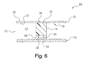
- the assembly 70 is shown to include a PCB, 72, which may be a component or module of an electronic device.
- various electronic components one of which is referenced at 74, or other circuitry may be mounted on the PCB 72, and may be grouped into different circuits, one of which is referenced at 76, such as may be delineated by the pattern of a ground trace, referenced in phantom at 78.
- the shield 10 may be attached or otherwise joined to the PCB 72 by means, for example, of the screws 80 received through the holes 82 of the PCB and into the throughholes 40 of the second section 14.
- the shield 10 may be attached or otherwise joined to the PCB 72 by other mechanical means, such as a clip, or by means of bonding with a metal solder or with an adhesive which may be electrically-conductive, or a double-sided tape.
- the interface 38 As joined to the PCB 72, the interface 38, or a portion thereof, may be in alignment and electrical contact with the ground trace 78 to thereby isolate one or more, or each, of the circuits 76 from the other circuits 76 or from other components within the device, or from other devices.
- electrical contact between the interface 38 and the ground trace 78 or other part of the device may be enhanced by means of a separate layer, 92, of an electrically-conductive material interposed between the interface and the trace.
- such layer 82 may be provided to extend continuously or discontinuously between all or a portion of the interfacing surfaces 38 and 78, and additionally may provide an environmental seal therebetween.
- the layer 92 may be the solder or adhesive which may be used to bond the shield 10 to the PCB 72, or the layer may be an other coating such as a metal or a metal-filled paint which may be applied to one or both of the interfacing surfaces 38 and 78 such as by flame or arc-wire spraying, dipping, painting, screen or transfer printing, dispensing, extrusion, cladding, metallizing, laminating, electroless or electrolytic plating, vacuum or chemical vapor deposition, evaporation, sputterring, plasma coating, or the like.
- the layer may be electrically-conductive gasket or gasket-like material.
- such material may be provided in the form of a gasket having a resilient core element affording gap-filling capabilities, which core element may be loaded, sheathed, or coated with an electrically conductive element.
- the resilient core element which may be foamed or unfoamed, solid or tubular, typically may be molded, extruded, die-cut, or otherwise formed of an elastomeric thermoplastic material such as a polyolefm, polyvinyl chloride, or a polypropylene-EPDM blend, or a thermoplastic or thermosetting rubber such as a butadiene, styrene-butadiene, nitrile, chlorosulfonate, neoprene, urethane, silicone, or fluorosilicone.
- an elastomeric thermoplastic material such as a polyolefm, polyvinyl chloride, or a polypropylene-EPDM blend
- a thermoplastic or thermosetting rubber such as a butadiene, styrene-butadiene, nitrile, chlorosulfonate, neoprene, urethane, silicone, or fluorosilicone.
- Conductive materials for the filler, sheathing, or coating include metal or metal-plated particles, fabrics, meshes, and fibers.
- Preferred metals include copper, nickel, silver, aluminum, tin or an alloy such as Monel, with preferred fibers and fabrics including natural or synthetic fibers such as cotton, wool, silk, cellulose, polyester, polyamide, nylon, polyimide.
- Other conductive particles and fibers such as carbon, graphite, plated glass, or a conductive polymer material may be substituted.
- the gasket alternatively, may be provided to be of an all-metal, knitted wire construction, or as a over-molded or formed-in-place (FIP) bead of a curable, electrically-conductive silicone or urethane composition.
- FIP over-molded or formed-in-place
- the composition may be dispensed in a fluent state onto one or the other of the surfaces 38 and 78, and then cured or foamed in situ via the application of heat or with atmospheric moisture, UV,
- Means of securing the gasket or gasket material to one or the other of the surfaces 38 and 78 include pressure-sensitive adhesive tapes or other layers (not shown), which may be filled to be electrically conductive, interposed between the surface and the gasket. Alternatively, mechanical means of attachment such as clips, fasteners, or a tough-in-groove or other interference fit may be employed. In the case of an over-molded or FIP construction, the gasket may be self-bonded by chemical, mechanical, or other adhesive forces to the surface. EMI shielding gaskets and their methods of manufacture and use are further described in U.S. Patent Nos.
Landscapes
- Engineering & Computer Science (AREA)
- Microelectronics & Electronic Packaging (AREA)
- Shielding Devices Or Components To Electric Or Magnetic Fields (AREA)
Claims (38)
- Elektromagnetische Störbeeinflussungsabschirmung (10) mit mindestens einer Kammer (11), die auf oder über einer gedruckten Schaltkreisplatine (72) befestigbar ist zum Einschließen eines Schaltkreises (74, 76) einer elektronischen Vorrichtung, wobei die Abschirmung aufweist:ein aus einem dünnen Metallblech gebildetes erstes Element (12) undein aus einem elektrisch leitfähigen Verbundmaterial mit einer Mischung aus einer polymeren Komponente und einer elektrisch leitfähigen partikelförmigen Füllstoffkomponente gebildetes zweites Element (14), wobei das zweite Element mit dem ersten Element verbunden ist, so dass eine einstückige Abschirmung gebildet wird, und das zweite Element mindestens eine Wand (30a-d) aufweist, die sich von dem ersten Element aus erstreckt und die zusammen mit dem ersten Element mindestens einen Abschnitt der Kammer bildet.
- Abschirmung nach Anspruch 1, wobei die polymere Komponente ein oder mehrere thermohärtende oder thermoplastische Polymere oder Copolymere oder eine Mischung davon aufweist.
- Abschirmung nach Anspruch 1, wobei die polymere Komponente aus der Gruppe ausgewählt ist, die gebildet wird aus Epoxidhharzen, Phenolharzen, Po-ly(etheretherketonen), Polyimiden, Polyolefinen, Polyetherimiden, Polybutylenterephthalaten, Polyethylenterephthalaten, Nylon, Polyamiden, Fluorpolymeren, Polysulfonen, Polyestern, Acetalhomo- und -copolymeren, Flüssigkristallpolymeren, Polyacrylen, Polymethylacrylaten, Poly(ester- und -ether-Urethanen), Polyurethanen, Acrylnitril-Butadien-Styrol, Polyvinylchloriden und Polyphenylenethern, Polyphenylenoxiden, Polystyrolen, Polycarbonaten und Copolymeren und Mischungen davon.
- Abschirmung nach Anspruch 1, wobei die Abschirmung eine elektromagnetische Störbeeinflussungsabschirmungseffektivität von mindestens ungefähr 60 dB im Wesentlichen über einen Frequenzbereich zwischen ungefähr 10 MHz und ungefähr 10 GHz aufweist.
- Abschirmung nach Anspruch 1, wobei das Verbundmaterial einen Volumenwiderstand von nicht größer als ungefähr 1.000 Ω-cm aufweist.
- Abschirmung nach Anspruch 1, wobei das Verbundmaterial zwischen ungefähr 5-95 Gew.-% der Füllmaterialkomponente aufweist.
- Abschirmung nach Anspruch 1, wobei das Metallblech eine Dicke von nicht größer als ungefähr 10 mil (0,125 mm) aufweist.
- Abschirmung nach Anspruch 1, wobei die Wand des zweiten Elements eine Dicke zwischen ungefähr 3 mil und 10 mil (0,075-0,254 mm) aufweist.
- Abschirmung nach Anspruch 1, wobei das zweite Element auf das erste Element selbstgebondet ist.
- Abschirmung nach Anspruch 1, wobei das Blech aus Aluminium, Zink, Magnesium, Stahl oder einer Kombination oder einer Legierung davon gebildet ist.
- Abschirmung nach Anspruch 1, wobei sich die Wand von dem ersten Element zu einer Endfläche erstreckt, wobei die Endfläche auf einem Teil der Vorrichtung anordenbar ist.
- Abschirmung nach Anspruch 11, darüber hinaus mit einer auf der Endfläche angeordneten elektrisch leitfähigen Schicht oder Dichtung.
- Abschirmung nach Anspruch 12, wobei die elektrisch leitfähige Schicht ein Metall oder ein mit elektrisch leitfähigen Teilchen gefülltes Harz aufweist.
- Abschirmung nach Anspruch 12, wobei die Dichtung ein mit elektrisch leitfähigen Teilchen gefülltes elastomeres Harz aufweist.
- Abschirmung nach Anspruch 12, wobei die Dichtung oder die Schicht auf der Endfläche selbstklebend ist.
- Abschirmung nach Anspruch 1, wobei die elektrisch leitfähige teilchenförmige Füllstoffkomponente elektrisch leitende Fasern aufweist.
- Abschirmung nach Anspruch 16, wobei die elektrisch leitfähigen Fasern ausgewählt sind aus der Gruppe, die gebildet aus: Graphit, Karbon, inhärent leitfähigem Polymer und Metallfasern, metallischen oder nichtmetallischen Fasern mit einer elektrisch leitenden Beschichtung und Mischungen und Kombinationen davon.
- Abschirmung nach Anspruch 17, wobei die elektrisch leitende Beschichtung eine oder mehrere Schichten aus Karbon, Graphit oder einem oder mehreren inhärent leitenden Polymeren oder Metallen oder einer Kombination davon aufweist.
- Abschirmung nach Anspruch 16, wobei die Fasern eine durchschnittliche Länge zwischen ungefähr 0,004 und 1 Inch (0,1-25 mm) aufweisen.
- Abschirmung nach Anspruch 1, wobei die Kammer über dem Schaltkreis der Vorrichtung aufgenommen ist.
- Anordnung nach Anspruch 20, wobei die polymere Komponente eines oder mehrere thermohärtende oder thermoplastische Polymere oder Copolymere oder eine Mischung davon aufweist.
- Anordnung nach Anspruch 20, wobei die polymere Komponente ausgewählt ist aus der Gruppe, die gebildet ist aus Epoxidharzen, Phenolharzen, Poly(etheretherketonen), Polyimiden, Polyolefinen, Polyetherimiden, Polybutylenterephthalaten, Polyethylenterephthalaten, Nylon, Polyamiden, Fluoropolymeren, Polysulfonen, Polyestern, Acetalhomo- und - copolymeren, Flüssigkristallpolymeren, Polyacrylen, Polymethylacrylaten, Poly(ester- und -ether-Urethanen), Polyurethanen, Acrylnitril-Butadien-Styrol, Polyvinylchloriden, Polyphenylenethern, Polyphenylenoxiden, Polystyrolen, Polycarbonaten und Copolymeren und Mischungen davon.
- Anordnung nach Anspruch 20, wobei die Abschirmung eine elektromagnetische Störbeeinflussungsabschirmungseffektivität von mindestens ungefähr 60 dB im Wesentlichen über einen Frequenzbereich zwischen ungefähr 10 MHz und ungefähr 10 GHz aufweist.
- Anordnung nach Anspruch 20, wobei das Verbundmaterial einen Volumenwiderstand aufweist, der nicht größer ist als ungefähr 1.000 Ω-cm.
- Anordnung nach Anspruch 20, wobei das Verbundmaterial zwischen ungefähr 5 und 95 Gew.-% der Füllstoffkomponente aufweist.
- Anordnung nach Anspruch 20, wobei das Metallblech eine Dicke nicht größer als ungefähr 10 mil (0,125 mm) aufweist.
- Anordnung nach Anspruch 20, wobei die Wand des zweiten Elements eine Dicke zwischen ungefähr 3 und 10 Inch (0,075-0,254 mm) aufweist.
- Anordnung nach Anspruch 20, wobei das zweite Element auf das erste Element selbstgebondet ist.
- Anordnung nach Anspruch 20, wobei das Blech aus Aluminium, Zink, Magnesium, Stahl oder einer Kombination oder einer Legierung davon gebildet ist.
- Anordnung nach Anspruch 20, wobei sich die Wand von dem ersten Element aus zu einer Endfläche erstreckt, wobei die Endfläche auf einem Teil der Vorrichtung, die zusammen mit der Kammer den Schaltkreis umschließt, angeordnet ist.
- Anordnung nach Anspruch 30 darüber hinaus mit einer elektrisch leitenden Schicht oder Dichtung, die zwischen der Endfläche und dem Vorrichtungsteil angeordnet ist.
- Anordnung nach Anspruch 31, wobei die elektrisch leitende Schicht ein Metall oder ein mit elektrisch leitenden Teilchen gefülltes Harz aufweist.
- Anordnung nach Anspruch 31, wobei die Dichtung ein mit elektrisch leitenden Teilchen gefülltes elastomeres Harz aufweist.
- Anordnung nach Anspruch 31, wobei die Dichtung oder Schicht auf der Endfläche selbstklebend ist.
- Anordnung nach Anspruch 20, wobei die elektrisch leitende teilchenförmige Füllstoffkomponente elektrisch leitende Fasern aufweist.
- Anordnung nach Anspruch 35, wobei die elektrisch leitenden Fasern ausgewählt sind aus der Gruppe, die besteht aus: Graphit, Karbon, inhärent leitenden Polymer- und Metallfasern, metallischen oder nichtmetallischen Fasern mit einer elektrisch leitenden Beschichtung und Mischungen und Kombinationen davon.
- Anordnung nach Anspruch 36, wobei die elektrisch leitende Beschichtung eine oder mehrere Schichten aus Karbon, Graphit oder einem oder mehreren inhärent leitenden Polymeren oder Metallen oder einer Kombination davon aufweist.
- Anordnung nach Anspruch 35, wobei die Fasern eine durchschnittliche Länge von zwischen ungefähr 0,004 und ungefähr 1 Inch (0,1-25 mm) aufweisen.
Applications Claiming Priority (5)
| Application Number | Priority Date | Filing Date | Title |
|---|---|---|---|
| US44726303P | 2003-02-13 | 2003-02-13 | |
| US447263P | 2003-02-13 | ||
| US46925003P | 2003-05-09 | 2003-05-09 | |
| US469250P | 2003-05-09 | ||
| PCT/US2004/001936 WO2004075616A1 (en) | 2003-02-13 | 2004-01-26 | Combination metal and plastic emi shield |
Publications (2)
| Publication Number | Publication Date |
|---|---|
| EP1593293A1 EP1593293A1 (de) | 2005-11-09 |
| EP1593293B1 true EP1593293B1 (de) | 2011-07-06 |
Family
ID=32912255
Family Applications (1)
| Application Number | Title | Priority Date | Filing Date |
|---|---|---|---|
| EP04705236A Expired - Lifetime EP1593293B1 (de) | 2003-02-13 | 2004-01-26 | Kombinierte metall- und kunststoff-emi-abschirmung |
Country Status (3)
| Country | Link |
|---|---|
| EP (1) | EP1593293B1 (de) |
| AT (1) | ATE515934T1 (de) |
| WO (1) | WO2004075616A1 (de) |
Families Citing this family (4)
| Publication number | Priority date | Publication date | Assignee | Title |
|---|---|---|---|---|
| JP2009532574A (ja) * | 2006-04-05 | 2009-09-10 | サビック・イノベーティブ・プラスチックス・アイピー・ベスローテン・フェンノートシャップ | ポリ(アリーレンエーテル)/ポリアミド組成物、方法、及び物品 |
| EP2929767A4 (de) * | 2012-10-19 | 2017-12-06 | Tongyu Technology Oy | Funkfrequenzfilteranordnung |
| KR20170123747A (ko) * | 2016-04-29 | 2017-11-09 | 삼성전자주식회사 | 차폐 부재 및 그를 포함하는 전자 장치 |
| CN111587057A (zh) * | 2020-05-15 | 2020-08-25 | 深圳市飞荣达科技股份有限公司 | 屏蔽盒 |
Family Cites Families (4)
| Publication number | Priority date | Publication date | Assignee | Title |
|---|---|---|---|---|
| US5660380A (en) * | 1995-08-15 | 1997-08-26 | W. L. Gore & Associates, Inc. | Vacuum fixture and method for dimensioning and manipulating materials |
| SE511926C2 (sv) * | 1997-04-16 | 1999-12-20 | Ericsson Telefon Ab L M | Skärmningshölje jämte förfarande för framställning och användning av ett skärmningshölje samt mobiltelefon med skärmningshölje |
| JPH10322076A (ja) * | 1997-05-23 | 1998-12-04 | Nec Eng Ltd | 高周波用シールドケース構造 |
| AU2002230453A1 (en) * | 2000-11-20 | 2002-06-03 | Owens Corning | Interference mitigation through conductive thermoplastic composite materials |
-
2004
- 2004-01-26 EP EP04705236A patent/EP1593293B1/de not_active Expired - Lifetime
- 2004-01-26 WO PCT/US2004/001936 patent/WO2004075616A1/en not_active Ceased
- 2004-01-26 AT AT04705236T patent/ATE515934T1/de not_active IP Right Cessation
Also Published As
| Publication number | Publication date |
|---|---|
| EP1593293A1 (de) | 2005-11-09 |
| WO2004075616A1 (en) | 2004-09-02 |
| ATE515934T1 (de) | 2011-07-15 |
Similar Documents
| Publication | Publication Date | Title |
|---|---|---|
| US7326862B2 (en) | Combination metal and plastic EMI shield | |
| US7005573B2 (en) | Composite EMI shield | |
| US6784363B2 (en) | EMI shielding gasket construction | |
| EP2338319B1 (de) | Emi-abschirmung aus elektrisch leitendem schaumstoff | |
| CN2865209Y (zh) | 具有热喷涂金属保形涂层的电子装置 | |
| US7446265B2 (en) | Board level shielding module | |
| CN1274192C (zh) | 用于低闭合力电磁干扰的屏蔽应用的复合波形垫片 | |
| EP2291446B1 (de) | Funkentstörmaterialien | |
| US20030015334A1 (en) | Electronics enclosure having an interior EMI shielding and cosmetic coating | |
| EP1386527A1 (de) | Herstellung eines gehäuses für elektronik mit einer metallisierten schutzschicht | |
| US20030091777A1 (en) | Clean release tape for EMI shielding | |
| US20120181080A1 (en) | Combination glass/ceramic particles for emi shielding | |
| EP1593293B1 (de) | Kombinierte metall- und kunststoff-emi-abschirmung | |
| EP4013203B1 (de) | Elektrisch und thermisch leitende dichtungen | |
| ES2367631T3 (es) | Pantalla emi de metal y de plástico en combinación. | |
| CN114628055A (zh) | 导电导热垫圈、制造导电导热垫圈的方法、电装置 |
Legal Events
| Date | Code | Title | Description |
|---|---|---|---|
| PUAI | Public reference made under article 153(3) epc to a published international application that has entered the european phase |
Free format text: ORIGINAL CODE: 0009012 |
|
| 17P | Request for examination filed |
Effective date: 20050728 |
|
| AK | Designated contracting states |
Kind code of ref document: A1 Designated state(s): AT BE BG CH CY CZ DE DK EE ES FI FR GB GR HU IE IT LI LU MC NL PT RO SE SI SK TR |
|
| AX | Request for extension of the european patent |
Extension state: AL LT LV MK |
|
| DAX | Request for extension of the european patent (deleted) | ||
| 17Q | First examination report despatched |
Effective date: 20100629 |
|
| GRAP | Despatch of communication of intention to grant a patent |
Free format text: ORIGINAL CODE: EPIDOSNIGR1 |
|
| GRAS | Grant fee paid |
Free format text: ORIGINAL CODE: EPIDOSNIGR3 |
|
| GRAA | (expected) grant |
Free format text: ORIGINAL CODE: 0009210 |
|
| AK | Designated contracting states |
Kind code of ref document: B1 Designated state(s): AT BE BG CH CY CZ DE DK EE ES FI FR GB GR HU IE IT LI LU MC NL PT RO SE SI SK TR |
|
| REG | Reference to a national code |
Ref country code: GB Ref legal event code: FG4D |
|
| REG | Reference to a national code |
Ref country code: CH Ref legal event code: EP |
|
| REG | Reference to a national code |
Ref country code: IE Ref legal event code: FG4D |
|
| REG | Reference to a national code |
Ref country code: DE Ref legal event code: R096 Ref document number: 602004033360 Country of ref document: DE Effective date: 20110901 |
|
| REG | Reference to a national code |
Ref country code: NL Ref legal event code: VDEP Effective date: 20110706 |
|
| REG | Reference to a national code |
Ref country code: ES Ref legal event code: FG2A Ref document number: 2367631 Country of ref document: ES Kind code of ref document: T3 Effective date: 20111107 |
|
| PG25 | Lapsed in a contracting state [announced via postgrant information from national office to epo] |
Ref country code: SI Free format text: LAPSE BECAUSE OF FAILURE TO SUBMIT A TRANSLATION OF THE DESCRIPTION OR TO PAY THE FEE WITHIN THE PRESCRIBED TIME-LIMIT Effective date: 20110706 |
|
| REG | Reference to a national code |
Ref country code: AT Ref legal event code: MK05 Ref document number: 515934 Country of ref document: AT Kind code of ref document: T Effective date: 20110706 |
|
| PG25 | Lapsed in a contracting state [announced via postgrant information from national office to epo] |
Ref country code: FI Free format text: LAPSE BECAUSE OF FAILURE TO SUBMIT A TRANSLATION OF THE DESCRIPTION OR TO PAY THE FEE WITHIN THE PRESCRIBED TIME-LIMIT Effective date: 20110706 Ref country code: NL Free format text: LAPSE BECAUSE OF FAILURE TO SUBMIT A TRANSLATION OF THE DESCRIPTION OR TO PAY THE FEE WITHIN THE PRESCRIBED TIME-LIMIT Effective date: 20110706 Ref country code: BE Free format text: LAPSE BECAUSE OF FAILURE TO SUBMIT A TRANSLATION OF THE DESCRIPTION OR TO PAY THE FEE WITHIN THE PRESCRIBED TIME-LIMIT Effective date: 20110706 Ref country code: PT Free format text: LAPSE BECAUSE OF FAILURE TO SUBMIT A TRANSLATION OF THE DESCRIPTION OR TO PAY THE FEE WITHIN THE PRESCRIBED TIME-LIMIT Effective date: 20111107 Ref country code: SE Free format text: LAPSE BECAUSE OF FAILURE TO SUBMIT A TRANSLATION OF THE DESCRIPTION OR TO PAY THE FEE WITHIN THE PRESCRIBED TIME-LIMIT Effective date: 20110706 |
|
| PG25 | Lapsed in a contracting state [announced via postgrant information from national office to epo] |
Ref country code: GR Free format text: LAPSE BECAUSE OF FAILURE TO SUBMIT A TRANSLATION OF THE DESCRIPTION OR TO PAY THE FEE WITHIN THE PRESCRIBED TIME-LIMIT Effective date: 20111007 Ref country code: CY Free format text: LAPSE BECAUSE OF FAILURE TO SUBMIT A TRANSLATION OF THE DESCRIPTION OR TO PAY THE FEE WITHIN THE PRESCRIBED TIME-LIMIT Effective date: 20110706 Ref country code: AT Free format text: LAPSE BECAUSE OF FAILURE TO SUBMIT A TRANSLATION OF THE DESCRIPTION OR TO PAY THE FEE WITHIN THE PRESCRIBED TIME-LIMIT Effective date: 20110706 |
|
| PG25 | Lapsed in a contracting state [announced via postgrant information from national office to epo] |
Ref country code: SK Free format text: LAPSE BECAUSE OF FAILURE TO SUBMIT A TRANSLATION OF THE DESCRIPTION OR TO PAY THE FEE WITHIN THE PRESCRIBED TIME-LIMIT Effective date: 20110706 Ref country code: CZ Free format text: LAPSE BECAUSE OF FAILURE TO SUBMIT A TRANSLATION OF THE DESCRIPTION OR TO PAY THE FEE WITHIN THE PRESCRIBED TIME-LIMIT Effective date: 20110706 |
|
| PLBE | No opposition filed within time limit |
Free format text: ORIGINAL CODE: 0009261 |
|
| STAA | Information on the status of an ep patent application or granted ep patent |
Free format text: STATUS: NO OPPOSITION FILED WITHIN TIME LIMIT |
|
| PG25 | Lapsed in a contracting state [announced via postgrant information from national office to epo] |
Ref country code: EE Free format text: LAPSE BECAUSE OF FAILURE TO SUBMIT A TRANSLATION OF THE DESCRIPTION OR TO PAY THE FEE WITHIN THE PRESCRIBED TIME-LIMIT Effective date: 20110706 Ref country code: RO Free format text: LAPSE BECAUSE OF FAILURE TO SUBMIT A TRANSLATION OF THE DESCRIPTION OR TO PAY THE FEE WITHIN THE PRESCRIBED TIME-LIMIT Effective date: 20110706 |
|
| 26N | No opposition filed |
Effective date: 20120411 |
|
| PG25 | Lapsed in a contracting state [announced via postgrant information from national office to epo] |
Ref country code: DK Free format text: LAPSE BECAUSE OF FAILURE TO SUBMIT A TRANSLATION OF THE DESCRIPTION OR TO PAY THE FEE WITHIN THE PRESCRIBED TIME-LIMIT Effective date: 20110706 |
|
| REG | Reference to a national code |
Ref country code: DE Ref legal event code: R097 Ref document number: 602004033360 Country of ref document: DE Effective date: 20120411 |
|
| PG25 | Lapsed in a contracting state [announced via postgrant information from national office to epo] |
Ref country code: MC Free format text: LAPSE BECAUSE OF NON-PAYMENT OF DUE FEES Effective date: 20120131 |
|
| REG | Reference to a national code |
Ref country code: CH Ref legal event code: PL |
|
| REG | Reference to a national code |
Ref country code: IE Ref legal event code: MM4A |
|
| PG25 | Lapsed in a contracting state [announced via postgrant information from national office to epo] |
Ref country code: LI Free format text: LAPSE BECAUSE OF NON-PAYMENT OF DUE FEES Effective date: 20120131 Ref country code: CH Free format text: LAPSE BECAUSE OF NON-PAYMENT OF DUE FEES Effective date: 20120131 |
|
| PG25 | Lapsed in a contracting state [announced via postgrant information from national office to epo] |
Ref country code: IE Free format text: LAPSE BECAUSE OF NON-PAYMENT OF DUE FEES Effective date: 20120126 |
|
| PG25 | Lapsed in a contracting state [announced via postgrant information from national office to epo] |
Ref country code: BG Free format text: LAPSE BECAUSE OF FAILURE TO SUBMIT A TRANSLATION OF THE DESCRIPTION OR TO PAY THE FEE WITHIN THE PRESCRIBED TIME-LIMIT Effective date: 20111006 |
|
| PG25 | Lapsed in a contracting state [announced via postgrant information from national office to epo] |
Ref country code: TR Free format text: LAPSE BECAUSE OF FAILURE TO SUBMIT A TRANSLATION OF THE DESCRIPTION OR TO PAY THE FEE WITHIN THE PRESCRIBED TIME-LIMIT Effective date: 20110706 |
|
| PG25 | Lapsed in a contracting state [announced via postgrant information from national office to epo] |
Ref country code: LU Free format text: LAPSE BECAUSE OF NON-PAYMENT OF DUE FEES Effective date: 20120126 |
|
| PG25 | Lapsed in a contracting state [announced via postgrant information from national office to epo] |
Ref country code: HU Free format text: LAPSE BECAUSE OF FAILURE TO SUBMIT A TRANSLATION OF THE DESCRIPTION OR TO PAY THE FEE WITHIN THE PRESCRIBED TIME-LIMIT Effective date: 20040126 |
|
| REG | Reference to a national code |
Ref country code: FR Ref legal event code: PLFP Year of fee payment: 12 |
|
| REG | Reference to a national code |
Ref country code: FR Ref legal event code: PLFP Year of fee payment: 13 |
|
| REG | Reference to a national code |
Ref country code: FR Ref legal event code: PLFP Year of fee payment: 14 |
|
| REG | Reference to a national code |
Ref country code: FR Ref legal event code: PLFP Year of fee payment: 15 |
|
| PGFP | Annual fee paid to national office [announced via postgrant information from national office to epo] |
Ref country code: ES Payment date: 20180201 Year of fee payment: 15 Ref country code: DE Payment date: 20180129 Year of fee payment: 15 Ref country code: GB Payment date: 20180129 Year of fee payment: 15 |
|
| PGFP | Annual fee paid to national office [announced via postgrant information from national office to epo] |
Ref country code: IT Payment date: 20180122 Year of fee payment: 15 Ref country code: FR Payment date: 20180125 Year of fee payment: 15 |
|
| REG | Reference to a national code |
Ref country code: DE Ref legal event code: R119 Ref document number: 602004033360 Country of ref document: DE |
|
| GBPC | Gb: european patent ceased through non-payment of renewal fee |
Effective date: 20190126 |
|
| PG25 | Lapsed in a contracting state [announced via postgrant information from national office to epo] |
Ref country code: DE Free format text: LAPSE BECAUSE OF NON-PAYMENT OF DUE FEES Effective date: 20190801 Ref country code: FR Free format text: LAPSE BECAUSE OF NON-PAYMENT OF DUE FEES Effective date: 20190131 |
|
| PG25 | Lapsed in a contracting state [announced via postgrant information from national office to epo] |
Ref country code: GB Free format text: LAPSE BECAUSE OF NON-PAYMENT OF DUE FEES Effective date: 20190126 |
|
| PG25 | Lapsed in a contracting state [announced via postgrant information from national office to epo] |
Ref country code: IT Free format text: LAPSE BECAUSE OF NON-PAYMENT OF DUE FEES Effective date: 20190126 |
|
| REG | Reference to a national code |
Ref country code: ES Ref legal event code: FD2A Effective date: 20200310 |
|
| PG25 | Lapsed in a contracting state [announced via postgrant information from national office to epo] |
Ref country code: ES Free format text: LAPSE BECAUSE OF NON-PAYMENT OF DUE FEES Effective date: 20190127 |
|
| P01 | Opt-out of the competence of the unified patent court (upc) registered |
Effective date: 20230524 |