EP1593186B1 - Stosstoleranter verbinder - Google Patents
Stosstoleranter verbinder Download PDFInfo
- Publication number
- EP1593186B1 EP1593186B1 EP03780484A EP03780484A EP1593186B1 EP 1593186 B1 EP1593186 B1 EP 1593186B1 EP 03780484 A EP03780484 A EP 03780484A EP 03780484 A EP03780484 A EP 03780484A EP 1593186 B1 EP1593186 B1 EP 1593186B1
- Authority
- EP
- European Patent Office
- Prior art keywords
- connector
- inserted plug
- side opening
- plug
- housing
- Prior art date
- Legal status (The legal status is an assumption and is not a legal conclusion. Google has not performed a legal analysis and makes no representation as to the accuracy of the status listed.)
- Expired - Lifetime
Links
- 238000006073 displacement reaction Methods 0.000 claims description 28
- 238000003780 insertion Methods 0.000 claims description 7
- 230000037431 insertion Effects 0.000 claims description 7
- 238000000034 method Methods 0.000 claims description 5
- VTLYHLREPCPDKX-UHFFFAOYSA-N 1,2-dichloro-3-(2,3-dichlorophenyl)benzene Chemical compound ClC1=CC=CC(C=2C(=C(Cl)C=CC=2)Cl)=C1Cl VTLYHLREPCPDKX-UHFFFAOYSA-N 0.000 description 17
- 230000002093 peripheral effect Effects 0.000 description 7
- 229910000679 solder Inorganic materials 0.000 description 3
- 230000008878 coupling Effects 0.000 description 2
- 238000010168 coupling process Methods 0.000 description 2
- 238000005859 coupling reaction Methods 0.000 description 2
- 238000010586 diagram Methods 0.000 description 2
- 230000003116 impacting effect Effects 0.000 description 1
- 230000003993 interaction Effects 0.000 description 1
- 238000009877 rendering Methods 0.000 description 1
Images



Classifications
-
- H—ELECTRICITY
- H01—ELECTRIC ELEMENTS
- H01R—ELECTRICALLY-CONDUCTIVE CONNECTIONS; STRUCTURAL ASSOCIATIONS OF A PLURALITY OF MUTUALLY-INSULATED ELECTRICAL CONNECTING ELEMENTS; COUPLING DEVICES; CURRENT COLLECTORS
- H01R24/00—Two-part coupling devices, or either of their cooperating parts, characterised by their overall structure
- H01R24/58—Contacts spaced along longitudinal axis of engagement
-
- H—ELECTRICITY
- H01—ELECTRIC ELEMENTS
- H01R—ELECTRICALLY-CONDUCTIVE CONNECTIONS; STRUCTURAL ASSOCIATIONS OF A PLURALITY OF MUTUALLY-INSULATED ELECTRICAL CONNECTING ELEMENTS; COUPLING DEVICES; CURRENT COLLECTORS
- H01R13/00—Details of coupling devices of the kinds covered by groups H01R12/70 or H01R24/00 - H01R33/00
- H01R13/62—Means for facilitating engagement or disengagement of coupling parts or for holding them in engagement
- H01R13/629—Additional means for facilitating engagement or disengagement of coupling parts, e.g. aligning or guiding means, levers, gas pressure electrical locking indicators, manufacturing tolerances
- H01R13/631—Additional means for facilitating engagement or disengagement of coupling parts, e.g. aligning or guiding means, levers, gas pressure electrical locking indicators, manufacturing tolerances for engagement only
- H01R13/6315—Additional means for facilitating engagement or disengagement of coupling parts, e.g. aligning or guiding means, levers, gas pressure electrical locking indicators, manufacturing tolerances for engagement only allowing relative movement between coupling parts, e.g. floating connection
-
- H—ELECTRICITY
- H01—ELECTRIC ELEMENTS
- H01R—ELECTRICALLY-CONDUCTIVE CONNECTIONS; STRUCTURAL ASSOCIATIONS OF A PLURALITY OF MUTUALLY-INSULATED ELECTRICAL CONNECTING ELEMENTS; COUPLING DEVICES; CURRENT COLLECTORS
- H01R2105/00—Three poles
-
- H—ELECTRICITY
- H01—ELECTRIC ELEMENTS
- H01R—ELECTRICALLY-CONDUCTIVE CONNECTIONS; STRUCTURAL ASSOCIATIONS OF A PLURALITY OF MUTUALLY-INSULATED ELECTRICAL CONNECTING ELEMENTS; COUPLING DEVICES; CURRENT COLLECTORS
- H01R2201/00—Connectors or connections adapted for particular applications
- H01R2201/16—Connectors or connections adapted for particular applications for telephony
-
- H—ELECTRICITY
- H01—ELECTRIC ELEMENTS
- H01R—ELECTRICALLY-CONDUCTIVE CONNECTIONS; STRUCTURAL ASSOCIATIONS OF A PLURALITY OF MUTUALLY-INSULATED ELECTRICAL CONNECTING ELEMENTS; COUPLING DEVICES; CURRENT COLLECTORS
- H01R24/00—Two-part coupling devices, or either of their cooperating parts, characterised by their overall structure
- H01R24/38—Two-part coupling devices, or either of their cooperating parts, characterised by their overall structure having concentrically or coaxially arranged contacts
- H01R24/40—Two-part coupling devices, or either of their cooperating parts, characterised by their overall structure having concentrically or coaxially arranged contacts specially adapted for high frequency
- H01R24/50—Two-part coupling devices, or either of their cooperating parts, characterised by their overall structure having concentrically or coaxially arranged contacts specially adapted for high frequency mounted on a PCB [Printed Circuit Board]
Definitions
- the present invention relates generally to connectors in electronics devices, and in particular, to impact tolerant connectors for mounting on printed circuit boards.
- Various electronics devices include connectors mounted to a printed circuit board that facilitate the coupling of peripherals to the electronics device.
- One example is an audio jack in a mobile telephone for connecting a hands-free headset. While these standard connectors are useful, they tend to trap a plug inserted into the connector on all sides. Thus, any impact experienced by the inserted plug, such as when the electronics device is dropped, may be imparted to the connector. These forces can cause the solder joints that secure the connectors to the printed circuit board and/or the connectors themselves to break. It is known to use spring contacts to partially absorb the forces on the connectors, but only at the expense of additional space and cost. Therefore, there remains a need for an economical connector that can withstand impact forces without breaking or dislodging.
- a connector according to the preamble of claim 1 is known from US-A-5482477 .
- the connector includes a housing, a cavity disposed within the housing, and one or more electrical contacts disposed within the cavity.
- the cavity receives and releasably retains the inserted plug in an inserted position, while the contacts electrically couple the inserted plug to an electrical circuit on the printed circuit board.
- the housing includes one or more openings sized to yieldably retain the inserted plug in the inserted position and, upon impact, expand to permit displacement of the inserted plug through the one or more openings.
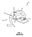
- Connector 10 comprises a housing 12 formed by sidewalls 14. A plurality of contacts 16 are soldered to corresponding contact pads 42, thereby securing the connector 10 to the PCB 40. When a plug 50 is inserted into the connector 10, the contacts 16 electrically couple the inserted plug 50 to one or more electrical circuits (not shown) disposed on the PCB 40.
- An impact tolerant connector of the present invention provides an improvement over the prior art connector 10 by allowing some displacement of the inserted plug 50 to reduce the stresses resulting from impact forces on the inserted plug 50.
- Impact tolerant connector 20 is mounted to PCB 40, and has a cavity 30 to receive and releasably retain the plug 50 upon insertion.
- Plug 50 may be a segmented plug, for example, a standard 2.5mm or 3.5mm plug that connects to the peripheral device (not shown) via cable 54.
- the peripheral device may be a hands-free headset for use with a wireless communications device, such as a mobile telephone.
- the segments on plug 50 may comprise a ground segment 56, an audio segment 58, and a microphone segment 60.
- Connector 20 may be used with many other types of plugs 50 connected to various types of peripheral devices. Examples of other peripheral devices that may include plug 50 include plug 50 include battery chargers and power supplies.
- plug 50 mates with connector 20, as shown in Figure 3 , by inserting plug 50 into the cavity 30, such that the plug 50 assumes an inserted position. In the inserted position, plug 50 couples a peripheral device to one or more electrical circuits disposed on the PCB 40.
- a user may communicate using the mobile telephone without having the mobile telephone in close proximity to the user's head.
- the connector 20 includes a housing 22 preferably constructed from a nonconductive, pliable material, such as plastic. However, those skilled in the art will realize that the material described herein is illustrative only, and any suitable material known in the art may be used to construct housing 22.
- Connector 20 further includes contacts 26 within cavity 30, as shown in Figure 4 , that electrically couple the inserted plug 50 to electrical circuits disposed on the PCB 40 by contacting the corresponding segments of inserted plug 50.
- the contacts 26 may be any contacts known in the art, and may be configured for surface mounting and/or through-hole mounting to PCB 40.
- Figure 5 illustrates an exemplary method of mounting connector 20 to PCB 40, as well as a more detailed view of the interaction between the contacts 26, openings 28, and the inserted plug 50.
- a contact 26 extends into the cavity 30 and engages the inserted plug 50, such that inserted plug 50 is urged into surface contact with the inner surface of the housing 22. This surface contact, which aids in the insertion alignment of the plug 50, helps to releasably retain the inserted plug 50 in the cavity 30.
- the contact 26 extends downward through housing 22 for attachment to the contact pad 42 of the PCB 40.
- contact 26 is shown in a surface mount configuration, it should be understood that it may also be adapted for through-hole mounting on the PCB 40.
- contact 26 may include a contact lead 34 that extends through the housing 22, and connects to optional mounting leads 32, which are in turn, secured to the additional contact pads 42. While not required, the mounting leads 32 add mounting stability and robustness to the connector 20.
- the housing 22 includes one or more openings 28 that permit displacement of the inserted plug 50 as a result of impact forces.
- the openings 28 formed in the sidewalls 24 are sized to yieldably retain the inserted plug 50 within the cavity 30.
- the size d 1 of the openings 28 is slightly smaller than the diameter d 2 of the inserted plug 50. This slight variation in the size of the openings 28 permits the inserted plug 50 to remain mated in the cavity 30 of connector 20 in the inserted position, and provides yielding resistance to the displacing movement of the inserted plug 50, as it displaces from the inserted position in response to the impact force.
- Figures 6a-6c illustrate examples of the angular displacements of the inserted plug 50 permitted by the illustrated embodiment.
- Figure 6a shows the substantially horizontal displacing force, F 2 , applied to the inserted plug 50, which causes the inserted portion of the inserted plug 50 to press against the opening 28.
- F 2 substantially horizontal displacing force
- the opening 28 provides at least partial resistance to the movement of the inserted plug 50.
- the displacing force F 2 reaches some threshold that threatens to break or crack the connector 20, or its corresponding connections to PCB 40, the opening 28 expands, allowing the inserted plug 50 to project through the opening 28 to assume a displaced position.
- connector 20 dissipates the impact forces by yieldably resisting the displacing movement of inserted plug 50, and permitting its partial angular displacement.
- the opening 28 may substantially conform to the shape of the inserted plug 50 as it projects through the opening 28. Further, upon removing the inserted plug 50 from the displaced position and re-inserting it into cavity 30, the opening 28 may return to its normal size and shape, due to the resiliency of the material.
- the displacing force F 2 resulted in an angular displacement that is generally horizontal with respect to the PCB 40.
- openings 28 may be disposed on any sidewall 24 in any orientation, thereby permitting angular displacements other than horizontal.
- generally vertical displacements with respect to the PCB 40 are shown in Figures 6b and 6c .
- the displacing force F 1 can be seen as a substantially vertical impacting force exerted on the inserted plug 50, resulting in the generally vertical displacement of the inserted plug 50 through the top opening 28. It is understood, however, that the present invention is not limited to the vertical and horizontal displacements illustrated herein, but rather, encompasses any displacement of the inserted plug 50 through the openings 28.
- any number of openings 28 may be disposed in the sidewalls 24 to facilitate various angles of displacement with respect to the PCB 40.
- Figure 7 illustrates an alternate embodiment of connector 20 having a substantially cylindrical housing 22.
- Plug 50 inserts into the cavity 30, while the one or more openings 28 permit the partial displacement of the inserted plug 50 through the openings 28.
- the one or more openings 28 need not be formed as cutouts in the sidewalls 24.
- FIG. 8 an exemplary embodiment of connector 20 is shown as it may be used in a wireless communications device, which is in this case, a mobile telephone 70.
- Mobile telephone 70 includes a display 84, a keypad 82, a speaker 86, a microphone 80, and the connector 20 of the present invention.
- the PCB 40 is encased within mobile telephone 70, and includes one or more electrical circuits disposed thereon.
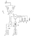
- FIG. 9 illustrates one embodiment of an electrical circuit, generally indicated by the number 100, wherein the connector 20 is configured for use as an audio jack.
- Electrical circuit 100 comprises a microprocessor 72 driven by a power source 94.
- Microprocessor 72 controls a digital signal processing circuit (DSP) 78, which is connected to a transmitter circuit 90 and a receiver circuit 88. Incoming and outgoing signals are transmitted and received via an antenna 92.
- DSP digital signal processing circuit
- An Input/Output (IO) circuit 76 connects the microphone 80, keypad 82, display 84, and speaker 86 to the microprocessor 72, as well as to an audio circuit 74, which is electrically coupled to connector 20 via contacts 26.
- DSP digital signal processing circuit
- plug 50 may be a segmented plug comprising a ground segment 56, an audio segment 58, and a microphone segment 60.
- at least three contacts 26 are disposed within cavity 30 to electrically couple each of the three segments 56, 58, and 60, to their corresponding contact points 42 on PCB 40. That is, the ground segment 56 couples to the ground circuit on the PCB 40, while the microphone and audio segments 58, 60, couple to the microphone and speaker circuits 80, 86 respectively.
- the plug 50 assumes the inserted position, the user may communicate with a remote party through the hands-free headset.
- openings 28 in the connector 20 permit the inserted plug 50 to displace from the inserted position to the displaced position. In this case, a user merely removes the displaced plug 50 from the connector 20, and re-inserts it.
- FIG. 10 illustrates an alternate embodiment wherein the connector 20 is configured for use as a power jack.
- connector 20 is coupled to a battery charging circuit 96 on the PCB 40, and may include only two contacts, ground and power (not shown).
- a peripheral device such as an external battery charger (not shown)
- a user may recharge the battery, or provide power to mobile telephone 70.
Landscapes
- Coupling Device And Connection With Printed Circuit (AREA)
- Telephone Set Structure (AREA)
Claims (31)
- Steckverbindung (20) zum Montieren auf einem gedruckten Schaltungsbrett (40), mit:einem Gehäuse (22) mit einer Einsetzöffnung, um einen Einsatz eines Steckers (50) zu erlauben;einem Empfangsraum (30) innerhalb des Gehäuses (12), um den eingesetzten Stecker (50) zu empfangen; undeiner Seitenöffnung (28) in einer Seitenwand des Gehäuses, dadurch gekennzeichnet, dass die Seitenöffnung (28) bemessen ist, um nachgebbar den eingesetzten Stecker festzuhalten und dadurch, dass die Seitenöffnung (28) sich in Reaktion auf eine Stoßkraft auf den eingesetzten Stecker (50) ausreichend ausdehnt, um einen Versatz des eingesetzten Steckers (50) durch die Seitenöffnung (28) zuzulassen.
- Steckverbindung nach Anspruch 1, wobei die Seitenöffnung (28) bezüglich eines Durchmessers des eingesetzten Steckers (50) unterbemessen ist.
- Steckverbindung nach Anspruch 1, weiter mit einem oder mehreren Kontakten (42), die innerhalb des Raumes (30) angeordnet sind, die elektrisch den eingesetzten Stecker (50) mit einer elektrischen Schaltung auf dem gedruckten Schaltungsbrett (40) koppeln.
- Steckverbindung nach Anspruch 3, wobei der eine oder die mehreren Kontakte (42) sich durch das Gehäuse (22) zum Montieren der Steckverbindung zu dem gedruckten Schaltungsbrett (40) erstrecken.
- Steckverbindung nach Anspruch 3, wobei der eine oder die mehreren Kontakte (42) den eingesetzten Stecker (50) in Oberflächenkontakt mit einer Innenoberfläche des Gehäuses (12) zwingen, um freigebbar den eingesetzten Stecker (50) festzuhalten.
- Steckverbindung nach Anspruch 1, wobei das Gehäuse (22) aus einem biegbaren Material konstruiert ist, das nachgebbar auf die Stoßkraft reagiert, die auf den eingesetzten Stecker (50) ausgeübt wird, was in der Ausdehnung der Seitenöffnung (48) resultiert, um den Versatz des eingesetzten Steckers (50) durch die Seitenöffnung zuzulassen.
- Steckverbindung nach Anspruch 1, wobei die Seitenöffnung als eine Aussparung in dem Gehäuse gebildet ist.
- Steckverbindung nach Anspruch 1, wobei die Seitenöffnung konfiguriert ist, einen Winkelversatz des eingesetzten Steckers bezüglich des gedruckten Schaltungsbrettes zuzulassen.
- Steckverbindung nach Anspruch 1, wobei die Seitenöffnung konfiguriert ist, einen horizontalen Versatz des eingesetzten Steckers bezüglich des gedruckten Schaltungsbrettes zuzulassen.
- Steckverbindung nach Anspruch 1, wobei die Seitenöffnung konfiguriert ist, einen vertikalen Versatz des eingesetzten Steckers bezüglich des gedruckten Schaltungsbrettes zuzulassen.
- Steckverbindung nach Anspruch 1, wobei das Gehäuse eine oder mehrere Seitenwände umfasst, und wobei die Öffnung eine erste Seitenöffnung ist, die als eine Aussparung in der einen oder mehreren Seitenwände gebildet ist.
- Steckverbindung nach Anspruch 11, weiter mit einer Vielzahl von Seitenöffnungen, wobei jede Seitenöffnung in der Vielzahl von Seitenöffnungen im Wesentlichen ähnlich zu der ersten Seitenöffnung ist.
- Steckverbindung nach Anspruch 12, wobei zumindest eine Seitenöffnung der Vielzahl von Seitenöffnungen.entlang einer vertikalen Ebene bezüglich des gedruckten Schaltungsbretts gebildet ist, um einen Vertikalversatz des eingesetzten Steckers durch die zumindest eine Seitenöffnung zuzulassen.
- Steckverbindung nach Anspruch 12, wobei zumindest eine Seitenöffnung in der Vielzahl von Seitenöffnungen entlang einer horizontalen Ebene bezüglich des gedruckten Schaltungsbretts gebildet ist, um einen horizontalen Versatz des eingesetzten Steckers durch die zumindest eine Seitenöffnung zuzulassen.
- Steckverbindung nach Anspruch 1, weiter mit einer Eingangsöffnung in dem Gehäuse, um den Stecker in dem Gehäuse zu empfangen.
- Steckverbindung nach Anspruch 15, wobei die Seitenöffnung in der Seitenwand des Gehäuses die Eingangsöffnung schneidet.
- Elektronisches Gerät, mit:einem gedruckten Schaltungsbrett (40) mit einer elektrischen Schaltung; undeiner Steckverbindung (20), die auf dem gedruckten Schaltungsbrett (40) montiert ist, wobei die Steckverbindung (20) umfasst:ein Gehäuse (12) mit einer Einsetzöffnung (30), um den Einsatz eines Steckers (50) zu erlauben;einen Empfangsraum (30) innerhalb des Gehäuses (12), um den eingesetzten Stecker (50) zu empfangen; undeine Seitenöffnung (28) in einer Seitenwand des Gehäuses (12), dadurch gekennzeichnet, dass die Seitenöffnung (28) bemessen ist, um nachgebbar den eingesetzten Stecker festzuhalten und dadurch, dass die Seitenöffnung (28) sich in Reaktion auf eine Stoßkraft auf den eingesetzten Stecker (50) ausreichend ausdehnt, um einen Versatz des eingesetzten Steckers (50) durch die Seitenöffnung (28) zuzulassen.
- Elektronisches Gerät nach Anspruch 17, wobei die Seitenöffnung bezüglich einem Durchmesser des eingesetzten Steckers (50) unterbemessen ist.
- Elektronisches Gerät nach Anspruch 17, weiter mit einem oder mehreren Kontakten, die innerhalb des Raumes angeordnet sind, die elektrisch den eingesetzten Stecker mit der elektrischen Schaltung koppeln.
- Elektronisches Gerät nach Anspruch 19, wobei der eine oder die mehreren Kontakte den eingesetzten Stecker in Oberflächenkontakt mit einer Innenoberfläche des Gehäuses zwingen, um freigebbar den eingesetzten Stecker festzuhalten.
- Elektronisches Gerät nach Anspruch 19, wobei der eingesetzte Stecker ein segmentierter Stecker einschließlich einer Vielzahl von Kontaktpunkten ist, und wobei der eine oder die mehreren Kontakte die Vielzahl von Kontaktpunkten mit der elektrischen Schaltung koppeln.
- Elektronisches Gerät nach Anspruch 17, wobei das Gehäuse aus einem biegbaren Material konstruiert ist, das nachgebbar auf die Stoßkraft reagiert, die auf den eingesetzten Stecker ausgeübt wird, was in der Ausdehnung der Seitenöffnung resultiert, um den Versatz des eingesetzten Steckers durch die-Seitenöffnung zu erlauben.
- Elektronisches Gerät nach Anspruch 17, wobei die Seitenöffnung als eine Aussparung in dem Gehäuse gebildet ist.
- Elektronisches Gerät nach Anspruch 17, wobei die Seitenöffnung konfiguriert ist, einen Winkelversatz des eingesetzten Steckers bezüglich des gedruckten Schaltungsbrettes zuzulassen.
- Elektronisches Gerät nach Anspruch 17, wobei die Seitenöffnung konfiguriert ist, einen horizontalen Versatz des eingesetzten Steckers bezüglich des gedruckten Schaltungsbrettes zuzulassen.
- Elektronisches Gerät nach Anspruch 17, wobei die Seitenöffnung konfiguriert ist, einen Winkelversatz des eingesetzten Steckers bezüglich des gedruckten Schaltungsbrettes zuzulassen.
- Elektronisches Gerät nach Anspruch 17, wobei das elektronische Gerät ein drahtloses Kommunikationsgerät umfasst.
- Elektronisches Gerät nach Anspruch 27, wobei das drahtlose Kommunikationsgerät ein Mobiltelefon ist.
- Verfahren eines Bereitstellens einer Spannungsentlastung für eine Brett-montierte Steckverbindung (20) mit einem Stecker (50), der in der Steckverbindung (20) eingesetzt ist, in Reaktion auf eine Stoßkraft, die auf den eingesetzten Stecker (50) ausgeübt wird, wobei das Verfahren umfasst:Einsetzen eines Steckers (50) durch eine Einsetzöffnung (28) in ein Gehäuse (12) der Steckverbindung (20),freigebbares Festhalten des eingesetzten Steckers (50) in einem Empfangsraum (30) innerhalb des Gehäuses (12) der Steckverbindung (20); undBereitstellen einer oder mehrerer flexibler Seitenöffnungen (28) in einer Seitenwand des Steckverbindungsgehäuses (12), das bemessen ist, um nachgebbar den eingesetzten Stecker (50) in einer Einsetzposition festzuhalten, wobei die Seitenöffnungen (28) sich in Reaktion auf die Stoßkraft ausreichend ausdehnen, um einen Versatz des eingesetzten Steckers (50) durch die eine oder mehrere Seitenöffnungen (28) zuzulassen.
- Verfahren nach Anspruch 29, wobei ein freigebbares Festhalten des eingesetzten Steckers (50) in dem Empfangsraum (30) ein Anordnen eines oder mehrerer Kontakte (42) in dem Empfangsraum (30) umfasst, um den eingesetzten Stecker (50) in einen Oberflächenkontakt mit einer Innenoberfläche des Steckverbindungsgehäuses (12) zu zwingen.
- Verfahren nach Anspruch 29, wobei die flexiblen Seitenöffnungen (28) Aussparungen in dem Steckverbindungsgehäuse (12) umfassen, die nachgebbar einem Versatz des eingesetzten Steckers (50) aus der eingesetzten Position zu einer versetzten Position bezüglich des gedruckten Schaltungsbrettes (40) widerstehen.
Applications Claiming Priority (3)
| Application Number | Priority Date | Filing Date | Title |
|---|---|---|---|
| US361243 | 2003-02-10 | ||
| US10/361,243 US6851975B2 (en) | 2003-02-10 | 2003-02-10 | Impact tolerant connector |
| PCT/IB2003/006235 WO2004070892A1 (en) | 2003-02-10 | 2003-12-30 | Impact tolerant connector |
Publications (2)
| Publication Number | Publication Date |
|---|---|
| EP1593186A1 EP1593186A1 (de) | 2005-11-09 |
| EP1593186B1 true EP1593186B1 (de) | 2010-02-10 |
Family
ID=32824176
Family Applications (1)
| Application Number | Title | Priority Date | Filing Date |
|---|---|---|---|
| EP03780484A Expired - Lifetime EP1593186B1 (de) | 2003-02-10 | 2003-12-30 | Stosstoleranter verbinder |
Country Status (7)
| Country | Link |
|---|---|
| US (1) | US6851975B2 (de) |
| EP (1) | EP1593186B1 (de) |
| JP (1) | JP4398872B2 (de) |
| CN (1) | CN100472893C (de) |
| AU (1) | AU2003288641A1 (de) |
| DE (1) | DE60331258D1 (de) |
| WO (1) | WO2004070892A1 (de) |
Families Citing this family (7)
| Publication number | Priority date | Publication date | Assignee | Title |
|---|---|---|---|---|
| KR100621015B1 (ko) * | 2004-10-13 | 2006-09-19 | 엘지전자 주식회사 | 이어폰 잭 및 이를 구비한 이동통신 단말기 |
| US20090170375A1 (en) * | 2007-12-26 | 2009-07-02 | Dayan Mervin A | Connector apparatus for video and audio signal transfer among multiple devices and system incorporating same |
| US20110117975A1 (en) * | 2009-11-17 | 2011-05-19 | Etymotic Research, Inc. | Two-Way Communication Device |
| KR20120080824A (ko) * | 2011-01-10 | 2012-07-18 | 삼성전자주식회사 | 휴대 단말기의 이어폰 커넥터 |
| US9176537B2 (en) | 2013-03-15 | 2015-11-03 | Intel Corporation | Connector assembly for an electronic device |
| KR102243235B1 (ko) * | 2014-08-14 | 2021-04-22 | 삼성전자주식회사 | 전자 장치, 그 제어 방법, 기록 매체 및 상기 전자 장치와 연동되는 이어잭 단자 캡 |
| US10312611B2 (en) * | 2017-03-30 | 2019-06-04 | Microsoft Technology Licensing, Llc | Connector for use with printed circuit board |
Family Cites Families (8)
| Publication number | Priority date | Publication date | Assignee | Title |
|---|---|---|---|---|
| US2480142A (en) * | 1945-09-21 | 1949-08-30 | Lager Fred | Electric contact |
| US3853377A (en) * | 1971-12-27 | 1974-12-10 | B Shlesinger | Tight fitting plug connection and method for making same |
| US5378161A (en) * | 1993-08-04 | 1995-01-03 | Minnesota Mining And Manufacturing Company | Tapered electrical connector |
| FR2719163A1 (fr) * | 1994-04-22 | 1995-10-27 | Amp France | Borne anti-corrosion par usure, destinée à recevoir une borne complémentaire. |
| US5482477A (en) * | 1994-06-28 | 1996-01-09 | The Whitaker Corporation | Micro-miniature coaxial connector with positive locking member |
| US5769652A (en) * | 1996-12-31 | 1998-06-23 | Applied Engineering Products, Inc. | Float mount coaxial connector |
| FR2795229B1 (fr) * | 1999-06-17 | 2001-08-03 | Ferraz | Machoire pour porte-fusible et porte-fusible equipe d'une telle machoire |
| US6540535B1 (en) * | 2001-11-09 | 2003-04-01 | Hon Hai Precision Ind. Co., Ltd. | Socket connector having resilient element for increasing contact force to inserted plug |
-
2003
- 2003-02-10 US US10/361,243 patent/US6851975B2/en not_active Expired - Lifetime
- 2003-12-30 WO PCT/IB2003/006235 patent/WO2004070892A1/en not_active Ceased
- 2003-12-30 AU AU2003288641A patent/AU2003288641A1/en not_active Abandoned
- 2003-12-30 DE DE60331258T patent/DE60331258D1/de not_active Expired - Lifetime
- 2003-12-30 EP EP03780484A patent/EP1593186B1/de not_active Expired - Lifetime
- 2003-12-30 CN CNB2003801096374A patent/CN100472893C/zh not_active Expired - Fee Related
- 2003-12-30 JP JP2004567832A patent/JP4398872B2/ja not_active Expired - Fee Related
Also Published As
| Publication number | Publication date |
|---|---|
| WO2004070892A1 (en) | 2004-08-19 |
| JP2006514403A (ja) | 2006-04-27 |
| CN100472893C (zh) | 2009-03-25 |
| US20040157489A1 (en) | 2004-08-12 |
| JP4398872B2 (ja) | 2010-01-13 |
| AU2003288641A1 (en) | 2004-08-30 |
| DE60331258D1 (de) | 2010-03-25 |
| CN1748345A (zh) | 2006-03-15 |
| EP1593186A1 (de) | 2005-11-09 |
| US6851975B2 (en) | 2005-02-08 |
Similar Documents
| Publication | Publication Date | Title |
|---|---|---|
| US6626706B2 (en) | Eight-pin electrical connector and USB connector | |
| EP0892468B1 (de) | Elektrische Verbinderanordnung mit Polarisationsmittel | |
| EP1511128B1 (de) | Achtpoliger-Audio-Steckbuchse-Verbinder mit reduzierten Abmessungen | |
| US9935388B2 (en) | Contact-support mechanism for increased retention force | |
| US6431901B1 (en) | I/O connector having an internal horizontal PCB | |
| CN101118993B (zh) | 薄型连接器 | |
| EP1632115B1 (de) | Tragbares elektronisches gerät mit flexibler verbindung zwischen interner elektronik und einer hilfsverbindung | |
| KR100619969B1 (ko) | 휴대 단말기의 이어잭 | |
| EP1593186B1 (de) | Stosstoleranter verbinder | |
| US6224409B1 (en) | Audio jack | |
| EP1648045A1 (de) | Batteriekontaktsystem und drahtloses Endgerät mit demselbem | |
| US6354870B1 (en) | Apparatus and method for mounting small electrical connector | |
| KR100772985B1 (ko) | 휴대폰 및 휴대용 음향기기의 이어폰 세트 | |
| US20040198444A1 (en) | Mobile phone IC card holder | |
| CN208285639U (zh) | Usb组件及电子设备 | |
| CN215497466U (zh) | 数据接头和数据传输线 | |
| US6200150B1 (en) | Flat-cable-type connector having auxiliary structure to enhance clamping force | |
| US7946858B2 (en) | Electrical plug and socket connector and plug thereof | |
| KR20040107056A (ko) | 이어폰 플러그의 접속장치 | |
| KR200248051Y1 (ko) | 휴대전화기용 충전 플러그의 결합구조 | |
| KR100454481B1 (ko) | 휴대전화기용 충전 플러그의 결합구조 | |
| EP1274217A1 (de) | Auftriebsgerät für ein mobiltelefon | |
| JP4111046B2 (ja) | 無線通信カードの着脱構造 | |
| KR20050070324A (ko) | 단락 방지용 배터리 접지부 구조 | |
| KR200233495Y1 (ko) | 휴대용 단말기 |
Legal Events
| Date | Code | Title | Description |
|---|---|---|---|
| PUAI | Public reference made under article 153(3) epc to a published international application that has entered the european phase |
Free format text: ORIGINAL CODE: 0009012 |
|
| 17P | Request for examination filed |
Effective date: 20050808 |
|
| AK | Designated contracting states |
Kind code of ref document: A1 Designated state(s): AT BE BG CH CY CZ DE DK EE ES FI FR GB GR HU IE IT LI LU MC NL PT RO SE SI SK TR |
|
| AX | Request for extension of the european patent |
Extension state: AL LT LV MK |
|
| DAX | Request for extension of the european patent (deleted) | ||
| RBV | Designated contracting states (corrected) |
Designated state(s): DE FR GB |
|
| RIC1 | Information provided on ipc code assigned before grant |
Ipc: H01R 12/16 20060101AFI20090430BHEP |
|
| GRAJ | Information related to disapproval of communication of intention to grant by the applicant or resumption of examination proceedings by the epo deleted |
Free format text: ORIGINAL CODE: EPIDOSDIGR1 |
|
| GRAP | Despatch of communication of intention to grant a patent |
Free format text: ORIGINAL CODE: EPIDOSNIGR1 |
|
| GRAS | Grant fee paid |
Free format text: ORIGINAL CODE: EPIDOSNIGR3 |
|
| GRAA | (expected) grant |
Free format text: ORIGINAL CODE: 0009210 |
|
| AK | Designated contracting states |
Kind code of ref document: B1 Designated state(s): DE FR GB |
|
| REG | Reference to a national code |
Ref country code: GB Ref legal event code: FG4D |
|
| REF | Corresponds to: |
Ref document number: 60331258 Country of ref document: DE Date of ref document: 20100325 Kind code of ref document: P |
|
| PLBE | No opposition filed within time limit |
Free format text: ORIGINAL CODE: 0009261 |
|
| STAA | Information on the status of an ep patent application or granted ep patent |
Free format text: STATUS: NO OPPOSITION FILED WITHIN TIME LIMIT |
|
| 26N | No opposition filed |
Effective date: 20101111 |
|
| REG | Reference to a national code |
Ref country code: FR Ref legal event code: PLFP Year of fee payment: 13 |
|
| REG | Reference to a national code |
Ref country code: FR Ref legal event code: PLFP Year of fee payment: 14 |
|
| PGFP | Annual fee paid to national office [announced via postgrant information from national office to epo] |
Ref country code: GB Payment date: 20161228 Year of fee payment: 14 |
|
| REG | Reference to a national code |
Ref country code: FR Ref legal event code: PLFP Year of fee payment: 15 |
|
| PGFP | Annual fee paid to national office [announced via postgrant information from national office to epo] |
Ref country code: FR Payment date: 20171127 Year of fee payment: 15 |
|
| GBPC | Gb: european patent ceased through non-payment of renewal fee |
Effective date: 20171230 |
|
| PG25 | Lapsed in a contracting state [announced via postgrant information from national office to epo] |
Ref country code: GB Free format text: LAPSE BECAUSE OF NON-PAYMENT OF DUE FEES Effective date: 20171230 |
|
| PG25 | Lapsed in a contracting state [announced via postgrant information from national office to epo] |
Ref country code: FR Free format text: LAPSE BECAUSE OF NON-PAYMENT OF DUE FEES Effective date: 20181231 |
|
| PGFP | Annual fee paid to national office [announced via postgrant information from national office to epo] |
Ref country code: DE Payment date: 20201216 Year of fee payment: 18 |
|
| REG | Reference to a national code |
Ref country code: DE Ref legal event code: R119 Ref document number: 60331258 Country of ref document: DE |
|
| PG25 | Lapsed in a contracting state [announced via postgrant information from national office to epo] |
Ref country code: DE Free format text: LAPSE BECAUSE OF NON-PAYMENT OF DUE FEES Effective date: 20220701 |