EP1593157B1 - Technique for sizing and positioning power switches in an integrated circuit - Google Patents
Technique for sizing and positioning power switches in an integrated circuit Download PDFInfo
- Publication number
- EP1593157B1 EP1593157B1 EP04707972A EP04707972A EP1593157B1 EP 1593157 B1 EP1593157 B1 EP 1593157B1 EP 04707972 A EP04707972 A EP 04707972A EP 04707972 A EP04707972 A EP 04707972A EP 1593157 B1 EP1593157 B1 EP 1593157B1
- Authority
- EP
- European Patent Office
- Prior art keywords
- power
- voltage
- power switches
- size
- area
- Prior art date
- Legal status (The legal status is an assumption and is not a legal conclusion. Google has not performed a legal analysis and makes no representation as to the accuracy of the status listed.)
- Expired - Lifetime
Links
- 238000000034 method Methods 0.000 title claims description 14
- 238000004513 sizing Methods 0.000 title 1
- 230000001419 dependent effect Effects 0.000 abstract description 5
- 238000005516 engineering process Methods 0.000 description 8
- 239000002184 metal Substances 0.000 description 8
- 238000005457 optimization Methods 0.000 description 2
- XUIMIQQOPSSXEZ-UHFFFAOYSA-N Silicon Chemical compound [Si] XUIMIQQOPSSXEZ-UHFFFAOYSA-N 0.000 description 1
- 238000013459 approach Methods 0.000 description 1
- 238000001816 cooling Methods 0.000 description 1
- 230000007423 decrease Effects 0.000 description 1
- 230000003247 decreasing effect Effects 0.000 description 1
- 230000010354 integration Effects 0.000 description 1
- 238000004806 packaging method and process Methods 0.000 description 1
- 230000002093 peripheral effect Effects 0.000 description 1
- 239000004065 semiconductor Substances 0.000 description 1
- 229910052710 silicon Inorganic materials 0.000 description 1
- 239000010703 silicon Substances 0.000 description 1
Images


Classifications
-
- H—ELECTRICITY
- H01—ELECTRIC ELEMENTS
- H01L—SEMICONDUCTOR DEVICES NOT COVERED BY CLASS H10
- H01L27/00—Devices consisting of a plurality of semiconductor or other solid-state components formed in or on a common substrate
-
- H—ELECTRICITY
- H01—ELECTRIC ELEMENTS
- H01L—SEMICONDUCTOR DEVICES NOT COVERED BY CLASS H10
- H01L27/00—Devices consisting of a plurality of semiconductor or other solid-state components formed in or on a common substrate
- H01L27/02—Devices consisting of a plurality of semiconductor or other solid-state components formed in or on a common substrate including semiconductor components specially adapted for rectifying, oscillating, amplifying or switching and having at least one potential-jump barrier or surface barrier; including integrated passive circuit elements with at least one potential-jump barrier or surface barrier
- H01L27/04—Devices consisting of a plurality of semiconductor or other solid-state components formed in or on a common substrate including semiconductor components specially adapted for rectifying, oscillating, amplifying or switching and having at least one potential-jump barrier or surface barrier; including integrated passive circuit elements with at least one potential-jump barrier or surface barrier the substrate being a semiconductor body
- H01L27/10—Devices consisting of a plurality of semiconductor or other solid-state components formed in or on a common substrate including semiconductor components specially adapted for rectifying, oscillating, amplifying or switching and having at least one potential-jump barrier or surface barrier; including integrated passive circuit elements with at least one potential-jump barrier or surface barrier the substrate being a semiconductor body including a plurality of individual components in a repetitive configuration
- H01L27/118—Masterslice integrated circuits
- H01L27/11898—Input and output buffer/driver structures
-
- H—ELECTRICITY
- H01—ELECTRIC ELEMENTS
- H01L—SEMICONDUCTOR DEVICES NOT COVERED BY CLASS H10
- H01L27/00—Devices consisting of a plurality of semiconductor or other solid-state components formed in or on a common substrate
- H01L27/02—Devices consisting of a plurality of semiconductor or other solid-state components formed in or on a common substrate including semiconductor components specially adapted for rectifying, oscillating, amplifying or switching and having at least one potential-jump barrier or surface barrier; including integrated passive circuit elements with at least one potential-jump barrier or surface barrier
- H01L27/0203—Particular design considerations for integrated circuits
- H01L27/0207—Geometrical layout of the components, e.g. computer aided design; custom LSI, semi-custom LSI, standard cell technique
Definitions
- the present invention generally relates to integrated circuits and more particularly to an improved integrated circuit design and method which utilizes voltage islands in application specific integrated circuit (ASIC) designs that make increasing use of power supply switching techniques to control chip power consumption.
- ASIC application specific integrated circuit
- the total power consumed by conventional CMOS circuitry includes active power consumed by circuits as they switch states and either charge or discharge the capacitance associated with the switching nodes.
- Active power represents the power consumed by the intended work of the circuit to switch signal states and thus execute logic function. This power is not present if the circuit in question is not actively switching. Active power is proportional to the capacitance that is switched, the frequency of operation and to the square of the power supply voltage. Due to technology scaling, the capacitance per unit area increases with each process generation. The power increase represented by this capacitance increase is offset by the scaling of the power supply voltage, Vdd.
- Patent Abstracts of Japan vol.014, no.213 (E-0923), 7 May 1990 & JP 02049449A (Fujitsu Ltd), 19 February 1990 teaches increasing the operating speed of a logical circuit by a method wherein signals outputted by a logical circuit emitter follower section are led to an output electrode pad through a current switch section and an emitter follower transistor receiving the output.
- EP-A-0288803 (IBM) 2 November 1988 , teaches personalizable chips for analog and analog/digital circuits.
- Patent Abstracts of Japan vol.001, no.165 (E-079), 26 December 1977 & JP 52111389A (NEC Corp), 19 September 1977 teaches the changing of the total power ratio generated inside and outside to minimize the power consumption of invertors.
- the invention provides a method as claimed in claim 1.
- SoC system-on-a-chip
- An SoC architecture based on Voltage Islands uses additional design components such as power switches to distribute and manage power.
- ASIC designs are making increasing use of power supply switching techniques to control chip power consumption. Thus, power can be conserved by switching off certain voltage islands when they are idle.
- This invention provides a solution to the problem of optimum placement of such power supply switch circuits.
- Figure 1 shows an integrated circuit which may include a number of isolated blocks, one of which is labeled "Voltage Island" 10.
- the power supply of the circuitry within the boundary of the box 10 is isolated from the remainder of the chip and controlled by the power switch circuit 11.
- this particular example describes the island power coming from a single peripheral I/O cell 12, through the power switch 11, then distributed to all cells within the island.
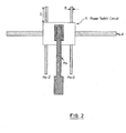
- FIG. 2 shows a power switch circuit 11 incorporated into integrated circuit wiring.
- the highest level of metal shown (Mx) provides unswitched current to the power switch circuit.
- the power switch 11 supplies switched current to the voltage island via the underlying metal layers, MX-1 and MX-2 in this example.
- the current capacity of the power switch cell is limited by wire width or the circuit providing the switching function. In either case, each power switch cell has limited current capacity, a portion of which is available on MX-1 and the remainder on MX-2. If the current capacity of the orthogonal metal lines driven by the power switch cell is equivalent, equal current is available on each metal level. If properly designed, current density does not exceed the capacity of the metal wire and voltage drop (voltage drop increases with distance driven) is the limiting factor to how far from the power switch cell a circuit can be driven.
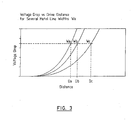
- Figure 3 shows a series of curves depicting the relationship between voltage drop and maximum drive distance for a given load of various width metal lines on a single periodicity (illustrated as Wa, Wb and Wc).
- Wa is the narrowest line and Wc is the widest line in Figure 3 .
- the curves represent a particular power pattern and load, but generally voltage drop increases with distance driven.
- the invention matches the size of the power switch to provide just the current supported by the power bus width available. Thus, by knowing the wiring length, width and load, the current and voltage that will be present on the power buses can be calculated.
- the size of the power switch within the voltage island is selected to match this current and voltage. Matching the power switch circuit size with the power bus width assures that the minimum area overhead is devoted to power switching circuits.
- the efficient placement of the power switch cells within a voltage island is dependent on the circuitry within the island.
- the effective support area of a power switch cell is tightly coupled to the design of the power bus it drives.
- the effective support area of a power switch can be approximated as a circle of radius equal to the maximum drive distance shown in Figure 3 .
- Figure 4 shows the translation from maximum drive distance to effective area.
- One half the dimension of a side of the effective support area is the effective device distance.
- the relationship is design dependent related to the number of metal levels available for power distribution and their geometric relationship.
- the invention is applicable to any design style in which the placement of a power switch circuit can be related to a serviceable area.
- Figure 5 shows a Voltage Island with Uniform Random Logic Placement and power consumption.
- the embodiment determines the current and voltage drop that will occur on the power buses. From this, the embodiment selects the appropriate size power switch.
- the embodiment determines the maximum power switch drive distance for the power bus width and distribution as shown above.
- the embodiment then divides the voltage island area by the power switch serviceable area to determine the number of power switch cells needed.
- the embodiment evenly distributes the power switch circuits across the voltage island making sure the drive distance does not exceed x or y in Figure 5 (x and y are the maximum power switch serviceable area for the given power bus width and distribution).
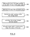
- the embodiment matches the size of the power switches to the width of one or more power buses supplying power to the voltage island 800.
- the matching process 800 matches the size of the power switches to the current and voltage that will be provided by the power buses.
- the embodiment determines the size of the serviceable area to which each of the power switches can provide power 802.
- the serviceable area is dependent upon power bus current, voltage drop, and distribution.
- the embodiment places the power switches within the voltage island according to the size of the serviceable area of each of the power switches 804. More specifically, the embodiment divides the voltage island area by the size of serviceable area to calculate the number of power switches needed.
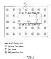
- Figure 6 shows a voltage island with non- uniform placement having a logic core 60 having dimensions P by Q.
- the embodiment again determines the voltage drop and the switch size 800.
- the embodiment determines the maximum power switch drive distance (e.g. serviceable area) for the voltage island power bus distribution for the non-core portion 61 of the island 802.
- the area of the logic core(s) 60 is subtracted from the entire voltage island area to calculate the non-core 61 area.
- the embodiment then evenly distributes the power switch cells across the non-core area (labeled U in Fig. 6 ) 804.
- the embodiment calculates the serviceable area and the number of power switches needed relative to the logic core 60 area (by dividing the logic core area by the power switch serviceable area) 806. The embodiment then allocates (positions, distributes, etc.) this number of power switch circuits evenly along the sides of the core 60, as shown in item 808. More specifically, the power switch circuits for the core area C are positioned along the longer sides of the core 60. This minimizes the distance between the power switches to ensure adequate power supply to all areas of the logic core 60.
- additional power switch cells are added to the extent additional power buses are available.
- An example of such extra power switches Ca are shown in Figure 7 .
- the supported drive distance increases by the proportion of additional power switch cells Ca added. Placement of the additional cells is again along the periphery of the longer side of the logic core, as explained above.
- This technique can be further supplemented by increasing the power bus width within the core area thereby increasing the size of the power switches and the power switch serviceable area.
- the embodiment produces structures shown in Figures 5-7 that include at least one voltage island 10 and a pattern of power switches 11 within the voltage island.
- the pattern 11 balances the power switches according to the size of the serviceable area to which each of the power switches can provide power.
- Power buses MX-1, MX-2 are connected to the power switches 11.
- the size of the power switches 11 are matched to the current and voltage that will be provided by the power buses MX.
- the size of the serviceable area to which each of the power switches can provide power is dependent upon the size of the power switches and the power bus width. Thus, larger power switches have a larger serviceable area than smaller power switches.
- the number of power switches is equal to the area of the voltage island divided by the size of serviceable area.
- the structure can include a number of logic core areas (although only one (60) is shown for clarity) within the voltage island.
- a sub-group of the power switches (C,Ca) is positioned along the periphery of logic core areas.
- the logic core areas generally comprise rectangles having a longer pair of sides and a shorter pair of sides.
- the power switches are positioned along the longer sides of the logic core areas to minimize the distance between switches, as explained above.
- the embodiment determines the quantity of power switch cells required and provides a technique for analysis and placement to minimize the number of power switch cells. Placement is driven by power bus design and circuit power consumption.
- the power switch cells can be distributed unevenly so that different areas (having different power needs) within a given voltage island could be treated separately. Higher densities of power switch cells could be placed in areas of higher power density. This would create an uneven distribution of power switch cells across the voltage island. In the vicinity of cores, placement is along two opposite sides only. In the overall picture, several schemes can be used to evenly distribute power switch cells in localized regions of the voltage island to result in an uneven distribution across the voltage island. Therefore, this allows each area of the voltage island to be treated according to its specific needs, thereby only utilizing power switch cells where needed. This minimizes the number of power switch cells that are used in the design and also reduces power consumption.
Landscapes
- Engineering & Computer Science (AREA)
- Power Engineering (AREA)
- Physics & Mathematics (AREA)
- Condensed Matter Physics & Semiconductors (AREA)
- General Physics & Mathematics (AREA)
- Computer Hardware Design (AREA)
- Microelectronics & Electronic Packaging (AREA)
- General Engineering & Computer Science (AREA)
- Semiconductor Integrated Circuits (AREA)
- Design And Manufacture Of Integrated Circuits (AREA)
Abstract
Description
- The present invention generally relates to integrated circuits and more particularly to an improved integrated circuit design and method which utilizes voltage islands in application specific integrated circuit (ASIC) designs that make increasing use of power supply switching techniques to control chip power consumption.
- As technology scales for increased circuit density and performance, the need to reduce power consumption increases in significance as designers strive to utilize the advancing silicon capabilities. The consumer product market further drives the need to minimize chip power consumption.
- The total power consumed by conventional CMOS circuitry includes active power consumed by circuits as they switch states and either charge or discharge the capacitance associated with the switching nodes. Active power represents the power consumed by the intended work of the circuit to switch signal states and thus execute logic function. This power is not present if the circuit in question is not actively switching. Active power is proportional to the capacitance that is switched, the frequency of operation and to the square of the power supply voltage. Due to technology scaling, the capacitance per unit area increases with each process generation. The power increase represented by this capacitance increase is offset by the scaling of the power supply voltage, Vdd.
- The frequency of operation, however, increases with each generation, leading to an overall increase in active power density from technology generation to technology generation. This increasing power density in turn drives the need for more expensive packaging, complex cooling solutions and decreased reliability due to increased temperatures.
- Patent Abstracts of Japan vol.014, no.213 (E-0923), 7 May 1990 &
JP 02049449A (Fujitsu Ltd), 19 February 1990 -
EP-A-0288803 (IBM) 2 November 1988 , teaches personalizable chips for analog and analog/digital circuits. -
US-A-5256893 (Yasuoka Hideki) 26 October 1993 , teaches an integrated circuit device with power MUSFET. - Patent Abstracts of Japan vol.001, no.165 (E-079), 26 December 1977 &
JP 52111389A (NEC Corp), 19 September 1977 - Therefore, there is a need for a method that increases performance, while at the same time decreases power consumption. The invention described below satisfies these by providing a solution to the problem of optimum placement of power supply switch circuits.
- The invention provides a method as claimed in
claim 1. - The invention will be better understood from the following detailed description of preferred embodiments of the invention with reference to the drawings, in which:
-
Fig. 1 is an integrated circuit which includes an number of isolated blocks; -
Fig. 2 is a power switch circuit incorporated into the integrated circuit wiring; -
Fig. 3 shows a series of curves that depicts the relationship between voltage drop and maximum drive distance for various width metal lines; -
Fig. 4 shows the translation from drive distance to effective area; -
Fig. 5 shows a Voltage Island with Uniform Random Logic Placement; -
Figs. 6 and7 shows the structure which can include a number of logic core areas within the voltage island; and -
Fig. 8 is a flowchart showing how the invention matches the size of the power switches to the width of one or more power buses. - The power challenges posed by advanced technologies force system designers to make choices concerning devices, structures and voltage levels for the functions they are designing. In previous generations, large functional blocks were not integrated on the same chip, so these choices could be made independently for each block. High levels of integration supported by system-on-a-chip (SoC) enabling technology drive single chip implementations, where traditional approaches to power distribution and performance optimization fail to provide the flexibility of voltage and technology optimization of the previously disintegrated solution.
- Newer technologies divide each semiconductor chip into individual functional blocks (voltage islands) as explained in copending
U.S. andPatent Application Number 10/065,20110/065,202 - An SoC architecture based on Voltage Islands uses additional design components such as power switches to distribute and manage power. ASIC designs are making increasing use of power supply switching techniques to control chip power consumption. Thus, power can be conserved by switching off certain voltage islands when they are idle. This invention provides a solution to the problem of optimum placement of such power supply switch circuits.
- More specifically,
Figure 1 shows an integrated circuit which may include a number of isolated blocks, one of which is labeled "Voltage Island" 10. The power supply of the circuitry within the boundary of thebox 10 is isolated from the remainder of the chip and controlled by thepower switch circuit 11. For ease of description, this particular example describes the island power coming from a single peripheral I/O cell 12, through thepower switch 11, then distributed to all cells within the island. - However, a single I/
O cell 12, connectingwire 13, andpower switch cell 11 has limited current capacity. Thus, to fully exploit the advantages of power supply switching, it is better to use multiple power switch circuits in each voltage island. The following describes a technique for determining the quantity of power switch cells required and their placement for varied voltage island content. -
Figure 2 shows apower switch circuit 11 incorporated into integrated circuit wiring. In this example, the highest level of metal shown (Mx) provides unswitched current to the power switch circuit. Thepower switch 11 supplies switched current to the voltage island via the underlying metal layers, MX-1 and MX-2 in this example. The current capacity of the power switch cell is limited by wire width or the circuit providing the switching function. In either case, each power switch cell has limited current capacity, a portion of which is available on MX-1 and the remainder on MX-2. If the current capacity of the orthogonal metal lines driven by the power switch cell is equivalent, equal current is available on each metal level. If properly designed, current density does not exceed the capacity of the metal wire and voltage drop (voltage drop increases with distance driven) is the limiting factor to how far from the power switch cell a circuit can be driven. -
Figure 3 shows a series of curves depicting the relationship between voltage drop and maximum drive distance for a given load of various width metal lines on a single periodicity (illustrated as Wa, Wb and Wc). Wa is the narrowest line and Wc is the widest line inFigure 3 . The curves represent a particular power pattern and load, but generally voltage drop increases with distance driven. The invention matches the size of the power switch to provide just the current supported by the power bus width available. Thus, by knowing the wiring length, width and load, the current and voltage that will be present on the power buses can be calculated. The size of the power switch within the voltage island is selected to match this current and voltage. Matching the power switch circuit size with the power bus width assures that the minimum area overhead is devoted to power switching circuits. - The efficient placement of the power switch cells within a voltage island is dependent on the circuitry within the island. The effective support area of a power switch cell is tightly coupled to the design of the power bus it drives. For regular orthogonal power distribution, the effective support area of a power switch can be approximated as a circle of radius equal to the maximum drive distance shown in
Figure 3 .Figure 4 shows the translation from maximum drive distance to effective area. One half the dimension of a side of the effective support area is the effective device distance. The relationship is design dependent related to the number of metal levels available for power distribution and their geometric relationship. The invention is applicable to any design style in which the placement of a power switch circuit can be related to a serviceable area. -
Figure 5 shows a Voltage Island with Uniform Random Logic Placement and power consumption. First, the embodiment determines the current and voltage drop that will occur on the power buses. From this, the embodiment selects the appropriate size power switch. Next, the embodiment determines the maximum power switch drive distance for the power bus width and distribution as shown above. The embodiment then divides the voltage island area by the power switch serviceable area to determine the number of power switch cells needed. The embodiment evenly distributes the power switch circuits across the voltage island making sure the drive distance does not exceed x or y inFigure 5 (x and y are the maximum power switch serviceable area for the given power bus width and distribution). - In other words, as shown in
Figure 8 , the embodiment matches the size of the power switches to the width of one or more power buses supplying power to thevoltage island 800. Thematching process 800 matches the size of the power switches to the current and voltage that will be provided by the power buses. The embodiment then determines the size of the serviceable area to which each of the power switches can providepower 802. The serviceable area is dependent upon power bus current, voltage drop, and distribution. Next, the embodiment places the power switches within the voltage island according to the size of the serviceable area of each of the power switches 804. More specifically, the embodiment divides the voltage island area by the size of serviceable area to calculate the number of power switches needed. - However, uniform power switch placement is not always possible, such as the case of a large core within an island. For example,
Figure 6 shows a voltage island with non- uniform placement having alogic core 60 having dimensions P by Q. First, the embodiment again determines the voltage drop and theswitch size 800. Next, the embodiment determines the maximum power switch drive distance (e.g. serviceable area) for the voltage island power bus distribution for thenon-core portion 61 of theisland 802. The area of the logic core(s) 60 is subtracted from the entire voltage island area to calculate the non-core 61 area. The embodiment then evenly distributes the power switch cells across the non-core area (labeled U inFig. 6 ) 804. Again, the embodiment calculates the serviceable area and the number of power switches needed relative to thelogic core 60 area (by dividing the logic core area by the power switch serviceable area) 806. The embodiment then allocates (positions, distributes, etc.) this number of power switch circuits evenly along the sides of the core 60, as shown initem 808. More specifically, the power switch circuits for the core area C are positioned along the longer sides of thecore 60. This minimizes the distance between the power switches to ensure adequate power supply to all areas of thelogic core 60. - If the shorter core dimension P exceeds twice the effective drive distance or if the distance between the power switches is greater than twice the effective drive distance (2x or 2y), additional power switch cells are added to the extent additional power buses are available. An example of such extra power switches Ca are shown in
Figure 7 . The supported drive distance increases by the proportion of additional power switch cells Ca added. Placement of the additional cells is again along the periphery of the longer side of the logic core, as explained above. This technique can be further supplemented by increasing the power bus width within the core area thereby increasing the size of the power switches and the power switch serviceable area. - The embodiment produces structures shown in
Figures 5-7 that include at least onevoltage island 10 and a pattern of power switches 11 within the voltage island. Thepattern 11 balances the power switches according to the size of the serviceable area to which each of the power switches can provide power. Power buses MX-1, MX-2 are connected to the power switches 11. As explained above, the size of the power switches 11 are matched to the current and voltage that will be provided by the power buses MX. The size of the serviceable area to which each of the power switches can provide power is dependent upon the size of the power switches and the power bus width. Thus, larger power switches have a larger serviceable area than smaller power switches. As shown above, the number of power switches is equal to the area of the voltage island divided by the size of serviceable area. - As shown in
Figures 6 and7 , the structure can include a number of logic core areas (although only one (60) is shown for clarity) within the voltage island. A sub-group of the power switches (C,Ca) is positioned along the periphery of logic core areas. The logic core areas generally comprise rectangles having a longer pair of sides and a shorter pair of sides. The power switches are positioned along the longer sides of the logic core areas to minimize the distance between switches, as explained above. - Thus, as shown above, the embodiment determines the quantity of power switch cells required and provides a technique for analysis and placement to minimize the number of power switch cells. Placement is driven by power bus design and circuit power consumption.
- Further, the power switch cells can be distributed unevenly so that different areas (having different power needs) within a given voltage island could be treated separately. Higher densities of power switch cells could be placed in areas of higher power density. This would create an uneven distribution of power switch cells across the voltage island. In the vicinity of cores, placement is along two opposite sides only. In the overall picture, several schemes can be used to evenly distribute power switch cells in localized regions of the voltage island to result in an uneven distribution across the voltage island. Therefore, this allows each area of the voltage island to be treated according to its specific needs, thereby only utilizing power switch cells where needed. This minimizes the number of power switch cells that are used in the design and also reduces power consumption.
Claims (1)
- A method of positioning power switches (11) in a voltage island (10) of an integrated circuit structure, said voltage island being one of a plurality of functional blocks of the integrated circuit structure wherein each function block can have unique power characteristics, said method characterised by comprising steps of:determining the current and the voltage that will be present on a power bus supplying power to said voltage island, based on the wiring length, width and load of the power bus;matching (800) the size of said power switches (11) to the determined current and voltage;determining (802) the size of the serviceable area to which each of the power switches can provide power, based upon power bus current, voltage and distribution;determining (806) the number of power switches required by dividing the voltage island area by the size of the serviceable area;placing (804) said determined number of power switches within said voltage island, including allocating a group of said power switches along the periphery of logic core areas within said voltage island.
Applications Claiming Priority (3)
| Application Number | Priority Date | Filing Date | Title |
|---|---|---|---|
| US10/248,696 US6924661B2 (en) | 2003-02-10 | 2003-02-10 | Power switch circuit sizing technique |
| US248696 | 2003-02-10 | ||
| PCT/GB2004/000434 WO2004070773A2 (en) | 2003-02-10 | 2004-02-04 | Integrated circuit power switch circuit sizing and placement technique |
Publications (2)
| Publication Number | Publication Date |
|---|---|
| EP1593157A2 EP1593157A2 (en) | 2005-11-09 |
| EP1593157B1 true EP1593157B1 (en) | 2011-05-11 |
Family
ID=32823584
Family Applications (1)
| Application Number | Title | Priority Date | Filing Date |
|---|---|---|---|
| EP04707972A Expired - Lifetime EP1593157B1 (en) | 2003-02-10 | 2004-02-04 | Technique for sizing and positioning power switches in an integrated circuit |
Country Status (8)
| Country | Link |
|---|---|
| US (1) | US6924661B2 (en) |
| EP (1) | EP1593157B1 (en) |
| JP (1) | JP4566186B2 (en) |
| KR (1) | KR100734999B1 (en) |
| CN (1) | CN100370613C (en) |
| AT (1) | ATE509371T1 (en) |
| TW (1) | TWI276948B (en) |
| WO (1) | WO2004070773A2 (en) |
Families Citing this family (9)
| Publication number | Priority date | Publication date | Assignee | Title |
|---|---|---|---|---|
| JP3770836B2 (en) * | 2002-01-23 | 2006-04-26 | 株式会社ルネサステクノロジ | Logic circuit capable of turning on / off power switch at high speed and current reduction method in the logic circuit |
| US8304813B2 (en) * | 2007-01-08 | 2012-11-06 | SanDisk Technologies, Inc. | Connection between an I/O region and the core region of an integrated circuit |
| JP4834625B2 (en) * | 2007-07-31 | 2011-12-14 | 株式会社東芝 | Power management apparatus and power management method |
| US7904838B2 (en) * | 2007-08-15 | 2011-03-08 | Ati Technologies Ulc | Circuits with transient isolation operable in a low power state |
| CN103577621B (en) * | 2012-08-08 | 2017-06-23 | 扬智科技股份有限公司 | The layout method of chip and its power switch circuit |
| JP2015069333A (en) * | 2013-09-27 | 2015-04-13 | 富士通セミコンダクター株式会社 | Design method and design program |
| US9058459B1 (en) * | 2013-12-30 | 2015-06-16 | Samsung Electronics Co., Ltd. | Integrated circuit layouts and methods to reduce leakage |
| US9824174B2 (en) * | 2015-09-11 | 2017-11-21 | Qualcomm Incorporated | Power-density-based clock cell spacing |
| CN111104771B (en) * | 2018-10-26 | 2021-09-21 | 珠海格力电器股份有限公司 | Method and device for placing power off unit |
Family Cites Families (17)
| Publication number | Priority date | Publication date | Assignee | Title |
|---|---|---|---|---|
| JPS52111389A (en) * | 1976-03-16 | 1977-09-19 | Nec Corp | Iil-type semi-conductor ic |
| JPH0817227B2 (en) * | 1987-04-30 | 1996-02-21 | インターナシヨナル・ビジネス・マシーンズ・コーポレーシヨン | Semiconductor chips that can be personalized |
| US5256893A (en) * | 1987-07-22 | 1993-10-26 | Hitachi, Ltd. | Semiconductor integrated circuit device with power MOSFET incorporated |
| JPH0249449A (en) * | 1989-06-23 | 1990-02-19 | Fujitsu Ltd | Semiconductor integrated circuit device |
| US5689428A (en) | 1990-09-28 | 1997-11-18 | Texas Instruments Incorporated | Integrated circuits, transistors, data processing systems, printed wiring boards, digital computers, smart power devices, and processes of manufacture |
| JPH0521713A (en) * | 1991-07-09 | 1993-01-29 | Mitsubishi Electric Corp | Semiconductor integrated circuit device |
| US5311058A (en) | 1991-11-29 | 1994-05-10 | Trw Inc. | Integrated circuit power distribution system |
| WO1995017007A1 (en) | 1993-12-14 | 1995-06-22 | Oki America, Inc. | Efficient routing method and resulting structure for integrated circuits |
| US5668389A (en) | 1994-12-02 | 1997-09-16 | Intel Corporation | Optimized power bus structure |
| JP3869045B2 (en) | 1995-11-09 | 2007-01-17 | 株式会社日立製作所 | Semiconductor memory device |
| US6091090A (en) | 1997-09-19 | 2000-07-18 | In-Chip Systems, Inc. | Power and signal routing technique for gate array design |
| US6072740A (en) | 1997-12-01 | 2000-06-06 | Intel Corporation | Apparatus for reducing the effects of power supply distribution related noise |
| JP4498500B2 (en) * | 1999-10-06 | 2010-07-07 | 株式会社ルネサステクノロジ | Semiconductor device |
| US6396137B1 (en) * | 2000-03-15 | 2002-05-28 | Kevin Mark Klughart | Integrated voltage/current/power regulator/switch system and method |
| JP4963144B2 (en) * | 2000-06-22 | 2012-06-27 | ルネサスエレクトロニクス株式会社 | Semiconductor integrated circuit |
| JP2002110802A (en) * | 2000-09-27 | 2002-04-12 | Toshiba Corp | Semiconductor device, layout device, and method of layout |
| JP2002297271A (en) * | 2001-03-28 | 2002-10-11 | Toshiba Corp | Semiconductor device |
-
2003
- 2003-02-10 US US10/248,696 patent/US6924661B2/en not_active Expired - Lifetime
-
2004
- 2004-02-02 TW TW093102341A patent/TWI276948B/en not_active IP Right Cessation
- 2004-02-04 WO PCT/GB2004/000434 patent/WO2004070773A2/en active Search and Examination
- 2004-02-04 EP EP04707972A patent/EP1593157B1/en not_active Expired - Lifetime
- 2004-02-04 AT AT04707972T patent/ATE509371T1/en not_active IP Right Cessation
- 2004-02-04 JP JP2006502234A patent/JP4566186B2/en not_active Expired - Lifetime
- 2004-02-04 CN CNB2004800016818A patent/CN100370613C/en not_active Expired - Lifetime
- 2004-02-04 KR KR1020057012783A patent/KR100734999B1/en active IP Right Grant
Also Published As
| Publication number | Publication date |
|---|---|
| ATE509371T1 (en) | 2011-05-15 |
| US20040155681A1 (en) | 2004-08-12 |
| WO2004070773A3 (en) | 2004-10-28 |
| WO2004070773A2 (en) | 2004-08-19 |
| CN1723561A (en) | 2006-01-18 |
| TW200502744A (en) | 2005-01-16 |
| KR20050092038A (en) | 2005-09-16 |
| JP2006518936A (en) | 2006-08-17 |
| JP4566186B2 (en) | 2010-10-20 |
| TWI276948B (en) | 2007-03-21 |
| CN100370613C (en) | 2008-02-20 |
| KR100734999B1 (en) | 2007-07-03 |
| US6924661B2 (en) | 2005-08-02 |
| EP1593157A2 (en) | 2005-11-09 |
Similar Documents
| Publication | Publication Date | Title |
|---|---|---|
| US8099691B1 (en) | Disabling unused/inactive resources in an integrated circuit for static power reduction | |
| US5663662A (en) | Library group and semiconductor integrated circuit structured thereof | |
| EP1593157B1 (en) | Technique for sizing and positioning power switches in an integrated circuit | |
| JP2004022877A (en) | Standard cell for multiple power sources, standard cell library for automatic arrangement and wiring, power supply wiring method, and semiconductor integrated device | |
| US20060093129A1 (en) | Embedded switchable power ring | |
| JP3965179B2 (en) | Single power level converter | |
| JP3672889B2 (en) | Semiconductor integrated circuit and layout method thereof | |
| US6867632B2 (en) | Semiconductor integrated circuit device | |
| US8198751B2 (en) | Semiconductor device and control method of switch transistor thereof | |
| JP2000232162A (en) | Programmable logic lsi | |
| US7120891B2 (en) | Master slice semiconductor integrated circuit | |
| KR100945418B1 (en) | MuGFET Power Switch | |
| US7626266B2 (en) | Semiconductor integrated circuit device having a plurality of functional circuits with low power consumption | |
| EP1542282A1 (en) | Low-power semiconductor chip with separated power ring, method for manufacturing the same, and method for controlling the same | |
| CN115769173A (en) | System and method for adaptive power multiplexing | |
| US5986961A (en) | Semiconductor integrated circuit of low power consumption type | |
| JP2001007209A (en) | Semiconductor integrated circuit device, and layout method and apparatus therefor | |
| JP3498641B2 (en) | Low power consumption type semiconductor integrated circuit device | |
| EP4287186A2 (en) | Semiconductor die having on-die power switch for selecting target operation voltage from operation voltages provided by different power sources | |
| JPH11224901A (en) | Circuit containing plural power supplies, method of layout thereof and computer-readable memory with layout programs stored therein | |
| JP2000174243A (en) | Multi-function input/output gate array device | |
| CN113555372A (en) | Partition filling unit and multi-voltage-domain low-power-consumption chip | |
| CN117153204A (en) | Semiconductor die having on-die power switch for selecting a target operating voltage from operating voltages supplied from different power supplies | |
| JPS63232352A (en) | Master slice type semiconductor integrated circuit | |
| JPH07297287A (en) | Integrated circuit |
Legal Events
| Date | Code | Title | Description |
|---|---|---|---|
| PUAI | Public reference made under article 153(3) epc to a published international application that has entered the european phase |
Free format text: ORIGINAL CODE: 0009012 |
|
| 17P | Request for examination filed |
Effective date: 20050614 |
|
| AK | Designated contracting states |
Kind code of ref document: A2 Designated state(s): AT BE BG CH CY CZ DE DK EE ES FI FR GB GR HU IE IT LI LU MC NL PT RO SE SI SK TR |
|
| AX | Request for extension of the european patent |
Extension state: AL LT LV MK |
|
| DAX | Request for extension of the european patent (deleted) | ||
| 17Q | First examination report despatched |
Effective date: 20100310 |
|
| RTI1 | Title (correction) |
Free format text: TECHNIQUE FOR SIZING AND POSITIONING POWER SWITCHES IN AN INTEGRATED CIRCUIT |
|
| GRAP | Despatch of communication of intention to grant a patent |
Free format text: ORIGINAL CODE: EPIDOSNIGR1 |
|
| GRAS | Grant fee paid |
Free format text: ORIGINAL CODE: EPIDOSNIGR3 |
|
| GRAA | (expected) grant |
Free format text: ORIGINAL CODE: 0009210 |
|
| AK | Designated contracting states |
Kind code of ref document: B1 Designated state(s): AT BE BG CH CY CZ DE DK EE ES FI FR GB GR HU IE IT LI LU MC NL PT RO SE SI SK TR |
|
| REG | Reference to a national code |
Ref country code: GB Ref legal event code: FG4D |
|
| REG | Reference to a national code |
Ref country code: CH Ref legal event code: NV Representative=s name: IBM RESEARCH GMBH ZURICH RESEARCH LABORATORY INTEL Ref country code: CH Ref legal event code: EP |
|
| REG | Reference to a national code |
Ref country code: IE Ref legal event code: FG4D |
|
| REG | Reference to a national code |
Ref country code: DE Ref legal event code: R096 Ref document number: 602004032611 Country of ref document: DE Effective date: 20110622 |
|
| REG | Reference to a national code |
Ref country code: GB Ref legal event code: 746 Effective date: 20110620 |
|
| REG | Reference to a national code |
Ref country code: DE Ref legal event code: R084 Ref document number: 602004032611 Country of ref document: DE Effective date: 20110627 Ref country code: DE Ref legal event code: R084 Ref document number: 602004032611 Country of ref document: DE Effective date: 20110607 |
|
| REG | Reference to a national code |
Ref country code: NL Ref legal event code: VDEP Effective date: 20110511 |
|
| PG25 | Lapsed in a contracting state [announced via postgrant information from national office to epo] |
Ref country code: SE Free format text: LAPSE BECAUSE OF FAILURE TO SUBMIT A TRANSLATION OF THE DESCRIPTION OR TO PAY THE FEE WITHIN THE PRESCRIBED TIME-LIMIT Effective date: 20110511 Ref country code: PT Free format text: LAPSE BECAUSE OF FAILURE TO SUBMIT A TRANSLATION OF THE DESCRIPTION OR TO PAY THE FEE WITHIN THE PRESCRIBED TIME-LIMIT Effective date: 20110912 |
|
| PG25 | Lapsed in a contracting state [announced via postgrant information from national office to epo] |
Ref country code: GR Free format text: LAPSE BECAUSE OF FAILURE TO SUBMIT A TRANSLATION OF THE DESCRIPTION OR TO PAY THE FEE WITHIN THE PRESCRIBED TIME-LIMIT Effective date: 20110812 Ref country code: BE Free format text: LAPSE BECAUSE OF FAILURE TO SUBMIT A TRANSLATION OF THE DESCRIPTION OR TO PAY THE FEE WITHIN THE PRESCRIBED TIME-LIMIT Effective date: 20110511 Ref country code: CY Free format text: LAPSE BECAUSE OF FAILURE TO SUBMIT A TRANSLATION OF THE DESCRIPTION OR TO PAY THE FEE WITHIN THE PRESCRIBED TIME-LIMIT Effective date: 20110511 Ref country code: SI Free format text: LAPSE BECAUSE OF FAILURE TO SUBMIT A TRANSLATION OF THE DESCRIPTION OR TO PAY THE FEE WITHIN THE PRESCRIBED TIME-LIMIT Effective date: 20110511 Ref country code: ES Free format text: LAPSE BECAUSE OF FAILURE TO SUBMIT A TRANSLATION OF THE DESCRIPTION OR TO PAY THE FEE WITHIN THE PRESCRIBED TIME-LIMIT Effective date: 20110822 Ref country code: FI Free format text: LAPSE BECAUSE OF FAILURE TO SUBMIT A TRANSLATION OF THE DESCRIPTION OR TO PAY THE FEE WITHIN THE PRESCRIBED TIME-LIMIT Effective date: 20110511 Ref country code: AT Free format text: LAPSE BECAUSE OF FAILURE TO SUBMIT A TRANSLATION OF THE DESCRIPTION OR TO PAY THE FEE WITHIN THE PRESCRIBED TIME-LIMIT Effective date: 20110511 |
|
| PG25 | Lapsed in a contracting state [announced via postgrant information from national office to epo] |
Ref country code: NL Free format text: LAPSE BECAUSE OF FAILURE TO SUBMIT A TRANSLATION OF THE DESCRIPTION OR TO PAY THE FEE WITHIN THE PRESCRIBED TIME-LIMIT Effective date: 20110511 |
|
| PG25 | Lapsed in a contracting state [announced via postgrant information from national office to epo] |
Ref country code: CZ Free format text: LAPSE BECAUSE OF FAILURE TO SUBMIT A TRANSLATION OF THE DESCRIPTION OR TO PAY THE FEE WITHIN THE PRESCRIBED TIME-LIMIT Effective date: 20110511 Ref country code: EE Free format text: LAPSE BECAUSE OF FAILURE TO SUBMIT A TRANSLATION OF THE DESCRIPTION OR TO PAY THE FEE WITHIN THE PRESCRIBED TIME-LIMIT Effective date: 20110511 |
|
| PG25 | Lapsed in a contracting state [announced via postgrant information from national office to epo] |
Ref country code: RO Free format text: LAPSE BECAUSE OF FAILURE TO SUBMIT A TRANSLATION OF THE DESCRIPTION OR TO PAY THE FEE WITHIN THE PRESCRIBED TIME-LIMIT Effective date: 20110511 Ref country code: DK Free format text: LAPSE BECAUSE OF FAILURE TO SUBMIT A TRANSLATION OF THE DESCRIPTION OR TO PAY THE FEE WITHIN THE PRESCRIBED TIME-LIMIT Effective date: 20110511 Ref country code: SK Free format text: LAPSE BECAUSE OF FAILURE TO SUBMIT A TRANSLATION OF THE DESCRIPTION OR TO PAY THE FEE WITHIN THE PRESCRIBED TIME-LIMIT Effective date: 20110511 |
|
| PLBE | No opposition filed within time limit |
Free format text: ORIGINAL CODE: 0009261 |
|
| STAA | Information on the status of an ep patent application or granted ep patent |
Free format text: STATUS: NO OPPOSITION FILED WITHIN TIME LIMIT |
|
| 26N | No opposition filed |
Effective date: 20120214 |
|
| PG25 | Lapsed in a contracting state [announced via postgrant information from national office to epo] |
Ref country code: IT Free format text: LAPSE BECAUSE OF FAILURE TO SUBMIT A TRANSLATION OF THE DESCRIPTION OR TO PAY THE FEE WITHIN THE PRESCRIBED TIME-LIMIT Effective date: 20110511 |
|
| REG | Reference to a national code |
Ref country code: DE Ref legal event code: R097 Ref document number: 602004032611 Country of ref document: DE Effective date: 20120214 |
|
| PG25 | Lapsed in a contracting state [announced via postgrant information from national office to epo] |
Ref country code: MC Free format text: LAPSE BECAUSE OF NON-PAYMENT OF DUE FEES Effective date: 20120229 |
|
| REG | Reference to a national code |
Ref country code: CH Ref legal event code: PL |
|
| PG25 | Lapsed in a contracting state [announced via postgrant information from national office to epo] |
Ref country code: LI Free format text: LAPSE BECAUSE OF NON-PAYMENT OF DUE FEES Effective date: 20120229 Ref country code: CH Free format text: LAPSE BECAUSE OF NON-PAYMENT OF DUE FEES Effective date: 20120229 |
|
| REG | Reference to a national code |
Ref country code: IE Ref legal event code: MM4A |
|
| PG25 | Lapsed in a contracting state [announced via postgrant information from national office to epo] |
Ref country code: IE Free format text: LAPSE BECAUSE OF NON-PAYMENT OF DUE FEES Effective date: 20120204 |
|
| PG25 | Lapsed in a contracting state [announced via postgrant information from national office to epo] |
Ref country code: BG Free format text: LAPSE BECAUSE OF FAILURE TO SUBMIT A TRANSLATION OF THE DESCRIPTION OR TO PAY THE FEE WITHIN THE PRESCRIBED TIME-LIMIT Effective date: 20110811 |
|
| PG25 | Lapsed in a contracting state [announced via postgrant information from national office to epo] |
Ref country code: TR Free format text: LAPSE BECAUSE OF FAILURE TO SUBMIT A TRANSLATION OF THE DESCRIPTION OR TO PAY THE FEE WITHIN THE PRESCRIBED TIME-LIMIT Effective date: 20110511 |
|
| PG25 | Lapsed in a contracting state [announced via postgrant information from national office to epo] |
Ref country code: LU Free format text: LAPSE BECAUSE OF NON-PAYMENT OF DUE FEES Effective date: 20120204 |
|
| PG25 | Lapsed in a contracting state [announced via postgrant information from national office to epo] |
Ref country code: HU Free format text: LAPSE BECAUSE OF FAILURE TO SUBMIT A TRANSLATION OF THE DESCRIPTION OR TO PAY THE FEE WITHIN THE PRESCRIBED TIME-LIMIT Effective date: 20040204 |
|
| PGFP | Annual fee paid to national office [announced via postgrant information from national office to epo] |
Ref country code: GB Payment date: 20150226 Year of fee payment: 12 |
|
| REG | Reference to a national code |
Ref country code: FR Ref legal event code: PLFP Year of fee payment: 13 |
|
| REG | Reference to a national code |
Ref country code: DE Ref legal event code: R081 Ref document number: 602004032611 Country of ref document: DE Owner name: GLOBALFOUNDRIES U.S. INC., SANTA CLARA, US Free format text: FORMER OWNER: INTERNATIONAL BUSINESS MACHINES CORPORATION, ARMONK, N.Y., US Ref country code: DE Ref legal event code: R082 Ref document number: 602004032611 Country of ref document: DE Representative=s name: GRUENECKER PATENT- UND RECHTSANWAELTE PARTG MB, DE Ref country code: DE Ref legal event code: R081 Ref document number: 602004032611 Country of ref document: DE Owner name: GLOBALFOUNDRIES U.S. INC., SANTA CLARA, US Free format text: FORMER OWNER: INTERNATIONAL BUSINESS MACHINES CORPORATION, ARMONK, NY, US Ref country code: DE Ref legal event code: R082 Ref document number: 602004032611 Country of ref document: DE Representative=s name: RICHARDT PATENTANWAELTE PARTG MBB, DE Ref country code: DE Ref legal event code: R081 Ref document number: 602004032611 Country of ref document: DE Owner name: GLOBALFOUNDRIES INC., KY Free format text: FORMER OWNER: INTERNATIONAL BUSINESS MACHINES CORPORATION, ARMONK, N.Y., US |
|
| REG | Reference to a national code |
Ref country code: DE Ref legal event code: R081 Ref document number: 602004032611 Country of ref document: DE Owner name: GLOBALFOUNDRIES U.S. INC., SANTA CLARA, US Free format text: FORMER OWNER: GLOBALFOUNDRIES US 2 LLC (N.D.GES.DES STAATES DELAWARE), HOPEWELL JUNCTION, N.Y., US Ref country code: DE Ref legal event code: R082 Ref document number: 602004032611 Country of ref document: DE Representative=s name: GRUENECKER PATENT- UND RECHTSANWAELTE PARTG MB, DE Ref country code: DE Ref legal event code: R082 Ref document number: 602004032611 Country of ref document: DE Representative=s name: RICHARDT PATENTANWAELTE PARTG MBB, DE Ref country code: DE Ref legal event code: R081 Ref document number: 602004032611 Country of ref document: DE Owner name: GLOBALFOUNDRIES INC., KY Free format text: FORMER OWNER: GLOBALFOUNDRIES US 2 LLC (N.D.GES.DES STAATES DELAWARE), HOPEWELL JUNCTION, N.Y., US |
|
| REG | Reference to a national code |
Ref country code: FR Ref legal event code: TP Owner name: GLOBALFOUNDRIES INC., GB Effective date: 20160829 |
|
| GBPC | Gb: european patent ceased through non-payment of renewal fee |
Effective date: 20160204 |
|
| REG | Reference to a national code |
Ref country code: FR Ref legal event code: PLFP Year of fee payment: 14 |
|
| PG25 | Lapsed in a contracting state [announced via postgrant information from national office to epo] |
Ref country code: GB Free format text: LAPSE BECAUSE OF NON-PAYMENT OF DUE FEES Effective date: 20160204 |
|
| REG | Reference to a national code |
Ref country code: FR Ref legal event code: PLFP Year of fee payment: 15 |
|
| REG | Reference to a national code |
Ref country code: DE Ref legal event code: R082 Ref document number: 602004032611 Country of ref document: DE Representative=s name: GRUENECKER PATENT- UND RECHTSANWAELTE PARTG MB, DE Ref country code: DE Ref legal event code: R081 Ref document number: 602004032611 Country of ref document: DE Owner name: GLOBALFOUNDRIES U.S. INC., SANTA CLARA, US Free format text: FORMER OWNER: GLOBALFOUNDRIES INC., GRAND CAYMAN, KY |
|
| PGFP | Annual fee paid to national office [announced via postgrant information from national office to epo] |
Ref country code: FR Payment date: 20221208 Year of fee payment: 20 |
|
| PGFP | Annual fee paid to national office [announced via postgrant information from national office to epo] |
Ref country code: DE Payment date: 20221213 Year of fee payment: 20 |
|
| P01 | Opt-out of the competence of the unified patent court (upc) registered |
Effective date: 20230412 |
|
| REG | Reference to a national code |
Ref country code: DE Ref legal event code: R071 Ref document number: 602004032611 Country of ref document: DE |