EP1592641B1 - Kontrollierte herstellung von spalten in elektrisch leitenden strukturen - Google Patents
Kontrollierte herstellung von spalten in elektrisch leitenden strukturen Download PDFInfo
- Publication number
- EP1592641B1 EP1592641B1 EP04737266.9A EP04737266A EP1592641B1 EP 1592641 B1 EP1592641 B1 EP 1592641B1 EP 04737266 A EP04737266 A EP 04737266A EP 1592641 B1 EP1592641 B1 EP 1592641B1
- Authority
- EP
- European Patent Office
- Prior art keywords
- ion beam
- gap
- ion
- membrane
- aperture
- Prior art date
- Legal status (The legal status is an assumption and is not a legal conclusion. Google has not performed a legal analysis and makes no representation as to the accuracy of the status listed.)
- Expired - Lifetime
Links
- 238000004519 manufacturing process Methods 0.000 title description 59
- 238000000034 method Methods 0.000 claims description 361
- 238000010884 ion-beam technique Methods 0.000 claims description 342
- 239000012528 membrane Substances 0.000 claims description 201
- 230000005641 tunneling Effects 0.000 claims description 111
- 229910052581 Si3N4 Inorganic materials 0.000 claims description 70
- HQVNEWCFYHHQES-UHFFFAOYSA-N silicon nitride Chemical compound N12[Si]34N5[Si]62N3[Si]51N64 HQVNEWCFYHHQES-UHFFFAOYSA-N 0.000 claims description 67
- 238000005259 measurement Methods 0.000 claims description 44
- XUIMIQQOPSSXEZ-UHFFFAOYSA-N Silicon Chemical compound [Si] XUIMIQQOPSSXEZ-UHFFFAOYSA-N 0.000 claims description 28
- 229910052710 silicon Inorganic materials 0.000 claims description 28
- 239000010703 silicon Substances 0.000 claims description 28
- 239000000758 substrate Substances 0.000 claims description 24
- 230000007423 decrease Effects 0.000 claims description 19
- 229910052720 vanadium Inorganic materials 0.000 claims description 3
- 230000000977 initiatory effect Effects 0.000 claims 1
- 239000000463 material Substances 0.000 description 317
- 150000002500 ions Chemical class 0.000 description 304
- 230000008569 process Effects 0.000 description 254
- 230000004907 flux Effects 0.000 description 84
- 241000894007 species Species 0.000 description 77
- 239000011148 porous material Substances 0.000 description 74
- 239000010410 layer Substances 0.000 description 67
- 238000001514 detection method Methods 0.000 description 58
- VYPSYNLAJGMNEJ-UHFFFAOYSA-N Silicium dioxide Chemical compound O=[Si]=O VYPSYNLAJGMNEJ-UHFFFAOYSA-N 0.000 description 54
- 230000015572 biosynthetic process Effects 0.000 description 53
- 230000014509 gene expression Effects 0.000 description 51
- 230000006870 function Effects 0.000 description 50
- XKRFYHLGVUSROY-UHFFFAOYSA-N Argon Chemical compound [Ar] XKRFYHLGVUSROY-UHFFFAOYSA-N 0.000 description 49
- 239000007787 solid Substances 0.000 description 41
- 229910052782 aluminium Inorganic materials 0.000 description 39
- XAGFODPZIPBFFR-UHFFFAOYSA-N aluminium Chemical compound [Al] XAGFODPZIPBFFR-UHFFFAOYSA-N 0.000 description 39
- 238000004544 sputter deposition Methods 0.000 description 38
- 230000001965 increasing effect Effects 0.000 description 34
- 230000000670 limiting effect Effects 0.000 description 32
- 229920000642 polymer Polymers 0.000 description 31
- 230000007246 mechanism Effects 0.000 description 29
- 229910052786 argon Inorganic materials 0.000 description 27
- 230000009467 reduction Effects 0.000 description 27
- 239000000377 silicon dioxide Substances 0.000 description 27
- 238000012545 processing Methods 0.000 description 24
- 230000004044 response Effects 0.000 description 23
- 239000002344 surface layer Substances 0.000 description 23
- 239000004020 conductor Substances 0.000 description 21
- 230000033001 locomotion Effects 0.000 description 19
- 235000012431 wafers Nutrition 0.000 description 19
- 239000000178 monomer Substances 0.000 description 18
- 239000000523 sample Substances 0.000 description 18
- 108020004414 DNA Proteins 0.000 description 17
- 125000004429 atom Chemical group 0.000 description 17
- 229910052681 coesite Inorganic materials 0.000 description 17
- 230000000875 corresponding effect Effects 0.000 description 17
- 229910052906 cristobalite Inorganic materials 0.000 description 17
- 230000002829 reductive effect Effects 0.000 description 17
- 229910052682 stishovite Inorganic materials 0.000 description 17
- 229910052905 tridymite Inorganic materials 0.000 description 17
- 230000001276 controlling effect Effects 0.000 description 16
- 238000009792 diffusion process Methods 0.000 description 16
- 238000005530 etching Methods 0.000 description 16
- 150000004767 nitrides Chemical class 0.000 description 16
- 238000004458 analytical method Methods 0.000 description 15
- 238000000635 electron micrograph Methods 0.000 description 14
- 230000008713 feedback mechanism Effects 0.000 description 14
- 239000007772 electrode material Substances 0.000 description 13
- 230000003993 interaction Effects 0.000 description 13
- -1 argon ion Chemical class 0.000 description 12
- 230000000694 effects Effects 0.000 description 12
- 230000003628 erosive effect Effects 0.000 description 12
- 229910052751 metal Inorganic materials 0.000 description 12
- 239000002184 metal Substances 0.000 description 12
- 239000000243 solution Substances 0.000 description 12
- 238000002474 experimental method Methods 0.000 description 11
- 238000004886 process control Methods 0.000 description 11
- 230000008859 change Effects 0.000 description 10
- 230000007547 defect Effects 0.000 description 10
- 230000001419 dependent effect Effects 0.000 description 10
- 235000012239 silicon dioxide Nutrition 0.000 description 10
- 238000010894 electron beam technology Methods 0.000 description 9
- 239000000203 mixture Substances 0.000 description 9
- 230000007935 neutral effect Effects 0.000 description 9
- 238000001020 plasma etching Methods 0.000 description 9
- 238000007792 addition Methods 0.000 description 8
- 239000000654 additive Substances 0.000 description 8
- 230000000996 additive effect Effects 0.000 description 8
- 230000008901 benefit Effects 0.000 description 8
- 238000011088 calibration curve Methods 0.000 description 8
- 239000002131 composite material Substances 0.000 description 8
- 239000010408 film Substances 0.000 description 8
- 102000053602 DNA Human genes 0.000 description 7
- 238000000151 deposition Methods 0.000 description 7
- 239000007789 gas Substances 0.000 description 7
- 238000001659 ion-beam spectroscopy Methods 0.000 description 7
- 238000012544 monitoring process Methods 0.000 description 7
- 238000012360 testing method Methods 0.000 description 7
- 230000004888 barrier function Effects 0.000 description 6
- 238000011065 in-situ storage Methods 0.000 description 6
- 108091033319 polynucleotide Proteins 0.000 description 6
- 102000040430 polynucleotide Human genes 0.000 description 6
- 239000002157 polynucleotide Substances 0.000 description 6
- 230000005855 radiation Effects 0.000 description 6
- 239000004065 semiconductor Substances 0.000 description 6
- 230000001052 transient effect Effects 0.000 description 6
- 230000007723 transport mechanism Effects 0.000 description 6
- 238000005229 chemical vapour deposition Methods 0.000 description 5
- 238000000609 electron-beam lithography Methods 0.000 description 5
- 238000004518 low pressure chemical vapour deposition Methods 0.000 description 5
- 238000012986 modification Methods 0.000 description 5
- 230000004048 modification Effects 0.000 description 5
- 238000000206 photolithography Methods 0.000 description 5
- 230000003247 decreasing effect Effects 0.000 description 4
- 230000008021 deposition Effects 0.000 description 4
- 238000010586 diagram Methods 0.000 description 4
- 230000002708 enhancing effect Effects 0.000 description 4
- 238000000691 measurement method Methods 0.000 description 4
- 238000004377 microelectronic Methods 0.000 description 4
- 239000002086 nanomaterial Substances 0.000 description 4
- 239000002105 nanoparticle Substances 0.000 description 4
- 230000003287 optical effect Effects 0.000 description 4
- 230000036961 partial effect Effects 0.000 description 4
- 229920002120 photoresistant polymer Polymers 0.000 description 4
- 238000001878 scanning electron micrograph Methods 0.000 description 4
- 239000000126 substance Substances 0.000 description 4
- 239000000232 Lipid Bilayer Substances 0.000 description 3
- 230000005684 electric field Effects 0.000 description 3
- 238000011156 evaluation Methods 0.000 description 3
- 230000005284 excitation Effects 0.000 description 3
- 238000001914 filtration Methods 0.000 description 3
- 239000012535 impurity Substances 0.000 description 3
- 239000011810 insulating material Substances 0.000 description 3
- 239000007788 liquid Substances 0.000 description 3
- 150000002739 metals Chemical class 0.000 description 3
- 239000002773 nucleotide Substances 0.000 description 3
- 125000003729 nucleotide group Chemical group 0.000 description 3
- 229920001184 polypeptide Polymers 0.000 description 3
- 102000004196 processed proteins & peptides Human genes 0.000 description 3
- 108090000765 processed proteins & peptides Proteins 0.000 description 3
- 230000035945 sensitivity Effects 0.000 description 3
- 238000004416 surface enhanced Raman spectroscopy Methods 0.000 description 3
- 230000036962 time dependent Effects 0.000 description 3
- XLYOFNOQVPJJNP-UHFFFAOYSA-N water Substances O XLYOFNOQVPJJNP-UHFFFAOYSA-N 0.000 description 3
- IJGRMHOSHXDMSA-UHFFFAOYSA-N Atomic nitrogen Chemical compound N#N IJGRMHOSHXDMSA-UHFFFAOYSA-N 0.000 description 2
- 230000005689 Fowler Nordheim tunneling Effects 0.000 description 2
- NBIIXXVUZAFLBC-UHFFFAOYSA-N Phosphoric acid Chemical compound OP(O)(O)=O NBIIXXVUZAFLBC-UHFFFAOYSA-N 0.000 description 2
- FOIXSVOLVBLSDH-UHFFFAOYSA-N Silver ion Chemical compound [Ag+] FOIXSVOLVBLSDH-UHFFFAOYSA-N 0.000 description 2
- 238000009825 accumulation Methods 0.000 description 2
- 230000009471 action Effects 0.000 description 2
- 230000003321 amplification Effects 0.000 description 2
- 238000013459 approach Methods 0.000 description 2
- 239000007864 aqueous solution Substances 0.000 description 2
- 238000003491 array Methods 0.000 description 2
- 238000000089 atomic force micrograph Methods 0.000 description 2
- QVGXLLKOCUKJST-UHFFFAOYSA-N atomic oxygen Chemical compound [O] QVGXLLKOCUKJST-UHFFFAOYSA-N 0.000 description 2
- 229920001222 biopolymer Polymers 0.000 description 2
- 238000012512 characterization method Methods 0.000 description 2
- 239000011247 coating layer Substances 0.000 description 2
- 239000000356 contaminant Substances 0.000 description 2
- 238000007796 conventional method Methods 0.000 description 2
- 230000002596 correlated effect Effects 0.000 description 2
- 239000002178 crystalline material Substances 0.000 description 2
- 238000005137 deposition process Methods 0.000 description 2
- 230000003292 diminished effect Effects 0.000 description 2
- 230000003467 diminishing effect Effects 0.000 description 2
- 239000012777 electrically insulating material Substances 0.000 description 2
- 230000005672 electromagnetic field Effects 0.000 description 2
- 238000009713 electroplating Methods 0.000 description 2
- 238000001704 evaporation Methods 0.000 description 2
- 230000008020 evaporation Effects 0.000 description 2
- 238000011066 ex-situ storage Methods 0.000 description 2
- CKHJYUSOUQDYEN-UHFFFAOYSA-N gallium(3+) Chemical compound [Ga+3] CKHJYUSOUQDYEN-UHFFFAOYSA-N 0.000 description 2
- 239000011521 glass Substances 0.000 description 2
- PCHJSUWPFVWCPO-UHFFFAOYSA-N gold Chemical compound [Au] PCHJSUWPFVWCPO-UHFFFAOYSA-N 0.000 description 2
- 229910052737 gold Inorganic materials 0.000 description 2
- 239000010931 gold Substances 0.000 description 2
- 239000012212 insulator Substances 0.000 description 2
- 238000001459 lithography Methods 0.000 description 2
- 238000003199 nucleic acid amplification method Methods 0.000 description 2
- 238000000399 optical microscopy Methods 0.000 description 2
- 239000001301 oxygen Substances 0.000 description 2
- 229910052760 oxygen Inorganic materials 0.000 description 2
- 238000000059 patterning Methods 0.000 description 2
- 230000000737 periodic effect Effects 0.000 description 2
- 229920003023 plastic Polymers 0.000 description 2
- 239000004033 plastic Substances 0.000 description 2
- 238000011002 quantification Methods 0.000 description 2
- 238000000926 separation method Methods 0.000 description 2
- 238000000992 sputter etching Methods 0.000 description 2
- 238000003860 storage Methods 0.000 description 2
- 230000008961 swelling Effects 0.000 description 2
- 238000012876 topography Methods 0.000 description 2
- 230000009466 transformation Effects 0.000 description 2
- 238000004627 transmission electron microscopy Methods 0.000 description 2
- 101710092462 Alpha-hemolysin Proteins 0.000 description 1
- 238000012935 Averaging Methods 0.000 description 1
- OYPRJOBELJOOCE-UHFFFAOYSA-N Calcium Chemical compound [Ca] OYPRJOBELJOOCE-UHFFFAOYSA-N 0.000 description 1
- VEXZGXHMUGYJMC-UHFFFAOYSA-M Chloride anion Chemical compound [Cl-] VEXZGXHMUGYJMC-UHFFFAOYSA-M 0.000 description 1
- RYGMFSIKBFXOCR-UHFFFAOYSA-N Copper Chemical compound [Cu] RYGMFSIKBFXOCR-UHFFFAOYSA-N 0.000 description 1
- 241000408659 Darpa Species 0.000 description 1
- 101000703343 Escherichia coli (strain K12) Putative peptide chain release factor homolog Proteins 0.000 description 1
- DGAQECJNVWCQMB-PUAWFVPOSA-M Ilexoside XXIX Chemical compound C[C@@H]1CC[C@@]2(CC[C@@]3(C(=CC[C@H]4[C@]3(CC[C@@H]5[C@@]4(CC[C@@H](C5(C)C)OS(=O)(=O)[O-])C)C)[C@@H]2[C@]1(C)O)C)C(=O)O[C@H]6[C@@H]([C@H]([C@@H]([C@H](O6)CO)O)O)O.[Na+] DGAQECJNVWCQMB-PUAWFVPOSA-M 0.000 description 1
- 238000000342 Monte Carlo simulation Methods 0.000 description 1
- ZLMJMSJWJFRBEC-UHFFFAOYSA-N Potassium Chemical compound [K] ZLMJMSJWJFRBEC-UHFFFAOYSA-N 0.000 description 1
- 229910018503 SF6 Inorganic materials 0.000 description 1
- QAOWNCQODCNURD-UHFFFAOYSA-N Sulfuric acid Chemical compound OS(O)(=O)=O QAOWNCQODCNURD-UHFFFAOYSA-N 0.000 description 1
- 239000007983 Tris buffer Substances 0.000 description 1
- 230000004308 accommodation Effects 0.000 description 1
- 229910000147 aluminium phosphate Inorganic materials 0.000 description 1
- 229910052788 barium Inorganic materials 0.000 description 1
- DSAJWYNOEDNPEQ-UHFFFAOYSA-N barium atom Chemical compound [Ba] DSAJWYNOEDNPEQ-UHFFFAOYSA-N 0.000 description 1
- 238000005452 bending Methods 0.000 description 1
- 229910001423 beryllium ion Inorganic materials 0.000 description 1
- 239000012620 biological material Substances 0.000 description 1
- 229910052792 caesium Inorganic materials 0.000 description 1
- TVFDJXOCXUVLDH-UHFFFAOYSA-N caesium atom Chemical compound [Cs] TVFDJXOCXUVLDH-UHFFFAOYSA-N 0.000 description 1
- 239000011575 calcium Substances 0.000 description 1
- 229910052791 calcium Inorganic materials 0.000 description 1
- 238000004364 calculation method Methods 0.000 description 1
- 229910052799 carbon Inorganic materials 0.000 description 1
- 239000002800 charge carrier Substances 0.000 description 1
- 230000003749 cleanliness Effects 0.000 description 1
- 230000000052 comparative effect Effects 0.000 description 1
- 238000012733 comparative method Methods 0.000 description 1
- 238000009833 condensation Methods 0.000 description 1
- 230000005494 condensation Effects 0.000 description 1
- 238000011109 contamination Methods 0.000 description 1
- 239000013068 control sample Substances 0.000 description 1
- 238000001816 cooling Methods 0.000 description 1
- 229910052802 copper Inorganic materials 0.000 description 1
- 239000010949 copper Substances 0.000 description 1
- 238000003795 desorption Methods 0.000 description 1
- 238000012631 diagnostic technique Methods 0.000 description 1
- 239000003989 dielectric material Substances 0.000 description 1
- 239000000539 dimer Substances 0.000 description 1
- 238000009826 distribution Methods 0.000 description 1
- 230000009977 dual effect Effects 0.000 description 1
- 238000010292 electrical insulation Methods 0.000 description 1
- 238000002848 electrochemical method Methods 0.000 description 1
- 239000008151 electrolyte solution Substances 0.000 description 1
- 229940021013 electrolyte solution Drugs 0.000 description 1
- 230000007831 electrophysiology Effects 0.000 description 1
- 238000002001 electrophysiology Methods 0.000 description 1
- 230000008030 elimination Effects 0.000 description 1
- 238000003379 elimination reaction Methods 0.000 description 1
- 238000005516 engineering process Methods 0.000 description 1
- 230000005281 excited state Effects 0.000 description 1
- 229910052733 gallium Inorganic materials 0.000 description 1
- 238000010438 heat treatment Methods 0.000 description 1
- 239000001307 helium Substances 0.000 description 1
- 229910052734 helium Inorganic materials 0.000 description 1
- SWQJXJOGLNCZEY-UHFFFAOYSA-N helium atom Chemical compound [He] SWQJXJOGLNCZEY-UHFFFAOYSA-N 0.000 description 1
- 239000008240 homogeneous mixture Substances 0.000 description 1
- 239000001257 hydrogen Substances 0.000 description 1
- 229910052739 hydrogen Inorganic materials 0.000 description 1
- 125000004435 hydrogen atom Chemical class [H]* 0.000 description 1
- 238000002513 implantation Methods 0.000 description 1
- 238000010348 incorporation Methods 0.000 description 1
- 230000001939 inductive effect Effects 0.000 description 1
- 239000011261 inert gas Substances 0.000 description 1
- 238000002347 injection Methods 0.000 description 1
- 239000007924 injection Substances 0.000 description 1
- 238000005468 ion implantation Methods 0.000 description 1
- 238000002164 ion-beam lithography Methods 0.000 description 1
- 230000005596 ionic collisions Effects 0.000 description 1
- 238000005304 joining Methods 0.000 description 1
- 238000009533 lab test Methods 0.000 description 1
- 239000006193 liquid solution Substances 0.000 description 1
- 238000012423 maintenance Methods 0.000 description 1
- 238000003913 materials processing Methods 0.000 description 1
- 239000011159 matrix material Substances 0.000 description 1
- 238000001000 micrograph Methods 0.000 description 1
- 238000005459 micromachining Methods 0.000 description 1
- 238000003801 milling Methods 0.000 description 1
- 239000003068 molecular probe Substances 0.000 description 1
- 239000007783 nanoporous material Substances 0.000 description 1
- 229910052757 nitrogen Inorganic materials 0.000 description 1
- 229910000510 noble metal Inorganic materials 0.000 description 1
- 229920001542 oligosaccharide Polymers 0.000 description 1
- 150000002482 oligosaccharides Chemical class 0.000 description 1
- 230000003647 oxidation Effects 0.000 description 1
- 238000007254 oxidation reaction Methods 0.000 description 1
- 230000035515 penetration Effects 0.000 description 1
- NBIIXXVUZAFLBC-UHFFFAOYSA-K phosphate Chemical compound [O-]P([O-])([O-])=O NBIIXXVUZAFLBC-UHFFFAOYSA-K 0.000 description 1
- 238000005498 polishing Methods 0.000 description 1
- 229920003229 poly(methyl methacrylate) Polymers 0.000 description 1
- 239000004926 polymethyl methacrylate Substances 0.000 description 1
- 229910052700 potassium Inorganic materials 0.000 description 1
- 239000011591 potassium Substances 0.000 description 1
- 238000001556 precipitation Methods 0.000 description 1
- 238000007639 printing Methods 0.000 description 1
- 238000013064 process characterization Methods 0.000 description 1
- 230000000750 progressive effect Effects 0.000 description 1
- 230000002035 prolonged effect Effects 0.000 description 1
- 108090000623 proteins and genes Proteins 0.000 description 1
- 102000004169 proteins and genes Human genes 0.000 description 1
- 230000009257 reactivity Effects 0.000 description 1
- 230000006798 recombination Effects 0.000 description 1
- 238000005215 recombination Methods 0.000 description 1
- 238000011160 research Methods 0.000 description 1
- 229920002477 rna polymer Polymers 0.000 description 1
- 239000012266 salt solution Substances 0.000 description 1
- 238000005488 sandblasting Methods 0.000 description 1
- 229910052594 sapphire Inorganic materials 0.000 description 1
- 239000010980 sapphire Substances 0.000 description 1
- 238000007790 scraping Methods 0.000 description 1
- 238000005245 sintering Methods 0.000 description 1
- 229910052708 sodium Inorganic materials 0.000 description 1
- 239000011734 sodium Substances 0.000 description 1
- 238000004611 spectroscopical analysis Methods 0.000 description 1
- 238000005477 sputtering target Methods 0.000 description 1
- 229910001220 stainless steel Inorganic materials 0.000 description 1
- 239000010935 stainless steel Substances 0.000 description 1
- 230000000707 stereoselective effect Effects 0.000 description 1
- 230000004936 stimulating effect Effects 0.000 description 1
- 238000006467 substitution reaction Methods 0.000 description 1
- SFZCNBIFKDRMGX-UHFFFAOYSA-N sulfur hexafluoride Chemical compound FS(F)(F)(F)(F)F SFZCNBIFKDRMGX-UHFFFAOYSA-N 0.000 description 1
- 229960000909 sulfur hexafluoride Drugs 0.000 description 1
- 238000012546 transfer Methods 0.000 description 1
- 230000007704 transition Effects 0.000 description 1
- 230000005945 translocation Effects 0.000 description 1
- LENZDBCJOHFCAS-UHFFFAOYSA-N tris Chemical compound OCC(N)(CO)CO LENZDBCJOHFCAS-UHFFFAOYSA-N 0.000 description 1
- 230000000007 visual effect Effects 0.000 description 1
- 238000003631 wet chemical etching Methods 0.000 description 1
- 238000001039 wet etching Methods 0.000 description 1
Images


Classifications
-
- G—PHYSICS
- G01—MEASURING; TESTING
- G01N—INVESTIGATING OR ANALYSING MATERIALS BY DETERMINING THEIR CHEMICAL OR PHYSICAL PROPERTIES
- G01N33/00—Investigating or analysing materials by specific methods not covered by groups G01N1/00 - G01N31/00
- G01N33/48—Biological material, e.g. blood, urine; Haemocytometers
- G01N33/483—Physical analysis of biological material
- G01N33/487—Physical analysis of biological material of liquid biological material
- G01N33/48707—Physical analysis of biological material of liquid biological material by electrical means
- G01N33/48721—Investigating individual macromolecules, e.g. by translocation through nanopores
-
- B—PERFORMING OPERATIONS; TRANSPORTING
- B81—MICROSTRUCTURAL TECHNOLOGY
- B81C—PROCESSES OR APPARATUS SPECIALLY ADAPTED FOR THE MANUFACTURE OR TREATMENT OF MICROSTRUCTURAL DEVICES OR SYSTEMS
- B81C1/00—Manufacture or treatment of devices or systems in or on a substrate
- B81C1/00015—Manufacture or treatment of devices or systems in or on a substrate for manufacturing microsystems
- B81C1/00023—Manufacture or treatment of devices or systems in or on a substrate for manufacturing microsystems without movable or flexible elements
- B81C1/00087—Holes
-
- B—PERFORMING OPERATIONS; TRANSPORTING
- B81—MICROSTRUCTURAL TECHNOLOGY
- B81C—PROCESSES OR APPARATUS SPECIALLY ADAPTED FOR THE MANUFACTURE OR TREATMENT OF MICROSTRUCTURAL DEVICES OR SYSTEMS
- B81C99/00—Subject matter not provided for in other groups of this subclass
- B81C99/0055—Manufacturing logistics
- B81C99/0065—Process control; Yield prediction
-
- H—ELECTRICITY
- H01—ELECTRIC ELEMENTS
- H01L—SEMICONDUCTOR DEVICES NOT COVERED BY CLASS H10
- H01L22/00—Testing or measuring during manufacture or treatment; Reliability measurements, i.e. testing of parts without further processing to modify the parts as such; Structural arrangements therefor
- H01L22/10—Measuring as part of the manufacturing process
- H01L22/14—Measuring as part of the manufacturing process for electrical parameters, e.g. resistance, deep-levels, CV, diffusions by electrical means
-
- H—ELECTRICITY
- H01—ELECTRIC ELEMENTS
- H01L—SEMICONDUCTOR DEVICES NOT COVERED BY CLASS H10
- H01L22/00—Testing or measuring during manufacture or treatment; Reliability measurements, i.e. testing of parts without further processing to modify the parts as such; Structural arrangements therefor
- H01L22/20—Sequence of activities consisting of a plurality of measurements, corrections, marking or sorting steps
- H01L22/26—Acting in response to an ongoing measurement without interruption of processing, e.g. endpoint detection, in-situ thickness measurement
-
- B—PERFORMING OPERATIONS; TRANSPORTING
- B81—MICROSTRUCTURAL TECHNOLOGY
- B81C—PROCESSES OR APPARATUS SPECIALLY ADAPTED FOR THE MANUFACTURE OR TREATMENT OF MICROSTRUCTURAL DEVICES OR SYSTEMS
- B81C2201/00—Manufacture or treatment of microstructural devices or systems
- B81C2201/01—Manufacture or treatment of microstructural devices or systems in or on a substrate
- B81C2201/0101—Shaping material; Structuring the bulk substrate or layers on the substrate; Film patterning
- B81C2201/0128—Processes for removing material
- B81C2201/013—Etching
- B81C2201/0135—Controlling etch progression
- B81C2201/0138—Monitoring physical parameters in the etching chamber, e.g. pressure, temperature or gas composition
-
- H—ELECTRICITY
- H01—ELECTRIC ELEMENTS
- H01L—SEMICONDUCTOR DEVICES NOT COVERED BY CLASS H10
- H01L2924/00—Indexing scheme for arrangements or methods for connecting or disconnecting semiconductor or solid-state bodies as covered by H01L24/00
- H01L2924/0001—Technical content checked by a classifier
- H01L2924/0002—Not covered by any one of groups H01L24/00, H01L24/00 and H01L2224/00
Definitions
- This invention relates to fabrication of solid state structures, and more particularly relates to dimensional control of solid state structural features.
- solid state is here meant to refer to non-biological materials generally. Frequently the successful fabrication of a solid state system critically depends on an ability to articulate specific structural features, often of miniature dimensions, within very tight tolerances. Accordingly, as solid state systems evolve to the micro-regime and further to the nano-regime, nanometric dimensional feature control is increasingly a primary concern for system feasibility.
- WO 00/79257 A describes methods and apparatuses based upon solid-state materials for molecular detection, wherein the applied solid-state systems for molecular detection provide and accommodate local, embedded conducting electrodes and on-chip integrated electronics for extending the capabilities of ionic current measurements and for sensitive electronic sensing by processes such as injection tunneling spectroscopy.
- the described processes include a feedback control for formation of an aperture in a membrane, which aperture is used for detection of a molecule as a molecule passes through the aperture.
- the invention provides a technique for enabling precise, repeatable manufacture of features, particularly nano-scale features according to the appended claims.
- This method enables in situ, real time fabrication process measurement and control. As a result, the method provides a level of precision and repeatability that is required for nanometric feature fabrication, e.g., for nanoelectrode fabrication.
- the processes for dimensional feature control provided by the invention can be directed to a wide range of materials and structural configurations.
- the example processes here described are meant to be illustrative but not to represent specific limitations in materials or configurations.
- the processes of the invention are particularly well-suited for precisely controlling structural feature dimensions, and for enabling such control on the scale of nanometers.
- This control can be especially advantageous for the precise formation and definition of nanometric-sized features and spaces, such as gaps existing as an aperture, e.g., pores, slits, orifices, vents, and holes, as well as trenches, channels, troughs, and in general, the spacing between two or more distinct feature edges.
- a process for forming an aperture of a prespecified extent, e.g., diameter, in a structural layer there is carried out a process for forming an aperture of a prespecified extent, e.g., diameter, in a structural layer.
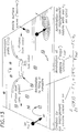
- a starting structure 10 is provided, shown in cross-section in the figure.
- Such starting structure 10 can be supplied as, e.g., a substrate, a thick or thin layer provided on a support such as a substrate, a membrane, or suitable structure.
- a cavity 12 is formed in the structure 10 on a selected surface 14 of the structure and in a region at which an aperture is desired.
- the cavity 12 extends into the bulk of the structure 10 for only a fraction of the structure's thickness, rather than through the entire thickness of the structure, to an opposing surface 18.
- the deepest level, i.e., the bottom 16, of the formed cavity lies at some midpoint in the structure's bulk.
- the geometry of the cavity bottom 16 and the cavity sidewalls 20 are preferably selected to enable controlled formation of a limiting aperture of controlled transverse and longitudinal dimensions in later processing steps. In the example illustrated, a bowl-shaped cavity is employed.
- the structure is progressively thinned from the cavity-free surface 18. As the thinning is continued, a portion 22 of the structure is increasingly removed, shown by dotted lines. This causes the cavity-free surface 18 of the structure to advance toward the bottom 16 of the cavity.
- a limiting aperture 24 is formed which transforms the cavity 12 to an aperture extending through the thickness of the structure. Further thinning of the structure causes the cavity-free surface 18 to intersect upper sidewall locations of the cavity, whereby the limiting aperture 24 takes on that profile of the sidewalls which exists at a given cavity intersection depth.
- the diameter of the limiting aperture 24 increases as thinning is continued, given the bowl shape of the cavity. It is to be recognized, however, that the diameter of the limiting aperture can be made to decrease as thinning is continued, for a corresponding cavity sidewall profile.
- asperities or other distinct profile features or geometry can be provided along the cavity sidewalls for controlling limiting aperture geometry.
- This aperture forming process provides distinct advantages in that it does not rely on direct lithographic techniques for defining final limiting aperture and wall dimensions. As a result, the aperture forming process is not constrained by lithographic resolution limits. The process enables production of a limiting aperture dimension or diameter as small as 1-2 nanometers or less without the need for exotic or expensive processing apparatus.
- this aperture formation process can be carried out on any of a wide range of structures, such as substrates, layers, and films provided on a supporting structure or free-standing as, e.g., membranes.
- Solid state materials in general can be employed as the structural material in which an aperture is formed; microelectronic or semiconductor materials can be particularly effective in enabling efficient processing techniques, as described below.
- the broad classes of inorganic and organic glassy materials such as oxides, glasses, plastics, polymers, and organic films, e.g., PMMA, as well as crystalline materials, such as semiconductors, e.g., silicon and silicon nitride, and metals, as well as other materials can be employed.
- the invention is not limited to a particular structural material or class of structural materials.
- the structural material is selected to meet the criteria of the application specified for the aperture.
- the method is particularly well-suited for enabling formation of apertures in membranes, and for providing the nano-regime control of aperture formation that is required for many membrane applications.
- microelectronic and semiconductor materials and fabrication processes can be advantageously exploited in accordance with the invention to enable cost-effective and efficient manufacturability.
- a starting substrate 30, e.g., a silicon wafer is provided, as shown in Fig. 2A .
- a selected membrane material e.g., silicon nitride
- the thickness of the coating layer 34 is that thickness selected for the membrane to be formed.
- a silicon-rich, low-stress, silicon nitride layer of about 50 nm in thickness is deposited on the silicon wafer by conventional chemical vapor deposition (CVD) processing.
- additional membrane materials e.g., silicon dioxide
- silicon dioxide can be deposited before or after deposition of the silicon nitride layers for mechanical stress control or other consideration.
- the silicon nitride layer can also be further processed, e.g., by ion implantation, to control mechanical membrane stress or adjust electrical or thermal conductivity of the membrane as desired for a given application.
- a layer of photoresist 40 is formed on one of the deposited nitride layers and patterned to define a nitride etch window 38.
- the opposing surface of the wafer is blanket coated with a photoresist layer 40.
- the silicon nitride exposed by the nitride etch window 38 is removed by, e.g., conventional reactive ion etching techniques. This exposes a substrate etch window 42.
- the opposing nitride layer 34 is protected from this etch by the blanket photoresist layer 40, which is removed at the etch completion.
- the silicon wafer is bulk micromachined by a suitable etch procedure, e.g., a conventional anisotropic wet etch process employing KOH.
- a suitable etch procedure e.g., a conventional anisotropic wet etch process employing KOH.
- the bulk wafer etch process employed is characterized by a high selectivity to the wafer material over the membrane material.
- the KOH etch substantially does not attack the silicon nitride layers. Continuation of the etch through the thickness of the wafer thereby produces a self-supporting nitride membrane 36 in a nitride layer 34.
- the nitride membrane forms the bottom of a pyramidal well 39 etched out of the silicon wafer due to the anisotropic, crystallographic-specific nature of the KOH etch.
- the extent of the nitride membrane is thus determined by the thickness and crystallographic orientation of the starting silicon wafer. As will be recognized, the membrane dimensions can therefore be controlled as-desired.
- the remaining layer 32 of silicon nitride opposite the membrane layer can then removed if desired by, e.g., conventional reactive ion etching, and then a layer of silicon dioxide 41 is optionally grown on the exposed silicon surfaces, if electrical insulation of the silicon wafer is desired for a given application.
- Conventional wet or thermal oxide growth can be preferred over a CVD oxide layer such that oxide is only formed on the silicon surfaces in the manner illustrated.
- a composite membrane is desired, e.g., for mechanical stress control, then a CVD or other deposition process can be employed to produce an oxide layer on both the silicon wafer and the lower silicon nitride membrane surfaces, or on the nitride membrane surface alone.
- a cavity is formed in a selected surface of the membrane.
- an etching process as illustrated, a layer of resist 42 is formed on the lower membrane surface, i.e., the membrane surface opposite that in the pyramidal wafer well.
- the resist is then patterned to define the cavity to be formed in the membrane.
- This choice of surface for the cavity can be preferable for enabling a selected lithography technique on a flat surface; it can be difficult to effectively pattern a layer of photoresist provided on the membrane surface at the bottom of the silicon pyramidal well.
- the cavity can be formed on such a surface with lithographic techniques specific to such a configuration.
- the present application contemplates the use of photolithography, electron beam lithography, and other suitable lithographic processes for defining the cavity pattern. It is to be recognized that the selected lithographic process is preferably suited to the dimensions of the cavity; e.g., electron beam lithography can be preferred over conventional photolithography for cavities having submicron dimensions.
- the sidewall profile of the cavity to be formed in the membrane can be specified to produce a selected limiting aperture geometry.
- the lithographic step defining the cavity, as well as the nature of the cavity etch process itself, can also be employed to define the cavity sidewall profile.
- the selected lithographic cavity pattern is continuous, e.g., as a circle, and a relatively isotropic etch process, e.g., an isotropic reactive ion etch process, is carried out to form a bowl-shaped cavity 12 in the nitride membrane 36, as shown in Fig. 2G .
- An isotropic reactive ion etch process inherently forms the bowl shape extending from a circular photolithographic pattern.
- the present application contemplates the use of substantially any cavity pattern for achieving a desired cavity geometry.
- Square, rectangle, hexagonal, or other pattern, symmetric or asymmetric can be employed. Due to the batch nature of lithographic processes and other microfabrication processes employed in the aperture forming method, arrays of cavities, of varying extent and geometry, can be defined in a single structure such as the membrane illustrated. Because the aperture formation process relies on structural thinning, rather than lithography, to define the final limiting aperture geometry, the largest lateral dimension of the cavity can be much greater than the desired limiting aperture extent; in general, the largest cavity pattern dimension can be two or more orders of magnitude larger than a selected limiting aperture diameter.
- the cavity pattern extent is correspondingly selected to produce a desired extent at the cavity bottom, and to produce a range of cavity expanses between the cavity bottom and the material surface.
- Any suitable cavity etch process can be employed, including, e.g., plasma etching, focused reactive ion etching, focused ion beam etching, wet chemical etching, or other selected technique. Whatever etch process is selected, it is to be controlled to enable termination of the etch at a cavity bottom located at some distance within the membrane thickness or other structure in which the cavity is formed, i.e., at a point between the surfaces of the structure. For etch processes that are fully characterized for the structural material being employed, this can be accomplished by a timed etch; conventional diagnostic techniques otherwise can be employed in the conventional manner to produce a cavity bottom at a selected location in a membrane other structure.
- etch processes can be employed as-necessary for cavity formation in a given material or composite of materials. For example, where a composite membrane is formed of silicon nitride and silicon dioxide layers, the chemistry of a selected cavity etch, such as a plasma etch, can be adjusted over the course of the etch based on the material to be etched at a given time in formation of the cavity. Similarly, a combination of etch processes can be employed to alter the cavity sidewall profile as a function of cavity depth.
- a combination of isotropic and anisotropic wet etches can be employed to produce selected curvature and slant of cavity sidewalls formed in a nitride or silicon layer or membrane.
- a combination etch such as this enables the formation of asperities or other distinct features to be located at the limiting aperture.
- thinning of the structure is then carried out on the structure surface opposite that in which the cavity was formed, employing an appropriate procedure to open a limiting aperture in the structure.
- the present application contemplates a wide range of thinning processes and is not limited to a particular thinning technique; all that is required is the ability to etch back the structure from a surface opposing that in which the cavity was formed.
- a particularly well-suited thinning process is ion beam sputtering.
- a beam of ions is directed to the structure surface to be thinned to sputter etch away material from that surface.
- typical ion beam sputtering processes at relatively low beam energies, e.g., in the range of keV, for every incident ion, on average, a single atom of material is ejected from the sputtering target; sputtering may thus be considered as an atomic-scale version of "sand blasting.”
- a silicon nitride membrane such sputter etching results in the removal of about one atomic layer of silicon nitride from the membrane per second for incident ion fluxes between about 10 14 -10 15 ions/cm 2 /sec.
- the present application contemplates a wide range of additional thinning processes, including ion beam assisted etching, ion beam induced etching, electron beam etching or assisted etching, plasma and reactive ion etching, wet etching such as electrochemical etching, chemomechanical polishing, and other fabrication and manufacturing processes that enable controlled thinning of a structure to intersect a cavity on a surface opposite that being thinned.
- These aperture formation processes can be advantageous for many applications because during the thinning etch, the etch species, e.g., a sputtering ion beam or reactive plasma environment, need not be focused on a particular location of the structure surface being thinned.
- a blanket exposure of the structure surface can be employed to thin the entire extent of the structure. All that is required is that the structure surface including the cavity be isolated, i.e., shielded, from the etch species attacking the opposing surface. This results in nano-regime precision in feature formation without the requirement of nano-regime control of the etch apparatus and species.
- the inventors herein have discovered that highly precise aperture formation can be accomplished by implementing a feedback mechanism during the thinning process.
- This feedback mechanism is based on detection of a physical species provided during the thinning etch in a manner that is indicative of the physical dimensions of a feature, e.g., an aperture, that is being produced by the etch.
- Such feedback enables real time control of the aperture formation process, whereby a precise and prespecified aperture diameter can be reliably and reproducibly formed.
- this feedback mechanism can in general enable precise sculpting of nanometric features and nanostructures, and finds wide application for micro- and nano-systems.
- etch species such as a beam of sputtering ions
- ions from the beam are at that point in time enabled to pass through the aperture.
- the number of ions passing through the aperture per unit time is proportionally related to the increasing diameter of the aperture as the thinning etch continues.
- Detection and quantification, e.g., by counting, of the rate and/or number of ions passing through the aperture thereby is indicative of the aperture diameter at any given time during the etch.
- a selected aperture diameter can be prespecified based on a rate and/or number of ions expected to pass through the aperture before the selected diameter is produced.
- a first passage of ions through a newly-formed limiting aperture can be detected, and the number of ions passing through the aperture as its limiting aperture dimension enlarges can be individually detected and quantified.
- a controlling signal can be sent to the sputtering ion beam controller to terminate the etch process at the desired aperture dimension.
- detection of a physical species can be carried even prior to the time at which an aperture is formed.
- the level of X-rays produced by the ion beam gun that are detected as passing through the structure being thinned can be expected to increase as the thickness of the structure decreases. Detection of ions similarly can be made even prior to aperture opening. This enables control of the process even prior to the final opening of the aperture.
- the system includes an ion gun 52, e.g., an ion gun capable of producing an ion beam with an energy range and diameter suitable for a given application. In general, an energy between about .05 eV and about several hundred KeV and a beam diameter between about a few nanometers to spatially very broad beams can be employed.
- a vacuum etch chamber 55 is provided in which the etch process can be carried out.
- the etch chamber pressure is well-controlled such that etch environment pressures of less than about 10 -8 Torr (1 Torr corresponds to approximately 133 Pa) can be maintained during the etch process.
- a load-lock sample entry system that is vented with, e.g., dry nitrogen, to minimize exposure of the etch chamber to contaminants.
- a turbomolecular pump 57 is provided for pressure control and maintenance.
- a mass spectrometer can be provided for monitor and analysis of the etch environment species.
- a structure holder 54 is provided for supporting a structure 10 in which an aperture is to be formed, e.g., employing clips to maintain the position of the structure.
- the holder 54 is thermally conductive and provides structure temperature control, e.g., by a liquid heat exchange loop, employing a thermocouple positioned on the holder or on the structure itself.
- the holder also be electrically conductive to enable voltage charge control of the structure and to enable monitor of incident ion beam current.
- the holder includes a central aperture 56 corresponding to the location at which an aperture is to be formed in the structure 10.
- an electron flood gun 59 can be included in the arrangement to direct a beam of electrons at the structure being etched during the etch process.
- positive electrical surface charge can accumulate on the structure due to positively-charged ion beam irradiation. Electron beam irradiation of the structure can be carried out to neutralize this surface charge, if necessary for a given application.
- the stream of a species traversing the etched aperture is to be detected and quantified in the manner described below. If no such feedback control is desired for a given application, then no additional apparatus is necessary, and the sputtering can be carried out in a conventional sputtering chamber under conditions selected for a given etch.
- species detection and quantification systems can be included to provide a desired degree of feedback control.
- ion focusing optics 60 can be provided for focusing the ions once they traverse the aperture, to facilitate ion detection by a detector that is relatively distant from the structure aperture through which the ions traversed.
- X-Y deflection optics and Einzel lenses can be employed in conventional configurations to produce a desired focusing of the ions.
- optics design software can be employed to produce a customized focusing configuration for a given detection arrangement.
- focusing configuration may not be required for configurations where the ion detection system is relatively near to the holder aperture. If focusing optics are employed, it can be preferred to mount such, e.g., behind a stainless steel plate supported by an upper flange of the etch chamber 55, to provide mechanical stability to the optics as well as shield the ion detector, described below, from stray ions from the ion gun.
- the focusing configuration preferably directs the output ion beam to an ion energy analyzer 62 for filtering the beam for the selected species to be detected and quantified by, e.g., counting.
- the ion beam sputtering process will include and produce a wide range of physical species and radiation, including, e.g., sputtered silicon nitride atoms, etch species scattering in the etch chamber, and X-rays emanating from the ion gun.
- the species to be detected is preferably filtered out from the produced radiation, produced etch species, and background radiation.
- Such background can be minimized by, e.g., isolating the ion beam gun, the structure to be etched, and the downstream optics from further downstream components such as detectors, as described below, by an electrostatic energy filter or other suitable filter.
- it can be preferable to maintain the ion beam gun, structure, and optics at reduced temperature conditions in a suitable vessel, as shown in Fig. 3B , whereby thermal effects can be controlled.
- a cooling configuration is also useful to maximize cleanliness of the etch and beam detection environment and to control structure temperature. It can also be advantageous to maintain the structure at an elevated temperature to influence materials modification phenomena during ion irradiation.
- an ion energy analyzer 62 or other species-specific filtering system is advantageous in that it enables redirection of a species to be detected out of the line of sight of the sputtering trajectory.
- the species detection location can then be distant and out of line from bombardment by background and produced radiation such as X-rays.
- the electrostatic energy analyzer employed produces a 60°- 90° bend in the trajectory of the ion species to be detected, whereby that species is separated from the other species and radiation coming from the etched structure. If the detection resolution and speed desired for a given etch process do not require a low background noise environment, then the ion energy analyzer is not required for many applications.
- the filtered species of interest output from the electrostatic energy analyzer is directed to a detector 64.
- a detector 64 For the detection of an electrically charged ion species, it can be preferable to employ a high-resolution, single ion detector, e.g., a Channeltron 4860 detector from Gallileo Electro-Optics of Sturbridge, MA. Such a detector can be configured to produce one electrical output pulse per detected ion.
- Such single ion detection and associated counting can be preferred for many applications to enable nanometric-scale precision in production of a solid state feature such as an aperture. While a typical sputtering beam current density is about 10 ions/nm 2 /sec, etching of a nanometer-range aperture requires counting of the passage of no more than about 10-20 ions through the aperture.
- a single ion detection and counting system is preferred to reproducibly implement nano-regime control of feature production. If the features to be produced for a given application do not require nanometric dimensional control, then a more coarse detection mechanism can be employed. It can be preferred for many applications to shield the ion energy analyzer and detector from potential electrical noise sources by encasing such in, e.g., an aluminum can that includes an aperture through which the beam can enter. In this scenario, the ion beam is preferably aligned with a sample to be processed and the encased detector, by adjusting beam focus voltages so as to maximize the transmitted ion count rate through a control sample containing a hole.
- a fast pulse amplifier 66 can be employed to modify the electrical output of the detector to facilitate an ion counting process.
- a suitable pulse preamplifier can be constructed in a conventional manner or a suitable commercial system, e.g., the VT120 Fast Preamp from EG&G Ortec of Oak Ridge, TN, can be employed.
- the pulse amplifier 66 can be configured to amplify the pulse voltage to about 1 V.
- This amplified detection pulse is directed to a counting system, e.g., a universal counter such as the HF53131A by Hewlett Packard, for producing an electrical signal indicative of the number of detected ions. It is recognized that detection pulse amplification may not be required for a given pulse counter configuration, and that the pulse amplification, if implemented, is preferably controlled based on requirements of the counting system.
- the electrical output of the pulse counter 68 is directed to a controller 70 that implements, e.g., monitor and control software for enabling an operator to monitor the thinning etch process in real time and for producing an ion gun control signal.
- the controller is implemented in software employing, e.g., Labview, from National Instruments, of Austin TX. Whatever controller implementation is selected, it preferably provides ion beam control signals based on the ion feedback.
- the controller can be implemented to initiate ion beam sputtering of the structure for a specified time interval and to configure the counter to count the number of ions received at the detector during the specified time interval.
- the number of ions counted is determined by the controller and the extent of the aperture can at that point be calculated based on this ion count and the known ion flux.
- the number of ions counted during the interval is then employed by the controller to determine if a further interval of ion beam sputtering is to be initiated to continue etch of the structure.
- a computer system including monitor, memory, and associated input/output and printing systems is provided for enabling visual monitoring and recording of the etch process progression. Display of the ion count rate and aperture extent over time, and storage of count rate and other system values can be preferable for many applications.
- the output of the controller 70 is directed to an ion gun control system 72 for controlling the sputtering etch itself.
- ion gun feedback control is effected by control of the ion gun's X-Y deflection plates to deflect the ion beam away from the structure 10 at the time when the desired aperture dimension is produced. This can be a preferable control technique because of the rapid speed at which the beam can be deflected, typically in much less than a millisecond.
- an electrostatic grid can be located between the gun and the structure holder. In this scenario, the grid is energized in response to an ion beam termination control signal to return the beam back toward the ion gun.
- the accelerating electron impact voltage of the ion gun can be controlled in response to an ion beam termination control signal to terminate production of the ion beam.
- a feedback calibration curve can be produced for a given ion beam species, structure material, and aperture geometry to be produced.
- Such a calibration curve enables specification of the relationship between ion count number and/or rate and limiting aperture dimension, and can be established empirically, to specify for a particular structural material and thickness a relation between number of measured counts per time and actual limiting aperture dimension.
- an extrapolated calibration curve can be produced based on a few measurements. To produce each such measurement, a thinning etch is carried out for a prescribed duration, during which an ion count is made and at the end of which an aperture dimension is physically measured by, e.g., transmission electron microscopy. Multiple etch durations and dimensional measurements can be carried out on a single aperture as that aperture is increased from etch to etch. A calibration curve can then be produced based on the ion count and aperture measurements and extrapolated to lower and higher ion counts. With such a calibration curve in hand, the controller system of the feedback configuration can be programmed to direct a controlling etch termination signal to the ion gun when the prescribed ion count corresponding to a desired aperture dimension is reached.
- etch environment temperature and pressure, mechanical stress and temperature of the structure being etched, and feature dimensions and structural aspects can influence the relationship between detected ion count rate and physical feature dimensions.
- the residual mechanical stress in a silicon nitride membrane can impact its etch characteristics.
- the density of apertures in an array to be formed, the aperture proximity to each other, and other aspects can impact etch characteristics.
- the calibration curve preferably is produced with consideration for various physical and etch environment parameters that can impact etch characteristics.
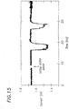
- FIG. 4A is an electron micrograph of the cavity formed in the membrane.
- the membrane surface opposite that including the cavity was exposed to an argon ion beam etch at an energy of about 3 KeV, and a flux of about 3 Ar + sec/nm 2 .
- the ion beam diameter was about 200 ⁇ m and the membrane temperature during the etch was maintained at about -120°C.
- the ion beam was directed toward the membrane for 1 sec during each 5 sec interval. During the etch process, ion detection and counting was carried out.
- Fig. 4B is an electron micrograph of the membrane cavity including a 10 nm limiting aperture formed by thinning of the membrane.
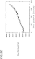
- Fig. 4C is a plot of argon ion count/second as a function of sputtering time. This plot includes that time when the ion beam was directed to the membrane, not when the beam was deflected away from the membrane. As indicated by the plot, the number of counted ions/sec was substantially zero until at point in time, at 25 sec, when the limiting aperture was opened. Then as the limiting aperture diameter increased, the ion counts correspondingly increased. This enables control of the aperture formation process.
- etching of the aperture was enabled by detection and counting of electrically charged ions that traversed the aperture once it was opened.
- the species operating as an etchant also operated as the species to be detected. This dual role of the ion beam is not in general required.
- the etchant species is selected and operates distinctly from the detection species. For many applications, such a decoupling of the etchant and detection species can be advantageous in enabling a broader range of candidate species for both etchant and detection species.
- an atom beam etch species if the beam is electrically neutral rather than electrically charged, detection of the atoms can be difficult.
- a distinct non-etching detection species such as an electron beam can in this case advantageously be employed for controlling formation of a prespecified aperture diameter.
- Such a scenario can be preferable where the structure being etched may become electrically charged by the impinging sputter beam, thereby warranting the use of an electrically neutral beam.
- an electrically charged detection species for facilitating beam bending, filtering, and detection and counting with conventional techniques.
- Electrically neutral detection species can be employed, however, when such is optimal for a given application. For example, laser fluorescence of electrically neutral transmitted atoms can be employed for detecting and counting control functions.
- a separate detection species is preferably one that can be directed in some manner toward a feature being produced and whose movement in the vicinity of the feature is indicative of changing dimensions of the feature. This enables detection of the species in a manner that is indicative of changes in the feature's dimensions. For example, in the case of formation of a membrane aperture, direction of an electron beam toward the membrane, such that electrons traverse the membrane aperture once it is formed, enables counting of electrons in the manner of ion counting described above.
- the method does not require the use of a single detection species; more than one detection species can be employed. For example, X-rays produced by the ion gun can be monitored as the structure thins to predict and indicate a the time of a further aperture formation event. Thereafter, ions, electrons, or other species can be employed to monitor changes in aperture diameter. Neutral species and other species suited to a given application can similarly be employed together to provide precise detection and feedback mechanisms.
- the method does not require that the detection species be directed orthogonally to the plane of a feature being produced.
- electron beam diffraction detection and the diffraction patterns produced by a material can be employed as a feedback mechanism.
- detection of the electron beam diffraction pattern characteristic of the lower layer can be employed as the feedback mechanism.
- the electron beam makes a glancing angle with the material.
- diffraction can be detected as a function of the aperture diameter by diffraction rings indicative of changes in aperture periphery.
- the diffraction feedback mechanism here occurs at the aperture periphery rather than as a trajectory through the aperture.
- an electron beam can be directed parallel to the upper structure surface being thinned in formation of an aperture, whereby the withdrawal of surface material is indicated by an increase in electron count in a direction parallel to that surface.
- atoms in a meta-stable state can be directed toward a feature being formed and detected once past the feature.
- Such meta-stable atoms e.g., excited states of helium or argon, are electrically neutral and do not decay until hitting a solid surface, at which time an electron is liberated and can be detected and counted.
- Whatever detection species is selected it preferably is one that can be detected and counted on a time scale that is commensurate with the desired dimensional scale of control in the feature being produced. For example, where nanometric feature dimensions are of importance, microsecond detection and counting processes are preferable to enable high sensitivity and resolution in the feedback mechanism. Less strict sensitivity and resolution requirements need be placed on detection species for micro- and macro-scale feature control.
- the present application contemplates application of physical species detection and counting for feedback control in a wide range of fabrication processes.
- Many fabrication processes that are conventionally carried out in open loop fashion, i.e., without feedback control, can be adapted to enable nanoscale dimensional feature control with the incorporation of the highly sensitive and precise feedback mechanisms.
- reactive ion etching in a plasma rather than sputter etching, can be employed to thin a structure surface in formation of a limiting aperture.
- the structure surface including a cavity is isolated from the plasma environment by a suitable fixture.
- the opposing structure surface is fully exposed to the plasma environment.
- ions traversing the aperture are detected by, e.g., a channeltron positioned on the isolated side of the structure. Accordingly, in the manner of the ion sputtering etch described above, feedback control can be imposed on the plasma etch process based on the detection and counting of plasma ions traversing the aperture.
- physical detection and feedback control can be imposed on a wet etch process employed to produce a feature.
- electrodes can be provided near to the cavity formed in the structure.
- the structure surface opposite the cavity is exposed to a wet etch environment, e.g., an electrochemical environment, and the structural surface which includes the cavity is isolated from the etch environment.
- a wet etch environment e.g., an electrochemical environment
- ions in the liquid that traverses the aperture can be detected and counted at the cavity-side electrodes. This enables feedback control for terminating the electrical stimulus of the etch at a time when the desired aperture dimension is attained.
- the present application contemplates implementation of physical species detection and feedback process control for enabling fabrication of a wide range of structural, solid state features.
- the feedback mechanism is not limited to the aperture formation process described above.
- an aperture, slit, trench, hole, or gap between two feature edges can be precisely formed, by any of a wide range of processes, in a precise and controllable manner with the feedback mechanisms.
- a membrane aperture formation process employing, e.g., focused ion beam or plasma etching techniques where a hole is formed directly through the thickness of the membrane from one surface to the other of the membrane
- feedback can be employed to control and monitor the formation.
- the Present application contemplates a membrane aperture formation process where a cavity is formed in one surface of the membrane and then that membrane surface, including the cavity, is exposed to, e.g., an ion sputtering etch. Because the thickness of the membrane between the cavity bottom and the opposing surface is much less than at other membrane regions, such etching opens a limiting aperture at the base of the cavity before completely etching away other regions of the membrane.
- the feedback mechanisms enable precise control and monitoring of this process.
- a silicon nitride membrane of about 50 nm in thickness was produced in the manner of Figs. 2A-2E .
- An aperture was formed through the entire thickness of the membrane by reactive ion etch. This resulted in a 37 nm-wide aperture, an electron micrograph of which is shown in Fig. 5A .
- the membrane and aperture were then exposed to an argon ion beam at a flux of about 1.7 Ar + /nm 2 /sec and an energy of about 3 KeV.
- the ion beam was directed toward and away from the membrane to sputter for 1 second during each 5 second interval.
- the membrane was maintained at a temperature of about -102°C during the ion beam exposure.
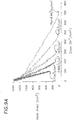
- Fig. 5B is an electron micrograph of the 58 nm-wide aperture that resulted from 180 seconds of sputtering.
- Fig. 5C is a plot of counted ions/sec as a function of time. A generally linear relationship between ion counts as a function of time is demonstrated.
- the process being controlled by feedback be a subtractive process as in Example 2; additive processes can also be controlled by the feedback techniques of the invention.
- an aperture, trench, or hole of a given dimension can be diminished or narrowed, by a suitable process, during which the physical species detection and feedback process control is imposed to control the diminishing process.
- Sintering, heating, material deposition, material growth, and other suitable processes are contemplated as being controllable by the feedback mechanism.
- oxidation, swelling, material flow and transport as described in detail below, condensation, evaporation, electroplating, ion- or electron-assisted deposition or growth, and other such additive processes can be controlled.
- the only requirement of the process to be controlled, whether additive or subtractive, is that the process accommodate the introduction of some detection species near to the structural feature being processed in a manner that enables detection of that species as an indicator of changing feature dimensions.
- the features can be produced in a membrane, in a layer or layers provided on a support structure, or in a structure itself, e.g., a silicon wafer.
- the advantages of the control processes of the invention can be most fully exploited and realized in the formation of nanometric scale feature dimensions and dimensional tolerances.
- This capability can be particularly advantageous for producing a field of nanometric features, e.g., in formation of a lithographic mask plate.
- a starting membrane can be processed with selected geometries to ultimately form wires, pads, and other mask plate geometries by additive or subtractive processes. This enables precise formation of the mask plate features in an efficient and effective process.
- the invention provides an additional process control feedback technique and corresponding apparatus for controlling fabrication processes in real time based on a feedback parameter indicative of the process results.
- this feedback technique a bias voltage is applied across the gap of an electrically conducting feature or features being modified by a fabrication process, as the process proceeds, and the electron tunneling current across the gap that results from the applied voltage bias is monitored as the process proceeds.
- the monitored electron tunneling current enables a very high resolution, real time measurement of changes in the gap dimensions because the gap extent is directly related to the tunneling current for a given applied voltage bias.
- a measurement of tunneling current is related to a corresponding gap dimension based on the tunneling regime at which the gap is biased.
- a first of two tunneling regimes considered in accordance with the invention, the Fowler-Nordheim tunneling regime, is characterized by relatively large gaps, i.e., gap extents greater than about 1-2 nm, and applied voltage biases that are greater than the work function of the material in which the gap exists.
- the second tunneling regime to be considered for correlating measured tunneling current with gap dimension corresponds to relatively smaller gap extents, i.e., less than about 1-2 nm, and applied voltage biases less than the work function characteristic of the material in which a gap is provided.
- one of the expressions above can be employed to make a correspondence between measured tunneling current and corresponding gap dimension as a process proceeds.
- it can be preferred to preliminarily calibrate the expressions for a given material and given process conditions, based on known gap dimensions so that real time correspondence can be made easily, i.e., so that each tunneling current measurement can be correlated in real time to a previously determined, known gap extent. This enables control of a fabrication process in real time to produce a selected gap extent based on in situ tunneling current measurements as a process proceeds.
- a tunneling current feedback control loop can be implemented, in one example, with a computer 70 having a computer control program, e.g., the Labview program described above, configured for a selected fabrication process.
- the computer control is specified to generate a bias voltage selected for a given process and a gap extent of interest, e.g., based on the selected one of the tunneling current-voltage expressions given above.
- Application of the bias voltage is to be made across a gap in an electrically conducting feature or features of a sample to be processed 10.
- the digital voltage output specification from the computer is first converted to an analog voltage signal by a digital-to-analog converter (DAC) 80.
- the analog voltage signal can be amplified by a voltage amplifier 82 if the DAC limits the bias voltage below that required for a given application.
- the analog voltage is then applied across a gap in an electrically conducting feature or features being processed.
- Electrical contact can be made to the electrically conducting features in any suitable and convenient fashion that enables a robust electrical connection as the sample is being processed.
- electrical contact is made to a sample as the sample is exposed to an ion beam 58 in the manner described above, but this specific processing is not required; as explained above, the feedback techniques of the invention are applicable to a wide range of fabrication processes. Whatever process is carried out, the only requirement is that a robust electrical connection be provided for applying a bias voltage across a gap of interest during the processing.
- the electrically conducting material at the location of the gap be itself patterned or connected to a material that is patterned as contact pads of a macroscopic scale, e.g., at least about 100 ⁇ m square, such that conventional wire bonding, spring clips, or other selected connection technique can be employed.
- a current amplifier 84 that preferably is characterized by a high acquisition speed and a high gain factor, if desirable for a given application.
- the measured current is digitized by an analog-to-digital converter (ADC) 86 and delivered to the computer 70.
- ADC analog-to-digital converter
- the computer is programmed with a prespecified threshold tunneling current against which the measured tunneling current is compared as the process proceeds.
- the computer directs an ion gun controller 72 to control the ion gun 52, e.g., to extinguish exposure of the sample to the ion beam.
- the fabrication process is directly controlled in real time based on in situ monitoring of the tunneling current across a gap or gaps in a sample as the sample is processed.
- the programmed threshold tunneling current can be set in any suitable manner. For example, based on the Fowler-Nordheim expression given above, the tunneling current corresponding to a desired gap size can be determined for a given material and voltage bias application. With the tunneling current thusly determined, the computer can be programmed with that tunneling current value for comparison with tunneling current measurements as the process proceeds.
- the invention contemplates a wide range of alternatives for providing a tunneling current threshold; such can be determined, e.g., in real time; a programmed look-up table can be employed, or other technique can be implemented for enabling feedback control of a process based on tunneling current measurements.
- This feedback control technique can be extended to any fabrication process that can accommodate application of a voltage across and measurement of tunneling current across a gap in an electrically conducting material.
- No specific arrangement is needed for the monitored gap; all that is required is a gap the extent of which will increase or decrease in a manner that relates to a fabrication process to be controlled.
- the extent of the gap can be made larger or smaller by the fabrication process to be controlled, and/or the gap can be nonexistent at the start of the process or be closed during the process. It is correspondingly not required that a tunneling current measurement be possible at all times during a fabrication process under control. If the process is initiated in a material without a gap and results in the formation of such, tunneling current measurements can be made once the gap appears.
- tunneling current measurements can be made during the interval of the process when a gap exists.
- tunneling measurements may be possible only during an interval of a fabrication cycle when the gap extent is sufficiently small to enable tunneling.
- a tunneling current measurement can be made at selected points in time during a fabrication process rather than continuously; as described in detail below, because the tunneling current measurement can under some circumstances itself impact the process; brief, intermittent tunneling measurements can therefore be preferred for some applications.
- the ion counting feedback technique described previously can be employed in concert with the tunneling current measurement feedback technique.
- the ion counting feedback can be employed for control of processing larger features that are, e.g., tens of nanometers or more in extent, and the tunneling current measurement feedback control then employed for fine tuning the larger features or producing finer features that are, e.g., tens of nanometers or less in extent.
- the two feedback control techniques can be employed simultaneously, e.g., for controlling fabrication of electrically conducting and electrically insulating features, or employed sequentially in any order.
- the tunneling current measurement technique of the invention is particularly advantageous for enabling real time fine tuning of a feature, such as a nanoelectrode gap, in a precise and reproducible manner, and therefore for many applications can be advantageously employed after relatively gross dimensional control by the ion counting feedback technique.
- the inventors herein have discovered that the conditions of interaction between an ion beam and a solid can be controlled for manipulating nanoscale feature dimensions in solid state materials.
- These controlled ion beam interaction techniques enable solid state material topology to be adjusted, rather than necessarily removed.
- solid state material can be caused to transform such that feature edge locations are precisely and controllably produced and/or modified by atomic transport mechanisms that are locally additive or subtractive.
- a limiting aperture 24 in a structure 10 is caused to be adjusted from a first diameter, D 1 , to a smaller diameter, D 2 or D 3 .
- the starting aperture is formed in a selected structure in any suitable fashion, e.g., by the methods described above and shown in Figs. 1A-1D and Figs. 2A-2G , in, e.g., a membrane, layer, substrate, or other structure.
- the structure surface 18 in which the limiting aperture was formed is then exposed to ion beam irradiation, employing, e.g., the system described above and illustrated in Figs. 3A-3B .
- the inventors have discovered the unexpected result that the material is added to the periphery, or boundary, of the limiting aperture 24 exposed to the irradiation, causing the diameter of the limiting aperture to decrease.
- This condition can be predictably and precisely imposed by enforcing structure temperature, ion flux rate, and ion energy conditions conducive to material addition at the aperture rim.
- the ion beam irradiation is generally considered to be a sputtering/material removal process, it is particularly unexpected that this material movement and addition condition can effectively progress, even in the presence of the atomic sputtering erosion, to result in a change in the physical dimensions of a feature.
- FIG. 7A is an electron micrograph of the 95 nm-wide aperture that resulted from the etch.
- the membrane and its aperture were then exposed to an argon ion beam flux at an energy of about 3 KeV, and a flux of about 47 Ar + /sec/nm 2 .
- the membrane was maintained at a temperature of about 20°C during ion flux exposure.
- the ion beam was directed to the membrane for 250 ms for each 1 sec time interval.
- Fig. 7B is an electron micrograph of the membrane after exposure to the argon ion beam reduced the aperture diameter to about 3 nm.
- Fig. 7C is a plot of counted argon ions/sec as a function of time. A generally linear count rate is indicated for midpoints in the process.
- the mechanisms underlying the ability of an ion beam to cause material build up at an ion-irradiated aperture rim may be related to atomic transport through the bulk of the structure; ion-induced changes in viscosity, electronic surface charge, mechanical stress generation, and lateral swelling of the structure; and/or atomic surface transport caused by ion-induced surface atom excitation or supersaturation of mobile adsorbed ionic species on the structure surface.
- the ion penetration depth is much less than the structure thickness, resulting in a domination of surface transport processes.
- the method does not require a specific material transformation mechanism, but rather, provides distinguishing process control parameters that impose predictable material transformation results.
- the temperature of the structure being exposed to the ion beam irradiation directly impacts the ability to impose material movement and the rate at which material moves. It is found that for a specific structural material, there is a characteristic temperature above which material of the structure is found to move, resulting in an adjustment, or change, in feature dimensions and below which material is instead removed by sputtering from the structure. For given ion beam energy and flux conditions, control between material removal and dimensional feature adjustment can therefore be imposed by structural temperature control.
- Fig. 8 there is plotted the ion counts/second detected by an ion sputtering system like that of Fig. 3A as a function of time for a 500 nm-thick silicon nitride membrane in which was initially fabricated a square aperture of about 72 nm in length.
- the membrane was fabricated based on the process shown in Figs. 2A-2F and the aperture was fabricated by a focussed ion beam directed at the membrane to form an aperture that extended completely through the membrane.
- Each region of the graph indicates the temperature at which the membrane was maintained during bombardment by an argon ion beam.
- the beam flux was 14 Ar + /sec/nm 2 and the beam energy was 3 KeV.
- the on/off duty cycle of the ion beam being directed toward the membrane was such that the beam was directed to the membrane for 200 msec during each 1 sec interval.
- the plotted data also indicate that within the regime for imposing material movement and addition, the rate of material transport in altering feature topology is temperature dependent. At relatively higher temperatures, the transport process proceeds more rapidly than at relatively lower temperatures. Knowledge of this temperature-dependent transport rate enables precise process control and characterization.
- nitride membranes Five silicon nitride membranes of about 500 nm were fabricated in the manner of the process outlined in Figs. 2A-E . Apertures each of about 1400 nm 2 in area were produced in the membranes by focused ion beam etching. The membranes were then exposed to an argon ion beam at an energy of about 3 KeV for various total doses at five ion beam fluxes. Each membrane was maintained at a temperature of about 22°C during the ion beam exposure. Each ion beam exposure was controlled to sputter for 200 msec during each 1 second interval.
- Figs. 9A-9B there is plotted the area of the apertures in nm 2 as a function of total argon ion beam dose, in ions/nm 2 , for five different argon ion beam fluxes, and the aperture area decrease per dose, as a function of argon ion beam flux, respectively. From the plotted data, it is indicated that as a function of total argon ion beam dose, the aperture shrinks more rapidly at low incident fluxes relative to higher incident fluxes. In other words, the lower the flux, the less dose is required to shrink an aperture.
- the strong nonlinearity indicates that the amount of material mass transport produced by the ion beam irradiation per incident ion may be suppressed at high incident fluxes. This characterization enables operation at a selected mass transport rate.
- the present application contemplates empirical analysis of flux dependence for a selected material, to enable precise control of the material movement.
- a 50 nm-thick layer of silicon nitride was deposited by low pressure chemical vapor deposition on a silicon wafers.
- the silicon nitride layer was patterned by electron beam lithography to produce trenches of about 50 nm in width through the entire thickness of the silicon nitride layer. The bottom of each trench thereby exposed the underlying silicon surface.
- Fig. 10A is a scanning electron micrograph of the trenched silicon nitride layer on the silicon wafer.
- the trenched silicon nitride layer was exposed to an argon ion beam at an energy of about 3 KeV and a flux of about 20 Ar + /nm 2 /sec, where the ion beam was sputtering for 0.5 seconds for each 2 second interval.
- the silicon wafer was maintained at a temperature of about 20° C during the ion beam exposure.
- Fig. 10B is a scanning electron micrograph of the trenched silicon nitride layer after about 200 seconds of sputtering. Note that silicon nitride material has been moved to the trenches, whereby the trenches have been partially filled in. This indicates that for the process conditions here employed, material is transported from the silicon nitride layer to the trenches.
- a second 50 nm-thick trenched silicon nitride layer like the one just described was exposed to an argon ion beam at an energy of about 3 KeV and an ion flux of about 30 Ar + /nm 2 /sec, with the ion beam sputtering for one second during each two second interval, for a total sputtering time of about 300 seconds.
- the silicon wafer was maintained at a temperature of about -100° C during the ion beam exposure.
- Fig. 10C is a scanning electron micrograph of the trenched silicon nitride layer.
- the silicon nitride material at the top of the trenches has been etched away, as indicated by the rounding of the trench edges, but the bottom of the trenches are not at all filled in.
- This example demonstrates the temperature control that can be imposed to predictably produce material transport and feature adjustment or material removal by sputtering as desired for a given application.
- the energy of the ion beam can impact the nature of material transport. Specifically, for a given structural material and temperature, a given ion beam current density, and a given time structure of the ion beam exposure, as discussed below, there exists an ion beam energy above which material transport is effectively induced in the manner described above and below which sputtering in the conventional manner occurs.
- This juncture between the two distinct operational regimes can be empirically determined for a given material and ion beam exposure system, and can be employed as an important control technique for precisely enabling and disabling the material transport processes.
- the time structure of the ion flux exposure i.e., the sequence of intervals in which the ion beam is controlled to enable interaction with a material and then controlled to not interact with the material, impacts the nature of material transport and dimensional feature change.
- the imposition of an on/off duty cycle on the ion flux is found to impact the ability to cause material movement and corresponding dimensional feature change.
- a 500 nm-thick silicon nitride membrane was produced in the manner of the process outlined in Figs. 2A-E .
- a 95 nm-wide aperture was formed through the entire thickness of the membrane by focused ion beam etch.
- the membrane and aperture were then exposed to an argon ion beam at an energy of about 3 KeV and a flux of about 14 Ar + /sec/nm 2 .
- the membrane was maintained at a temperature of about 16 °C during the ion beam exposure. During the exposure, the amount of time that the ion beam was directed to the membrane was varied.
- Fig. 11A is a plot of argon ions counted/second as a function of sputtered time. The plot indicates that the 400 msec/1 second interval and the 600 msec/1 second interval time structures increased the aperture diameter, while all other time structures decreased the aperture diameter. This demonstrates that at about room temperature, control between material transport processes and sputtering processes can be achieved by control of the ion beam exposure time structure.
- the present application provides an understanding, based on experiments using periodically pulsed ion beams, for directly determining the time scale of material transport on ion sculpted materials, including dielectric materials such as silicon dioxide and silicon nitride.
- Experimental measurements produced demonstrate that ion sculpting can indeed be successfully applied to the technologically important oxide of silicon, and further demonstrate a discovery, that ion sculpting material transport time scales can be surprisingly long, indicating that the materials do not necessarily relax to their equilibrium condition until seconds after a stimulating ion beam has been extinguished. This effect can be used advantageously in applications of ion sculpting to predictably control the sculpting process for a desired dimensional result.
- Additional samples for ion beam sculpting were prepared as 500 nm-thick, freestanding SiO 2 or SiN membranes supported on a silicon frame.
- the SiO 2 membranes were thermally grown on Si(100) substrates, then capped for further processing by depositing a 200 nm-thick layer of Si 3 N 4 by low pressure chemical vapor deposition.
- Photolithography and anisotropic wet chemical etch processing of the silicon substrates was then carried out to create free-standing 90 ⁇ m x 90 ⁇ m SiO 2 membranes.
- the Si 3 N 4 capping layer was then removed by etching in hot phosphoric acid, and then the oxide surface was cleaned by exposing it to an oxygen plasma.
- Silicon nitride membranes were fabricated by first depositing a 500 nm-thick layer of low-stress SiN directly on Si(100) substrates by LPCVD, followed by similar photolithography and etching steps as described above for the oxide membranes. A single initial hole of a selected diameter was then milled near the center of each SiO 2 or SiN membrane by a focused ion beam milling process.
- oxide and nitride membranes were individually exposed to an argon ion beam at an energy of about 3 keV in the apparatus of Fig. 3A , with the ion beam impinging the membrane surface in the normal direction. Ions transmitted through the open holes were detected by a Channeltron single ion detector after electrostatic focusing and energy analysis in the manner described previously.
- the ion beam exposure of the membrane was varied in the manner described above, to produce a periodic time structure of pulsed ion exposure. This was specifically controlled by electrostatically deflecting the ion beam on and off a membrane for the desired "on" and "off' times, referred to as T on and T off , respectively.
- Pulses of 200 volts were applied to deflection plates at the exit port of the ion gun to steer the beam about 5 mm away from a hole being processed within about one microsecond.
- the term "pulsed ion exposure" is thus herein meant to refer to the direction and removal of an ion beam at the hole.
- the "off" time was changed to 0.1 s, 1.9 s, 0.1 s, 0 s, i.e., continuous exposure, 0.9 s, 0.1 s, then 0.4 s, each for 100 cycles.
- the hole area in the SiO 2 membrane was found clearly to decrease with increasing ion beam exposure, at a rate of hole decrease that depended on the "off" time of the pulsed beam. Whereas the continuous beam tended to open the hole, remarkably a pulsed beam with an "off" time of 0.1s or longer acted to close the hole.
- the rate at which the hole area closed per unit fluence referring to the negative slope in the figure, and given as “closing rate” for short, represents the efficiency, ⁇ , with which the ion beam closed holes. It is clearly an increasing function of "off" time up to 1-2 seconds.
- the rate of hole closure i.e., the rate of material transport
- the rate of hole closure can be controlled by increasing the beam "off" time, and specifically can increase the material transport rate.
- the efficiency with which a pulsed ion beam sculpting process reduces a hole diameter is further found to increase with the beam "off" time, i.e., T off , as an increasing function of T off , independent of ion beam flux, processing temperature, or the initial conditions of a hole being ion beam sculpted.
- the efficiency with which a pulsed ion beam sculpting process reduces a hole diameter can be enhanced, to promote reduction of the hole, by lowering the flux of the ion beam or by raising the processing temperature, given a selected ion beam exposure duty cycle.
- pulsed ion beam sculpting can be precisely controlled by the initial conditions of a hole being exposed to a pulsed ion beam, as well as the surface topography of the membrane in which the hole is formed, in conjunction with the duty cycle of the pulsed ion beam. More specifically, the closing efficiency of a hole being ion sculpted by a pulsed ion beam is directly controlled by the initial condition of the hole, including the size of the hole and the surface topography of the membrane in which the hole is formed.
- a large initial hole e.g., of about 150 nm in diameter
- a smaller hole e.g., of about 50 nm in diameter
- ion beam sculpting can involve the motion of independent atoms along the surface of the material, and/or the collective motion of many atoms in a surface layer, to account for the lateral transport of matter under the influence of low-energy ion beams.
- the material response is parameterized with a rise time, ⁇ rise , and a decay time, ⁇ decay .
- the closing rate of a hole approaches a steady-state closing rate value, i.e., a continuous beam closing rate value, R ss , as (1-e ( t-to )/ ⁇ ( rise ) ) R ss when the ion beam is turned on, and decays as e - t / ⁇ ( decay ) when the beam is turned off, where t is time and t 0 is the initial time.
- An exponential rise and decay of the hole closing rate is the simplest phenomenological model that incorporates material response time scales. Such time scales are common to microscopic models that are understood to provide a description of the pulsed ion sculpting phenomenon, including surface diffusion or viscous flow models.
- the pulsed ion beam sculpting process is characterized by a condition in which ion-stimulated mobile species cause the rise time in material response, ⁇ rise , to decrease with increasing ion beam flux.
- the mechanism by which ⁇ rise is reduced by increasing beam flux is understood to be a function of incoming ions ejecting mobile surface species, i.e., sputter erosion, thereby reducing the intrinsic time for such species to be trapped on the surface.
- Ion sputter erosion is known to arise from momentum transfer in atomic collision cascades that last on the order of a picosecond. But the time scale for a material to respond in ion beam sculpting is unusually long - on the order of seconds.
- the extent to which a pulsed ion beam reduces the material response rise time, ⁇ rise , relative to the material response decay time, ⁇ decay can be determined by measuring the ratio of ion sculpting efficiency, ⁇ , for continuous beam exposure and pulsed beam exposure.
- the expression for ion sculpting efficiency, ⁇ can be approximated by ⁇ R ss / ⁇ [1+( ⁇ decay - ⁇ rise )( ⁇ decay + ⁇ rise ) -1 ] for a pulsed beam whose "on" and "off" times are the same and are assumed to be much shorter than ⁇ decay and ⁇ rise .
- the ion sculpting efficiency, ⁇ is given as R ss / ⁇ for continuous ion beam exposure.
- the ion sculpting efficiency of the pulsed beam therefore tends to twice that value, regardless of the material, for a 50% duty cycle of ion exposure.
- the ion sculpting efficiency was found to be clearly enhanced by the periodically pulsed beams in both materials.
- the measured value of efficiency, ⁇ increased from 0.3 for the continuous beam exposure to 1.4 for the pulsed beam exposure, in units of nm 2 /(Ar + nm -2 ).
- the measurement was repeated on the same SiO 2 sample to find the efficiency, ⁇ , enhanced from 0.5 for continuous beam exposure to 1.3 for pulsed beam exposure.
- the measured value of efficiency, ⁇ for the SiN membrane was found to increase from 1.6 for continuous ion beam exposure to 5.8 for pulsed beam exposure, then returned to 3.5 when the continuous beam exposure measurement was repeated.
- the ion sculpting efficiency, ⁇ should be enhanced by at least a factor of 2 if the material response rise time, ⁇ rise , is negligibly small, and again neglecting sputter erosion effects.
- the experimentally determined ⁇ -enhancement factors were observed to be 3.4 for the SiO 2 membrane, and 2.3 for the SiN membrane, by averaging the slopes for continuous or pulsed segments of the data from the beginning and the end of each experiment, which likely differ due to surface material changes affected by significant argon irradiation.
- the measured values of ⁇ then are preferably corrected for the competing effect of pore opening by sputter erosion by using the low temperature data in Figure 11D .
- Sputter erosion is assumed to contribute a constant hole opening rate of 2.9 nm 2 /(Ar + nm -2 ) because the sputter yields of SiO 2 and SiN are very similar, weakly flux-dependent, and presumed to be independent of duty cycle.
- the corrected experimental efficiency ⁇ - enhancement factors are 1.3 for the SiO 2 membrane and 1.6 for the SiN membrane. These values are less than the predicted value of 2 because the material response rise time, ⁇ rise , although significantly diminished relative to the material response decay time, ⁇ decay , is not negligibly small.
- the ion detection and counting mechanism for imposing feedback control on ion irradiation mass transport is advantageous for many applications for enabling precise feature formation. Once a mass transport process is characterized, and for processes that do not require very fine feature control, feedback control of the system may not be required. All that is required is the exposure of the material to an ion beam under conditions that impose processes such as mass transport for adjusting dimensions of structural features of the material by local material addition or subtraction.
- This structural material adjustment process can be applied to a wide range of structural features, including holes, slits, apertures, and gaps in general, and in trenches and other such features where a distinct feature rim or wall is present and can be adjusted. It further can be applied to fabrication of protruding features such as hillocks and asperities.
- the ion flux and dose and the temperature of a membrane are selected to produce a protrusion on the membrane by exposure to ion beam flux.
- One membrane surface is exposed to the ion beam flux under the selected conditions. This results in formation of a protrusion on the membrane surface opposite that exposed to the ion flux.
- a silicon nitride membrane of about 500 nm in thickness was produced by a LPCVD process following the fabrication sequence outlined in Fig. 2 .
- the membrane was exposed to a gallium ion beam at an energy of about 50 KeV and a dose of about 4 nanocoulombs/ ⁇ m 2 .
- Five different isolated exposure areas on the membrane were defined, namely, 0.12 ⁇ m 2 , 0.14 ⁇ m 2 , 0.16 ⁇ m 2 , 0.18 ⁇ m 2 , and 0.20 ⁇ m 2 .
- Fig. 12 is an atomic force micrograph of the nitride membrane surface opposite that which was exposed to the gallium ion beam.
- brightness level corresponds to topology; the brighter a region in the image, the "taller," or higher, is the topology of that region.
- both of the 0.16 ⁇ m 2 , 0.18 ⁇ m 2 , and 0.20 ⁇ m 2 membrane areas, and one of the 0.14 ⁇ m 2 membrane areas were opened by the ion beam exposure, i.e., an aperture through the thickness of the membrane resulted from the ion beam exposure in that area.
- the other 0.14 ⁇ m 2 membrane area and the 0.12 ⁇ m 2 membrane area were not opened by the ion beam exposure and instead exhibit hill-like protrusions formed on the membrane surface opposite that exposed to the ion beam.
- dose can be controlled to cause mass transport in a manner that produces a protrusion on the surface of a structure.
- This example further demonstrates that the ion beam species can impact the nature of feature formation and adjustment; in this example gallium ions were employed as opposed to the argon ions employed in earlier examples. It is understood that ion species can be selected to control aspects of feature formation processing. Similarly, it is understood that the ambient gas species present during the ion interaction with a material can be selected to control the nature of the interaction.
- the features formed by and/or having dimensions adjusted or changed can be provided on the surface of a structure, in a layer provided on a support structure or a free-standing membrane, or other surface which can be irradiated by an ion beam.
- Composite material structures can be processed. There is no restriction on the fabrication sequence employed to produce the starting structures for which dimensional adjustment is to be carried out.
- the invention provides a model of the various ion beam processes described above for enabling control of the process parameters.
- Such process control provides an ability to, in effect, ion beam sculpt nanoscale features with a precision not previously attainable.
- Solutions to analytical expressions of the model, as-obtained with appropriate parameter values for a given sculpting process, can be employed in accordance with the invention to produce prespecified nanoscale features in a precise, predictable manner, and in open-loop fashion, i.e., without the need for closed-loop ion counting rate feedback control like that provided by the feedback system of Fig. 3A described above.
- the present application provides a recognition that the ion beam sputtering and mass transport phenomena discussed above compete during an ion beam sculpting process.
- the methodology provides the ability to control these phenomena such that one can be made to dominate over the other in a manner to enable production of a desired nanoscale feature or geometry.
- the present application provides analytical model expressions that are based on process parameters which generally depend on the properties of a material being ion beam sculpted, e.g., the specific material composition, the initial geometry of a structure or feature at the material surface, material defects, and doping impurities, as well the local environment around the sculpting process, for example the gaseous ambient environment, the temperature of the material, the incident ion species, ion flux, and ion energy, and other parameters that characterize the incident ion beam. It is recognized that the process parameters therefore are to be adjusted based on a particular ion beam sculpting application to achieve desired process results, in the manner described below.
- the following discussion is directed to a process model based specifically on ion beam sculpting of a nanopore of a selected diameter, or area.
- the analytical process model expressions provided can be adjusted to control formation of a wide range of geometries, e.g., slits or irregularly-shaped holes, trenches, or other geometry, extending through the entire thickness of a material or through only a portion of the thickness.
- positive features, rather than negative features such as apertures can be formed on a material surface or in a material, in the manner previously described.
- Features such as lithographic mask features, ion beam doping profiles accompanied by mass transport, or buried layer profiles can further be produced in accordance with the process model provided.
- the model employed for use in controlling ion beam sculpting is based on a recognition that distinct processes are likely to compete during the sculpting.
- a first such competing process tends to open the pore and is understood to likely be driven by ion beam-sputter erosion of a pore edge. This erosion process is understood to be dominant at low temperatures and high ion beam fluxes.
- Established sputtering phenomenology can be employed for most applications to account for and control sculpting processes that are dominated by sputtering in this regime.
- a second, competing process tends to cause motion of matter, i.e., mass transport, and can operate to a degree necessary for reducing the starting pore diameter.
- a first theory takes the view that a very thin, e.g., about 5 nm-thick, stressed viscous surface layer can be created by the energy and matter deposited on a material surface by an ion beam.
- An enhanced collective motion driven by a reduced viscosity and/or enhanced stress owing to implantation effects or surface tension, may cause the layer to flow or relax, whereby material is transported across a surface.
- a preferred ion beam sculpting control model reflects a process theory in which incident ions create as well as annihilate excess, independent, and mobile species such as adatoms, ad-dimers, ad-molecules, molecular clusters and surface vacancies that are present at the surface of a material exposed to an ion beam.
- Fig. 13 schematically illustrates the competing mechanisms modeled by this expression. Changes in concentration of surface adatoms, ⁇ C / ⁇ t , depends firstly on a rate of generation of adatoms that results from the ion flux, F , with Y 1 indicating the number of created adatoms per incident ion.
- the second modeled term is a mass transport term, driving the adatom transport by diffusion along the surface and within the structure, and thus depending on the adatom surface diffusivity, D , and the adatom concentration gradient. This transport term models the reduction in a nanopore radius by mass transport of material from around the pore, in the manner described and demonstrated above.
- the surface adatom concentration change is determined by adatom annihilation that can occur at a surface defect, or trap; ⁇ trap is correspondingly defined as the average lifetime of an adatom before such annihilation at a trap occurs.
- the final term models ion beam annihilation of adatoms; here ⁇ C reflects the cross-section for adatom annihilation by the incident ion beam itself. It is also understood that annihilation of adatoms occurs at the pore edge as the pore is filled by the mass transport phenomena; this annihilation mechanism is treated as a boundary condition for Expression (4) above.
- the magnitudes of the parameters Y 1 , D , ⁇ trap , and ⁇ C can be estimated for a given ion beam sculpting application from experience with suitable materials and can be determined by independent experiments. For example, a matrix of pore-closing experiments can be conducted, preferably including both steady state and transient conditions, and employing the feedback system described previously for making precise determination of the influence of each parameter on feature formation, e.g., pore-reduction rate, and other characteristics.
- One or more "test" ion flux exposures of a material structure can be carried out under a variety of test process conditions, with each "test” exposure monitored by the ion counting feedback loop previously described above. This monitoring enables an indication of feature fabrication dependence on the test process conditions.
- the magnitudes of the model parameters, and corresponding optimal process conditions can then be determined and selected based on the accumulated test process results.
- the values of the model parameters can be manipulated by adjusting not only temperature, ion beam flux, and ion beam energy, but also by adjusting the ambient gas species and pressure, ion species, material properties, e.g., concentrations of trace impurities on the material surface, material defects, and impurity doping.
- the parameters are therefore treated here as being fully adjustable to enable selection based on test process results, if desired, and to enable precise control of the ion beam sculpting process for a given application.
- the pore boundary, or nanopore edge is taken to be a "perfect sink" for adatoms, which are there transformed to a thin layer of accumulating matter that accounts for pore reduction. If the nanopore edge is taken as a sink for adatoms then the adatom supersaturation drops as the nanopore edge is approached.
- the assumption that the pore boundary is a "perfect sink" for adatoms implies that the adatom concentration, C, vanishes at the pore boundary, shown as in Fig. 13 to be of radius R .
- This is the simplest boundary condition that accounts for a net accumulation of adatoms at the pore, and thus for reduction of pore diameter. It is recognized, however, that because of its interaction with the ion beam, the pore boundary could be a net source of surface vacancies while producing this pore-reducing effect if vacancies, rather than adatoms, dominate surface transport.
- the method is therefore not limited to an adatom "perfect sink" boundary condition.
- An alternative boundary treatment contemplated employs a surface accommodation velocity to describe a partial sink for adatoms at the pore boundary, in a manner analogous to surface recombination velocity factors employed in semiconductor modeling of charge carriers interacting with surfaces. These pore boundary conditions can be directly generalized to other feature location characteristics.
- the diffusion model employed by the control method is thus found to be phenomenological in nature, relying on several idealizations and assumptions to compensate for uncertainty in aspects of many microscopic properties of matter under ion beam exposure. Nevertheless, it is understood by the inventors that studies of pulsed and continuous ion beam exposures at different temperatures, gas ambients, and material conditions can be employed for a given application in conjunction with the model to permit the determination of materials-specific parameters like diffusivity, D , ion-induced adatom population Y 1 , area of adatom annihilation by ion impingement ⁇ , and adatom lifetime prior to trap annihilation, ⁇ trap , for a given application. Such analysis enables prespecified and precise ion beam sculpting of the material in the production of useful nanoscale devices.
- practitioners of ion beam sculpting can use the model provided in both quantitative and qualitative ways. That is, by knowing the qualitative as well as quantitative nature of the solutions to the analytical model expressions and their dependence on various parameters of the model that are subject to experimental control, the parameters can be adjusted to achieve desired dimensional control of structures for large classes of structures.
- the model demonstrates a qualitative dependence of an ability to increase the rate of pore reduction, and even the possibility of reducing a pore diameter at all with ion sculpting, by increasing the material temperature or by decreasing the incident flux of incident ions.
- the model also provides a quantitative dependence of the precise degree of temperature increase or flux decrease required for a given application.
- model uses other qualitative and quantitative uses of the model to correlate the process control parameters, and thereby, e.g., control the process mechanisms.
- Fig. 14A provides a similar plot of pore reduction data, here of nanopore area as a function of total ion beam dose for several ion beam fluxes and for continuous as well as pulsed ion beam exposure.
- the dotted plot points correspond to experimentally measured results, and the solid lines correspond to results produced by analysis of Expression (4) above, as explained in detail below.
- ion beam sculpting process parameters can be adjusted for a given application, based on the process model provided, to enable prescription of nanoscale geometries produced by the sculpting process.
- parameters will in general depend on the composition of the material being ion sculpted, the environment around the structure during the sculpting process, temperature, and on the incident ion species, energy, and other parameters that characterize the incident ion beam.
- the incident ion beam can be supplied as atoms, i.e., neutral ions, ions of a controlled charge state, molecules or clusters of incident atoms, or indeed any controlled energy source. It is recognized that differing model parameters will be required for various energy sources.
- the invention contemplates the use of multiple energy sources as well as adjustment of the charge state of the material surface at the start and during the sculpting process.
- both the surface of a structure being ion sculpted and the ion-induced adatoms on the surface may be highly susceptible to the influence of the environment.
- environment is meant a background ambient of a gas like oxygen, hydrogen, sulfur hexafluoride, or other selected gas.
- the state and chemical reactivity of the ambient gas, as well as the excitation state of the surface or charge state of the surface being acted upon, can be influenced by, or catalyzed by, the incident ion beam. This can result in removal or addition of adatoms and/or creation or elimination of surface defect traps, thereby influencing the mass transport and annihilation mechanisms of the ion sculpting process.
- Means other than an incident ion beam such as an electron beam, laser beam, atomic beam, metastable excited atomic beam, mixtures of ion beams, or other energy source, can be used to control the sensitivity of the ion sculpting process to the ambient environment in which the process is carried out. Adjustment and control of these various influences are recognized to enable flexibility and reproducibility of prespecified and precise ion beam sculpted geometries of a material in the production of useful nanoscale devices.
- the charge state of an ion beam can be adjusted based on a particular ion beam sculpting application to achieve desired ion sculpting process results.
- Positive, neutral, or negative ions can be employed to produce a desired surface force between adatoms that are produced and transported along the surface during the sculpting process.
- the ion sculpting process can be specifically controlled by controlling the dominance of adatom creation and transport mechanisms relative to adatom annihilation mechanisms.
- the adatom creation mechanism represented by the term FY 1
- the adatom mass transport mechanism represented by the term D ⁇ 2 C
- the adatom trapping annihilation mechanism represented by the term C / ⁇ trap
- FC ⁇ C the adatom ion impingement annihilation mechanism
- process parameters that influence the ion flux, F , and adatom diffusivity, D are selected relative to process parameters that influence surface defects and ion impingement characteristics, to control the adatom concentration and transport.
- material temperature, material surface conditions, and other material dependent characteristics can be selected to increase adatom diffusivity, D , thereby to enhance mass transport to a feature being ion sculpted and to maximize the rate at which an ion sculpted feature is produced.
- Minimization of surface defects and other material trapping mechanisms can be carried out to minimize annihilation of adatoms by traps, thereby further enhancing the mass transport mechanism of the ion sculpting process.
- Ion beam flux is therefore preferably controlled to influence adatom creation and adatom annihilation, thereby to determine the availability of adatoms for the ion sculpting process. Control of incident ion species and energy, and control of the gaseous process ambient enable control of the factors Y 1 and ⁇ C similarly to control adatom creation and annihilation.
- adatoms created within the mass transport distance, X m , of a feature, e.g., a the pore edge, are more likely to diffuse to and add to the material at the pore edge than be annihilated by incident ions; the opposite is true of adatoms created farther away.
- the mass transport distance, X m therefore decreases with increasing flux.
- Y p the effective cross section for sputter-erosion from the pore edge, from relevant data obtained at low temperature, where diffusion is expected to be insignificant
- Y 1 the number of adatoms created per incident ion, to be of order unity
- the model of Expression (4) yields the solid curves of the plots of Fig. 14A for each Argon flux given, at a temperature of about 28°C, which is a temperature experimentally verified to cause pores to be reduced.
- Fig. 14A provides an indication of the corresponding mass transport distance, X m , for each ion flux considered.
- the mass transport distance, X m thus is found to represent a characteristic distance from the pore edge within which adatoms are more likely to reach the pore than be annihilated by traps or ion beam flux erosion. Adatoms beyond a distance X m from a feature to be formed, such as a pore edge, are more likely to be annihilated before they reach the pore edge.
- the ion beam flux is increased, the number of produced adatoms is increased, but the distance from which adatoms can diffuse to and add to a pore edge is reduced.
- the maximum adatom diffusion distance also increases.
- the temperature is increased, the diffusivity, and correspondingly, the maximum adatom diffusion distance, is increased.
- the model thereby enables an ability to prescribe a minimum distance, X m , of material that must be provided around a starting feature, such as a nanopore, or around a location at which a feature is to be fabricated, to provide sufficient material for fully forming the feature, e.g., for reducing the radius of the nanopore to a desired final radius, R , under given processing conditions, and enables adjustment of processing conditions to accommodate a maximum diffusion distance X m that is available for a given application.
- a minimum distance, X m of material that must be provided around a starting feature, such as a nanopore, or around a location at which a feature is to be fabricated, to provide sufficient material for fully forming the feature, e.g., for reducing the radius of the nanopore to a desired final radius, R , under given processing conditions, and enables adjustment of processing conditions to accommodate a maximum diffusion distance X m that is available for a given application.
- This expression enables ion beam sculpting control, for a given set of process parameters characteristic of an ion beam environment, to produce a nanopore of a desired radius R. For example, it is found from this model that reduction of pore radius is enhanced with increasing temperature. This can be accounted for by a thermally activated adatom diffusion coefficient in the manner described above.
- Expression (10) can be employed to specify R max , the largest starting pore radius that can be reduced at all under any particular set of processing conditions.
- This maximum starting radius, R max increases with increasing temperature and with decreasing ion beam flux.
- R max becomes infinite, in a scenario that determines the conditions under which an open pore can be closed.
- the thickness, H of a growing membrane or film produced as a nanopore radius is reduced and a pore is filled in depends on the rate of reduction, d( ⁇ R 2 )/dt, where R is the radius of the nanopore.
- R is the radius of the nanopore.
- Higher pore reduction rates result in thinner films than lower pore reduction rates.
- higher ion beam energies result in thicker films than lower ion beam energies.
- the present application provides the ability to prescribe a selected film thickness by selecting ion beam sculpting process conditions, and particularly ion beam energy, that result in a desired pore reduction rate and film thickness.
- Time dependent solutions of the adatom diffusion model can be employed to describe an ion sculpting process employing a pulsed ion beam having a selected duty cycle.
- Expression (16) can be employed in combination with Expression (10) above to predict and then control the rate of feature formation or change, e.g., nanopore diameter reduction, when a pulsed ion beam sculpting process is employed.
- the pulsed ion beam time structure i.e., the pulse rate and duty cycle, can be adjusted to achieve control over the sign and rate of change of structural dimensions.
- a nanopore was sculpted in a Si 3 N 4 membrane for use as a single-molecule electronic detector of DNA.
- Proteinaceous nanopores, or channels have been inserted into lipid bilayers in aqueous solutions where they serve as electronic sensors to identify and characterize single molecules.
- proteins in lipid bilayers are labile and the channel diameters they provide cannot easily be adjusted.
- Robust, solid-state nanopores fashioned to any desired diameter enable a yield of new data and understanding of transport in confined spaces, and make it possible to produce robust single-molecule-sensing devices to characterize molecules of DNA and other biopolymers at unprecedented speeds.
- a 5 nm-diameter pore in a silicon nitride membrane was produced in accordance with the process parameters and process control described above. Then, using electrophysiology techniques, the pore was tested with double-stranded DNA. After applying a voltage bias that would draw the negatively charged DNA molecules through the nanopore, diminutions of the ionic current were observed, as shown in Fig. 15 , in a manner analogous with the ionic-current blockages observed when single strands of DNA are translocated through the channel formed by ⁇ -hemolysin in a lipid bilayer.
- the ion beam-sculpting control method represents a superior approach to nanoscale fabrication. Specifically, the method enables control of sputtering and mass transport processes that compete during an ion beam sculpting process. With the feedback control techniques described above, reproducibility does not depend on precisely matching all conditions and starting dimensions. If, however, such can be achieved, then the control model enables open loop processing without reliance on ion rate counting or other feedback control. The method therefore is not limited to features or geometries that can accommodate an ion counting feedback loop.
- the ion beam-sculpting control method is particularly useful for fabricating a wide variety of nanoscale semiconductor devices, masks, and mechanical features, and as explained above is not limited to formation of a pore or a through-hole. Slits, trenches, crosses, doping profiles, resist patterning, buried layer profiles, and other geometries and features can be produced and dimensionally controlled, or changed. Similarly, a wide range of materials can be employed, including microelectronic materials such as Si, SiO 2 , Si 3 N 4 , Al, and a wide range of others. Furthermore, it is recognized that next-generation ion-source arrays and mask technologies, combined with multichannel ion detectors, can be employed to enable highly parallel applications of the nanoscale ion beam sculpting control methods of the present application.
- Ion beam sculpting can be used to control the dimensions of a feature or features of a first and/or of a second material that are either both exposed on a surface or layered with respect to one another, in order to create a feature, e.g., at the edge of a nanopore, even as small as less than 10 nanometers in diameter, bordered by both materials.
- the dimensions of the materials can be controlled to form electrodes from the conductive material on opposite sides of a nanopore in the insulating material, i.e., laterally insulated by the insulating material and nanopore.
- the resulting solid state nanopore structure has numerous useful applications due to the electrical properties of this configuration. Such applications include, but are not limited to, molecular probing and detection, nanoscale characterization, near-field optical microscopy, surface enhanced Raman spectroscopy, electron tunneling and ionic probing.
- a starting structure 201 e.g., as shown in Fig. 16A is provided.
- the starting structure composed of a first material, can be supplied as a substrate, a membrane, or other suitable solid state structure.
- the first material can be any selected solid state material, but for many applications in which the second material is electrically conducting, it can be preferred that the first material be characterized as an electrically insulating material, including, e.g., silicon nitride, silicon dioxide, a polymer, an inorganic crystalline material, a plastic, or other suitable material.
- the structure 201 can be uniform or nonuniform in thickness, and can include various features, e.g., a cavity 206 formed in the structure 201.
- Fig. 16A illustrates an example of a cavity 206 formed into one surface 202 of the structure.
- the cavity 206 extends into the bulk of the structure 201 for a fraction of the structure's thickness, rather than through the entire thickness of the structure 201, to an opposing surface 209.
- the deepest level i.e., the highest point
- on the arch of the cavity 207 lies at somewhere around a midpoint of the structure's thickness.
- the geometry of the cavity 206 can be selected to enable controlled formation of a feature of controlled transverse and latitudinal dimensions in later processing steps, in the manner described previously. It is to be recognized, however, that the cavity 206 is not required, and that other structure configurations and features can be employed as suitable for a given application.
- a trench feature 211 can be lithographically patterned, e.g., using conventional techniques, on one surface 209 of the structure 201 of Fig. 16A .
- the trench 211 can vary from, e.g., about 100 nm to 1 ⁇ m in width, and the depth of the trench can extend into the bulk of the structure 201 for a selected fraction of the structure's thickness, for example, between 40 nm and 100 nm.
- the depth of the trench 211 is selected so that the trench does not reach the top of the cavity 206 etched into the opposite surface 202, if such is included.
- the width, depth and length of the trench 211 can also be selected to enable control and manipulation of a second material that is to be placed into the trench in subsequent processing steps.
- Fig. 16C shows an example multi-material and multi-layer structure resulting after a stripe layer 215 or "wire" composed of a second material that is deposited or evaporated onto the structure, and then patterned, e.g., by a conventional lift-off process, so that only the portion of second material deposited into and/or over the trench 211 remains in place, forming a stripe of material.
- the composition of the second material is different from that of the first material, and can be preferably provided for many applications as, e.g., an electrically conducting material such as, but not limited to, a metal.
- metals such as aluminum and gold can be advantageous to use as the second material because such are good conductors and do not oxidize readily.
- other conducting metals, and semiconductors or composites can also be employed for the second material.
- a through-hole, longitudinal slit 208, or other aperture can be formed at a location of the stripe 215 and extending in depth to a point in the structure or through the entire structure, e.g., to the cavity 206 as shown in the figure.
- the aperture e.g., slit 208
- the aperture can extend across the entire longitudinal width 231 of the structure, cleaving the structure into two separate parts 201a and 201b and exposing inner surfaces 220a and 220b.
- an initial aperture such as a slit
- the lateral width of an initial aperture can be selected based upon the composition of the first and second materials and to enable control and manipulation of any material that may be moved to the location of the feature in subsequent processing steps, but typically can vary between about 40 nm and 100 nm.
- Slits or through-holes of this width can be formed by electron-beam or ion-beam lithography in the conventional manner.
- one or both of the two materials i.e., the material of the structure 201 and the second material 215 formed on the structure
- an ion beam in the manner described above to cause ion sculpting of one or both of the materials.
- ion beam sculpting can be employed to adjust or produce features relative to edges of the slit 208 or other edge feature in the structure.
- a wide range of additional structure configurations can be employed.
- a structure 201 that further can include a surface layer 240 of a differing material or materials.
- the structure and the surface layer can be considered as the "first" material described above.
- a second material 215 can be formed on top of the surface layer; here the trench 211 described in the example above is not required, and instead the second material can sit atop the surface.
- the second material 215 it can be preferred that the second material 215 be electrically conducting and the structure or surface layer, if included, be electrically insulating.
- the second material 215 can be provided in a selected geometry, e.g., as a stripe or line.
- An aperture 242 is produced through the second material 215, the surface layer 240, and the structure 201.
- the aperture is here illustrated as being rectangular, the through hole can take on any suitable geometry, as described above.
- a structure 201 again optionally including a surface layer 240.
- a second material 215 is provided atop the structure or the surface layer 240, again, e.g., in the pattern of a stripe or line.
- a trench 244 extends through the second material and the surface layer to a selected depth in the structure 201.
- the depth of the trench can be selected based on requirements of a given application and the properties of the various materials; for many applications, a trench depth of, e.g., about 100 ⁇ m is sufficient.
- a structure 201 configured such that the surface layer 240 forms a suspended membrane 246, e.g., that is self-supported across its extent.
- a second material 215 atop the membrane, again, e.g., in the pattern of a stripe or line.
- An aperture 248 is formed through the second material 215 and the membrane material 240.
- the aperture can be provided in any suitable configuration, e.g., as circular or rectangular. More than one aperture can be included in the membrane or other structure if desired for a given application.
- the second material can be provided in a trench formed in the structure or surface layer material in the manner of Fig.
- the second material can be provided in any selected geometry on both sides of the structure or membrane.
- the second material 215 can be provided on both the top and bottom surfaces of the structure, in alignment with an edge of the structure aperture in Fig. 16E or the membrane aperture in Fig. 16G .
- ion beam sculpting can be employed in accordance with the invention to precisely adjust the extent of the first material and structure and/or the second material 215.
- the second material 215 is provided as an electrical conductor, this process can be advantageously exploited to precisely adjust the distance between the two separated legs of a conductive stripe on opposite sides of an aperture or trench, with the two separated legs operating as distinct electrodes.
- the ion beam sculpting process can be employed to precisely adjust the gap between two electrodes, even down to the nanometer scale, to thereby produce nanoelectrodes.
- the aperture or trench included in the embodiments just described for separating the two electrode legs is particularly useful for controlling the inter-electrode gap, as well as for enabling transmission electron microscopy (TEM) of the structure. But such is not required; the second material 215 can be deposited and patterned atop a structure surface or surface layer to form two separated electrode legs on a flat and unbroken surface. If two separated electrode legs are not required for a given application, a single electrode leg can be included rather than the two electrode legs illustrated, with ion beam sculpting then employed for precisely controlling the geometry of the single electrode.
- the following discussion focuses on a specific example for control of the gap between two nanoelectrodes, but it is to be recognized that control of the features of a single electrode can also be carried out with this process.
- the structure 201, structure surface layer 240, and second material can be selected from a wide range of materials.
- the structure can be provided as a semiconducting substrate, e.g., a silicon substrate, or as an insulating substrate, e.g., a nitride, sapphire, polymer, oxide, glass, or other selected material, or a composite of materials such as a silicon-on-insulator substrate.
- the second material 215 is to be provided as an electrically conducting electrode material, and if no surface layer 240 is to be included, then the substrate preferably is electrically insulating.
- the structure 201 can be conducting or semiconducting, if not insulating.
- a surface layer if included, is preferably insulating; provided as, e.g., silicon nitride, silicon dioxide, a polymer, or other selected material or composite of materials.
- the electrode material can be provided as gold, aluminum, or other suitable material, or a composite of conducting materials.
- conventional microfabrication processes can be employed to produce the various configurations described above.
- a suitable etch procedure e.g., a conventional anisotropic wet etch process employing KOH, can be employed to form an aperture or a trench in the substrate or to remove a selected portion of the substrate in the formation of a suspended membrane.
- KOH anisotropic wet etch process employing KOH.
- the techniques described above with reference to Fig. 2 are here applicable in this regard, and further applicable for formation of an aperture through the surface layer or membrane as well as the conducting stripe.
- Conventional electroplating, sputtering, evaporation, or other deposition technique can be employed for producing the electrode material, and photolithography and lift-off processes can be employed for patterning the electrode material.
- ion beam exposure of the structure is then carried out to ion sculpt a nanoelectrode gap.
- the incident ion beam can be supplied as atoms, i.e., neutral ions, ions of a controlled charge state, molecules or clusters of incident atoms, or indeed any controlled energy source.
- exposure of the surface to the ion beam causes competing processes of adatom creation and annihilation to occur at the surface of the structure.
- adatoms of the materials at the edge of a feature can be stimulated to a greater extent relative to annihilation mechanisms.
- adatoms from the structure, a surface layer material provided on the structure, and/or a second material, e.g., electrodes can be caused to move, e.g., toward the edge of a trench or aperture, thereby altering the material dimensions at the location of the features.
- the ion exposure conditions can be selected to cause a selected one or both of the structure materials to be ion sculpted.
- Fig. 16H in a first example technique, the surface 209 of the structure, including the electrode legs 215a, 215b, is exposed to a blanket ion beam 245 in the manner described above.
- both the electrode leg material and the structure material will flow as a result of ion beam exposure, if the exposure conditions for causing material transport are relatively similar for the two materials. If the exposure conditions favor, e.g., material transport of the electrode material but not the structure material, then only the electrode material will flow, as shown in Fig. 16H .
- the stopping distance of the selected species for ion exposure in the electrode material should be considered. For example, it can be determined by conventional MonteCarlo simulation that the stopping distance of 50 KeV Ga ions in aluminum is about 350 ⁇ and the stopping distance of 3 KeV Ar ions in aluminum is about 62 ⁇ .
- the aluminum stripe should be less than about 350 ⁇ -thick, in the case of Ga ion exposure, or be less than about 62 ⁇ -thick, in the case of Ar ion exposure for the example ion energies given.
- this analysis can be extended to any ion species and any surface material to determine the maximum electrode thickness for enabling ion sculpting of material underlying the electrode.
- the energy of an ion beam and the stopping distance of a second material can be selected such that only the structural material beneath the second material, and not the second material, is ion sculpted.
- the energy of an ion beam and the stopping distance of a second material can be selected such that only the structural material beneath the second material, and not the second material, is ion sculpted.
- the oxide membrane below the aluminum can be made to flow in response to blanket ion beam exposure of the entire structure.
- Fig. 17A and 17B illustrate pre-ion sculpting and post-ion sculpting configurations in which both materials in a multi-material configuration are sculpted.
- Fig. 17A is illustrated a planar view of an insulating membrane 301 like that of Fig. 16G , here composed of, silicon nitride, for example, and including a patterned electrically conducting electrode element 305, e.g., an aluminum stripe, on the surface 302 of the structure.
- Ion-beam sculpting conditions are selected, in the manner described previously, for the combination of materials 303, 305 so that adatoms of both the insulating material and conducting material flow inwardly along radii for equal total lengths, toward the center of the pore 315.
- the flow of material shrinks the diameter of the pore from D31 to D32 while retaining the circular shape of the pore.
- the resulting diameter D32 can be as small as 1 nm.
- This fabrication process provides a solid state nanopore device having nanoelectrode tips that taper inwardly and contact only a small portion of the circumference 313 of the pore 315.
- each distinct material will undergo different rates of adatom production and annihilation due to respective differences in the molecular structure and other properties of each material.
- F ion flux
- the mobility of the adatoms caused by the mechanisms of surface diffusion and viscous flow of a given material may depend on the crystalline structure and the presence of defects within the material as well as the relative mobility of atoms within the material when freed from a surface by ionic collisions.
- the effective depth that an ion beam penetrates a material can vary to some extent between materials.
- a multi-material structure such as 201 can be exposed to an ion beam multiple times with varying exposure conditions to control the adatom flow of each material separately in sequence, or simultaneously, to achieve a desired ion sculpting result.
- ion sculpting to control dimensions of a feature in a conducting material, e.g., for controlling the gap between two conducting electrodes
- exposure of the surface 209 of a structure 201 to an ion beam 245 is carried out at exposure conditions that are selected to cause the electrically conducting material from the two legs 215a, 215b of the conductive stripe to advance toward the slit 208.
- the ion exposure conditions minimize flow of adatoms from the structure 201, in contrast to the multi-material ion sculpting process illustrated in Figs. 17A-B , but such is not required; features and dimensions of both materials can be sculpted.
- the ion beam exposure be provided as a focused ion beam 245 that is rastered in a rastering pattern 250 along a portion or the entire extent of the length of the electrode legs 215a, 215b, crossing the slit 208 or other gap between the legs. It is found that lateral scanning along the length of the conductor legs 215a, 215b, as shown in the figure, by a focused ion beam can produce a higher adatom flow rate than longitudinal rastering along the width of the conductor legs.
- the focused ion beam need not be directed to the structure surface 209 and instead can be rastered only along the electrode legs as shown.
- the material of the structure 209 is not ion sculpted and does not flow, and only the material of the electrode legs flows.
- the material of the structure underlying the electrode legs does not flow so long as the electrode leg material is thicker than the stopping distance characteristic of the ion species selected for the ion exposure.
- electrode material is caused to transport toward the slit 208, thereby reducing the gap size between the electrodes.
- the rastering can be selectively applied to produce localized protrusions 252a, 252b of each conductor leg 215a, 215b, respectively, at the slit location. This can be particularly advantageous for producing a localized nanoelectrode gap at a precise location that is at a selected point along the width of the electrode, rather than extending across the entire electrode width.
- the focused ion beam rastering be controlled to minimize the beam exposure time at each pixel location of the raster pattern.
- adatom transport to a feature can depend strongly on the time structure, or duty cycle, of a pulsed ion beam exposure.
- the focused ion beam system be controlled to maximize the beam "off" time between raster columns as a technique for producing an ion exposure duty cycle that maximizes the beam "off" time.
- the "off" time between raster columns can be at least about 0.1 sec, where under conventional focused ion beam rastering control, such intercolumn beam "off” time might be 1000 times shorter.
- an on-off beam duty cycle of .1s "on” and 0.9-1.9s "off” can produce a high flow rate toward the through-hole/slit feature, whereas continuous exposure tends to cause the aperture to enlarge.
- subsequent ion sculpting steps can be employed, e.g., under differing ion beam exposure conditions, to further adjust the dimensions of the conducting material 215 as well as to adjust the dimensions of the structure or a surface layer material, if such is included, in the vicinity of the slit 208 or other feature.
- ion beam exposure conditions it is expected that most adatom production occurring at the structure surface material is localized to within a thin surface layer of approximately 5 nm in depth. However, if the ion beam energy is raised to a sufficient level, adatoms can be created by the ion beam at greater depths within the structure material.
- any surface layer material, and the electrode material For example, adatoms from a location 227 ( Fig. 16H ) of the structure beneath the electrodes can be caused to flow by impact of high energy ions that penetrate the electrode material.
- the structure can be reoriented with respect to the ion beam, e.g., by turning the structure over to expose the bottom surface, to carry out ion beam sculpting at that surface of the structure.
- This technique can be particularly preferable for arrangements in which, e.g., electrode legs are provided on both front and back surfaces of a structure or membrane. Once ion sculpting is complete at a first of the surfaces, the structure can be reoriented to enable ion sculpting at the second surface.
- the ion beam species be selected based on the materials to be exposed. For example, given ion beam exposure of an electrically conducting material such as a metal, it can be preferred to employ an inert gas or noble metal ion species that will not oxidize the metal. Otherwise, the ions introduced into the metal by the ion beam exposure can diffuse to the metal surface be oxidized, thereby diminishing the electrical properties of the material.
- the resulting implanted Ga ions can diffuse to the metal surface and be oxidized, forming a very stable surface oxide, and therefore is not optimum, but Ar ion beam exposure of the metal does in general form an oxide on the metal, and therefore can be preferred.
- a nanoelectrode gap or other feature of interest can be controlled, e.g., reducing a gap in a second material layered on a structure from a large starting dimension to a precisely controlled smaller dimension that is on the nanoscale, e.g., under 10 nanometers in extent.
- a closed-loop feedback control technique is employed as the ion sculpting is carried out.
- the ion counting feedback loop of Fig. 3A is employed, e.g., while an ion beam is rastered along the length of two nanoelectrodes atop a structure. Ions from the beam that pass through the aperture or slit in the structure between two nanoelectrodes during ion beam rastering across the aperture or slit can be detected by a detector as in Fig. 3A , and counted in real time.
- Such ion counting can be employed as an indication of the width of a feature, such as gap between nanoelectrodes, because the ion count, i.e., number of ions traversing a feature, e.g., passing through a slit, is proportional to the extent of the feature.
- the ion beam rastering can be shut down when the feature reaches a particular dimension, or alternatively, if it is indicated by the ion counting that the feature is not changing as desired, the ambient temperature can be increased to boost adatom production.
- the closed-loop system can be preferably controlled, e.g., for detection at a particular longitudinal location along the feature.
- the detector can accept ions from the entire feature width and thereby determine various lateral widths to accurately assess a two-dimensional contour across a feature landscape as the feature is sculpted.
- a silicon nitride membrane of about 500 nm thickness was provided with an upper layer of aluminum having a thickness of about 55 nm.
- the aluminum was lithographically patterned to produce an aluminum stripe, or "wire" of about 200 nm in width along the length of the silicon nitride membrane in the manner described above. With the wire in place, the silicon nitride membrane and the upper aluminum layer were etched through their entire thicknesses by focused ion beam processing to produce an initial slit feature having an initial width of about 54 nm, as shown in the micrograph of Fig. 18A .
- the slit was positioned so as to cut through the width of the aluminum line at a selected location along the silicon nitride membrane, with the membrane remaining intact.
- the etched silicon nitride membrane and upper aluminum line were then exposed to an ion beam provided in the closed-loop feedback apparatus of Figs. 3A and Fig. 3B .
- An argon ion beam species was employed for blanket ion exposure, controlled for a flux of about 0.2 ions/nm 2 /sec and an ion beam energy of about 3 keV.
- the aluminum stripe and nitride membrane were cyclically exposed to the ion beam, with the duration of each "on" cycle being about 100 ms and the duration of each "off" cycle being about 900 ms.
- an ion counting feedback loop implemented as in Fig. 3A was monitored to determine the corresponding width of the slit in the membrane and the aluminum line.
- the electron tunneling detection and measurement method described previously with regard to Fig. 3C can advantageously be employed here given the nanometer scale achievable by the multi-material ion sculpting process.
- an electrically conducting material e.g., an aluminum stripe
- an insulating substrate e.g., in the membrane arrangement of Fig. 16G , in the manner described above. As shown in Fig.
- an initial aperture 208 through the conducting stripe and membrane, forming two distinct electrodes 215a, 215b can be provided of relatively large dimensions, e.g., 50 nm - 1000 nm in width, and can be poorly controlled, i.e., the width dimension can be imprecise.
- the initial aperture can be relatively easily produced with conventional microfabrication techniques in the manner previously described.
- Each of the two electrode legs 215a, 215b is connected in a closed-loop circuit across the gap between the legs, with a voltage source, e.g., as in the arrangement of Fig. 3C , and with a current measuring device.
- a voltage is applied across the aperture between the two electrodes as the gap is sculpted by exposure to ion beam rastering along the length of the electrodes and across the aperture under selected ion exposure conditions.
- the tunneling current across the aperture that results from the voltage application is then monitored and if desired, employed to automatically control ion beam exposure of the electrodes.
- the tunneling measurement process can be employed during an entire sculpting process or alternatively only for a selected duration, and can be carried out during selected tunneling regimes, e.g., as a tunneling current develops in the Fowler-Nordheim regime of tunneling described above in connection with Expression (1a) or as the tunneling current develops in the opposing regime, described above in connection with Expression (1b) above.
- the tunneling feedback control expression employed for a given application is preferably selected based on the tunneling regime expected for a given process to be controlled.
- the Fowler-Nordheim control relationship is useful for monitoring adjustment of relatively large gaps, and corresponds to applied bias voltages that are above the work function of the electrode material.
- the applied voltage is preferably on the order or less than the material work function, and the alternative expression (1b) above is here preferably employed. It is recognized that mechanisms of conduction other than conduction that are associated with transport on the quantum scale can also be monitored, e.g., for producing one or more contributions to tunneling current signal for feedback control.
- a prespecified current can be selected as a feedback "switch" signal indicative of production of a gap extent at which the ion exposure is to be terminated, in the manner described previously. It is recognized that such a prespecified current can be set by carrying out one or more calibration processes in which the correspondence between tunneling current and gap size is determined for selected materials and ion exposure conditions, in the manner described previously. With a calibration correspondence in hand, a tunneling current feedback system can be implemented for automated control of an ion sculpting process.
- An aluminum stripe of about 300 nm in width and about 50 nm in thickness was provided on a silicon nitride membrane in the configuration of Fig. 16G .
- An initial aperture of about 100 nm in extent was produced through the aluminum stripe and through the entire thickness of the membrane by a conventional focused ion beam etch technique.
- Electrical leads were attached to the left and right legs of the aluminum stripe and connected in the feedback loop of Fig. 3C .
- the temperature and ion beam conditions were selected to induce closure of the gap by ion beam sculpting of the aluminum in the manner described previously.
- a focused Ga ion beam was rastered along the aluminum in the manner of Fig. 16I . This process was continued until the gap between the electrodes was reduced to about 17 nm.
- Plots like that of Fig. 18B produced for a given application can be employed as calibration tools for setting tunneling current levels in an automatic feedback-controlled ion sculpting process. For example, with the "fit" data, theoretical current-voltage relationships can be estimated for a given process. In one example of such, given a selected applied voltage bias of 5 volts, indicated by the arrow in the plot, as the tunneling current between two electrodes is monitored during ion beam sculpting of the electrodes, a 0.36 nm-wide gap can be expected to be formed when the measured tunneling current across the gap reaches 4 nA, as indicated in the plot, for the given exposure conditions.
- the calibration curve thereby indicates that control of the ion beam can be correspondingly set to automatically stop the ion sculpting process when measured tunneling current reaches 4 nA for a 5 V electrode bias to produce a 0.36 nm nanoelectrode gap.
- it can be preferred to produce such calibration curves for a selected structure, materials, and ion sculpting conditions such that automatic feedback control of the ion sculpting process can be implemented.
- An aluminum stripe of about 2 ⁇ m in width and about 150 nm in thickness was provided on a silicon nitride membrane in the configuration of Fig. 16G .
- An initial aperture of about 100 nm in extent was produced through the aluminum strip and through the entire thickness of the membrane by a conventional focused ion beam etch technique.
- Electrical leads were attached to the left and right legs of the aluminum strip and connected in the feedback loop of Fig. 3C .
- the structure was exposed to ion beam rastering of the aluminum at room temperature by a Ga ion beam at a flux of about 28.4 ion/s ⁇ nm 2 .
- the temp and ion beam conditions were selected to induce closure of the gap by ion beam sculpting of the aluminum in the manner described previously.
- the ion beam was rastered along the aluminum in the manner of Fig. 16I .
- This process was carried out for a range of ion beam doses, during which the tunneling current was monitored as a function of applied voltage across the nanoelectrodes. Specifically, a DC voltage was applied across a gap at the level shown, and then as the focused ion beam was rastered along the aluminum, the resulting tunneling current was monitored. When the current significantly changed, e.g., by one nA or more, the ion beam rastering was halted and a current-voltage analysis of the given gap extent was made.
- Fig. 18C is a plot of each of these tunneling current-voltage characteristics. For a given bias voltage, as the ion beam dose was increased, the tunneling current increased, corresponding to a smaller gap. This correspondence is due to an enhancement in material movement of the sculpting process by the dose increase, and demonstrates that the tunneling measurement technique is a good indicator of changes in the dimensions of a feature that are caused by changes in process parameters.
- an applied bias voltage can also modify electrical characteristics, e.g., tunneling current-voltage characteristics, for ion sculpted materials before or after formation of a desired feature dimension has been effected, e.g., after an ion beam sculpting process has been completed.
- electrical characteristics e.g., tunneling current-voltage characteristics
- tunneling current-voltage characteristics for ion sculpted materials before or after formation of a desired feature dimension has been effected, e.g., after an ion beam sculpting process has been completed.
- Both in situ and ex situ feature dimension modifications by a voltage application can be employed in accordance with the invention in the manufacture of nanostructures with desired structural, chemical, and electrical characteristics, using feedback control to determine the final structure, function, or device characteristics of the nanostructure.
- This process an ability to control material movement by a combination of ion beam sculpting and voltage-induced material movement.
- a nanoelectrode gap sculpting process can consist of a first duration of focused ion beam rastering of the nanoelectrode structure, followed by a duration of voltage application across the nanoelectrode gap.
- a combination of ion beam exposure and voltage application can also be employed.
- a first duration of focused ion beam rastering can be carried out without feedback control, followed by a duration of ion beam rastering including voltage application for enabling tunneling current feedback control, subsequently followed by ion beam rastering without feedback control and voltage application without ion beam exposure.
- a duration of ion beam rastering including voltage application for enabling tunneling current feedback control subsequently followed by ion beam rastering without feedback control and voltage application without ion beam exposure.
- a tunneling current measurement be made only at discrete times during a sculpting process, rather than continuously during the process. It further can be preferred that each tunneling current measurement be made as fast as possible, i.e., without prolonged application of a voltage. Such can be achieved by employing, e.g., the high-speed current amplifier 84 in the feedback loop of Fig. 3C . With this configuration, the effects of voltage application are minimized and a feedback control measurement is enabled.
- a combination of feedback control techniques and measurements can be employed.
- the ion counting measurement and feedback control technique discussed above can be employed in combination with a tunneling measurement and feedback control technique.
- Such a combination enables both relatively gross and fine feedback control.
- an ion sculpting process can be run in an automated mode for stopping the processes at a point of desired nanoelectrode gap formation.
- Fig. 16J is a cross-sectional view of the region of a structure near to the slit feature 208, illustrating an insulating layer material 260 over the electrode layer 215.
- the added layer 260 effectively "sandwiches" the electrode layer 215 between the structure 201 and the insulating layer 260, such that the electrode material is exposed only at nanoelectrode tips 262a, 262b at edges of the slit 208.
- This arrangement is particularly advantageous where the electrode layer is configured as two distinct electrodes across which a potential difference is to be applied for a given application.
- the depicted arrangement of insulated electrodes across a nanopore can serve as a particularly effective molecular probing device because of the intense electrical field strengths and quantum level effects that can be achieved at the nanometer dimensional scale.
- the solid state nanopore device can be submerged in a medium containing mobile ions and contacted with a polymer molecule. If a voltage is applied across the device, the ions and the polymer molecule are attracted, or induced to move, through the nanopore of the solid state device. Owing to the minute diameter of the nanopore, monomers of the polymer can only pass through the nanopore in strictly single file order.
- the passage of ionic current and monomers of a polymer through the nanopore of a solid state nanopore device is shown schematically in Fig. 19 .
- Ion current through the nanopore can be detected and used to determine or evaluate molecular structure and/or species. Because molecules of the polymer effectively block amounts ionic current from the medium as they pass through the nanopore depending upon the proportion of the nanopore that they occupy as they pass, reduction of ion flux in the limiting aperture of the nanopore depends on the stereospecific and chemical properties of the polymer, e.g., a polynucleotide.
- each monomer of the polymer can be monitored.
- Individual polymeric molecules in a sample thus can be evaluated in rapid succession.
- any suitable polymeric molecule that is a strand of monomers, which generally are arranged in linear strands can be evaluated.
- the method is particularly useful for characterizing biological polymers such as polynucleotides, including, e.g., deoxyribonucleic acids and ribonucleic acids, polypeptides, and oligosaccharides, although other polymers can be evaluated.
- a polymer that carries one or more charges e.g., a polynucleotide or polypeptide, can particularly facilitate. This method can be particularly advantageous for evaluating biological molecules that are a polynucleotide or a polypeptide.
- the polymers employed for evaluation do not need to be present in a homogenous mixture.
- the mixture is heterogeneous, however, only one molecule can interact with the nanopore at a time.
- Monitoring of such a heterogeneous population yields a size distribution of molecules in the mixture and/or sequence data for multiple polymeric molecules in the mixture.
- evaluation conditions preferably are appropriate to avoid secondary structure in the polymer to be sequenced, e.g., a polynucleotide; if necessary, this can be achieved by using a recording solution that is denaturing.
- Two separate pools of medium which can be electrolyte solutions, are provided at opposite sides of the nanopore of the solid state device.
- conductance of the nanopore can be monitored following passage of each monomer of the polymer molecule through the nanopore.
- measurements of ion currents through a solid state nanopore can achieve real-time discrimination between polynucleotides.
- a salt solution of 1M KCl, 10 mM Tris, of a pH 8 was employed, with a 120 mV bias applied across a nanopore membrane. Double-stranded DNA was here employed at 2868 base pairs long.
- the media employed on opposite sides of the nanopore can be any suitable material that permits adequate polymer mobility for nanopore interaction.
- the medium can be provided as a liquid, e.g., as an aqueous solution or other liquid solution in which the polymers can be distributed.
- an electrically conducting medium such can be provided as any medium capable of carrying an electrical current in the form of ions such as, e.g., sodium, potassium, chloride, calcium, cesium, barium, sulfate, or phosphate ions.
- Ionic conductance across a nanopore can be determined by measuring the flow of current across the nanopore via the conducting medium.
- a voltage difference can be imposed across the pore between the media pools by conventional means.
- an electrochemical gradient can be established by a difference in the ionic composition of the two pools of media, either with different ions in each pool, or with different concentrations of at least one of the ions in the solutions or media of the pools.
- the measured conductance changes are indicative of monomer-dependent characteristics.
- a voltage can be applied to nanoelectrodes formed at the location of the nanopore in the manner just described, with the nanopore forming a gap between the nanoelectrodes.
- molecular detection can be carried out via measurement of changes in tunneling current across the nanoelectrodes that result from the applied voltage during passage of monomers of a polymer molecule through the nanopore.
- tunneling currents that jump from one electrode across the nanopore to the other are detectable because the tunneling current is related directly to the inter-electrode distance, e.g., in the manner given above with regard to Expressions (1a) and (1b), modified to account for the molecular and atomic species positioned in the nanopore between the electrodes at any given time.
- the edges of the nanoelectrodes bordering the nanopore i.e., the nanoelectrode "tips" be electrically insulated to the greatest extent possible. This ensures that tunneling electrons that are available to jump across the nanopore between nanoelectrodes do not have parallel conductive paths to tunnel through and thereby by-pass the nanopore in transit to the opposite electrode.
- Fig. 21 schematically illustrates the tunneling mechanism that can be imposed as a DNA molecule traverses a nanopore having nanoelectrodes at edges of the pore.
- each nucleotide As a DNA polynucleotide passes through the nanopore, each nucleotide is associated with a different barrier energy, and therefore with a particular "signature" measurement of tunneling current.
- This signature can be a specific length of time during which the polymer interacts with the nanopore as it is drawn through the nanopore at a known rate or by measuring some feature of the interaction as each monomer of the polymer is sequentially drawn through the nanopore.
- the interactions can also be sufficient to ascertain the identity or sequence of individual monomers in the polymer due to physical configuration, size/volume, charge, interactions with the medium, or other characteristic.
- the amplitude or duration of a measured variation in tunneling current can be used to identify the characteristics of a polymer passing through a nanopore. Such changes can be used to identify the monomers in sequence, as each monomer in general has a characteristic conductance change signature.
- This condition is illustrated in the plot of Figure 22 , which shows measured tunneling current levels associated with the various ATCG nucleotide bases.
- the volume, shape, electrical charge or other characteristic of each monomer is understood to affect electrical tunneling conductance in a characteristic way.
- the size of an entire polymer can be determined by observing the length of time, i.e., duration, that monomer-dependent conductance changes occur.
- the number of monomers in a polymer can be determined as a function of the number of monomer-dependent electrical tunneling conductance changes for a given polymer traversing the nanopore.
- the number of monomers may not correspond exactly to the number of conductance changes because there may be more than one conductance level change as each of monomer of the polymer passes sequentially through the nanopore. However, there will be a proportional relationship between the two values that can be determined by preparing a standard of known sequence.
- a solid state nanopore device including nanoelectrodes also finds particular utility in the field of near-field optical microscopy, and specifically to the technique of surface-enhanced Raman spectroscopy. It is understood that optically-excited metallic nanoparticles can be used as near-field optical probes because such nanoparticles can enhance the electromagnetic field of incoming radiation on their surface by several orders of magnitude. It has been reported that silver nanoparticles can enhance surface fields by a factor of 10 14 , e.g., S. Emory et al., "Near Field Surface-Enhanced Raman Spectroscopy on Single Silver Nanoparticles", Anal. Chem. 69, 2631-2635 (1997 ).
- Nanoparticles can be provided by extending the tips of conducting nanoelectrodes disposed at the edges of a nanopore several nanometers into the interelectrode gap formed by the nanopore. This condition is illustrated in Fig. 16I at tips 252a, 252b. Excitation of the nanoelectrode tips by an optical source such as a laser causes the tips to behave in the same manner as free-standing metallic nanoparticles in enhancing the electromagnetic field near to the nanoelectrode tips. Through this surface enhancement mechanism, the near-optic field of atoms or molecules passing near to the surface of the electrode tips can be enhanced to the point where their optical fields can be "seen”. Thus, the solid state nanopore device including nanoelectrodes can be used as a key component in extremely sensitive optical detection instruments.
Claims (19)
- Verfahren zum Steuern eines Spaltes zwischen elektrisch leitenden Einrichtungen (215a, 215b; 305) auf einer getragenen Membran (246; 301), mit den Schritten:Bereitstellen einer Vielzahl von elektrisch leitenden Einrichtungen (215a, 215b; 305) angeordnet auf einer getragenen Membran (246; 301) mit einer Öffnung (248; 315), die mit einem Spalt zwischen den Einrichtungen (215a, 215b; 305) ausgerichtet ist;Bestrahlen der Einrichtungen (215a, 215b; 305) mit einem Ionenstrahl (245), wobei die Gegebenheiten der Bestrahlung ausgewählt sind, um ein Ausmaß des Spalts zu verändern;Anlegen einer Vorspannung über den Spalt während der Ionenstrahlbestrahlung der Einrichtungen (215a, 215b; 305);Messen eines Elektronentunnelstroms über den Spalt während der Ionenstrahlbestrahlung der Einrichtungen (215a, 215b; 305) zum Angeben eines Ausmaßes des Spalts; undSteuern der Ionenstrahlbestrahlung der Einrichtungen (215a, 215b; 305) auf Grundlage der Tunnelstrommessung zum Steuern eines Ausmaßes des Spalts.
- Verfahren nach Anspruch 1, wobei das Steuern der Ionenstrahlbestrahlung ein Vergleichen der Tunnelstrommessung mit einem Schwellen-Tunnelstrom, der einem vorgegebenen Spaltausmaß entspricht, und ein Steuern der Ionenstrahlbestrahlung auf Grundlage des Vergleichs umfasst.
- Verfahren nach Anspruch 1, wobei die Gegebenheiten der Ionenstrahlbestrahlung ausgewählt sind, um ein Ausmaß des Spalts zu erhöhen.
- Verfahren nach Anspruch 1, wobei die Gegebenheiten der Ionenstrahlbestrahlung ausgewählt sind, um ein Ausmaß des Spalts zu verringern.
- Verfahren nach Anspruch 1, wobei die Ionenstrahlbestrahlung eine Überdeckungs-Ionenstrahlbestrahlung der Einrichtungen (215a, 215b; 305) umfasst.
- Verfahren nach Anspruch 1, wobei die Ionenstrahlbestrahlung eine Rasterung der Einrichtungen (215a, 215b; 305) durch einen fokussierten Ionenstrahl (245) umfasst.
- Verfahren nach Anspruch 1, wobei die Vielzahl von elektrisch leitenden Einrichtungen (215a, 215b; 305) auf der Membran zwei elektrisch leitende Elektroden (215a, 215b; 305) mit einem Spalt zwischen den Elektroden (215a, 215b; 305) umfasst.
- Verfahren nach Anspruch 7, wobei die Membran (246; 301) eine elektrisch isolierende Membran (246; 301) umfasst, einschließlich einer Öffnung (248; 315), die mit einem Spalt zwischen den Einrichtungen (215a, 215b; 305) ausgerichtet ist.
- Verfahren nach Anspruch 7, wobei jede elektrisch leitende Elektrode (215a, 215b; 305) in einem geschlossenen Regelkreis über den Spalt verbunden ist, um das Elektronentunneln über den Spalt zu messen.
- Verfahren nach Anspruch 7, wobei jede elektrisch leitende Elektrode (215a, 215b; 305) in einer Verbindung mit einer Elektrokontaktplatte angeordnet ist.
- Verfahren nach Anspruch 10, wobei das Anlegen einer Vorspannung über den Spalt ein Anlegen einer Vorspannung zwischen den Elektrokontaktplatten umfasst.
- Verfahren nach Anspruch 1, wobei das Bereitstellen einer Vielzahl von elektrisch leitenden Einrichtungen (215a, 215b) angeordnet auf einer Membran (246) mit einer Öffnung (248), die mit einem Spalt zwischen den Einrichtungen (215a, 215b) ausgerichtet ist, Folgendes umfasst:Zuerst ein Bereitstellen einer einzelnen elektrisch leitenden Einrichtung (215) angeordnet auf einer Membran (246), ohne einen Spalt an der Einrichtung (215); undInitiieren einer Ionenstrahlbestrahlung der Einrichtung (215), um die Vielzahl der elektrisch leitenden Einrichtungen (215a, 215b) durch Ausbilden eines Spalts zwischen den Einrichtungen (215a, 215b) und durch Ausbilden einer Öffnung (248) in der Membran (246) festzulegen, wobei der Spalt zwischen den Einrichtungen (215a, 215b) mit der Öffnung (248) ausgerichtet ist.
- Verfahren nach Anspruch 8, wobei die elektrisch isolierende Membran (246) eine Siliziumnitrid-Membran umfasst.
- Verfahren nach Anspruch 1, wobei die Membran (246; 301) an deren Rändern durch ein Siliziumsubstrat getragen wird.
- Verfahren nach Anspruch 1, wobei das Messen des Elektronentunnelstroms eine Verstärkung eines vor dem Messen des Elektronentunnelstroms bezogenen Elektronentunnelstroms umfasst.
- Verfahren nach Anspruch 1, wobei das Messen des Elektronentunnelstroms ein Digitalisieren des bezogenen Elektronentunnelstroms umfasst.
- Verfahren nach Anspruch 1, wobei das Anlegen einer Vorspannung über den Spalt ein Anlegen einer Spannung über den Spalt umfasst, die geringer als eine Arbeitsfunktion ist, welche für die elektrisch leitenden Einrichtungen (215a, 215b; 305) charakteristisch ist.
- Verfahren nach Anspruch 1, wobei ein Steuern der Ionenstrahlbestrahlung auf Grundlage der Tunnelstrommessung Folgendes umfasst:in Fällen, bei denen sich der Spalt über mehr als ungefähr 1-2 nm erstreckt, Ermitteln eines Ausmaßes des Spalts, g, als eine Funktion des gemessenen Tunnelstroms, I, und der angelegten Vorspannung, V, mit:


 Steuern der Ionenstrahlbestrahlung auf Grundlage des ermittelten Spalts.
 - Verfahren nach Anspruch 1, wobei ein Steuern der Ionenstrahlbestrahlung auf Grundlage der Tunnelstrommessung Folgendes umfasst:in Fällen, bei denen sich der Spalt über mehr als ungefähr 1-2 nm erstreckt, Ermitteln eines Ausmaßes des Spalts, g, als eine Funktion des gemessenen Tunnelstroms, I, und der angelegten Vorspannung, V, mit:


 Steuern der Ionenstrahlbestrahlung auf Grundlage des ermittelten Spalts.
Applications Claiming Priority (3)
| Application Number | Priority Date | Filing Date | Title |
|---|---|---|---|
| US44447103P | 2003-02-03 | 2003-02-03 | |
| US444471P | 2003-02-03 | ||
| PCT/US2004/002502 WO2004077503A2 (en) | 2003-02-03 | 2004-01-29 | Controlled fabrication of gaps in electrically conducting structures |
Publications (2)
| Publication Number | Publication Date |
|---|---|
| EP1592641A2 EP1592641A2 (de) | 2005-11-09 |
| EP1592641B1 true EP1592641B1 (de) | 2018-03-07 |
Family
ID=32927456
Family Applications (1)
| Application Number | Title | Priority Date | Filing Date |
|---|---|---|---|
| EP04737266.9A Expired - Lifetime EP1592641B1 (de) | 2003-02-03 | 2004-01-29 | Kontrollierte herstellung von spalten in elektrisch leitenden strukturen |
Country Status (3)
| Country | Link |
|---|---|
| EP (1) | EP1592641B1 (de) |
| JP (1) | JP2006523144A (de) |
| WO (1) | WO2004077503A2 (de) |
Families Citing this family (24)
| Publication number | Priority date | Publication date | Assignee | Title |
|---|---|---|---|---|
| US6362002B1 (en) | 1995-03-17 | 2002-03-26 | President And Fellows Of Harvard College | Characterization of individual polymer molecules based on monomer-interface interactions |
| US20120160687A1 (en) | 1995-03-17 | 2012-06-28 | President And Fellows Of Harvard College | Characterization of individual polymer molecules based on monomer-interface interactions |
| WO2005017025A2 (en) | 2003-08-15 | 2005-02-24 | The President And Fellows Of Harvard College | Study of polymer molecules and conformations with a nanopore |
| WO2006028508A2 (en) | 2004-03-23 | 2006-03-16 | President And Fellows Of Harvard College | Methods and apparatus for characterizing polynucleotides |
| JP2006059701A (ja) * | 2004-08-20 | 2006-03-02 | Sii Nanotechnology Inc | 荷電粒子ビーム装置およびそれを用いた狭ギャップ電極形成方法 |
| ATE529734T1 (de) | 2005-04-06 | 2011-11-15 | Harvard College | Molekulare charakterisierung mit kohlenstoff- nanoröhrchen-steuerung |
| WO2007046582A1 (en) * | 2005-10-21 | 2007-04-26 | Korea Research Institute Of Bioscience And Biotechnology | A method for fabricating nanogap and nanogap sensor |
| KR100849384B1 (ko) | 2005-10-21 | 2008-07-31 | 한국생명공학연구원 | 나노갭 및 나노갭 센서의 제조방법 |
| GB0625070D0 (en) * | 2006-12-15 | 2007-01-24 | Imp Innovations Ltd | Characterization of molecules |
| WO2011067559A1 (en) | 2009-12-01 | 2011-06-09 | Oxford Nanopore Technologies Limited | Biochemical analysis instrument |
| WO2012005857A1 (en) | 2010-06-08 | 2012-01-12 | President And Fellows Of Harvard College | Nanopore device with graphene supported artificial lipid membrane |
| EP2622343B1 (de) | 2010-10-01 | 2016-01-20 | Oxford Nanopore Technologies Limited | Biochemisches analysegerät und drehventil |
| WO2013167955A1 (en) * | 2012-05-07 | 2013-11-14 | The University Of Ottawa | Fabrication of nanopores using high electric fields |
| US9136160B2 (en) | 2012-06-29 | 2015-09-15 | Institute of Microelectronics, Chinese Academy of Sciences | Solid hole array and method for forming the same |
| CN103510088B (zh) * | 2012-06-29 | 2015-11-11 | 中国科学院微电子研究所 | 固态孔阵及其制作方法 |
| JP6209122B2 (ja) * | 2014-04-02 | 2017-10-04 | 株式会社日立ハイテクノロジーズ | 孔形成方法及び測定装置 |
| CN110383055B (zh) * | 2017-01-18 | 2022-02-11 | 豪夫迈·罗氏有限公司 | 低噪声生物分子传感器 |
| US10640827B2 (en) | 2017-02-01 | 2020-05-05 | Seagate Technology Llc | Fabrication of wedge shaped electrode for enhanced DNA sequencing using tunneling current |
| US10889857B2 (en) | 2017-02-01 | 2021-01-12 | Seagate Technology Llc | Method to fabricate a nanochannel for DNA sequencing based on narrow trench patterning process |
| US10731210B2 (en) | 2017-02-01 | 2020-08-04 | Seagate Technology Llc | Fabrication of nanochannel with integrated electrodes for DNA sequencing using tunneling current |
| US10641726B2 (en) | 2017-02-01 | 2020-05-05 | Seagate Technology Llc | Fabrication of a nanochannel for DNA sequencing using electrical plating to achieve tunneling electrode gap |
| US20180259475A1 (en) * | 2017-03-09 | 2018-09-13 | Seagate Technology Llc | Vertical nanopore coupled with a pair of transverse electrodes having a uniform ultrasmall nanogap for dna sequencing |
| US10752947B2 (en) | 2017-03-09 | 2020-08-25 | Seagate Technology Llc | Method to amplify transverse tunneling current discrimination of DNA nucleotides via nucleotide site specific attachment of dye-peptide |
| CN109523548B (zh) * | 2018-12-21 | 2023-05-05 | 哈尔滨工业大学 | 一种基于临界阈值的窄间隙焊缝特征点提取方法 |
Family Cites Families (3)
| Publication number | Priority date | Publication date | Assignee | Title |
|---|---|---|---|---|
| EP1192103A1 (de) * | 1999-06-22 | 2002-04-03 | President And Fellows of Harvard College | Kontrolle fester strukturgrössen |
| US6426296B1 (en) * | 2000-09-08 | 2002-07-30 | The United States Of America As Represented By The Administrator Of The National Aeronautics And Space Administration | Method and apparatus for obtaining a precision thickness in semiconductor and other wafers |
| US6383826B1 (en) * | 2000-10-18 | 2002-05-07 | Trw Inc. | Method for determining etch depth |
-
2004
- 2004-01-29 EP EP04737266.9A patent/EP1592641B1/de not_active Expired - Lifetime
- 2004-01-29 JP JP2006503137A patent/JP2006523144A/ja active Pending
- 2004-01-29 WO PCT/US2004/002502 patent/WO2004077503A2/en active Application Filing
Non-Patent Citations (2)
| Title |
|---|
| LI C Z ET AL: "Quantized tunneling current in the metallic nanogaps formed by electrodeposition and etching", APPLIED PHYSICS LETTERS, AIP, AMERICAN INSTITUTE OF PHYSICS, MELVILLE, NY, US, vol. 77, no. 24, 11 December 2000 (2000-12-11), pages 3995 - 3997, XP012026898, ISSN: 0003-6951, DOI: 10.1063/1.1332406 * |
| MORPURGO A F ET AL: "Controlled fabrication of metallic electrodes with atomic separation", APPLIED PHYSICS LETTERS, AIP, AMERICAN INSTITUTE OF PHYSICS, MELVILLE, NY, US, vol. 74, no. 14, 5 April 1999 (1999-04-05), pages 2084 - 2086, XP012022371, ISSN: 0003-6951, DOI: 10.1063/1.123765 * |
Also Published As
| Publication number | Publication date |
|---|---|
| WO2004077503A2 (en) | 2004-09-10 |
| EP1592641A2 (de) | 2005-11-09 |
| WO2004077503A3 (en) | 2005-03-31 |
| JP2006523144A (ja) | 2006-10-12 |
Similar Documents
| Publication | Publication Date | Title |
|---|---|---|
| US7582490B2 (en) | Controlled fabrication of gaps in electrically conducting structures | |
| US7258838B2 (en) | Solid state molecular probe device | |
| EP1592641B1 (de) | Kontrollierte herstellung von spalten in elektrisch leitenden strukturen | |
| US8206568B2 (en) | Material deposition techniques for control of solid state aperture surface properties | |
| US7118657B2 (en) | Pulsed ion beam control of solid state features | |
| US6783643B2 (en) | Control of solid state dimensional features | |
| US20050126905A1 (en) | High-precision feedback control for ion sculpting of solid state features | |
| EP1402570B1 (de) | Kontrolle von strukturgrössen im festen zustand | |
| US6464842B1 (en) | Control of solid state dimensional features | |
| US8394640B2 (en) | Study of polymer molecules and conformations with a nanopore | |
| US20230126737A1 (en) | Nanonozzle device arrays: their preparation and use for macromolecular analysis | |
| WO2000078668A1 (en) | Control of solid state dimensional features | |
| JP2003502166A5 (de) | ||
| CA2700859A1 (en) | Capture, recapture, and trapping of molecules with a nanopore | |
| EP1708957B1 (de) | Analyse von molekülen durch translokation durch eine beschichtete öffnung | |
| US8563237B2 (en) | Biopolymer resonant tunneling with a gate voltage source | |
| WO2012073009A2 (en) | Nanopore devices | |
| Tang et al. | On stochastic reduction in laser-assisted dielectric breakdown for programmable nanopore fabrication | |
| WO2005035437A2 (en) | High-precision feedback control for ion sculpting of solid state features | |
| WO2005000732A1 (en) | Pulsed ion beam control of solid state features | |
| Stein | Ion beam sculpting molecular scale devices |
Legal Events
| Date | Code | Title | Description |
|---|---|---|---|
| PUAI | Public reference made under article 153(3) epc to a published international application that has entered the european phase |
Free format text: ORIGINAL CODE: 0009012 |
|
| 17P | Request for examination filed |
Effective date: 20050831 |
|
| AK | Designated contracting states |
Kind code of ref document: A2 Designated state(s): AT BE BG CH CY CZ DE DK EE ES FI FR GB GR HU IE IT LI LU MC NL PT RO SE SI SK TR |
|
| AX | Request for extension of the european patent |
Extension state: AL LT LV MK |
|
| DAX | Request for extension of the european patent (deleted) | ||
| 17Q | First examination report despatched |
Effective date: 20100210 |
|
| STAA | Information on the status of an ep patent application or granted ep patent |
Free format text: STATUS: EXAMINATION IS IN PROGRESS |
|
| REG | Reference to a national code |
Ref country code: DE Ref legal event code: R079 Ref document number: 602004052435 Country of ref document: DE Free format text: PREVIOUS MAIN CLASS: B81B0001000000 Ipc: B81C0001000000 |
|
| GRAP | Despatch of communication of intention to grant a patent |
Free format text: ORIGINAL CODE: EPIDOSNIGR1 |
|
| STAA | Information on the status of an ep patent application or granted ep patent |
Free format text: STATUS: GRANT OF PATENT IS INTENDED |
|
| RIC1 | Information provided on ipc code assigned before grant |
Ipc: B81C 1/00 20060101AFI20170303BHEP |
|
| INTG | Intention to grant announced |
Effective date: 20170331 |
|
| RAP1 | Party data changed (applicant data changed or rights of an application transferred) |
Owner name: PRESIDENT AND FELLOWS OF HARVARD COLLEGE |
|
| RAP1 | Party data changed (applicant data changed or rights of an application transferred) |
Owner name: PRESIDENT AND FELLOWS OF HARVARD COLLEGE |
|
| GRAJ | Information related to disapproval of communication of intention to grant by the applicant or resumption of examination proceedings by the epo deleted |
Free format text: ORIGINAL CODE: EPIDOSDIGR1 |
|
| STAA | Information on the status of an ep patent application or granted ep patent |
Free format text: STATUS: EXAMINATION IS IN PROGRESS |
|
| INTC | Intention to grant announced (deleted) | ||
| GRAP | Despatch of communication of intention to grant a patent |
Free format text: ORIGINAL CODE: EPIDOSNIGR1 |
|
| STAA | Information on the status of an ep patent application or granted ep patent |
Free format text: STATUS: GRANT OF PATENT IS INTENDED |
|
| INTG | Intention to grant announced |
Effective date: 20170915 |
|
| GRAS | Grant fee paid |
Free format text: ORIGINAL CODE: EPIDOSNIGR3 |
|
| GRAA | (expected) grant |
Free format text: ORIGINAL CODE: 0009210 |
|
| STAA | Information on the status of an ep patent application or granted ep patent |
Free format text: STATUS: THE PATENT HAS BEEN GRANTED |
|
| AK | Designated contracting states |
Kind code of ref document: B1 Designated state(s): AT BE BG CH CY CZ DE DK EE ES FI FR GB GR HU IE IT LI LU MC NL PT RO SE SI SK TR |
|
| REG | Reference to a national code |
Ref country code: GB Ref legal event code: FG4D |
|
| REG | Reference to a national code |
Ref country code: CH Ref legal event code: EP Ref country code: AT Ref legal event code: REF Ref document number: 976329 Country of ref document: AT Kind code of ref document: T Effective date: 20180315 |
|
| REG | Reference to a national code |
Ref country code: IE Ref legal event code: FG4D |
|
| REG | Reference to a national code |
Ref country code: DE Ref legal event code: R096 Ref document number: 602004052435 Country of ref document: DE |
|
| REG | Reference to a national code |
Ref country code: NL Ref legal event code: MP Effective date: 20180307 |
|
| PG25 | Lapsed in a contracting state [announced via postgrant information from national office to epo] |
Ref country code: FI Free format text: LAPSE BECAUSE OF FAILURE TO SUBMIT A TRANSLATION OF THE DESCRIPTION OR TO PAY THE FEE WITHIN THE PRESCRIBED TIME-LIMIT Effective date: 20180307 Ref country code: ES Free format text: LAPSE BECAUSE OF FAILURE TO SUBMIT A TRANSLATION OF THE DESCRIPTION OR TO PAY THE FEE WITHIN THE PRESCRIBED TIME-LIMIT Effective date: 20180307 Ref country code: CY Free format text: LAPSE BECAUSE OF FAILURE TO SUBMIT A TRANSLATION OF THE DESCRIPTION OR TO PAY THE FEE WITHIN THE PRESCRIBED TIME-LIMIT Effective date: 20180307 |
|
| REG | Reference to a national code |
Ref country code: AT Ref legal event code: MK05 Ref document number: 976329 Country of ref document: AT Kind code of ref document: T Effective date: 20180307 |
|
| PG25 | Lapsed in a contracting state [announced via postgrant information from national office to epo] |
Ref country code: SE Free format text: LAPSE BECAUSE OF FAILURE TO SUBMIT A TRANSLATION OF THE DESCRIPTION OR TO PAY THE FEE WITHIN THE PRESCRIBED TIME-LIMIT Effective date: 20180307 Ref country code: GR Free format text: LAPSE BECAUSE OF FAILURE TO SUBMIT A TRANSLATION OF THE DESCRIPTION OR TO PAY THE FEE WITHIN THE PRESCRIBED TIME-LIMIT Effective date: 20180608 Ref country code: BG Free format text: LAPSE BECAUSE OF FAILURE TO SUBMIT A TRANSLATION OF THE DESCRIPTION OR TO PAY THE FEE WITHIN THE PRESCRIBED TIME-LIMIT Effective date: 20180607 |
|
| PG25 | Lapsed in a contracting state [announced via postgrant information from national office to epo] |
Ref country code: RO Free format text: LAPSE BECAUSE OF FAILURE TO SUBMIT A TRANSLATION OF THE DESCRIPTION OR TO PAY THE FEE WITHIN THE PRESCRIBED TIME-LIMIT Effective date: 20180307 Ref country code: EE Free format text: LAPSE BECAUSE OF FAILURE TO SUBMIT A TRANSLATION OF THE DESCRIPTION OR TO PAY THE FEE WITHIN THE PRESCRIBED TIME-LIMIT Effective date: 20180307 Ref country code: NL Free format text: LAPSE BECAUSE OF FAILURE TO SUBMIT A TRANSLATION OF THE DESCRIPTION OR TO PAY THE FEE WITHIN THE PRESCRIBED TIME-LIMIT Effective date: 20180307 |
|
| PG25 | Lapsed in a contracting state [announced via postgrant information from national office to epo] |
Ref country code: SK Free format text: LAPSE BECAUSE OF FAILURE TO SUBMIT A TRANSLATION OF THE DESCRIPTION OR TO PAY THE FEE WITHIN THE PRESCRIBED TIME-LIMIT Effective date: 20180307 Ref country code: CZ Free format text: LAPSE BECAUSE OF FAILURE TO SUBMIT A TRANSLATION OF THE DESCRIPTION OR TO PAY THE FEE WITHIN THE PRESCRIBED TIME-LIMIT Effective date: 20180307 Ref country code: AT Free format text: LAPSE BECAUSE OF FAILURE TO SUBMIT A TRANSLATION OF THE DESCRIPTION OR TO PAY THE FEE WITHIN THE PRESCRIBED TIME-LIMIT Effective date: 20180307 |
|
| REG | Reference to a national code |
Ref country code: DE Ref legal event code: R097 Ref document number: 602004052435 Country of ref document: DE |
|
| PG25 | Lapsed in a contracting state [announced via postgrant information from national office to epo] |
Ref country code: PT Free format text: LAPSE BECAUSE OF FAILURE TO SUBMIT A TRANSLATION OF THE DESCRIPTION OR TO PAY THE FEE WITHIN THE PRESCRIBED TIME-LIMIT Effective date: 20180709 |
|
| PLBE | No opposition filed within time limit |
Free format text: ORIGINAL CODE: 0009261 |
|
| STAA | Information on the status of an ep patent application or granted ep patent |
Free format text: STATUS: NO OPPOSITION FILED WITHIN TIME LIMIT |
|
| PG25 | Lapsed in a contracting state [announced via postgrant information from national office to epo] |
Ref country code: DK Free format text: LAPSE BECAUSE OF FAILURE TO SUBMIT A TRANSLATION OF THE DESCRIPTION OR TO PAY THE FEE WITHIN THE PRESCRIBED TIME-LIMIT Effective date: 20180307 |
|
| 26N | No opposition filed |
Effective date: 20181210 |
|
| PG25 | Lapsed in a contracting state [announced via postgrant information from national office to epo] |
Ref country code: IT Free format text: LAPSE BECAUSE OF FAILURE TO SUBMIT A TRANSLATION OF THE DESCRIPTION OR TO PAY THE FEE WITHIN THE PRESCRIBED TIME-LIMIT Effective date: 20180307 Ref country code: SI Free format text: LAPSE BECAUSE OF FAILURE TO SUBMIT A TRANSLATION OF THE DESCRIPTION OR TO PAY THE FEE WITHIN THE PRESCRIBED TIME-LIMIT Effective date: 20180307 |
|
| PG25 | Lapsed in a contracting state [announced via postgrant information from national office to epo] |
Ref country code: MC Free format text: LAPSE BECAUSE OF FAILURE TO SUBMIT A TRANSLATION OF THE DESCRIPTION OR TO PAY THE FEE WITHIN THE PRESCRIBED TIME-LIMIT Effective date: 20180307 |
|
| REG | Reference to a national code |
Ref country code: CH Ref legal event code: PL |
|
| PG25 | Lapsed in a contracting state [announced via postgrant information from national office to epo] |
Ref country code: LU Free format text: LAPSE BECAUSE OF NON-PAYMENT OF DUE FEES Effective date: 20190129 |
|
| REG | Reference to a national code |
Ref country code: BE Ref legal event code: MM Effective date: 20190131 |
|
| REG | Reference to a national code |
Ref country code: IE Ref legal event code: MM4A |
|
| PG25 | Lapsed in a contracting state [announced via postgrant information from national office to epo] |
Ref country code: BE Free format text: LAPSE BECAUSE OF NON-PAYMENT OF DUE FEES Effective date: 20190131 |
|
| PG25 | Lapsed in a contracting state [announced via postgrant information from national office to epo] |
Ref country code: LI Free format text: LAPSE BECAUSE OF NON-PAYMENT OF DUE FEES Effective date: 20190131 Ref country code: CH Free format text: LAPSE BECAUSE OF NON-PAYMENT OF DUE FEES Effective date: 20190131 |
|
| PG25 | Lapsed in a contracting state [announced via postgrant information from national office to epo] |
Ref country code: IE Free format text: LAPSE BECAUSE OF NON-PAYMENT OF DUE FEES Effective date: 20190129 |
|
| PG25 | Lapsed in a contracting state [announced via postgrant information from national office to epo] |
Ref country code: TR Free format text: LAPSE BECAUSE OF FAILURE TO SUBMIT A TRANSLATION OF THE DESCRIPTION OR TO PAY THE FEE WITHIN THE PRESCRIBED TIME-LIMIT Effective date: 20180307 |
|
| PG25 | Lapsed in a contracting state [announced via postgrant information from national office to epo] |
Ref country code: HU Free format text: LAPSE BECAUSE OF FAILURE TO SUBMIT A TRANSLATION OF THE DESCRIPTION OR TO PAY THE FEE WITHIN THE PRESCRIBED TIME-LIMIT; INVALID AB INITIO Effective date: 20040129 |
|
| REG | Reference to a national code |
Ref country code: DE Ref legal event code: R082 Ref document number: 602004052435 Country of ref document: DE Representative=s name: SIMMONS & SIMMONS LLP, DE |
|
| PGFP | Annual fee paid to national office [announced via postgrant information from national office to epo] |
Ref country code: FR Payment date: 20230125 Year of fee payment: 20 |
|
| PGFP | Annual fee paid to national office [announced via postgrant information from national office to epo] |
Ref country code: GB Payment date: 20230127 Year of fee payment: 20 Ref country code: DE Payment date: 20230127 Year of fee payment: 20 |
|
| P01 | Opt-out of the competence of the unified patent court (upc) registered |
Effective date: 20230509 |
|
| REG | Reference to a national code |
Ref country code: DE Ref legal event code: R071 Ref document number: 602004052435 Country of ref document: DE |
|
| REG | Reference to a national code |
Ref country code: GB Ref legal event code: PE20 Expiry date: 20240128 |