EP1592030A1 - Method for manufacturing solid electrolytic capacitor - Google Patents
Method for manufacturing solid electrolytic capacitor Download PDFInfo
- Publication number
- EP1592030A1 EP1592030A1 EP04706862A EP04706862A EP1592030A1 EP 1592030 A1 EP1592030 A1 EP 1592030A1 EP 04706862 A EP04706862 A EP 04706862A EP 04706862 A EP04706862 A EP 04706862A EP 1592030 A1 EP1592030 A1 EP 1592030A1
- Authority
- EP
- European Patent Office
- Prior art keywords
- niobium
- solid electrolytic
- electrolytic capacitor
- producing
- dielectric layer
- Prior art date
- Legal status (The legal status is an assumption and is not a legal conclusion. Google has not performed a legal analysis and makes no representation as to the accuracy of the status listed.)
- Granted
Links
Classifications
-
- H—ELECTRICITY
- H01—ELECTRIC ELEMENTS
- H01G—CAPACITORS; CAPACITORS, RECTIFIERS, DETECTORS, SWITCHING DEVICES OR LIGHT-SENSITIVE DEVICES, OF THE ELECTROLYTIC TYPE
- H01G9/00—Electrolytic capacitors, rectifiers, detectors, switching devices, light-sensitive or temperature-sensitive devices; Processes of their manufacture
- H01G9/0029—Processes of manufacture
- H01G9/0032—Processes of manufacture formation of the dielectric layer
-
- H—ELECTRICITY
- H01—ELECTRIC ELEMENTS
- H01G—CAPACITORS; CAPACITORS, RECTIFIERS, DETECTORS, SWITCHING DEVICES OR LIGHT-SENSITIVE DEVICES, OF THE ELECTROLYTIC TYPE
- H01G11/00—Hybrid capacitors, i.e. capacitors having different positive and negative electrodes; Electric double-layer [EDL] capacitors; Processes for the manufacture thereof or of parts thereof
- H01G11/22—Electrodes
- H01G11/30—Electrodes characterised by their material
- H01G11/48—Conductive polymers
-
- H—ELECTRICITY
- H01—ELECTRIC ELEMENTS
- H01G—CAPACITORS; CAPACITORS, RECTIFIERS, DETECTORS, SWITCHING DEVICES OR LIGHT-SENSITIVE DEVICES, OF THE ELECTROLYTIC TYPE
- H01G11/00—Hybrid capacitors, i.e. capacitors having different positive and negative electrodes; Electric double-layer [EDL] capacitors; Processes for the manufacture thereof or of parts thereof
- H01G11/54—Electrolytes
- H01G11/56—Solid electrolytes, e.g. gels; Additives therein
-
- H—ELECTRICITY
- H01—ELECTRIC ELEMENTS
- H01G—CAPACITORS; CAPACITORS, RECTIFIERS, DETECTORS, SWITCHING DEVICES OR LIGHT-SENSITIVE DEVICES, OF THE ELECTROLYTIC TYPE
- H01G9/00—Electrolytic capacitors, rectifiers, detectors, switching devices, light-sensitive or temperature-sensitive devices; Processes of their manufacture
- H01G9/004—Details
- H01G9/022—Electrolytes; Absorbents
- H01G9/025—Solid electrolytes
- H01G9/028—Organic semiconducting electrolytes, e.g. TCNQ
-
- H—ELECTRICITY
- H01—ELECTRIC ELEMENTS
- H01G—CAPACITORS; CAPACITORS, RECTIFIERS, DETECTORS, SWITCHING DEVICES OR LIGHT-SENSITIVE DEVICES, OF THE ELECTROLYTIC TYPE
- H01G9/00—Electrolytic capacitors, rectifiers, detectors, switching devices, light-sensitive or temperature-sensitive devices; Processes of their manufacture
- H01G9/004—Details
- H01G9/04—Electrodes or formation of dielectric layers thereon
- H01G9/048—Electrodes or formation of dielectric layers thereon characterised by their structure
- H01G9/052—Sintered electrodes
- H01G9/0525—Powder therefor
-
- Y—GENERAL TAGGING OF NEW TECHNOLOGICAL DEVELOPMENTS; GENERAL TAGGING OF CROSS-SECTIONAL TECHNOLOGIES SPANNING OVER SEVERAL SECTIONS OF THE IPC; TECHNICAL SUBJECTS COVERED BY FORMER USPC CROSS-REFERENCE ART COLLECTIONS [XRACs] AND DIGESTS
- Y02—TECHNOLOGIES OR APPLICATIONS FOR MITIGATION OR ADAPTATION AGAINST CLIMATE CHANGE
- Y02E—REDUCTION OF GREENHOUSE GAS [GHG] EMISSIONS, RELATED TO ENERGY GENERATION, TRANSMISSION OR DISTRIBUTION
- Y02E60/00—Enabling technologies; Technologies with a potential or indirect contribution to GHG emissions mitigation
- Y02E60/13—Energy storage using capacitors
Definitions
- the present invention relates to a solid electrolytic capacitor with low equivalent series resistance (ESR) and high reliability, and a production method of the capacitor.
- ESR equivalent series resistance
- the capacitor for use in electronic devices such as cellular phone and personal computer is demanded to have a large capacitance with a small size.
- a tantalum solid electrolytic capacitor has a large capacitance for the size and also has good performance and therefore, this capacitor is preferably used.
- studies are made on a solid electrolytic capacitor using a dielectric layer mainly comprising niobium oxide having a higher dielectric constant.
- This niobium-based solid electrolytic capacitor is constituted such that the anode is niobium monoxide, niobium, an alloy mainly comprising niobium, or a mixture of niobium monoxide with niobium or an alloy mainly comprising niobium, the dielectric layer is a layer formed by electrolytic oxidation of the anode and mainly comprising niobium oxide, and the cathode is a semiconductor.
- the anode is niobium monoxide, niobium, an alloy mainly comprising niobium, or a mixture of niobium monoxide with niobium or an alloy mainly comprising niobium
- the dielectric layer is a layer formed by electrolytic oxidation of the anode and mainly comprising niobium oxide
- the cathode is a semiconductor.
- the present invention provides a niobium-based solid electrolytic capacitor where when a highly electrically conducting organic semiconductor is used for the cathode of the niobium-based solid electrolytic capacitor and the produced capacitor is mounted on a circuit board, the leakage current value of the capacitor does not greatly increase due to heat of soldering at the mounting, and also provide an electronic circuit and an electronic device each using the capacitor.
- the present inventors have found that the increase of LC at mounting is ascribable to the thermal instability of the dielectric layer and when an operation of remedying the thermal deterioration of LC is applied twice or more at the formation of the dielectric layer, the problem can be solved.
- the present invention has been accomplished based on this finding.
- the present invention relates to a method for producing a solid electrolytic capacitor, a solid electrolytic capacitor obtained by the method, and an electronic circuit and an electronic device each using the solid electrolytic capacitor, which are described below.
- the anode for use in the present invention is principally niobium monoxide, niobium, an alloy mainly comprising niobium or a mixture of niobium monoxide with niobium or an alloy mainly comprising niobium.
- "mainly comprising” means to comprise the component in an amount of 50 mass% or more.
- the shape of the anode may by a sintered body, foil and the like.
- the sintered body principally used in the present invention is obtained by sintering a powder comprising the same components as the anode or slurry containing the powder. This powder is produced by methods according to US Patent No. 6,387,150, WO03/050829 and WO03/091466 or a conventionally known method.
- the alloy mainly comprising niobium is preferably a niobium-tantalum alloy, niobium-zirconium alloy or niobium-silicon alloy.
- the production method of the sintered body for use in the present invention is not particularly limited, but the sintered body is obtained, for example, by press-molding the powder into a predetermined shape and heating it at 500 to 2,000°C for one minute to ten hours under 10 -1 to 10 -5 Pa.
- the specific surface area of the sintered body generally used in the present invention is from 0.2 to 7 m 2 /g.
- a lead wire formed of a material preferably selected from niobium, partially nitrided niobium, partially oxidized niobium, and tantalum may be electrically or mechanically connected to the anode (at the stage of the molded article before sintering or after the molded article is sintered, in the case that the anode is a sintered body).
- the dielectric layer formed on the surface of the anode is a layer mainly comprising niobium oxide. This layer mainly comprises Nb 2 O 5 and in some cases, NbO 2 is partially present.
- the dielectric layer is formed by the electrolytic oxidation (also called "electrochemical formation") of the anode.
- the electrochemical formation is performed by a conventionally known method of dipping the anode in a solution of an acid such as phosphoric acid or an acid containing a salt and applying a voltage between the anode and a separately prepared metal plate for cathode, such as Ta or platinum.
- the anode having thereon a dielectric material is exposed to a temperature of 200 to 1,000°C, preferably a temperature of 200 to 500°C where the environmental measures for preventing excessive oxidation of the anode are easily taken, more preferably a temperature of 230 to 500°C where the purpose can be achieved within a relatively short time, the dielectric layer is then re-electrochemically formed, and these steps of high-temperature treatment and re-electrochemical formation are further repeated once or more, whereby the dielectric layer is stabilized.
- This exposure to a high temperature is performed for 10 seconds to 100 hours.
- the exposure to a high temperature may be performed under reduced pressure, atmospheric pressure or applied pressure.
- the exposure to a high temperature may be performed in an atmosphere of air or a gas such as Ar, N 2 and He, and preferably in the atmosphere containing water vapor of 0 to 100% by volume, more preferably 60 to 100% by volume, still more prefarably 90 to 100% by volume, or in the atmosphere containing oxygen gas of 5% by volume or more.
- the high-temperature treatment is performed while supplying water vapor and oxygen gas of 5% by volume or more at the same time, in this order or in the reverse order, the stabilization of the dielectric layer more proceeds and the leakage current (LC) value after mounting of the produced capacitor is more improved.
- LC leakage current
- the oxygen gas of 5% by volume or more can be prepared, for example, by a method of diluting oxygen gas with a gas such as Ar, N 2 and He.
- the water vapor can be supplied, for example, by a method of supplying water vapor generated due to heat from a water reservoir placed in the heat-treatment furnace.
- the maximum temperature at the time of exposing the anode having thereon a dielectric material to a high-temperature atmosphere is described.
- the temperature of the anode having thereon a dielectric material may be gradually elevated from a low temperature to reach the maximum temperature.
- the method for elevating the temperature may be arbitrarily selected. Incidentally, there arises no problem even when the above-described maximum temperature undergoes fluctuation due to properties of the apparatus, for example, fluctuation of about ⁇ 50°C.
- the temperature may be set to give an artificial thermal fluctuation at the maximum temperature and this basically causes no problem.
- the re-electrochemical formation may be performed in the same manner as the above-described method for forming the dielectric layer.
- the LC value after re-electrochemical formation varies depending on the kind of the anode, but based on the CV value (product of electrochemical forming voltage and the volume of the anode at that time) of the anode (especially when the anode is a sintered body), the LC value is normally adjusted to 1 nA/CV or less, preferably 0.5 nA/CV or less, more preferably 0.3 nA/CV or less. With this LC value, the produced electrolytic capacitor is advantageously improved in the initial LC performance.
- the re-electrochemical formation time is selected so that the above-described LC value can be achieved.
- the LC value after re-electrochemical formation as used in the present invention is an LC value measured with a voltage of 0.7 times the re-electrochemical forming voltage.
- the number of times to repeat the operations of the high-temperature treatment and re-electrochemical formation steps varies depending on the CV value of powder used, the size of anode, the thickness of dielectric layer, or the like and this is determined by previously performing a preliminary experiment.
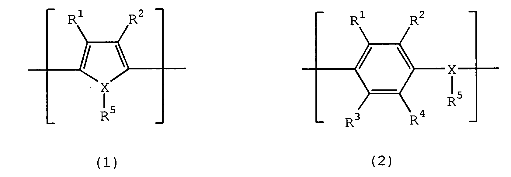
- organic semiconductor used as the cathode in the present invention include an organic semiconductor comprising benzopyrroline tetramer and chloranile, an organic semiconductor mainly comprising tetrathiotetracene, an organic semiconductor mainly comprising tetracyanoquinodimethane, and an organic semiconductor mainly comprising an electrically conducting polymer obtained by doping a dopant to a polymer containing a repeating unit represented by the following formula (1) or (2) : wherein R 1 to R 4 , which may be the same or different, each independently represents a hydrogen atom, an alkyl group having from 1 to 6 carbon atoms or an alkoxy group having from 1 to 6 carbon atoms, X represents an oxygen atom, a sulfur atom or a nitrogen atom, R 5 is present only when X is a nitrogen atom, and represents a hydrogen atom or an alkyl group having from 1 to 6 carbon atoms, and each of the pairs of R 1 and R 2 , and R 3 and R 4 may
- Preferred examples of the electrically conducting polymer containing a repeating unit represented by formula (1) for use in the present invention include an electrically conducting polymer containing a structure unit represented by the following formula (3) as a repeating unit: wherein R 6 and R 7 each independently represents a hydrogen atom, a linear or branched, saturated or unsaturated alkyl group having from 1 to 6 carbon atoms, or a substituent for forming at least one 5-, 6- or 7-membered saturated hydrocarbon ring structure containing two oxygen atoms when the alkyl groups are combined with each other at an arbitrary position, and the ring structure includes a structure having a vinylene bond which may be substituted, and a phenylene structure which may be substituted.
- the electrically conducting polymer containing such a chemical structure is being electrically charged and a dopant is doped therein.
- a dopant for the dopant, known dopants can be used without limitation.
- Examples of the polymer containing a repeating unit represented by formula (1), (2) or (3) include polyaniline, polyoxyphenylene, polyphenylene sulfide, polythiophene, polyfuran, polypyrrole, polymethylpyrrole, and substitution derivatives and copolymers thereof.
- preferred are polypyrrole, polythiophene and substitution derivatives thereof (e.g., poly(3,4-ethylenedioxythiophene)).
- the produced capacitor can have a small ESR value and this is preferred.
- an electrically conducting layer may be formed on the semiconductor layer formed by the above-described method, so that good electrical contact with the external drawing-out lead (for example, lead frame) can be obtained.
- the electrically conducting layer can be formed, for example, by the solidification of an electrically conducting paste, plating, metallization, or formation of a heat-resistant electrically conducting resin film.
- Preferred examples of the electrically conducting paste include silver paste, copper paste, aluminum paste, carbon paste and nickel paste, and these may be used individually or in combination of two or more thereof. In the case of using two or more pastes, the pastes may be mixed or may be superposed one on another as separate layers.
- the electrically conducting paste applied is then solidified by allowing it to stand in air or under heating.
- the plating include nickel plating, copper plating, silver plating and aluminum plating.
- the metal vapor-deposited include aluminum, nickel, copper and silver.
- carbon paste and silver paste are stacked in this order on the other electrode and then, the entirety is molded with a material such as epoxy resin, thereby fabricating a solid electrolytic capacitor.
- the capacitor having such a constitution of the present invention is jacketed, for example, by resin mold, resin case, metallic jacket case, resin dipping or laminate film and thereby, can be completed as a capacitor product for various uses.
- the capacitor produced in the present invention can be preferably used, for example, for circuits using a high-capacitance capacitor, such as an electric power circuit. These circuits can be used in various digital devices such as a personal computer, server, camera, game machine, DVD, AV equipment and cellular phone, and electrical devices such as various electric power sources.
- a high-capacitance capacitor such as an electric power circuit.
- These circuits can be used in various digital devices such as a personal computer, server, camera, game machine, DVD, AV equipment and cellular phone, and electrical devices such as various electric power sources.
- the leakage current hardly increases after mounting and therefore, by using this solid electrolytic capacitor, electronic circuits and electronic devices having less initial failure can be obtained.
- a niobium primary powder (average particle size: 0.8 ⁇ m) ground by utilizing the hydrogen embrittlement of a niobium ingot was granulated to obtain a niobium powder having an average particle size of 100 ⁇ m (this was a fine powder and therefore, naturally oxidized to contain 35,000 ppm of oxygen).
- the obtained niobium powder was left standing in a nitrogen atmosphere at 500°C and then in Ar at 700°C to provide a partially nitrided niobium powder (CV: 82,000/g) having a nitrided amount of 10,000 ppm.
- the resulting niobium powder was molded together with a 0.29mm ⁇ niobium wire and then sintered at 1,320°C.
- each sintered body was electrochemically formed in an aqueous 0.1% phosphoric acid solution for 7 hours under conditions of 80°C and 18 V to form a dielectric layer mainly comprising niobium oxide on the anode surface.
- the resulting anode having formed thereon a dielectric layer was heat-treated by leaving it in a furnace at a temperature shown in Table 1 under atmospheric pressure and thereafter, re-electrochemically formed in an aqueous 0.1% phosphoric acid solution under conditions of 80°C and 13 V.
- the re-electrochemical formation time, the number of operations of performing heat-treatment and re-electrochemical formation, and the LC value after final re-electrochemical formation are shown in Table 1.
- the anode was subjected to electrolytic polymerization in an aqueous solution having dissolved therein a pyrrole monomer and anthraquinonesulfonic acid to form a semiconductor (cathode) comprising polypyrrole.
- the stacked body was placed on a separately prepared lead frame working out to an external electrode such that the lead wire in the anode side and the silver paste part in the cathode side were lying on two protruded portions of the lead frame, respectively.
- the lead wire in the anode side and the silver paste part in the cathode side were then electrically/mechanically connected by spot-welding for the former and with silver paste for the latter.
- the entirety excluding a part of the lead frame was transfer-molded with epoxy resin and the lead frame outside the mold was cut and processed to produce a chip solid electrolytic capacitor having a size of 7.3 ⁇ 4.3 ⁇ 2.8 mm.
- Solid electrolytic capacitors were produced in the same manner as in Example 1 except that all heat-treatments were performed in water vapor.
- a petri dish having an inside diameter of 80mm ⁇ and containing water in it was left standing in a heat treatment furnace (internal diameter: 400 ⁇ 400 ⁇ 400 mm) to thereby obtain the water vapor. After the air in the furnace was sufficiently purged with water vapor, the heat treatment was performed.
- Solid electrolytic capacitors were produced in the same manner as in Example 1 except that all heat-treatments were performed in a furnace filled with a 15% oxygen gas diluted with argon gas.
- Solid electrolytic capacitors were produced in the same manner as in Example 1 except that a niobium powder having a CV value of 120,000/g was used, all heat-treatments were performed in a furnace filled with a 45% oxygen gas diluted with argon, and the electrolytic polymerization was performed by using an ethylenedioxythiophene monomer in place of the pyrrole monomer to change the semiconductor to polyethylenedioxythiophene.
- Solid electrolytic capacitors were produced in the same manner as in Example 1 except that neither heat-treatment nor re-electrochemical formation was performed (Comparative Example 1), re-electrochemical formation was performed once without performing heat-treatment (Comparative Example 2), heat-treatment was performed without performing re-electrochemical formation (Comparative Example 3), or heat-treatment and re-electrochemical formation each was performed once (Comparative Example 4).
- Solid electrolytic capacitors were produced in the same manner as in Example 1 except that the heat-treatment temperature was changed to 180°C.
- Solid electrolytic capacitors were produced in the same manner as in Example 1 except that the re-electrochemical formation time was shortened to give an LC value of 1.1 nA/CV after the final re-electrochemical formation.
- a niobium-tantalum primary powder having an average particle size of 0.6 ⁇ m which was obtained by grinding niobium-tantalum alloy in place of a niobium ingot in Example 1, was granulated to obtain a niobium-tantalum alloy powder having an average particle size of 120 ⁇ m (naturally oxidized to contain 30,000 ppm of oxygen).
- the obtained niobium-tantalum alloy powder was left standing in a nitrogen atmosphere to provide a partially nitrided niobium-tantalum alloy powder (CV: 79,000/g) having a nitrided amount of 8,500 ppm.
- the resulting niobium-tantalum alloy powder was molded together with a 0.40mm ⁇ niobium wire and then sintered at 1,360°C.
- plural sintered bodies were produced (the shape of the sintered body was the same as in Example 1 and the niobium wire was protruded by 3.2mm to the inside of the sintered body and by 10mm to the outside).
- each sintered body was electrochemically formed, heat-treated, electrochemically formed again, to form a semiconductor layer and to produce a capacitor under the same conditions in Example 1.
- a niobium-zirconium primary powder having an average particle size of 0.8 ⁇ m which was obtained by grinding niobium-zirconium alloy (98% by mass of niobium) in place of a niobium ingot in Example 1, was granulated to obtain a niobium-zirconium alloy powder having an average particle size of 160 ⁇ m (naturally oxidized to contain 45,000 ppm of oxygen).
- the obtained niobium-zirconium alloy powder was left standing in a nitrogen atmosphere at 600°C and then in Ar under the same conditions in Example 1 to provide a partially nitrided niobium-zirconium alloy powder (CV: 85,000/g) having a nitrided amount of 18,500 ppm.
- the resulting niobium-zirconium alloy powder was molded together with a 0.45mm ⁇ niobium wire and then sintered at 1,340°C. In this way, plural sintered bodies were produced (the shape of the sintered body was the same as in Example 1 and the niobium wire was protruded by 3.2mm to the inside of the sintered body and by 10mm to the outside).
- each sintered body was electrochemically formed, heat-treated, electrochemically formed again, to form a semiconductor layer and to produce a capacitor under the same conditions in Example 1 except that the heat-treatment was performed in the atmosphere containing oxygen gas in an amount of 30%.
- a niobium-silicon primary powder having an average particle size of 0.7 ⁇ m which was obtained by grinding niobium-silicon alloy (96% by mass of niobium) in place of a niobium ingot in Example 1, was granulated to obtain a niobium-silicon alloy powder having an average particle size of 90 ⁇ m (naturally oxidized to contain 40,000 ppm of oxygen).
- the obtained niobium-silicon alloy powder (CV: 130,000/g) was not left standing in a nitrogen atmosphere.
- the resulting niobium-silicon alloy powder was molded together with a 0.40mm ⁇ niobium wire and then sintered at 1,300°C.
- each sintered body was electrochemically formed, heat-treated, electrochemically formed again, to form a semiconductor layer and to produce a capacitor under the same conditions in Example 9.
- the initial performance and LC value (at 4 V) after mounting of each solid electrolytic capacitor produced in Examples 1 to 15 and Comparative Examples 1 to 5 are shown in Table 2.
- the mounting was performed by a method of attaching the solid electrolytic capacitor to a circuit board by cream soldering and passing the circuit board three times through a reflow furnace having a temperature pattern with a maximum temperature of 260°C (230°C, 30 seconds).
- the LC value after mounting was a value within 30 minutes after passing through the reflow furnace.
- a solid electrolytic capacitor improved in the leakage current (LC) value after mounting comprising repeating twice or more the steps of exposing the dielectric layer to a temperature of 200 to 1,000°C before the cathode comprising an organic semiconductor is formed and then re-electrochemically forming the dielectric layer.
Abstract
Description


| Heat Treatment | Re-Electrochemical Formation Time, min. | Total Number of Operations (times) | LC/CV after Final Re-Electrochemical Formation, nA/µFV | |||
| Temperature, °C | Time, min. | |||||
| Example | 1 | 250 | 10 | 10 | 40 | 0.13 |
| 2 | 250 | 100 | 10 | 40 | 0.18 | |
| 3 | 290 | 10 | 10 | 30 | 0.12 | |
| 4 | 290 | 100 | 10 | 30 | 0.17 | |
| 5 | 290 | 10 | 50 | 30 | 0.09 | |
| 6 | 380 | 10 | 10 | 15 | 0.20 | |
| 7 | 500 | 10 | 100 | 10 | 0.51 | |
| 8 | 210 | 10 | 10 | 55 | 0.23 | |
| 9 | 250 | 10 | 10 | 40 | 0.12 | |
| 10 | 250 | 10 | 10 | 40 | 0.10 | |
| 11 | 250 | 10 | 10 | 40 | 0.24 | |
| 12 | 250 | 10 | 10 | 40 | 1.10 | |
| 13 | 250 | 10 | 10 | 40 | 0.09 | |
| 14 | 250 | 10 | 10 | 40 | 0.12 | |
| 15 | 250 | 10 | 10 | 40 | 0.33 | |
| Comparative Example | 1 | - | - | - | 0 | 1.12 |
| 2 | - | - | 10 | 0 | 0.14 | |
| 3 | 250 | 10 | - | 0 | 1.61 | |
| 4 | 250 | 10 | 10 | 1 | 0.40 | |
| 5 | 180 | 10 | 10 | 40 | 0.16 |
| Initial Value of Product | LC after Mounting, µA | LC Rate of Change, LC after Mounting / Initial LC | |||
| capacitance, µF | LC, µA | ||||
| Example | 1 | 328 | 17 | 43 | 2.5 |
| 2 | 330 | 21 | 53 | 2.5 | |
| 3 | 325 | 15 | 41 | 2.7 | |
| 4 | 320 | 20 | 55 | 2.8 | |
| 5 | 326 | 13 | 40 | 3.1 | |
| 6 | 318 | 16 | 58 | 3.6 | |
| 7 | 307 | 15 | 71 | 4.7 | |
| 8 | 333 | 19 | 57 | 3.0 | |
| 9 | 320 | 17 | 34 | 2.0 | |
| 10 | 321 | 16 | 36 | 2.3 | |
| 11 | 466 | 26 | 66 | 2.5 | |
| 12 | 319 | 84 | 148 | 1.8 | |
| 13 | 320 | 8 | 13 | 1.6 | |
| 14 | 340 | 16 | 31 | 1.9 | |
| 15 | 550 | 27 | 68 | 2.5 | |
| Comparative Example | 1 | 323 | 128 | 1231 | 9.6 |
| 2 | 330 | 19 | 287 | 15.1 | |
| 3 | 322 | 215 | 1634 | 7.6 | |
| 4 | 334 | 15 | 186 | 12.4 | |
| 5 | 328 | 28 | 179 | 6.4 |
Claims (18)
- A method for producing a solid electrolytic capacitor comprising an anode, a dielectric layer and a cathode formed on the dielectric layer, the anode being at least one member selected from niobium monoxide, niobium and an alloy mainly comprising niobium, or a mixture of niobium monoxide with niobium or an alloy mainly comprising niobium, the dielectric layer being a layer formed by the electrolytic oxidation (electrochemical formation) of the anode, and the cathode being an organic semiconductor, the method comprising sequentially repeating twice or more a step of exposing the dielectric layer to a temperature of 200 to 1,000°C before formation of the cathode and a step of re-electrochemically forming the dielectric layer.
- The method for producing a solid electrolytic capacitor as claimed in claim 1, wherein the step of exposing the dielectric layer to a temperature of 200 to 1,000°C is performed in the atmosphere containing water vapor.
- The method for producing a solid electrolytic capacitor as claimed in claim 1 or 2, wherein the step of exposing the dielectric layer to a temperature of 200 to 1,000°C is performed in the atmosphere containing oxygen gas of 5% by volume or more.
- The method for producing a solid electrolytic capacitor as claimed in any one of claims 1 to 3, wherein the leakage current value of the dielectric layer after re-electrochemical formation is 1 nA/CV or less.
- The method for producing a solid electrolytic capacitor as claimed in claims 1, wherein the organic semiconductor is at least one selected from an organic semiconductor comprising benzopyrroline tetramer and chloranile, an organic semiconductor mainly comprising tetrathiotetracene, an organic semiconductor mainly comprising tetracyanoquinodimethane, and an organic semiconductor mainly comprising an electrically conducting polymer obtained by doping a dopant to a polymer containing a repeating unit represented by the following formula (1) or (2) :wherein R1 to R4, which may be the same or different, each independently represents a hydrogen atom, an alkyl group having from 1 to 6 carbon atoms or an alkoxy group having from 1 to 6 carbon atoms, X represents an oxygen atom, a sulfur atom or a nitrogen atom, R5 is present only when X is a nitrogen atom, and represents a hydrogen atom or an alkyl group having from 1 to 6 carbon atoms, and each of the pairs of R1 and R2, and R3 and R4 may combine with each other to form a ring structure.
- The method for producing a solid electrolytic capacitor as claimed in claim 5, wherein the polymer containing a repeating unit represented by formula (1) is polymer containing a structure unit represented by the following formula (3) as a repeating unit:wherein R6 and R7 each independently represents a hydrogen atom, a linear or branched, saturated or unsaturated alkyl group having from 1 to 6 carbon atoms, or a substituent for forming at least one 5-, 6- or 7-membered saturated hydrocarbon ring structure containing two oxygen atoms when the alkyl groups are combined with each other at an arbitrary position, and the ring structure includes a structure having a vinylene bond which may be substituted, and a phenylene structure which may be substituted.

- The method for producing a solid electrolytic capacitor as claimed in claim 5, wherein the polymer is selected from polyaniline, polyoxyphenylene, polyphenylene sulfide, polythiophene, polyfuran, polypyrrole, polymethylpyrrole, and substitution derivatives and copolymers thereof.
- The method for producing a solid electrolytic capacitor as claimed in claim 7, wherein the polymer is poly(3,4-ethylenedioxythiophene).
- The method for producing a solid electrolytic capacitor as claimed in claim 1, wherein the organic semiconductor has an electrical conductivity of 10-1 to 103 S/cm.
- The method for producing a solid electrolytic capacitor as claimed in claim 1, wherein the anode is a sintered body or a foil.
- The method for producing a solid electrolytic capacitor as claimed in claim 1, wherein the alloy mainly comprising niobium is selected from niobium-tantalum alloy, niobium-zirconium alloy or niobium-silicon alloy.
- The method for producing a solid electrolytic capacitor as claimed in claim 10, wherein the specific surface area of the sintered body is from 0.2 to 7 m2/g.
- The method for producing a solid electrolytic capacitor as claimed in claim 1, wherein a lead wire formed of a material selected from niobium, partially nitrided niobium, partially oxidized niobium and tantalum is electrically or mechanically connected to the anode.
- The method for producing a solid electrolytic capacitor as claimed in claim 1, wherein the exposure of the dielectric layer to a temperature of 200 to 1,000°C is performed for 10 seconds to 100 hours.
- The method for producing a solid electrolytic capacitor as claimed in claim 1, wherein an electrically conducting layer is formed on an organic semiconductor layer.
- A solid electrolytic capacitor produced by the production method claimed in any one of claims 1 to 15.
- An electronic circuit using the solid electrolytic capacitor claimed in claim 16.
- An electronic device using the solid electrolytic capacitor claimed in claim 16.
Applications Claiming Priority (3)
| Application Number | Priority Date | Filing Date | Title |
|---|---|---|---|
| JP2003023072 | 2003-01-31 | ||
| JP2003023072 | 2003-01-31 | ||
| PCT/JP2004/000925 WO2004068517A1 (en) | 2003-01-31 | 2004-01-30 | Method for manufacturing solid electrolytic capacitor |
Publications (3)
| Publication Number | Publication Date |
|---|---|
| EP1592030A1 true EP1592030A1 (en) | 2005-11-02 |
| EP1592030A4 EP1592030A4 (en) | 2009-04-29 |
| EP1592030B1 EP1592030B1 (en) | 2012-01-11 |
Family
ID=32820709
Family Applications (1)
| Application Number | Title | Priority Date | Filing Date |
|---|---|---|---|
| EP04706862A Expired - Lifetime EP1592030B1 (en) | 2003-01-31 | 2004-01-30 | Method for manufacturing solid electrolytic capacitor |
Country Status (6)
| Country | Link |
|---|---|
| US (1) | US6882522B2 (en) |
| EP (1) | EP1592030B1 (en) |
| JP (1) | JP4596543B2 (en) |
| AT (1) | ATE541300T1 (en) |
| TW (1) | TW200503023A (en) |
| WO (1) | WO2004068517A1 (en) |
Cited By (1)
| Publication number | Priority date | Publication date | Assignee | Title |
|---|---|---|---|---|
| WO2009042394A1 (en) * | 2007-09-24 | 2009-04-02 | Medtronic, Inc. | Tantalum anodes for high voltage capacitors employed by implantable medical devices and fabrication thereof |
Families Citing this family (20)
| Publication number | Priority date | Publication date | Assignee | Title |
|---|---|---|---|---|
| JP2004143477A (en) * | 2002-10-22 | 2004-05-20 | Cabot Supermetal Kk | Niobium powder and production method therefor, and solid electrolytic capacitor obtained by using the same |
| KR20060039924A (en) * | 2003-07-31 | 2006-05-09 | 가부시키가이샤 가네카 | Method for forming oxide film on metal surface using ionic liquid, elelctrolytic capacitor and electrolyte thereof |
| US7169284B1 (en) * | 2003-09-22 | 2007-01-30 | Pacesetter, Inc. | High surface area cathode for electrolytic capacitors using conductive polymer |
| PT1524678E (en) * | 2003-10-17 | 2009-10-19 | Starck H C Gmbh | Electrolytic capacitors with polymeric outer layer |
| US7715174B1 (en) * | 2004-05-17 | 2010-05-11 | Pacesetter, Inc. | Electrolytic capacitors with alternate cathode materials for use in pulse discharge applications |
| JP4689222B2 (en) * | 2004-09-22 | 2011-05-25 | 信越ポリマー株式会社 | Conductive coating film and method for producing the same |
| JP4519679B2 (en) * | 2005-02-21 | 2010-08-04 | Necトーキン株式会社 | Conductive polymer composition and solid electrolytic capacitor using the same |
| JP4508913B2 (en) * | 2005-03-23 | 2010-07-21 | 三洋電機株式会社 | Solid electrolytic capacitor and method for producing anode material for solid electrolytic capacitor |
| DE102005033839A1 (en) * | 2005-07-20 | 2007-01-25 | H.C. Starck Gmbh | Electrolytic capacitors with a polymeric outer layer and process for their preparation |
| WO2007020464A1 (en) * | 2005-08-19 | 2007-02-22 | Avx Limited | Solid state capacitors and method of manufacturing them |
| DE102005043828A1 (en) * | 2005-09-13 | 2007-03-22 | H.C. Starck Gmbh | Process for the preparation of electrolytic capacitors |
| DE102005043829A1 (en) * | 2005-09-13 | 2007-04-05 | H.C. Starck Gmbh | Process for the production of electrolytic capacitors with high nominal voltage |
| JP4671350B2 (en) * | 2005-10-28 | 2011-04-13 | ニチコン株式会社 | Solid electrolytic capacitor and manufacturing method thereof |
| JP4811014B2 (en) * | 2005-12-16 | 2011-11-09 | 株式会社村田製作所 | Drying equipment for manufacturing solid electrolytic capacitor elements |
| US8027150B2 (en) * | 2007-02-09 | 2011-09-27 | Kaneka Corporation | Conductive polymer solid electrolytic capacitor |
| US7876548B2 (en) | 2007-04-20 | 2011-01-25 | Sanyo Electric Co., Ltd. | Niobium solid electrolytic capacitor and its production method |
| DE102007048212A1 (en) * | 2007-10-08 | 2009-04-09 | H.C. Starck Gmbh | Process for the preparation of electrolytic capacitors with polymeric interlayer |
| DE102008063853B4 (en) | 2008-12-19 | 2012-08-30 | H.C. Starck Gmbh | capacitor anode |
| JPWO2011013375A1 (en) * | 2009-07-29 | 2013-01-07 | 昭和電工株式会社 | Manufacturing method of solid electrolytic capacitor |
| JP2017212281A (en) * | 2016-05-24 | 2017-11-30 | 国立大学法人北海道大学 | Capacitor and manufacturing method thereof |
Citations (5)
| Publication number | Priority date | Publication date | Assignee | Title |
|---|---|---|---|---|
| JPH02267915A (en) * | 1989-04-07 | 1990-11-01 | Hitachi Aic Inc | Manufacture of solid-state electrolytic capacitor |
| JPH0684709A (en) * | 1992-09-03 | 1994-03-25 | Rohm Co Ltd | Manufacture of solid electrolytic capacitor |
| US20010036056A1 (en) * | 1998-09-16 | 2001-11-01 | Kimmel Jonathon L. | Methods to partially reduce a niobium metal oxide and oxygen reduced niobium oxides |
| JP2002246273A (en) * | 2001-02-14 | 2002-08-30 | Matsushita Electric Ind Co Ltd | Method for producing solid electrolytic capacitor |
| EP1340235B1 (en) * | 2000-11-30 | 2006-08-09 | Showa Denko K.K. | Powder for capacitor, sintered body thereof and capacitor using the sintered body |
Family Cites Families (14)
| Publication number | Priority date | Publication date | Assignee | Title |
|---|---|---|---|---|
| JPS59115517A (en) * | 1982-12-22 | 1984-07-04 | 日本電気株式会社 | Method of producing electrolytic condenser |
| JPS60147110A (en) * | 1984-01-11 | 1985-08-03 | 日本電気株式会社 | Method of producing electrolytic condenser |
| US4805074A (en) * | 1987-03-20 | 1989-02-14 | Nitsuko Corporation | Solid electrolytic capacitor, and method of manufacturing same |
| JPH0638385B2 (en) * | 1989-06-23 | 1994-05-18 | エルナー株式会社 | Method for manufacturing electrode foil for aluminum electrolytic capacitor |
| JP3250310B2 (en) | 1993-03-26 | 2002-01-28 | 松下電器産業株式会社 | Method of forming anode foil for aluminum electrolytic capacitor |
| JP3216477B2 (en) | 1995-04-24 | 2001-10-09 | 松下電器産業株式会社 | Method for producing electrode foil for aluminum electrolytic capacitor |
| US5812367A (en) * | 1996-04-04 | 1998-09-22 | Matsushita Electric Industrial Co., Ltd. | Solid electrolytic capacitors comprising a conductive layer made of a polymer of pyrrole or its derivative |
| JP3255091B2 (en) * | 1997-08-28 | 2002-02-12 | 松下電器産業株式会社 | Method for manufacturing solid electrolytic capacitor |
| JP3974706B2 (en) * | 1998-03-24 | 2007-09-12 | 富士通メディアデバイス株式会社 | Manufacturing method of solid electrolytic capacitor |
| JP2001110681A (en) * | 1999-10-12 | 2001-04-20 | Fujitsu Media Device Kk | Solid electrolytic capacitor and method for manufacturing the same |
| US6552896B1 (en) * | 1999-10-28 | 2003-04-22 | Matsushita Electric Industrial Co., Ltd. | Solid electrolytic capacitor and method for manufacturing the same |
| JP2002093666A (en) * | 2000-09-20 | 2002-03-29 | Showa Denko Kk | Niobium powder, sintered compact using the same and capacitor using the compact |
| JP4453890B2 (en) * | 2001-04-12 | 2010-04-21 | 昭和電工株式会社 | Niobium capacitor manufacturing method. |
| JP2002367867A (en) * | 2001-06-06 | 2002-12-20 | Matsushita Electric Ind Co Ltd | Electrode member for solid electrolytic capacitor, method of manufacturing it and solid electrolytic capacitor using this |
-
2004
- 2004-01-30 JP JP2005504772A patent/JP4596543B2/en not_active Expired - Fee Related
- 2004-01-30 EP EP04706862A patent/EP1592030B1/en not_active Expired - Lifetime
- 2004-01-30 AT AT04706862T patent/ATE541300T1/en active
- 2004-01-30 WO PCT/JP2004/000925 patent/WO2004068517A1/en active Application Filing
- 2004-01-30 TW TW093102226A patent/TW200503023A/en not_active IP Right Cessation
- 2004-01-30 US US10/767,382 patent/US6882522B2/en not_active Expired - Lifetime
Patent Citations (5)
| Publication number | Priority date | Publication date | Assignee | Title |
|---|---|---|---|---|
| JPH02267915A (en) * | 1989-04-07 | 1990-11-01 | Hitachi Aic Inc | Manufacture of solid-state electrolytic capacitor |
| JPH0684709A (en) * | 1992-09-03 | 1994-03-25 | Rohm Co Ltd | Manufacture of solid electrolytic capacitor |
| US20010036056A1 (en) * | 1998-09-16 | 2001-11-01 | Kimmel Jonathon L. | Methods to partially reduce a niobium metal oxide and oxygen reduced niobium oxides |
| EP1340235B1 (en) * | 2000-11-30 | 2006-08-09 | Showa Denko K.K. | Powder for capacitor, sintered body thereof and capacitor using the sintered body |
| JP2002246273A (en) * | 2001-02-14 | 2002-08-30 | Matsushita Electric Ind Co Ltd | Method for producing solid electrolytic capacitor |
Non-Patent Citations (1)
| Title |
|---|
| See also references of WO2004068517A1 * |
Cited By (2)
| Publication number | Priority date | Publication date | Assignee | Title |
|---|---|---|---|---|
| WO2009042394A1 (en) * | 2007-09-24 | 2009-04-02 | Medtronic, Inc. | Tantalum anodes for high voltage capacitors employed by implantable medical devices and fabrication thereof |
| US7837743B2 (en) | 2007-09-24 | 2010-11-23 | Medtronic, Inc. | Tantalum anodes for high voltage capacitors employed by implantable medical devices and fabrication thereof |
Also Published As
| Publication number | Publication date |
|---|---|
| ATE541300T1 (en) | 2012-01-15 |
| WO2004068517A1 (en) | 2004-08-12 |
| US6882522B2 (en) | 2005-04-19 |
| TW200503023A (en) | 2005-01-16 |
| JP4596543B2 (en) | 2010-12-08 |
| EP1592030B1 (en) | 2012-01-11 |
| TWI327326B (en) | 2010-07-11 |
| EP1592030A4 (en) | 2009-04-29 |
| JPWO2004068517A1 (en) | 2006-05-25 |
| US20040233614A1 (en) | 2004-11-25 |
Similar Documents
| Publication | Publication Date | Title |
|---|---|---|
| US6882522B2 (en) | Production method of solid electrolytic capacitor | |
| US7122063B2 (en) | Capacitor and production method of the capacitor | |
| US20090027834A1 (en) | Solid electrolyte capacitor | |
| EP1876612B1 (en) | Solid electrolytic capacitor element, method for manufacturing same, and solid electrolytic capacitor | |
| EP1898433B1 (en) | Solid electrolytic capacitor and production method thereof | |
| US7522404B2 (en) | Solid electrolytic capacitor and the use thereof | |
| US7218505B2 (en) | Chip solid electrolyte capacitor | |
| EP1654745B1 (en) | Chip solid electrolyte capcitor and production method of the same | |
| US7361202B2 (en) | Tantalum sintered body and capacitor using the sintered body | |
| US7355842B2 (en) | Chip solid electrolyte capacitor and production method of the same | |
| US20090090997A1 (en) | Solid electrolytic capacitor element and production method thereof | |
| JP4451235B2 (en) | Manufacturing method of solid electrolytic capacitor | |
| US7291537B2 (en) | Method for producing solid electrolytic capacitor | |
| JP4367752B2 (en) | Method for manufacturing solid electrolytic capacitor element | |
| WO2005008701A1 (en) | Method for producing solid electrolytic capacitor | |
| KR20060058719A (en) | Chip solid electrolyte capacitor and production method of the same |
Legal Events
| Date | Code | Title | Description |
|---|---|---|---|
| PUAI | Public reference made under article 153(3) epc to a published international application that has entered the european phase |
Free format text: ORIGINAL CODE: 0009012 |
|
| 17P | Request for examination filed |
Effective date: 20050819 |
|
| AK | Designated contracting states |
Kind code of ref document: A1 Designated state(s): AT BE BG CH CY CZ DE DK EE ES FI FR GB GR HU IE IT LI LU MC NL PT RO SE SI SK TR |
|
| AX | Request for extension of the european patent |
Extension state: AL LT LV MK |
|
| DAX | Request for extension of the european patent (deleted) | ||
| A4 | Supplementary search report drawn up and despatched |
Effective date: 20090326 |
|
| 17Q | First examination report despatched |
Effective date: 20100630 |
|
| GRAP | Despatch of communication of intention to grant a patent |
Free format text: ORIGINAL CODE: EPIDOSNIGR1 |
|
| RIN1 | Information on inventor provided before grant (corrected) |
Inventor name: KABE, ISAO Inventor name: NAITO, KAZUMI |
|
| GRAS | Grant fee paid |
Free format text: ORIGINAL CODE: EPIDOSNIGR3 |
|
| GRAA | (expected) grant |
Free format text: ORIGINAL CODE: 0009210 |
|
| AK | Designated contracting states |
Kind code of ref document: B1 Designated state(s): AT BE BG CH CY CZ DE DK EE ES FI FR GB GR HU IE IT LI LU MC NL PT RO SE SI SK TR |
|
| REG | Reference to a national code |
Ref country code: GB Ref legal event code: FG4D |
|
| REG | Reference to a national code |
Ref country code: CH Ref legal event code: EP |
|
| REG | Reference to a national code |
Ref country code: AT Ref legal event code: REF Ref document number: 541300 Country of ref document: AT Kind code of ref document: T Effective date: 20120115 |
|
| REG | Reference to a national code |
Ref country code: IE Ref legal event code: FG4D |
|
| REG | Reference to a national code |
Ref country code: DE Ref legal event code: R096 Ref document number: 602004036079 Country of ref document: DE Effective date: 20120315 |
|
| REG | Reference to a national code |
Ref country code: NL Ref legal event code: VDEP Effective date: 20120111 |
|
| PG25 | Lapsed in a contracting state [announced via postgrant information from national office to epo] |
Ref country code: SI Free format text: LAPSE BECAUSE OF FAILURE TO SUBMIT A TRANSLATION OF THE DESCRIPTION OR TO PAY THE FEE WITHIN THE PRESCRIBED TIME-LIMIT Effective date: 20120111 |
|
| PG25 | Lapsed in a contracting state [announced via postgrant information from national office to epo] |
Ref country code: BG Free format text: LAPSE BECAUSE OF FAILURE TO SUBMIT A TRANSLATION OF THE DESCRIPTION OR TO PAY THE FEE WITHIN THE PRESCRIBED TIME-LIMIT Effective date: 20120411 Ref country code: BE Free format text: LAPSE BECAUSE OF FAILURE TO SUBMIT A TRANSLATION OF THE DESCRIPTION OR TO PAY THE FEE WITHIN THE PRESCRIBED TIME-LIMIT Effective date: 20120111 Ref country code: NL Free format text: LAPSE BECAUSE OF FAILURE TO SUBMIT A TRANSLATION OF THE DESCRIPTION OR TO PAY THE FEE WITHIN THE PRESCRIBED TIME-LIMIT Effective date: 20120111 |
|
| PG25 | Lapsed in a contracting state [announced via postgrant information from national office to epo] |
Ref country code: GR Free format text: LAPSE BECAUSE OF FAILURE TO SUBMIT A TRANSLATION OF THE DESCRIPTION OR TO PAY THE FEE WITHIN THE PRESCRIBED TIME-LIMIT Effective date: 20120412 Ref country code: MC Free format text: LAPSE BECAUSE OF NON-PAYMENT OF DUE FEES Effective date: 20120131 Ref country code: FI Free format text: LAPSE BECAUSE OF FAILURE TO SUBMIT A TRANSLATION OF THE DESCRIPTION OR TO PAY THE FEE WITHIN THE PRESCRIBED TIME-LIMIT Effective date: 20120111 Ref country code: PT Free format text: LAPSE BECAUSE OF FAILURE TO SUBMIT A TRANSLATION OF THE DESCRIPTION OR TO PAY THE FEE WITHIN THE PRESCRIBED TIME-LIMIT Effective date: 20120511 |
|
| REG | Reference to a national code |
Ref country code: CH Ref legal event code: PL |
|
| REG | Reference to a national code |
Ref country code: AT Ref legal event code: MK05 Ref document number: 541300 Country of ref document: AT Kind code of ref document: T Effective date: 20120111 |
|
| PG25 | Lapsed in a contracting state [announced via postgrant information from national office to epo] |
Ref country code: CY Free format text: LAPSE BECAUSE OF FAILURE TO SUBMIT A TRANSLATION OF THE DESCRIPTION OR TO PAY THE FEE WITHIN THE PRESCRIBED TIME-LIMIT Effective date: 20120111 |
|
| REG | Reference to a national code |
Ref country code: IE Ref legal event code: MM4A |
|
| PG25 | Lapsed in a contracting state [announced via postgrant information from national office to epo] |
Ref country code: RO Free format text: LAPSE BECAUSE OF FAILURE TO SUBMIT A TRANSLATION OF THE DESCRIPTION OR TO PAY THE FEE WITHIN THE PRESCRIBED TIME-LIMIT Effective date: 20120111 Ref country code: CZ Free format text: LAPSE BECAUSE OF FAILURE TO SUBMIT A TRANSLATION OF THE DESCRIPTION OR TO PAY THE FEE WITHIN THE PRESCRIBED TIME-LIMIT Effective date: 20120111 Ref country code: SE Free format text: LAPSE BECAUSE OF FAILURE TO SUBMIT A TRANSLATION OF THE DESCRIPTION OR TO PAY THE FEE WITHIN THE PRESCRIBED TIME-LIMIT Effective date: 20120111 Ref country code: DK Free format text: LAPSE BECAUSE OF FAILURE TO SUBMIT A TRANSLATION OF THE DESCRIPTION OR TO PAY THE FEE WITHIN THE PRESCRIBED TIME-LIMIT Effective date: 20120111 Ref country code: CH Free format text: LAPSE BECAUSE OF NON-PAYMENT OF DUE FEES Effective date: 20120131 Ref country code: LI Free format text: LAPSE BECAUSE OF NON-PAYMENT OF DUE FEES Effective date: 20120131 Ref country code: EE Free format text: LAPSE BECAUSE OF FAILURE TO SUBMIT A TRANSLATION OF THE DESCRIPTION OR TO PAY THE FEE WITHIN THE PRESCRIBED TIME-LIMIT Effective date: 20120111 |
|
| PLBE | No opposition filed within time limit |
Free format text: ORIGINAL CODE: 0009261 |
|
| STAA | Information on the status of an ep patent application or granted ep patent |
Free format text: STATUS: NO OPPOSITION FILED WITHIN TIME LIMIT |
|
| PG25 | Lapsed in a contracting state [announced via postgrant information from national office to epo] |
Ref country code: IT Free format text: LAPSE BECAUSE OF FAILURE TO SUBMIT A TRANSLATION OF THE DESCRIPTION OR TO PAY THE FEE WITHIN THE PRESCRIBED TIME-LIMIT Effective date: 20120111 Ref country code: SK Free format text: LAPSE BECAUSE OF FAILURE TO SUBMIT A TRANSLATION OF THE DESCRIPTION OR TO PAY THE FEE WITHIN THE PRESCRIBED TIME-LIMIT Effective date: 20120111 |
|
| 26N | No opposition filed |
Effective date: 20121012 |
|
| PG25 | Lapsed in a contracting state [announced via postgrant information from national office to epo] |
Ref country code: IE Free format text: LAPSE BECAUSE OF NON-PAYMENT OF DUE FEES Effective date: 20120130 Ref country code: AT Free format text: LAPSE BECAUSE OF FAILURE TO SUBMIT A TRANSLATION OF THE DESCRIPTION OR TO PAY THE FEE WITHIN THE PRESCRIBED TIME-LIMIT Effective date: 20120111 |
|
| REG | Reference to a national code |
Ref country code: DE Ref legal event code: R097 Ref document number: 602004036079 Country of ref document: DE Effective date: 20121012 |
|
| PG25 | Lapsed in a contracting state [announced via postgrant information from national office to epo] |
Ref country code: ES Free format text: LAPSE BECAUSE OF FAILURE TO SUBMIT A TRANSLATION OF THE DESCRIPTION OR TO PAY THE FEE WITHIN THE PRESCRIBED TIME-LIMIT Effective date: 20120422 |
|
| PGFP | Annual fee paid to national office [announced via postgrant information from national office to epo] |
Ref country code: FR Payment date: 20130204 Year of fee payment: 10 Ref country code: GB Payment date: 20130130 Year of fee payment: 10 |
|
| PG25 | Lapsed in a contracting state [announced via postgrant information from national office to epo] |
Ref country code: TR Free format text: LAPSE BECAUSE OF FAILURE TO SUBMIT A TRANSLATION OF THE DESCRIPTION OR TO PAY THE FEE WITHIN THE PRESCRIBED TIME-LIMIT Effective date: 20120111 |
|
| PG25 | Lapsed in a contracting state [announced via postgrant information from national office to epo] |
Ref country code: LU Free format text: LAPSE BECAUSE OF NON-PAYMENT OF DUE FEES Effective date: 20120130 |
|
| PG25 | Lapsed in a contracting state [announced via postgrant information from national office to epo] |
Ref country code: HU Free format text: LAPSE BECAUSE OF FAILURE TO SUBMIT A TRANSLATION OF THE DESCRIPTION OR TO PAY THE FEE WITHIN THE PRESCRIBED TIME-LIMIT Effective date: 20040130 |
|
| GBPC | Gb: european patent ceased through non-payment of renewal fee |
Effective date: 20140130 |
|
| REG | Reference to a national code |
Ref country code: FR Ref legal event code: ST Effective date: 20140930 |
|
| PG25 | Lapsed in a contracting state [announced via postgrant information from national office to epo] |
Ref country code: FR Free format text: LAPSE BECAUSE OF NON-PAYMENT OF DUE FEES Effective date: 20140131 Ref country code: GB Free format text: LAPSE BECAUSE OF NON-PAYMENT OF DUE FEES Effective date: 20140130 |
|
| PGFP | Annual fee paid to national office [announced via postgrant information from national office to epo] |
Ref country code: DE Payment date: 20180117 Year of fee payment: 15 |
|
| REG | Reference to a national code |
Ref country code: DE Ref legal event code: R119 Ref document number: 602004036079 Country of ref document: DE |
|
| PG25 | Lapsed in a contracting state [announced via postgrant information from national office to epo] |
Ref country code: DE Free format text: LAPSE BECAUSE OF NON-PAYMENT OF DUE FEES Effective date: 20190801 |