EP1592023A1 - Elément de mémoire vive magnétique - Google Patents
Elément de mémoire vive magnétique Download PDFInfo
- Publication number
- EP1592023A1 EP1592023A1 EP05103286A EP05103286A EP1592023A1 EP 1592023 A1 EP1592023 A1 EP 1592023A1 EP 05103286 A EP05103286 A EP 05103286A EP 05103286 A EP05103286 A EP 05103286A EP 1592023 A1 EP1592023 A1 EP 1592023A1
- Authority
- EP
- European Patent Office
- Prior art keywords
- magnetic
- layer
- ferromagnetic layers
- ferromagnetic
- memory element
- Prior art date
- Legal status (The legal status is an assumption and is not a legal conclusion. Google has not performed a legal analysis and makes no representation as to the accuracy of the status listed.)
- Withdrawn
Links
- 230000005291 magnetic effect Effects 0.000 title claims abstract description 349
- 230000015654 memory Effects 0.000 title claims abstract description 144
- 230000005294 ferromagnetic effect Effects 0.000 claims abstract description 118
- 239000013598 vector Substances 0.000 claims abstract description 84
- 238000000034 method Methods 0.000 claims abstract description 52
- 230000004888 barrier function Effects 0.000 claims abstract description 14
- 230000008569 process Effects 0.000 description 17
- 230000000694 effects Effects 0.000 description 14
- 230000003993 interaction Effects 0.000 description 14
- 230000005290 antiferromagnetic effect Effects 0.000 description 13
- 238000000926 separation method Methods 0.000 description 13
- 230000005415 magnetization Effects 0.000 description 12
- 230000008878 coupling Effects 0.000 description 10
- 238000010168 coupling process Methods 0.000 description 10
- 238000005859 coupling reaction Methods 0.000 description 10
- 230000003247 decreasing effect Effects 0.000 description 9
- 230000000875 corresponding effect Effects 0.000 description 7
- 239000003302 ferromagnetic material Substances 0.000 description 7
- 230000006399 behavior Effects 0.000 description 5
- 230000007423 decrease Effects 0.000 description 5
- 230000002349 favourable effect Effects 0.000 description 5
- XEEYBQQBJWHFJM-UHFFFAOYSA-N Iron Chemical compound [Fe] XEEYBQQBJWHFJM-UHFFFAOYSA-N 0.000 description 4
- 230000009471 action Effects 0.000 description 4
- 230000008901 benefit Effects 0.000 description 4
- 238000004364 calculation method Methods 0.000 description 4
- 238000004088 simulation Methods 0.000 description 4
- 230000008859 change Effects 0.000 description 3
- 230000004069 differentiation Effects 0.000 description 3
- 239000000463 material Substances 0.000 description 3
- 229910000640 Fe alloy Inorganic materials 0.000 description 2
- 230000015556 catabolic process Effects 0.000 description 2
- 239000004020 conductor Substances 0.000 description 2
- 238000006731 degradation reaction Methods 0.000 description 2
- 238000000151 deposition Methods 0.000 description 2
- 238000010586 diagram Methods 0.000 description 2
- 230000014509 gene expression Effects 0.000 description 2
- 230000000670 limiting effect Effects 0.000 description 2
- 230000014759 maintenance of location Effects 0.000 description 2
- 238000004519 manufacturing process Methods 0.000 description 2
- 229910052751 metal Inorganic materials 0.000 description 2
- 239000002184 metal Substances 0.000 description 2
- 230000004048 modification Effects 0.000 description 2
- 238000012986 modification Methods 0.000 description 2
- 238000005457 optimization Methods 0.000 description 2
- 230000010355 oscillation Effects 0.000 description 2
- 229910000531 Co alloy Inorganic materials 0.000 description 1
- 229910000990 Ni alloy Inorganic materials 0.000 description 1
- KJTLSVCANCCWHF-UHFFFAOYSA-N Ruthenium Chemical compound [Ru] KJTLSVCANCCWHF-UHFFFAOYSA-N 0.000 description 1
- 238000000137 annealing Methods 0.000 description 1
- 230000005316 antiferromagnetic exchange Effects 0.000 description 1
- 238000006243 chemical reaction Methods 0.000 description 1
- 230000008094 contradictory effect Effects 0.000 description 1
- 238000007796 conventional method Methods 0.000 description 1
- 230000002596 correlated effect Effects 0.000 description 1
- 230000008021 deposition Effects 0.000 description 1
- 238000013461 design Methods 0.000 description 1
- 238000002474 experimental method Methods 0.000 description 1
- 238000002513 implantation Methods 0.000 description 1
- 238000011423 initialization method Methods 0.000 description 1
- 230000010354 integration Effects 0.000 description 1
- 238000005468 ion implantation Methods 0.000 description 1
- 150000002500 ions Chemical class 0.000 description 1
- 230000002427 irreversible effect Effects 0.000 description 1
- 230000005389 magnetism Effects 0.000 description 1
- 239000011159 matrix material Substances 0.000 description 1
- 229940050561 matrix product Drugs 0.000 description 1
- 239000000203 mixture Substances 0.000 description 1
- 230000000737 periodic effect Effects 0.000 description 1
- 230000035699 permeability Effects 0.000 description 1
- 238000004321 preservation Methods 0.000 description 1
- 230000002829 reductive effect Effects 0.000 description 1
- 230000002441 reversible effect Effects 0.000 description 1
- 229910052707 ruthenium Inorganic materials 0.000 description 1
- 239000003381 stabilizer Substances 0.000 description 1
- 230000000087 stabilizing effect Effects 0.000 description 1
- 230000003068 static effect Effects 0.000 description 1
- 238000003860 storage Methods 0.000 description 1
- 230000009897 systematic effect Effects 0.000 description 1
- 238000012360 testing method Methods 0.000 description 1
- 238000012546 transfer Methods 0.000 description 1
- 238000011282 treatment Methods 0.000 description 1
Images

Classifications
-
- G—PHYSICS
- G11—INFORMATION STORAGE
- G11C—STATIC STORES
- G11C11/00—Digital stores characterised by the use of particular electric or magnetic storage elements; Storage elements therefor
- G11C11/02—Digital stores characterised by the use of particular electric or magnetic storage elements; Storage elements therefor using magnetic elements
- G11C11/16—Digital stores characterised by the use of particular electric or magnetic storage elements; Storage elements therefor using magnetic elements using elements in which the storage effect is based on magnetic spin effect
Definitions
- the present invention relates to a memory element magnetic live and in particular a memory element intended to be used in a magnetic RAM (MRAM of English Magnetic Random Access Memory) including a matrix of elements memory.
- MRAM Magnetic Random Access Memory
- An element of magnetic random access memory is characterized generally by a magnetic moment vector whose orientation can be modified by applying an original action outside, including a magnetic field.
- An information specific is stored in the memory element by orienting the vector magnetic moment according to a direction and / or a direction privileged.
- the memory element can retain information for a significant period of time without the need for refreshing the memory element or supplying it with energy, this which is an important advantage of this type of memory.
- to store a binary information it can be provided a memory element having an axis of easy magnetization. The magnetic moment vector is then oriented along the axis of easy magnetization in a first sense to store a first state of information and in the opposite direction to store a second state of the information.
- a conventional method of reading information stored in a magnetic random access memory element consists of detect the resistance differences of the memory element according to the orientation of the magnetic moment vector.
- a method The classical way of writing a memory element involves magnetic fields of writing produced by passing currents through metal tracks external to the element memory. Unconventionally, it has also been proposed to use the effects produced by a current sent through the memory element itself. Such effects include: magnetic field created by the current, an induced thermal effect by Joule effect, or a kinetic momentum transfer effect of spin electrons conduction towards magnetization.
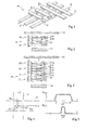
- Figure 1 represents the schematic diagram of a classic magnetic memory.
- the MRAM 10 is constituted first tracks of a conductive material forming lines of word 12 arranged perpendicularly to second tracks of a conductive material forming bit lines 14.
- the period p of the word line network 12 and the period p 'of the network of bit lines 14 are usually in the order of a few times the width w of a metal track and can to be different.
- a memory element 16 is arranged to the intersection of each word line 12 and each line of bit 14. The writing process then involves fields magnetic products by passing currents through the word lines 12 and the bit lines 14.
- a realistic diagram of a magnetic memory can be more complex and involve, for example, for the needs of reading, a diode or a transistor in series with each memory element without significant influence on the present invention.
- a difficulty comes because, by dipolar interaction, the magnetic moment of a memory element considered is likely to disturb the behavior of adjacent memory elements especially as the memory density is high. A disturbance is reflected for example by a degradation of the reliability of the process writing information into adjacent memory elements to the considered memory element, or by a degradation of the retention period of information in memory elements adjacent.
- a compensated memory element has an influence negligible on adjacent memory elements as soon as moves away from the memory element by a distance greater than one low multiple of the thickness of the memory element.
- Figure 2 schematically shows an example of compensated memory element, of the type of the memory element described in US Patent 6,545,906.
- the memory element 16 is between a line of word 12 and a bit line 14, no need for hypothesis particular on a possible contact between the memory element 16 and the word line 12 and / or the bit line 14 nor on the presence of additional layers between the memory element 16 and the word line 12 and / or the bit line 14.
- the word line 12 is placed at the top of the element memory 16 and the bit line 14 is placed at the base of the memory element 16 and is directed at an angle of 90 ° by report to the word line 12.
- the magnetic regions 18, 22 are constituted by antiferromagnetic synthetic layer structures also called SAF (English Synthetic Anti-Ferromagnet) structures. More specifically, the memory element 16 comprises a first magnetic region 18, a barrier layer 20, and a second magnetic region 22, the barrier layer 20 being sandwiched between the first magnetic region 18 and the second magnetic region 22.
- the first magnetic region 18 comprises a three-layer structure which comprises a separation layer 24 sandwiched between two ferromagnetic layers 26, 28 and which induces antiferromagnetic coupling between the two antiferromagnetic layers 26, 28.
- the second magnetic region 22 comprises a magnetic structure.
- each ferromagnetic layer may optionally consist of several ferromagnetic layers rigidly coupled by interfacial exchange interactions.
- the magnetic region 18 is called the free magnetic region insofar as ⁇ 1 and ⁇ 2 are free to rotate in the presence of a magnetic field applied to the memory element 16.
- the magnetic region 22 is called magnetic trapped region, insofar as ⁇ 3 and ⁇ 4 are not free to rotate in the presence of a magnetic field having a moderate amplitude, the magnetic moment vector ⁇ 4 being fixed in a privileged direction. This result is generally obtained by depositing the layer 34 on an antiferromagnetic film which has no significant influence on the present invention.
- the magnetic region 22 can therefore be used as a reference magnetic region.
- the magnetic regions 26, 28, 32, 34 have substantially parallel axes of easy magnetization in which the magnetic moment vectors are oriented in a preferred manner.
- ⁇ 1 , ⁇ 2 , ⁇ 3 , ⁇ 4 The storage of information in a memory element 16 is obtained by orienting ⁇ 1 in parallel or antiparallel to ⁇ 3 .
- the information stored in the memory element is read by passing the memory element through a current and by detecting the differences in resistance of the memory element 16 according to the orientation of the memory element. ⁇ 1 . Indeed, the resistance depends on the relative orientation of ⁇ 1 compared to ⁇ 3 .
- the magnetic regions 18, 22 are compensated, that is to say that the materials and / or the volumes of the ferromagnetic layers 26, 28, 32, 34 are such that the resulting magnetic moment vector ⁇ tot of the free magnetic region 18, equal to ⁇ 1 + ⁇ 2 , and the magnetic moment vector resulting from the trapped magnetic region 22, equal to ⁇ 3 + ⁇ 4 , are substantially equal to the null vector.
- This then makes it possible to increase the density of the magnetic memory 10 with respect to a simple memory element whose free magnetic region consists of a single ferromagnetic layer, as is the case in a conventional memory element.
- the writing of information in the memory element 16 is obtained by the production of magnetic fields adapted to guide ⁇ 1 in a privileged direction and meaning. Since ⁇ 1 and ⁇ 2 are maintained antiparallel by the antiferromagnetic interaction through the layer 24, it is equivalent to control the orientation ⁇ 1 or that of ⁇ 2 .
- the magnetic write fields are produced by the passage of currents in the word line 12 and the bit line 14.
- the definition of magnetic fields for writing a single memory element 16 is a delicate process. Indeed, it must be avoided that the magnetic write fields resulting from the passage of currents in a word line 12 and a bit line 14 cause a writing in other memory elements 16, for example memory elements connected to the same memory. word line or at the same bit line, and the neighboring memory elements of the addressed memory element.
- the obtaining of suitable magnetic write fields is generally even more difficult when the free magnetic region of the memory element has a compensated or almost compensated structure since the modification of the orientation of the magnetic moment vectors of the memory element tends to require more intense magnetic fields in particular to overcome the interaction between the layers of the free magnetic region.
- a magnetic field is applied to the memory element, it is difficult to ensure that the resulting moment ⁇ tot of the free magnetic region 18 retains during the writing process a sufficiently small amplitude not to disturb the adjacent memory elements.
- the first is that when the volume of the free magnetic region 18 decreases, the preservation sufficient time for keeping the information requires to increase the total magnetic anisotropy of the sample, which, in general, increases the amplitude of the Magnetic fields required for the writing process.
- the second phenomenon is due to the fact that the current density maximum permissible amount in a conducting track is limited by physical phenomena (Joule effect, electromigration). The maximum injectable current for a writing process, and the magnetic field of writing which is proportional to it, diminish so with the section of the conductive tracks when we increase the density of the memory.
- US 6 545 906 discloses a method of writing particular of a compensated or almost compensated memory element.
- the present invention aims at obtaining a structure compensated or almost compensated memory element, intended especially for use in a magnetic memory lively, allowing direct writing, without prior reading, information in the memory element by means of currents having moderate amplitudes, and making it possible to repel the previously described limitations for obtaining high densities.
- the present invention provides a magnetoresistive memory element including a region magnetic trapped and a free magnetic region separated by a barrier layer, the free magnetic region comprising a stacking of at least two coupled ferromagnetic layers antiferromagnetically, with each layer being associated with vector magnetic layer moment, the moment vector magnetic result, equal to the sum of the moment vectors Magnetic layer, having an amplitude less than at least 40% of the magnitude of the magnetic moment vector of layer maximum amplitude, in which the anisotropy field and / or the demagnetizing field tensor is not identical for the at least two ferromagnetic layers from which it follows that the angular deviations of the magnetic moment are different when applying a field external magnetic.
- the free magnetic region comprises a stack of at least two pairs of ferromagnetic layers coupled antiferromagnetically, with each ferromagnetic layer being associated a vector magnetic moment of layer, the vector magnetic moment resulting from each pair of layers, equal to the sum of the magnetic moment vectors of the layers ferromagnetic properties of the pair of ferromagnetic layers, having an amplitude of at least 40% of the amplitude of the magnetic moment vector of maximum amplitude layer, adjacent ferromagnetic layers of the two pairs of layers ferromagnetic materials being ferromagnetically coupled.
- Field of anisotropy and / or the demagnetizing field tensor is not identical for the two ferromagnetic layers of at least one pair of ferromagnetic layers, the layout and the properties of the ferromagnetic layers in each pair of ferromagnetic layers being adapted so that the vectors Magnetic two-layer layer magnetic moment adjacent ferromagnetically coupled identical angular deviations at the time of application of a external magnetic field.
- the free magnetic region comprises a stack of at least one first, second and third layers ferromagnetic, the first and second layers ferromagnets being coupled antiferromagnetically, the second and third ferromagnetic layers being coupled antiferromagnetically, to each of the first, second and third ferromagnetic layers being associated a vector magnetic moment of layer, the magnetic moment vector resulting, equal to the sum of the magnetic moment vectors of layer of the first, second and third layers ferromagnetic, with an amplitude of at least 40% of the magnitude of the magnetic moment vector of the second ferromagnetic layer.
- Fields of anisotropy and / or demagnetizing field tensors of the first or third ferromagnetic layer and the ferromagnetic second layer are different from where it follows that angular deviations magnetic moment momentum vectors of the first and third ferromagnetic layers are identical and different the angular deviation of the second ferromagnetic layer when applying an external magnetic field.
- the present invention also provides a method for in a memory element as defined above, in which the magnetic moment vector of the layer ferromagnetic of the free magnetic region in contact with the barrier layer is oriented along one of the two orientations opposite of a privileged direction, including, so as to less partially simultaneous, the steps of apply a first magnetic field according to the direction privileged; and to apply a second magnetic field according to a direction substantially perpendicular to the direction preferred.
- the demagnetizing field tensor and / or the anisotropy field of crystallographic origin is not identical for minus two ferromagnetic layers, the second magnetic field being applied, during the application of the first field magnetic, in the form of a pulse whose time of rise is less than half the precession period the weaker of the at least two ferromagnetic layers.
- planar effective anisotropy fields of at least two ferromagnetic layers coupled antiferromagnetically have different amplitudes, the first and second fields magnetic signals being applied simultaneously for a period greater than the relaxation times of the moment vectors Magnetic layer of at least two ferromagnetic layers coupled antiferromagnetically from the free magnetic region to respective positions of equilibrium determined.
- the amplitude of the second magnetic field is less than the half of the amplitude of the first magnetic field.
- the instants of setting up and / or the durations of application of first and second magnetic fields are different.
- the first and second magnetic fields are applied from global way to a memory consisting of memory elements such than previously defined, using a field source Magnetic exterior to the memory, from which it results initialization of the memory.
- the first and second magnetic fields are applied from global way to a memory consisting of memory elements such than previously defined, using a field source Magnetic exterior to the memory, from which it results the erasure complete memory.
- the plaintiff has highlighted, by many tests and simulations, that by foreseeing a dissymmetry of certain magnetic properties of the ferromagnetic layers constituting the free magnetic region of the memory element, it is possible to perform a direct write of the element memory, even with a compensated structure, using Magnetic fields of writing of moderate amplitudes.
- demagnetizing field tensors we mean the tensor whose matrix product with the cosines of the magnetization of the ferromagnetic layer gives the field demagnetizing in this layer.
- Differentiation of components according to the direction Stacking field tensors demagnetizing layers ferromagnetic is obtained by providing ferromagnetic materials with different geometries, including different thicknesses.
- the present invention also applies to a memory element whose free magnetic region comprises a stacking of several compensated free magnetic regions or almost compensated as shown in Figure 3.
- each free magnetic region being compensated or almost compensated, the increase in the number of regions in the stack is without significant increase in total magnetic moment, thus without generating negative effects related to dipolar interactions between cells.
- a limiting case of stacking of the type represented in FIG. 3 comprises only two free magnetic regions 18, 18 ', between which the separation layer 36 has been reduced to a zero thickness.
- the free magnetic region then comprises a stack of three ferromagnetic layers: a layer ferromagnetic lower, a ferromagnetic layer intermediate and an upper ferromagnetic layer.
- the effective planar anisotropy field of a ferromagnetic layer is the field of global anisotropy which characterizes the anisotropy of the magnetic energy of the layer ferromagnetic when its magnetization rotates in the plane perpendicular to the stacking direction.
- This field of effective anisotropy integrates the original anisotropy field crystallographic and anisotropy of form due to anisotropy demagnetizing field tensor.
- the present invention also applies to a stacking of compensated free ferromagnetic regions or quasi- compensated, as shown in Figure 3, with the same conditions on the realization of the stack as those described above for the first example of the invention, and in producing the same benefits.
- the Applicant has demonstrated that at the time of application of suitable magnetic writing fields, magnetic moment vectors ⁇ 1 and ⁇ 2 opposite direction of at least two ferromagnetic layers move with different trajectories, but correlated through the antiferromagnetic interaction that binds them. This allows, with suitable magnetic writing fields, to guide with certainty the magnetic moment vector of the ferromagnetic layer closest to the barrier layer in a preferred direction and orientation, while minimizing the maximum value reached by the moment. total magnetic ⁇ tot of the free magnetic region during the writing process.
- the ferromagnetic layer 26 is composed of a first ferromagnetic material , for example an alloy of cobalt and iron, and has a thickness e 1 and saturation magnetization M S1 .
- the ferromagnetic layer 28 is made of a second ferromagnetic material, different from the first ferromagnetic material, for example an alloy of nickel and iron, and has a thickness e 2 and a saturation magnetization M S2 .
- the coupling layer 24 is for example a ruthenium layer whose thickness is adapted to obtain an antiferromagnetic interface coupling energy having an intensity J per unit area.
- Figure 4 schematically represents the element memory 16 according to the invention, seen from above, sandwiched between a word line 12 and a bit line 14. It is assumed that the three layers 24, 26, 28 have the same section in the direction of stacking, which is supposed to simplify to be circular and radius R. As an example, R is about 45 nanometers.
- the compensation can be obtained for e 1 equal to about 5 nanometers and e 2 equal to about 10 nanometers
- K 1 and K 2 the effective planar anisotropy constants respectively of the ferromagnetic layers 26, 28. Since, in the present example, each magnetic region 26, 28 is circular, the anisotropy constants K 1 , K 2 essentially reflect the anisotropies of crystallographic origin ferromagnetic layers 26, 28.
- the anisotropy constants of the ferromagnetic layers 26, 28 are chosen so as to ensure the non-volatility of the memory element 16, for example up to a period of 10 years for an operating temperature of about 120 ° C.
- the product u 0 M S1 is equal to about 2.2 Tesla and the product ⁇ 0 M S2 is equal to about 1.1 Tesla.
- An orthonormal coordinate system (OX, OY, OZ) is defined in which axis (OX) extends substantially in the direction longitudinal line of the word line 12, the axis (OY) extends substantially in the longitudinal direction of the bit line 14 and the axis (OZ) (not shown) is perpendicular to the plane (XOY) and extends according to the stacking direction of the element 16. It is assumed that the ferromagnetic layers 26, 28 have a direction of easy magnetization according to the direction (OX).
- the effective anisotropy energy in the stacking direction depends only on the shape anisotropy related to the demagnetizing field tensor.
- the components along the axis (OZ) of this tensor respectively associated with the layers 26, 28 are denoted -N Z1 M S1 and -N Z2 M S2 , where N Z1 and N Z2 are the demagnetizing factors along the axis (OZ) .
- the method of the invention remains valid for cases where the effective planar anisotropies and according to the direction Stacking mix original contributions crystallographic and form.
- a current crosses the word line 12, it provides a substantially circumferential magnetic field around the word line 12, which is reflected at the level of the memory element 16 by a magnetic field H Y in the direction (OY) .
- a current passes through the bit line 14, it provides a circumferential magnetic field around the bit line 14, which is reflected at the memory element 16 by a magnetic field H X in the direction (OX).
- the magnetic field H X is positive if it is oriented according to the X increasing and is negative if it is oriented according to the X decreasing.
- the magnetic field H Y is positive if it is oriented according to the Y increasing and is negative if it is oriented according to Y decreasing.
- the first embodiment of the method of writing a memory element according to the present invention is based on the use of magnetic precession.
- Fig. 5 shows an example of a sequence of magnetic fields applied to the memory element 16 to benefit from the magnetic precession effect.
- a pulsed magnetic field H X of a duration ⁇ T equal to approximately 400 picoseconds is applied.
- the sign of the magnetic field H X can be positive or negative.
- a positive or negative pulse magnetic field Hy of a duration ⁇ T 'less than approximately 200 picoseconds is applied.
- the rise time of the pulsed magnetic field H Y must theoretically be much lower than the precession periods of ⁇ 1 and ⁇ 2 .
- the magnetic field pulse H Y may be applied at any time during the magnetic field pulse H X , provided that H X alone is not sufficient to modify the orientations of the magnetic field pulse. ⁇ 1 and ⁇ 2 . In the opposite case, the pulses of H X and H Y must be simultaneous within the limit of a time shift of the same order of magnitude as the rise time of the magnetic field defined previously.
- a possible description of the phenomenon of magnetic precession sought in the method of the invention at a compensated or almost compensated structure with two ferromagnetic layers 26, 28 is as follows.
- the magnetic field pulse H Y drives each magnetic moment vector ⁇ 1 , ⁇ 2 to leave the plane (XOY) by precession around the axis (OY), initially with the same angular velocity.
- the appearance of a component of ⁇ 1 and ⁇ 2 along the axis (OZ) immediately gives rise to demagnetizing fields according to (OZ), of opposite directions for the layers 26, 28.
- These demagnetizing fields seek to rotate ⁇ 1 and ⁇ 2 to each other by precession around (OZ), which violates the principle of minimizing the antiferromagnetic interaction energy across the layer 24.
- This phenomenon of simultaneous reversal of ⁇ 1 and ⁇ 2 minimizing ⁇ tot can be obtained for identical layers 26, 28, but it then allows only a toggle write mode. It is the differentiation of the magnetic properties of the layers 26, 28 which makes it possible to obtain a direct mode of writing. In the latter, for couples of values adapted to the magnetic fields H X and H Y , it can be ensured that according to their initial positions, ⁇ 1 and ⁇ 2 retain their initial positions or precession around the associated demagnetizing magnetic field until they reach opposite positions at the initial positions. For pairs of magnetic fields H X and H Y adapted, it can therefore be ensured that the final position of the magnetic moment vector closest to the barrier layer 20 is in a desired orientation and direction.
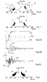
- FIG. 6 represents an incomplete set of zones 41, 42 of magnetic field magnitudes H X and H Y , the magnetic field H Y being positive, for which a systematic tilt of ⁇ 1 , initially oriented along the axis (OX) according to the X decreasing.
- the zones 41, 42 comprise "white" portions 43, 44 delimited by the solid lines which correspond to magnetic fields H X and H Y for which the standard of ⁇ tot , noted subsequently ⁇ tot , exceeds the standard of the vector magnetic moment ⁇ 1 , noted subsequently ⁇ 1 , at least at a time during the switchover of ⁇ 1 .
- the zones 41, 42 comprise black portions 45, 46 which correspond to magnetic fields H X and H Y for which ⁇ tot never exceeds ⁇ 1 during the switching of ⁇ 1 .
- FIG. 7 represents writing zones 47, 48, obtained from the zones 41, 42 of FIG. 5, and corresponding to values of the magnetic fields H X , H Y which impose a definite final orientation of ⁇ 1 regardless of the initial orientation. This is obtained by superimposing the zones 41 and 42 of FIG. 6 on zones corresponding to the symmetries of the zones 41, 42 with respect to the ordinate axis and retaining only the zones that are not common and for which ⁇ tot never exceeds ⁇ 1 .
- the magnetic fields H X and H Y associated with the writing zone 47 make it possible to ensure that ⁇ 1 is finally oriented according to the X increasing and the magnetic fields H X and H Y associated with the writing area 48 make it possible to ensure that ⁇ 1 is finally oriented according to the decreasing X's.
- the simulation uses the same parameters as those used to calculate Figures 6 and 7.
- the components are normed to ⁇ 1 , which is identical to ⁇ 2 , the norm of ⁇ 2 , for a compensated memory element.
- ⁇ 1 and ⁇ 2 are initially oriented along the axis (OX) respectively in the direction of the decreasing and increasing X's.
- ⁇ 1 rocker in less than 1 nanosecond after application of the magnetic field pulse H Y to orient along the axis (OX) in the direction of the X increasing.
- oscillations of smaller amplitude are observed for a few nanoseconds.
- the oscillations are very largely damped after 3 nanoseconds.
- the state of the memory element 16 is completely stabilized.
- the first embodiment of the write method according to the invention therefore makes it possible to achieve a write period of about 3 nanoseconds with the parameters used here for the calculation, out of any optimization.
- ⁇ tot remains very weak throughout the switchover of ⁇ 1 and, in particular, does not exceed at any time ⁇ 1 .
- ⁇ tot takes its maximum value only over a very short duration during the switchover of ⁇ 1 .
- the participation of ⁇ tot to perturbations of the memory elements adjacent to the memory element addressed because of dipolar interactions is very low.
- the short duration and small amplitudes of the magnetic fields H X and H Y make it possible to minimize the energy required for writing.
- the process direct write according to this first example of the invention is more favorable when it is the ferromagnetic layer more strong saturation magnetization that also has the strongest Planar effective anisotropy.
- the memory element 16 is then no longer a compensated structure but a structure that is almost compensated for.
- An increase in the area of the writing zones 49, 50 with respect to FIG. 7 is observed.
- the writing of the memory element can be carried out with magnetic fields H X and H Y whose amplitudes are smaller. to the respective amplitudes of the magnetic fields required for writing a compensated memory element.
- a decrease in the area of the writing areas 51, 52 with respect to FIG. 7 is observed. Such a modification of the compensation of the memory element is therefore not desirable.
- FIGS. 9 and 10 The physical origin of the differences between FIGS. 9 and 10 comes from the fact that, with the magnetic field values H X and H Y corresponding to the writing zones 47, 48 of FIG. ⁇ 2 who is the master vector and ⁇ 1 the slave vector in the writing process.
- a slight decompensation of the free magnetic region which reinforces the norm of the master vector (respectively slave) is favorable to the writing process (respectively unfavorable), in this sense. it decreases (respectively increases) the fields H X and H Y necessary for writing, and increases (respectively decreases) the extension of the field area H X and H Y allowing direct writing.
- a magnetic region 18 having two or more ferromagnetic layers gets more favorable writing ranges by choosing a almost compensated rather than compensated structure, achieved in stacking as in Figure 3 free magnetic regions 18, 18 ', 18 "almost compensated where the standard of vector magnetic moment acting as master vector during the writing process.
- the applicant has highlighted the presence of a range of magnetic fields writing amplitudes relatively moderates for writing a compensated memory element, and described the method for optimizing location and extent of this beach by playing on the dissymmetry of properties of the free magnetic region of the memory element.
- the plaintiff has shown that one can decrease the amplitude of the magnetic fields that can be used to writing a memory element by choosing a structure almost completely compensated.
- the second exemplary embodiment of the method for writing a memory element according to the present invention is based on the use of the reaction difference of the magnetic moment vectors. ⁇ 1 and ⁇ 2 when applying a magnetic field (of slow rise time with respect to the establishment of a precessional mode), when there is a difference in the effective planar anisotropy fields of the ferromagnetic layers of the magnetic region free of the memory element.
- the anisotropy field H A1 of the ferromagnetic layer 26 adjacent to the barrier layer 20 is larger than the anisotropy field H A2 the other ferromagnetic layer 28.
- the anisotropic field of FIG. a ferromagnetic layer whose associated magnetic moment vector is oriented as the magnetic moment vector associated with the ferromagnetic layer adjacent to the barrier layer is larger than the anisotropy field of any ferromagnetic layer whose magnetic moment vector is oriented in the opposite direction to that of the magnetic moment vector associated with the layer ferromagnetic adjacent to the barrier layer.
- FIGS. 11A to 11C illustrate successive steps of the writing of a memory element 16 according to the invention by the second embodiment of the writing method of applying a magnetic field H X alone, the magnetic field H Y being kept at zero.
- Figure 11A schematically shows the orientation of ⁇ 1 and ⁇ 2 before the application of the magnetic field H X.
- ⁇ 1 is initially oriented along the axis (OX) according to the X increasing and
- ⁇ 2 is initially oriented along the axis (OX) according to the X decreasing.
- the same magnetic properties values of the layers are used for the example as for FIGS.
- ⁇ 1 the angle formed by ⁇ 1 and the axis (OX)
- ⁇ 2 the angle formed by ⁇ 2 and the axis (OX).
- Figure 11C schematically shows the orientation of ⁇ 1 and ⁇ 2 after failover.
- ⁇ 1 is oriented along the axis (OX) according to the decreasing X's and
- ⁇ 2 is oriented along the axis (OX) according to the X increasing.
- FIGS. 12A to 12C depict figures similar to FIGS. 11A to 11C when a positive H X magnetic field is applied to memory element 16.
- Figure 12A is identical to Figure 11A.
- an angle ⁇ 1 of approximately + 48 ° and an angle ⁇ 2 of approximately -61 ° is also possible with the same magnetic energy and therefore the same probability.
- ⁇ 1 realigns along the axis (OX) according to the X increasing.
- ⁇ 2 is then returned along the axis (OX) according to the X decreasing under the effect of the antiferromagnetic interaction.
- Figure 12C identical to Figure 12A.
- the memory element according to the invention makes it possible to obtain a direct write with the application of a single magnetic field H X.
- a magnetic field H Y only whose absolute value is about 1591 A / m ( 20 Oe) is not enough to tip ⁇ 1 and ⁇ 2 , and since the absolute value of the tilting magnetic field H X is lowered when magnetic fields H X and H Y are simultaneously applied, it is possible to use a pair of magnetic fields H X and H Y to write directly. information in a single memory element 16 without changing the state of the memory elements which are only addressed by one or other of the magnetic fields H X or H Y.
- FIG. 13 represents, by way of example, the positions of ⁇ 1 and ⁇ 2 , in a manner analogous to FIG. 11B and starting from the configuration of FIG. 11A, in the case where a negative magnetic field H X and a positive magnetic field H Y are applied.
- a negative magnetic field H X and a positive magnetic field H Y are applied.
- ⁇ 1 equal to about 115 °
- ⁇ 2 equal to about -108 °.
- Figures 14A and 14B each represent the orientation of ⁇ 1 and ⁇ 2 , in a similar manner to FIG. 11B and starting from the configuration of FIG. 11A, in the case where only a negative magnetic field H X is applied and in the case where the free magnetic region 18 comprises a slight asymmetry of the compensation magnetic moment vectors.
- Figures 15A and 15B each represent the orientation of ⁇ 1 and ⁇ 2 , in a similar manner to FIG. 13, in the case where a negative magnetic field H X and a positive magnetic field H Y are applied simultaneously and in the case where the free magnetic region 18 of the memory element 16 comprises a slight asymmetry of the compensation of the magnetic moment vectors.
- ⁇ 1 is equal to approximately 212 °
- ⁇ 2 is equal to approximately 57 °.
- ⁇ 2 then turned an angle greater than 180 °.
- ⁇ tot is equal to approximately 0, 46 ⁇ 2 .
- Such a memory element is particularly advantageous insofar as when the magnetic field H Y is zero, the minimum amplitude of the writing magnetic field H X is greater than 150 Oe. In addition, ⁇ tot remains relatively low. There is then a significant difference in minimum amplitude of magnetic field H X writing, while maintaining relatively moderate amplitudes. This is favorable in particular to avoid unwanted writing of memory elements other than the addressed memory element.
- ⁇ 1 is equal to about 188 °
- ⁇ 2 is equal to about 25 °.
- ⁇ 2 then turned an angle greater than 180 °. ⁇ tot remains almost constant during the switchover and substantially equal to 0.46 ⁇ 2 .
- a decompensation of the free magnetic region 18 of the memory element 16 of increasing the standard of the magnetic moment vector associated with the strongest planar effective anisotropy field makes it possible to reduce the minimum amplitude of the magnetic field H X to apply for writing the memory element.
- the choice of a larger planar effective anisotropy for the layer 26 adjacent to the barrier layer 20 ensures that the magnetic moment vector ⁇ 1 of layer 26 acts as a master vector in the writing process. Due to the symmetry of the magnetism equations, the same direct writing method (only one must change the sign of H X ) can be achieved by giving a greater planar effective anisotropy to layer 28, the magnetic moment vector ⁇ 2 of this layer 28 then acting as a master vector in the writing process, and the antiferromagnetic coupling between the layers 26 and 28 through the layer 24 guaranteeing the final alignment of the magnetic moment vector ⁇ 1 .
- this second exemplary embodiment of the writing method according to the invention makes it possible, by applying a static field of components H X and H Y adapted, uniform or quasi-uniform over an entire MRAM memory, to give the same orientation to all free magnetic regions of all memory elements of the network.
- a field can easily be created by sources outside the circuit (magnet, electromagnet).
- Such an action may be useful for example to initialize or reset the operation of a memory, for example at the end of its manufacture, or to quickly erase all of an MRAM when the security of information depends on it.
- This last initialization method is also applicable in the same way as an MRAM defined in sense of the first embodiment of the writing method according to the invention, provided that there is a difference of field effective planar anisotropy of the ferromagnetic layers of the free magnetic region of the compensated memory element or almost compensated.
Landscapes
- Engineering & Computer Science (AREA)
- Computer Hardware Design (AREA)
- Mram Or Spin Memory Techniques (AREA)
- Hall/Mr Elements (AREA)
Abstract
Description
- les champs d'anisotropie d'origine cristallographique ;
- les tenseurs de champ démagnétisant.
- en prévoyant des couches ferromagnétiques composées de matériaux différents ;
- en prévoyant des couches ayant subi des traitements différents pour stabiliser des structures cristallographiques différentes, notamment par des conditions de dépôt, des recuits sous champ magnétique ou des implantations d'ions.
- les couches ferromagnétiques 26, 28 sont constituées de deux matériaux ferromagnétiques différents ayant des aimantations à saturation différentes ;
- les couches ferromagnétiques 26, 28 ont des sections droites différentes dans un plan perpendiculaire à la direction de l'empilement.
- l'empilement démarre au contact de la couche barrière 20 par une première région magnétique libre compensée ou quasiment compensée 18 ;
- au dessus d'une première couche de séparation 36 recouvrant la première région magnétique libre 18, on prévoit une deuxième région magnétique libre 18' qui doit être la symétrique de la première région magnétique libre 18 par rapport au plan médian de la couche de séparation 36 ;
- au dessus d'une deuxième couche de séparation 36' recouvrant la deuxième région magnétique libre 18', on prévoit une troisième région magnétique libre 18" qui doit être la symétrique de la deuxième région magnétique libre 18' par rapport au plan médian de la deuxième couche de séparation 36', c'est-à-dire que l'on retrouve ici la région magnétique libre 18 ;
- et ainsi de suite selon le besoin, de façon que ce soit toujours le même type de couche ferromagnétique (26 ou 28) qui se trouve de part et d'autre d'une couche de séparation 36, 36', etc ;
- les couches de séparation 36, 36', etc, induisent un couplage ferromagnétique fort entre les couches ferromagnétiques qu'elles séparent, gardant ainsi parallèles leurs vecteurs moment magnétique.
- réduire l'anisotropie effective globale de chaque région magnétique libre 18, 18', 18" etc., ce qui permet de réduire l'amplitude des champs magnétiques d'écriture,
- réduire les dimensions latérales d'un élément de mémoire vive magnétique sans avoir à augmenter son anisotropie magnétique totale.
- les couches ferromagnétiques 26, 28 sont constituées de deux matériaux ferromagnétiques différents ayant des aimantations à saturation différentes ;
- les couches ferromagnétiques 26, 28 ont des anisotropies de forme différentes, ce qui peut s'obtenir par une différence de section droite des couches dans un plan perpendiculaire à la direction d'empilement, ou par des épaisseurs différentes ;
- les couches ferromagnétiques 26, 28 ont des anisotropies magnétiques de nature cristallographique différente.
Claims (10)
- Elément mémoire magnétorésistif (16) comprenant une région magnétique piégée (22) et une région magnétique libre (18) séparées par une couche barrière (20), la région magnétique libre comprenant un empilement d'au moins deux couches ferromagnétiques (26, 28) couplées antiferromagnétiquement, à chaque couche étant associé un vecteur moment magnétique de couche (
µ 1,µ 2), le vecteur moment magnétique résultant, égal à la somme des vecteurs moment magnétique de couche, ayant une amplitude inférieure à au moins 40% de l'amplitude du vecteur moment magnétique de couche d'amplitude maximale, dans lequel le champ d'anisotropie et/ou le tenseur de champ démagnétisant n'est pas identique pour les au moins deux couches ferromagnétiques d'où il résulte que les déviations angulaires (1, 2) des vecteurs moment magnétique de couche sont différentes au moment de l'application d'un champ magnétique extérieur (HX, HY). - Elément mémoire magnétorésistif selon la revendication 1, dans lequel la région magnétique libre comprend un empilement d'au moins deux paires de couches ferromagnétiques (26, 28) couplées antiferromagnétiquement, à chaque couche ferromagnétique étant associé un vecteur moment magnétique de couche (
µ 1,µ 2), le vecteur moment magnétique résultant de chaque paire de couches, égal à la somme des vecteurs moment magnétique des couches ferromagnétiques de la paire de couches ferromagnétiques, ayant une amplitude inférieure à au moins 40% de l'amplitude du vecteur moment magnétique de couche d'amplitude maximale, les couches ferromagnétiques adjacentes des deux paires de couches ferromagnétiques étant couplées ferromagnétiquement, et dans lequel le champ d'anisotropie et/ou le tenseur de champ démagnétisant n'est pas identique pour les deux couches ferromagnétiques d'au moins une paire de couches ferromagnétiques, la disposition et les propriétés des couches ferromagnétiques dans chaque paire de couches ferromagnétiques étant adaptées pour que les vecteurs moment magnétique de couche (µ 1,µ 2) de deux couches ferromagnétiques adjacentes ferromagnétiquement couplées acquièrent des déviations angulaires (1, 2) identiques au moment de l'application d'un champ magnétique extérieur (HX, HY). - Elément mémoire magnétorésistif selon la revendication 1, dans lequel la région magnétique libre comprend un empilement d'au moins une première, une deuxième et une troisième couches ferromagnétiques (26, 28), les première et deuxième couches ferromagnétiques étant couplées antiferromagnétiquement, les deuxième et troisième couches ferromagnétiques étant couplées antiferromagnétiquement, à chacune des première, deuxième et troisième couches ferromagnétiques étant associé un vecteur moment magnétique de couche (
µ 1 ,µ 2), le vecteur moment magnétique résultant, égal à la somme des vecteurs moment magnétique de couche des première, deuxième et troisième couches ferromagnétiques, ayant une amplitude inférieure à au moins 40% de l'amplitude du vecteur moment magnétique de la deuxième couche ferromagnétique et dans lequel les champs d'anisotropie et/ou les tenseurs de champ démagnétisant de la première ou troisième couche ferromagnétique et de la deuxième couche ferromagnétique sont différents d'où il résulte que les déviations angulaires des vecteurs moment magnétique de couche des première et troisième couches ferromagnétiques sont identiques et différents de la déviation angulaire de la deuxième couche ferromagnétique au moment de l'application d'un champ magnétique extérieur (HX, HY). - Procédé d'écriture dans un élément mémoire (16) selon l'une quelconque des revendications 1 à 3, dans lequel le vecteur moment magnétique (
µ 1) de la couche ferromagnétique (26) de la région magnétique libre (18) en contact avec la couche barrière (20) est orienté selon l'une des deux orientations opposées d'une direction privilégiée (OX), comprenant, de façon au moins partiellement simultanée, les étapes suivantes :appliquer un premier champ magnétique (HX) selon la direction privilégiée ; etappliquer un second champ magnétique (HY) selon une direction (OY) sensiblement perpendiculaire à la direction privilégiée. - Procédé selon la revendication 4, dans lequel le tenseur de champ démagnétisant et/ou le champ d'anisotropie d'origine cristallographique n'est pas identique pour les au moins deux couches ferromagnétiques (26, 28), et dans lequel le second champ magnétique (HY) est appliqué, pendant l'application du premier champ magnétique (HX), sous la forme d'une impulsion dont le temps de montée est inférieur à la moitié de la période de précession la plus faible des au moins deux couches ferromagnétiques.
- Procédé selon la revendication 4, dans lequel les champs d'anisotropie effectifs planaires des au moins deux couches ferromagnétiques (26, 28) couplées antiferromagnétiquement ont des amplitudes différentes et dans lequel les premier et second champs magnétiques (HX, HY) sont appliqués simultanément pendant une durée supérieure aux temps de relaxation des vecteurs moment magnétique de couche (
µ 1,µ 2) des au moins deux couches ferromagnétiques (26, 28) couplées antiferromagnétiquement de la région magnétique libre (18) vers des positions d'équilibre respectives déterminées. - Procédé selon la revendication 6, dans lequel l'amplitude du second champ magnétique (HY) est inférieure à la moitié de l'amplitude du premier champ magnétique (HX).
- Procédé selon la revendication 6, dans lequel les instants de mise en place et/ou les durées d'application des premier et second champs magnétiques (HX, HY) sont différents.
- Procédé selon la revendication 6, dans lequel les premier et second champs magnétiques (HX, HY) sont appliqués de manière globale à une mémoire (10) constituée d'éléments mémoire (16) selon l'une quelconque des revendications 1 à 3, en utilisant une source de champ magnétique extérieure à la mémoire, d'où il résulte l'initialisation de la mémoire.
- Procédé selon la revendication 6, dans lequel les premier et second champs magnétiques (HX, HY) sont appliqués de manière globale à une mémoire (10) constituée d'éléments mémoire (16) selon l'une quelconque des revendications 1 à 3, en utilisant une source de champ magnétique extérieure à la mémoire, d'où il résulte l'effacement complet de la mémoire.
Applications Claiming Priority (2)
| Application Number | Priority Date | Filing Date | Title |
|---|---|---|---|
| FR0450779A FR2869445B1 (fr) | 2004-04-26 | 2004-04-26 | Element de memoire vive magnetique |
| FR0450779 | 2004-04-26 |
Publications (1)
| Publication Number | Publication Date |
|---|---|
| EP1592023A1 true EP1592023A1 (fr) | 2005-11-02 |
Family
ID=34939460
Family Applications (1)
| Application Number | Title | Priority Date | Filing Date |
|---|---|---|---|
| EP05103286A Withdrawn EP1592023A1 (fr) | 2004-04-26 | 2005-04-22 | Elément de mémoire vive magnétique |
Country Status (3)
| Country | Link |
|---|---|
| US (1) | US7298643B2 (fr) |
| EP (1) | EP1592023A1 (fr) |
| FR (1) | FR2869445B1 (fr) |
Families Citing this family (8)
| Publication number | Priority date | Publication date | Assignee | Title |
|---|---|---|---|---|
| US7502248B2 (en) * | 2004-05-21 | 2009-03-10 | Samsung Electronics Co., Ltd. | Multi-bit magnetic random access memory device |
| JP5077802B2 (ja) * | 2005-02-16 | 2012-11-21 | 日本電気株式会社 | 積層強磁性構造体、及び、mtj素子 |
| JP4877575B2 (ja) * | 2005-05-19 | 2012-02-15 | 日本電気株式会社 | 磁気ランダムアクセスメモリ |
| US7368301B2 (en) * | 2006-01-27 | 2008-05-06 | Magic Technologies, Inc. | Magnetic random access memory with selective toggle memory cells |
| TWI320930B (en) * | 2007-01-29 | 2010-02-21 | Ind Tech Res Inst | Direct writing method on magnetic memory cell and magetic memory cell structure |
| US20090027948A1 (en) * | 2007-07-24 | 2009-01-29 | Manfred Ruehrig | Integrated Circuits, Method of Programming a Cell, Thermal Select Magnetoresistive Element, Memory Module |
| US7532506B2 (en) * | 2007-09-17 | 2009-05-12 | Qimonda Ag | Integrated circuit, cell arrangement, method of operating an integrated circuit, memory module |
| KR102433703B1 (ko) * | 2015-11-30 | 2022-08-19 | 에스케이하이닉스 주식회사 | 전자 장치 |
Citations (2)
| Publication number | Priority date | Publication date | Assignee | Title |
|---|---|---|---|---|
| US5953248A (en) * | 1998-07-20 | 1999-09-14 | Motorola, Inc. | Low switching field magnetic tunneling junction for high density arrays |
| US20030072174A1 (en) * | 2001-10-16 | 2003-04-17 | Leonid Savtchenko | Method of writing to scalable magnetoresistance random access memory element |
Family Cites Families (6)
| Publication number | Priority date | Publication date | Assignee | Title |
|---|---|---|---|---|
| US6021065A (en) * | 1996-09-06 | 2000-02-01 | Nonvolatile Electronics Incorporated | Spin dependent tunneling memory |
| US6674664B2 (en) * | 2001-05-07 | 2004-01-06 | Nve Corporation | Circuit selected joint magnetoresistive junction tunneling-giant magnetoresistive effects memory cells |
| US6777730B2 (en) | 2001-08-31 | 2004-08-17 | Nve Corporation | Antiparallel magnetoresistive memory cells |
| US6633498B1 (en) * | 2002-06-18 | 2003-10-14 | Motorola, Inc. | Magnetoresistive random access memory with reduced switching field |
| US7095646B2 (en) * | 2002-07-17 | 2006-08-22 | Freescale Semiconductor, Inc. | Multi-state magnetoresistance random access cell with improved memory storage density |
| US6956764B2 (en) * | 2003-08-25 | 2005-10-18 | Freescale Semiconductor, Inc. | Method of writing to a multi-state magnetic random access memory cell |
-
2004
- 2004-04-26 FR FR0450779A patent/FR2869445B1/fr not_active Expired - Fee Related
-
2005
- 2005-04-22 EP EP05103286A patent/EP1592023A1/fr not_active Withdrawn
- 2005-04-25 US US11/114,305 patent/US7298643B2/en not_active Expired - Lifetime
Patent Citations (2)
| Publication number | Priority date | Publication date | Assignee | Title |
|---|---|---|---|---|
| US5953248A (en) * | 1998-07-20 | 1999-09-14 | Motorola, Inc. | Low switching field magnetic tunneling junction for high density arrays |
| US20030072174A1 (en) * | 2001-10-16 | 2003-04-17 | Leonid Savtchenko | Method of writing to scalable magnetoresistance random access memory element |
Also Published As
| Publication number | Publication date |
|---|---|
| US7298643B2 (en) | 2007-11-20 |
| FR2869445B1 (fr) | 2006-07-07 |
| FR2869445A1 (fr) | 2005-10-28 |
| US20050237796A1 (en) | 2005-10-27 |
Similar Documents
| Publication | Publication Date | Title |
|---|---|---|
| EP2073210B1 (fr) | Mémoire magnétique à écriture assistée thermiquement | |
| EP2436035B1 (fr) | Dispositif de memoire magnetique a polarisation de spin et son procede d'utilisation | |
| EP1808862B1 (fr) | Dispositif magnétique à jonction tunnel magnétique, mémoire et procédés d'écriture et de lecture utilisant ce dispositif | |
| EP2583281B1 (fr) | Mémoire magnétoélectrique | |
| WO2005086171A1 (fr) | Memoire magnetique a jonction tunnel magnetique a ecriture assistee thermiquement et procede pour son ecriture | |
| EP3026721B1 (fr) | Dispositif magnétique à polarisation de spin | |
| FR2904724A1 (fr) | Dispositif magnetique en couches minces a forte polarisation en spin perpendiculaire au plan des couches, jonction tunnel magnetique et vanne de spin mettant en oeuvre un tel dispositif | |
| EP3531432B1 (fr) | Jonction tunnel magnetique a anisotropie de forme perpendiculaire et variation en temperature minimisee, point memoire et element logique comprenant la jonction tunnel magnetique, procede de fabrication de la jonction tunnel magnetique | |
| FR2963153A1 (fr) | Element magnetique inscriptible | |
| FR2892231A1 (fr) | Dispositif magnetique a jonction tunnel magnetoresistive et memoire magnetique a acces aleatoire | |
| FR2931011A1 (fr) | Element magnetique a ecriture assistee thermiquement | |
| FR3009421A1 (fr) | Cellule memoire non volatile | |
| EP3531420B1 (fr) | Jonction tunnel magnetique a anisotropie de forme perpendiculaire et variabilite minimisee, point memoire et element logique comprenant la jonction tunnel magnetique, procede de fabrication de la jonction tunnel magnetique | |
| FR2989211A1 (fr) | Dispositif magnetique a ecriture assistee thermiquement | |
| FR2882459A1 (fr) | Element de memoire magnetoresistive presentant une structure empilee. | |
| EP1592023A1 (fr) | Elément de mémoire vive magnétique | |
| EP2685458B1 (fr) | Dispositif magnétique à écriture assistée thermiquement | |
| FR2944910A1 (fr) | Dispositif de memorisation magnetique a vortex | |
| EP2681739B1 (fr) | Dispositif magnetique et procede d'ecriture et de lecture d'une information stockee dans un tel dispositif magnetique | |
| FR2938369A1 (fr) | Procede de fabrication d'une couche d'un materiau antiferromagnetique a structures magnetiques controlees | |
| Peng et al. | Single laser pulse switching in RE-based multilayers without Gd | |
| EP4044185A1 (fr) | Dispositif magnétique cryogénique plus particulièrement pour mémoire ou composant logique | |
| FR2846459A1 (fr) | Procede de realisation d'une nanostructure magnetique ayant des performances dynamiques ameliorees, nanostructure et memoires magnetiques obtenues et procedes de retournement de leur aimantation. |
Legal Events
| Date | Code | Title | Description |
|---|---|---|---|
| PUAI | Public reference made under article 153(3) epc to a published international application that has entered the european phase |
Free format text: ORIGINAL CODE: 0009012 |
|
| AK | Designated contracting states |
Kind code of ref document: A1 Designated state(s): AT BE BG CH CY CZ DE DK EE ES FI FR GB GR HU IE IS IT LI LT LU MC NL PL PT RO SE SI SK TR |
|
| AX | Request for extension of the european patent |
Extension state: AL BA HR LV MK YU |
|
| 17P | Request for examination filed |
Effective date: 20060421 |
|
| RIN1 | Information on inventor provided before grant (corrected) |
Inventor name: FOURNEL, RICHARD Inventor name: MAUFRONT, CEDRIC Inventor name: CHAPPERT, CLAUDE Inventor name: DEVOLDER, THIBAUT Inventor name: KIM, JOO-VON |
|
| AKX | Designation fees paid |
Designated state(s): DE FR GB IT |
|
| STAA | Information on the status of an ep patent application or granted ep patent |
Free format text: STATUS: THE APPLICATION IS DEEMED TO BE WITHDRAWN |
|
| 18D | Application deemed to be withdrawn |
Effective date: 20121101 |