EP1591792A2 - Beschleunigungssensor mit Kompensation für externe Magnetfelder - Google Patents
Beschleunigungssensor mit Kompensation für externe Magnetfelder Download PDFInfo
- Publication number
- EP1591792A2 EP1591792A2 EP05009085A EP05009085A EP1591792A2 EP 1591792 A2 EP1591792 A2 EP 1591792A2 EP 05009085 A EP05009085 A EP 05009085A EP 05009085 A EP05009085 A EP 05009085A EP 1591792 A2 EP1591792 A2 EP 1591792A2
- Authority
- EP
- European Patent Office
- Prior art keywords
- cantilever
- magnetic field
- magnetic
- accelerometer
- detecting
- Prior art date
- Legal status (The legal status is an assumption and is not a legal conclusion. Google has not performed a legal analysis and makes no representation as to the accuracy of the status listed.)
- Withdrawn
Links
- 230000002093 peripheral effect Effects 0.000 claims abstract description 106
- 238000001514 detection method Methods 0.000 claims abstract description 35
- 238000006073 displacement reaction Methods 0.000 claims abstract description 29
- 229910018104 Ni-P Inorganic materials 0.000 claims abstract description 10
- 229910018536 Ni—P Inorganic materials 0.000 claims abstract description 10
- 229910045601 alloy Inorganic materials 0.000 claims abstract description 8
- 239000000956 alloy Substances 0.000 claims abstract description 8
- 230000001133 acceleration Effects 0.000 claims description 88
- 229910052751 metal Inorganic materials 0.000 claims description 41
- 239000002184 metal Substances 0.000 claims description 41
- 230000008859 change Effects 0.000 claims description 30
- 229920005989 resin Polymers 0.000 claims description 25
- 239000011347 resin Substances 0.000 claims description 25
- 230000001965 increasing effect Effects 0.000 claims description 17
- 239000000758 substrate Substances 0.000 claims description 16
- 230000001939 inductive effect Effects 0.000 claims description 15
- 238000002161 passivation Methods 0.000 claims description 13
- 230000003247 decreasing effect Effects 0.000 claims description 12
- 230000035945 sensitivity Effects 0.000 claims description 10
- 229910052804 chromium Inorganic materials 0.000 claims description 7
- 229910052719 titanium Inorganic materials 0.000 claims description 7
- 229910052782 aluminium Inorganic materials 0.000 claims description 6
- 239000000919 ceramic Substances 0.000 claims description 4
- 229910052802 copper Inorganic materials 0.000 claims description 4
- 229910052737 gold Inorganic materials 0.000 claims description 4
- 229910052725 zinc Inorganic materials 0.000 claims description 4
- 230000008093 supporting effect Effects 0.000 claims description 3
- 239000004020 conductor Substances 0.000 claims description 2
- 238000005259 measurement Methods 0.000 abstract description 5
- 239000010410 layer Substances 0.000 description 72
- 238000000034 method Methods 0.000 description 17
- 230000000694 effects Effects 0.000 description 16
- 239000010408 film Substances 0.000 description 12
- 230000001976 improved effect Effects 0.000 description 12
- 230000005415 magnetization Effects 0.000 description 11
- 239000000463 material Substances 0.000 description 9
- 238000004519 manufacturing process Methods 0.000 description 8
- 230000005489 elastic deformation Effects 0.000 description 6
- 230000003014 reinforcing effect Effects 0.000 description 6
- 238000004544 sputter deposition Methods 0.000 description 5
- QVGXLLKOCUKJST-UHFFFAOYSA-N atomic oxygen Chemical compound [O] QVGXLLKOCUKJST-UHFFFAOYSA-N 0.000 description 4
- 125000000524 functional group Chemical group 0.000 description 4
- 125000002887 hydroxy group Chemical group [H]O* 0.000 description 4
- 239000000696 magnetic material Substances 0.000 description 4
- 229910052760 oxygen Inorganic materials 0.000 description 4
- 239000001301 oxygen Substances 0.000 description 4
- 230000008569 process Effects 0.000 description 4
- 230000001360 synchronised effect Effects 0.000 description 4
- 239000003990 capacitor Substances 0.000 description 3
- 238000010586 diagram Methods 0.000 description 3
- 239000003822 epoxy resin Substances 0.000 description 3
- 230000005389 magnetism Effects 0.000 description 3
- 238000007747 plating Methods 0.000 description 3
- 229920000647 polyepoxide Polymers 0.000 description 3
- 229910052709 silver Inorganic materials 0.000 description 3
- 239000010409 thin film Substances 0.000 description 3
- 238000005530 etching Methods 0.000 description 2
- 230000006870 function Effects 0.000 description 2
- 238000010438 heat treatment Methods 0.000 description 2
- 239000000203 mixture Substances 0.000 description 2
- 239000003973 paint Substances 0.000 description 2
- 238000005240 physical vapour deposition Methods 0.000 description 2
- 230000009467 reduction Effects 0.000 description 2
- 239000000126 substance Substances 0.000 description 2
- 229910000859 α-Fe Inorganic materials 0.000 description 2
- 239000004593 Epoxy Substances 0.000 description 1
- 229910001030 Iron–nickel alloy Inorganic materials 0.000 description 1
- XUIMIQQOPSSXEZ-UHFFFAOYSA-N Silicon Chemical compound [Si] XUIMIQQOPSSXEZ-UHFFFAOYSA-N 0.000 description 1
- -1 SmFeN Inorganic materials 0.000 description 1
- 230000002411 adverse Effects 0.000 description 1
- 229910000828 alnico Inorganic materials 0.000 description 1
- 238000007598 dipping method Methods 0.000 description 1
- 238000001035 drying Methods 0.000 description 1
- 230000004907 flux Effects 0.000 description 1
- 230000007274 generation of a signal involved in cell-cell signaling Effects 0.000 description 1
- 239000011810 insulating material Substances 0.000 description 1
- 150000002739 metals Chemical class 0.000 description 1
- 229910001172 neodymium magnet Inorganic materials 0.000 description 1
- 239000005011 phenolic resin Substances 0.000 description 1
- 229920006122 polyamide resin Polymers 0.000 description 1
- 229910052761 rare earth metal Inorganic materials 0.000 description 1
- 150000002910 rare earth metals Chemical class 0.000 description 1
- 229910000938 samarium–cobalt magnet Inorganic materials 0.000 description 1
- 229910052710 silicon Inorganic materials 0.000 description 1
- 239000010703 silicon Substances 0.000 description 1
- 239000002356 single layer Substances 0.000 description 1
- 238000005476 soldering Methods 0.000 description 1
- 229920005992 thermoplastic resin Polymers 0.000 description 1
- 229920001187 thermosetting polymer Polymers 0.000 description 1
- 238000007740 vapor deposition Methods 0.000 description 1
Images


Classifications
-
- G—PHYSICS
- G01—MEASURING; TESTING
- G01P—MEASURING LINEAR OR ANGULAR SPEED, ACCELERATION, DECELERATION, OR SHOCK; INDICATING PRESENCE, ABSENCE, OR DIRECTION, OF MOVEMENT
- G01P1/00—Details of instruments
- G01P1/006—Details of instruments used for thermal compensation
-
- E—FIXED CONSTRUCTIONS
- E05—LOCKS; KEYS; WINDOW OR DOOR FITTINGS; SAFES
- E05B—LOCKS; ACCESSORIES THEREFOR; HANDCUFFS
- E05B17/00—Accessories in connection with locks
- E05B17/14—Closures or guards for keyholes
- E05B17/18—Closures or guards for keyholes shaped as lids or slides
-
- G—PHYSICS
- G01—MEASURING; TESTING
- G01P—MEASURING LINEAR OR ANGULAR SPEED, ACCELERATION, DECELERATION, OR SHOCK; INDICATING PRESENCE, ABSENCE, OR DIRECTION, OF MOVEMENT
- G01P1/00—Details of instruments
- G01P1/02—Housings
- G01P1/023—Housings for acceleration measuring devices
-
- G—PHYSICS
- G01—MEASURING; TESTING
- G01P—MEASURING LINEAR OR ANGULAR SPEED, ACCELERATION, DECELERATION, OR SHOCK; INDICATING PRESENCE, ABSENCE, OR DIRECTION, OF MOVEMENT
- G01P15/00—Measuring acceleration; Measuring deceleration; Measuring shock, i.e. sudden change of acceleration
- G01P15/02—Measuring acceleration; Measuring deceleration; Measuring shock, i.e. sudden change of acceleration by making use of inertia forces using solid seismic masses
- G01P15/08—Measuring acceleration; Measuring deceleration; Measuring shock, i.e. sudden change of acceleration by making use of inertia forces using solid seismic masses with conversion into electric or magnetic values
- G01P15/105—Measuring acceleration; Measuring deceleration; Measuring shock, i.e. sudden change of acceleration by making use of inertia forces using solid seismic masses with conversion into electric or magnetic values by magnetically sensitive devices
-
- G—PHYSICS
- G01—MEASURING; TESTING
- G01P—MEASURING LINEAR OR ANGULAR SPEED, ACCELERATION, DECELERATION, OR SHOCK; INDICATING PRESENCE, ABSENCE, OR DIRECTION, OF MOVEMENT
- G01P15/00—Measuring acceleration; Measuring deceleration; Measuring shock, i.e. sudden change of acceleration
- G01P15/18—Measuring acceleration; Measuring deceleration; Measuring shock, i.e. sudden change of acceleration in two or more dimensions
-
- G—PHYSICS
- G01—MEASURING; TESTING
- G01P—MEASURING LINEAR OR ANGULAR SPEED, ACCELERATION, DECELERATION, OR SHOCK; INDICATING PRESENCE, ABSENCE, OR DIRECTION, OF MOVEMENT
- G01P15/00—Measuring acceleration; Measuring deceleration; Measuring shock, i.e. sudden change of acceleration
- G01P15/02—Measuring acceleration; Measuring deceleration; Measuring shock, i.e. sudden change of acceleration by making use of inertia forces using solid seismic masses
- G01P15/08—Measuring acceleration; Measuring deceleration; Measuring shock, i.e. sudden change of acceleration by making use of inertia forces using solid seismic masses with conversion into electric or magnetic values
- G01P2015/0805—Measuring acceleration; Measuring deceleration; Measuring shock, i.e. sudden change of acceleration by making use of inertia forces using solid seismic masses with conversion into electric or magnetic values being provided with a particular type of spring-mass-system for defining the displacement of a seismic mass due to an external acceleration
- G01P2015/0822—Measuring acceleration; Measuring deceleration; Measuring shock, i.e. sudden change of acceleration by making use of inertia forces using solid seismic masses with conversion into electric or magnetic values being provided with a particular type of spring-mass-system for defining the displacement of a seismic mass due to an external acceleration for defining out-of-plane movement of the mass
- G01P2015/0825—Measuring acceleration; Measuring deceleration; Measuring shock, i.e. sudden change of acceleration by making use of inertia forces using solid seismic masses with conversion into electric or magnetic values being provided with a particular type of spring-mass-system for defining the displacement of a seismic mass due to an external acceleration for defining out-of-plane movement of the mass for one single degree of freedom of movement of the mass
- G01P2015/0828—Measuring acceleration; Measuring deceleration; Measuring shock, i.e. sudden change of acceleration by making use of inertia forces using solid seismic masses with conversion into electric or magnetic values being provided with a particular type of spring-mass-system for defining the displacement of a seismic mass due to an external acceleration for defining out-of-plane movement of the mass for one single degree of freedom of movement of the mass the mass being of the paddle type being suspended at one of its longitudinal ends
Definitions
- the present invention relates to an accelerometer using magnetic sensors.
- an accelerometer for example, there may be mentioned a device formed of a magnet body to be displaced in accordance with acting acceleration and a magnetic sensor detecting the change in magnetic field generated by the above magnet body.
- This accelerometer measures the amount of displacement of the magnet body based on the change in magnetic field, that is, measures the magnitude of acting acceleration (see, e.g., see Patent Document 1).
- Patent Document 1 Japanese Unexamined Patent Application Publication No. 2000-258449
- the related accelerometer described above when a peripheral magnetic field, such as earth magnetism, is applied to the magnet body, this magnet body may behave as a compass and be displaced regardless of acting acceleration in some cases.
- a compact accelerometer formed in combination of a small magnet body and a low elastic cantilever may frequently cause the problem described above.
- the present invention was made in consideration of the problem described above, and an object of the present invention is to provide an accelerometer for measuring the displacement of a magnet body using a magnetic sensor, in which the accuracy of the accelerometer is improved by suppressing influence of a peripheral magnetic field.
- an accelerometer comprising: a substrate, at least one detecting unit, and at least one peripheral magnetic field detecting portion.
- the detecting unit has a support member erected on the substrate, a cantilever which is elastically deformed to rotate around a fixed end thereof fixed by the support member, a magnet body provided at a free end of the cantilever, and a magnetic detecting head portion provided outside the rotation region of the cantilever.
- the peripheral magnetic field detecting portion measures a peripheral magnetic field applied to the magnetic detecting head portion and the magnet body.
- the peripheral magnetic field detecting portion of the accelerometer of the present invention measures a peripheral magnetic field applied to the magnetic detecting head portion and the magnet body provided on the cantilever.
- the peripheral magnetic field detecting portion By this peripheral magnetic field detecting portion, the peripheral magnetic field directly applied to the magnetic detecting head portion can be detected.
- the peripheral magnetic field detecting portion of the detection signal output from the magnetic detecting head portion, an error component generated by the application of the peripheral magnetic field can be corrected.
- the peripheral magnetic field detecting portion the peripheral magnetic field applied to the magnet body to generate a torque therein and to elastically deform the cantilever can be detected.
- this peripheral magnetic field regardless of acceleration acting on the accelerometer described above, the amount of displacement of the magnet body caused by the influence of the peripheral magnetic field can be estimated.
- an error component resulting from the displacement of the magnet body caused by the torque can be estimated.
- an error component generated by the indirect influence of the' peripheral magnetic field via the displacement of the magnet body can be corrected.
- the error component by the direct influence of the peripheral magnetic field and the error component by the indirect influence thereof can be corrected, and hence the acting acceleration can be accurately measured.
- the torque generated in the magnet body described above is a rotational force generated when a magnetic field is applied to the magnet body which has a magnetic moment in a predetermined direction. This magnetic moment is the product of the magnetic pole intensity of the magnet body and the distance between the magnetic poles and has directionality.
- the torque is similar to a rotational force for rotating a compass needle and has directionality depending on the orientation of the magnetic moment.
- an acceleration sensing part comprising: a cantilever which is elastically deformed so as to rotate around a fixed end thereof; a magnet body provided at a free end of the cantilever; and a support member fixing and supporting the fixed end of the cantilever, in which acting acceleration is converted into the change in magnetic field caused by displacement of a magnet body.
- the support member has a base portion bonded to the fixed end and an extending portion extending from the base portion to the free end side of the cantilever, and a space is provided between the cantilever and the extending portion.
- the above acceleration sensing part converts acting acceleration into the change in magnetic field caused by the displacement of the magnet body. That is, the acceleration acting on the acceleration sensing part described above acts on the free end of the cantilever to which the magnet body is fixed. Accordingly, as the cantilever is elastically deformed and the free end thereof is displaced, the magnet body is displaced, and as a result, a magnetic field generated from the magnet body is changed. Hence, when being converted into the change in magnetic field, the acceleration can be sensed. When the change in magnetic field described above is detected by magnetic detecting means, the acceleration can be detected.
- the rigidity of the cantilever is decreased as much as possible so that the deformation can be more easily obtained. Accordingly, when the acceleration sensing part is handled, the cantilever which is easily deformed and the magnet body fixed to the free end of the cantilever must be prevented from being touched.
- the support member is composed of the base portion and the extending portion.
- the accelerometer according to the first aspect of the present invention may be widely used, for example, for measuring motion information of automobiles and autonomous mobile robots and for controlling manipulators of robot arms of stationary robots and the like.
- the accelerometer described above may be mounted on a portable device such as a personal digital assistant (PDA) or a mobile phone.
- PDA personal digital assistant
- the magnetic detecting head portion of the present invention may be formed using a magnetic sensing element such as a hall element, a magnetic impedance element, a magnetoresistance element, or a flux gate element.
- the magnet body described above may be formed using ferrite, a rare earth magnet, or the like.
- gravitational acceleration may also be mentioned.
- a sensing direction of the peripheral magnetic field detecting portion in which magnetic detection sensitivity is maximum is preferably parallel to a sensing direction of the magnetic detecting head portion in which magnetic detection sensitivity is maximum.
- a peripheral magnetic field component applied to the magnetic detecting head portion can be accurately detected using the peripheral magnetic field detecting portion.
- the amount of elastic deformation of the cantilever caused by a torque, which is generated in the magnet body due to the application of the peripheral magnetic field, and the amount of displacement of the magnet body caused by the elastic deformation described above can be accurately calculated.
- the two sensing directions described above may be substantially parallel to each other, and as long as the operational effect described above can be satisfactorily obtained, the directions described above may be in a state which is slightly deviated from a strictly parallel state.
- terms such as “parallel”, “orthogonal”, “uniform”, and “proportional” represent “substantially parallel”, “substantially orthogonal”, substantially uniform”, and “substantially proportional”, respectively, and are not intended to represent only the strict parallel state and the like.
- the magnetic detecting head portion and the peripheral magnetic field detecting portion each preferably comprise a magnetic sensing member and an electromagnetic coil coiled around the periphery of the magnetic sensing member to form a magneto-impedance (MI) element which generates a potential difference between the two ends of the electromagnetic coil in accordance with the change in current supplied to the magnetic sensing member.
- MI magneto-impedance
- a phenomenon in which an inductive voltage is generated in the electromagnetic coil in accordance with the change in current supplied to the magnetic sensing member is called a MI effect.
- This MI effect is generated in a magnetic sensing member having electron spin orientation in a circumferential direction with respect to the direction of a supply current.
- the MI element is an element using a magnetic sensing member formed of a magnetic material having electron spin orientation in a circumferential direction with respect to the direction of a supply current.
- a magnetic sensing member formed of a magnetic material having electron spin orientation in a circumferential direction with respect to the direction of a supply current.
- the current supplied to the magnetic sensing member is rapidly changed, a magnetic field in the circumferential direction is rapidly changed, and by this change in magnetic field, the change in electron spin direction occurs in accordance with the peripheral magnetic field.
- an element is formed so that the change in internal magnetization, impedance, or the like of the magnetic sensing member described above is converted, for example, into a voltage or a current generated in the magnetic sensing member or a voltage or a current generated between two ends of an electromagnetic coil disposed around the periphery of the magnetic sensing member, thereby obtaining the MI element.
- this MI element is combined with an electronic circuit, a so-called MI sensor is obtained.
- the magnetic detecting head portion described above is formed using an MI element in which a potential difference is generated between two ends of an electromagnetic coil in accordance with the change in current supplied to a magnetic sensing member as described above, highly sensitive magnetic detection can be performed, and the displacement of the magnet body can be accurately detected.
- a magnetic sensing member described above for example, a wire-shaped or a thin-film member may be used.
- a material for the magnetic sensing member for example, FeCoSiB and NiFe may be mentioned.
- the magnetic detecting head portion and the peripheral magnetic field detecting portion are each preferably formed to measure the intensity of an acting magnetic field by measuring an inductive voltage generated between the two ends of the electromagnetic coil when a current supplied to the magnetic sensing member is rapidly increased or decreased within 10 nanoseconds.
- the rapid change in supply current as described above in the magnetic sensing member described above, the change in magnetic field in the circumferential direction can be generated at a speed approximately equivalent to a propagation speed of the change in electron spin direction, and hence a sufficient MI effect can be obtained.
- the change in current containing a high frequency component of approximately 0.1 GHz is allowed to act on the magnetic sensing member.
- the inductive voltage generated between the two ends of the electromagnetic coil described above is measured, the change in internal magnetic field generated in the magnetic sensing member in accordance with the peripheral magnetic field can be measured as the inductive voltage, and in addition, the intensity of the peripheral magnetic field can be more accurately measured.
- the rapid increase of a supply current and the rapid decrease thereof indicate increase and decrease in current supplied to the above magnetic impedance element from 10% (90%) to 90% (10%) of a steady-state current, respectively.
- a practical lower limit of the time for the rapid increase and decrease is determined, for example, by the limitation of an apparatus or the like generating the supply current.
- the magnetic detecting head portion and the peripheral magnetic field detecting portion are each preferably formed to measure the inductive voltage generated between the two ends of the electromagnetic coil when the current supplied to the magnetic sensing member is rapidly decreased. Compared to the case in which the supply current is rapidly increased, when the supply current is rapidly decreased, the linearity of an output voltage from the magnetic detecting head portion with respect to the intensity of the magnetic field becomes superior.
- the number of said at least one detecting unit is preferably two so as to detect acceleration acting along two axis directions orthogonally intersecting each other. In this case, when the accelerometer described above is used, acceleration acting in an optional direction along a plane defined by the above two axes can be measured.
- the number of said at least one detecting unit is preferably three so as to detect acceleration acting along three axis directions orthogonally intersecting each other. In this case, when the accelerometer described above is used, acceleration acting in an optional direction can be measured.
- the accelerometer described above may further comprise an electrical circuit for controlling the magnetic detecting head portion and the peripheral magnetic field detecting portion.
- the accelerometer including the above electrical circuit can be miniaturized, and in addition, when the electrical circuit is modularized, the electrical power consumption of the accelerometer can be reduced.
- the above electrical circuit is preferably formed to receive a detection signal of the magnetic detecting head portion and a detection signal of the peripheral magnetic field detecting portion provided corresponding thereto so as to perform signal processing.
- the above electrical circuit is preferably formed to receive a detection signal of the magnetic detecting head portion and a detection signal of the peripheral magnetic field detecting portion provided corresponding thereto so as to perform signal processing.
- a method may be mentioned in which a detection signal of the magnetic detecting head portion and a detection signal of the peripheral magnetic field detecting portion are received in parallel and are then processed.
- the error component of the detection signal of the magnetic detecting head portion can be estimated.
- the correction can be made so as to improve the measurement accuracy of the accelerometer described above.
- a method may also be mentioned in which the magnetic detecting head portion and the peripheral magnetic field detecting portion are formed so as to output detection signals having opposite signs (positive and negative) to each other when the same peripheral magnetic field is applied thereto and are connected to each other in series.
- the ratio of the intensity of the detection signal of the peripheral magnetic field detecting portion to that of the magnetic detecting head portion is appropriately determined, a signal excluding the error component from the detection signal of the magnetic detecting head portion can be obtained.
- the peripheral magnetic field detecting portion may be connected to the magnetic detecting head portion in series.
- the accelerometer described above is preferably modularized.
- the rigidity thereof can be increased, and the measurement accuracy of the accelerometer can be improved.
- the relationship between the detecting units can be made similar to a rigid body.
- the accelerometer has higher measurement accuracy.
- the electrical power consumption of the accelerometer thus modularized can be reduced.
- the detecting unit may further comprise at least one stopper provided in the rotation direction of the free end of the cantilever in order to prevent excessive displacement thereof.
- the stopper may be provided at one side of the rotation direction of the free end of the cantilever or may be provided at both sides thereof.
- the stopper is preferably integrated with the support member described above. In this case, since the number of parts forming the accelerometer can be decreased, easy assembly properties and reduction in cost can be advantageously obtained.
- the acceleration sensing part in accordance with the second aspect of the present invention may be applied to the above accelerometer according to the first aspect of the present invention.
- an accelerometer having high accuracy can be obtained. That is, since the accelerometer according to the first aspect of the present invention is formed to improve the measurement accuracy by suppressing the influence of a peripheral magnetic field as described above, an acceleration sensing part to be used also must have a high sensing sensitivity.
- a cantilever which is likely to be deformed is used, and hence in handling thereof, the probability of the cantilever and the magnet body to be being touched must be made as small as possible. Accordingly, when the acceleration sensing part according to the second aspect of the present invention is used, the problem described above, which may frequently occur in handling an acceleration sensing part having a high sensing sensitivity, can be easily solved.
- the length of the support member is preferably larger than that of the cantilever. In this case, when the two ends of the support member in the longitudinal direction are held, the cantilever can be easily prevented from being touched.
- the cantilever described above is a conductor, that the support member have a conductive layer on a surface of the extending portion facing the cantilever, and that the conductive layer be electrically connected to the cantilever.
- the surface of the extending portion of the support member facing the cantilever can be prevented from being electrostatically charged, and hence the displacement of the cantilever caused by an electrostatic force can be prevented. Accordingly, an error caused by electrostatic charges can be prevented, and as a result, an accelerometer having a high accuracy can be obtained.
- the support member is made of an insulating material
- electrostatic charges may be generated on the facing surface of the cantilever and that of the extending portion of the support member so as to attract each other in some cases.
- a conductive layer electrically connected to the cantilever is formed on the facing surface of the extending portion of the support member, the cantilever and the facing surface of the extending portion of the support member have the same potential, and as a result, the generation of electrostatic charges can be prevented.
- the conductive layer is preferably connected to the ground of the electrical circuit formed on the substrate.
- the conductive layer is preferably formed on the entire facing surface; however, even when being provided on part thereof, the effect described above can also be obtained.
- the cantilever preferably comprises a Ni-P alloy.
- a cantilever can be formed having superior spring properties, such as a low elastic modulus, a wide elastic deformation region, and a high breaking strength. Accordingly, the amount of displacement of the cantilever caused by the same acceleration is increased, and as a result, the sensitivity of the acceleration sensing part is improved. In addition, a cantilever having a high detecting accuracy of acceleration and superior durability can be obtained.
- the support member preferably comprises a ceramic
- the acceleration sensing part may further comprise a multiple metal-layer having a plurality of metal layers between the support member and the fixed end of the cantilever.
- adhesion between the support member and the cantilever can be improved.
- the multiple metal-layer have a first metal layer provided adjacent to the support member and a second metal layer provided adjacent to the cantilever, that the first metal layer comprise at least one of Ti, Cr, and Al, and that the second metal layer comprise at least one of Cu, Au, and Ag.
- the bonding between the first metal layer and the support member and that between the second metal layer and the cantilever are ensured, and as a result, the adhesion between the support member and the cantilever can be further improved.
- the magnet body preferably comprises a resin magnet or comprises a magnet and a resin layer which is to be bonded to the cantilever, and the acceleration sensing part may further comprise a metal layer forming a stable passive film to be bonded to the magnet body.
- the passivation film and the resin have good affinity to each other, the adhesion between the cantilever and the magnet body can be improved. That is, since having reactive functional groups such as an oxygen-containing group and a hydroxyl group on the surface, the passivation film has good affinity to the resin.
- the reactive functional groups such as an oxygen-containing group and a hydroxyl group are uniformly present, and hence the affinity to the resin is further improved.
- the bonding between the cantilever and the magnet body can be improved.
- the magnet body described above is a sintered magnet
- a resin layer is provided on the surface thereof so as to be bonded to the cantilever as described above.
- the metal layer preferably comprises at least one of Cr, Al, Zn, and Ti. In this case, a particularly stable passivation film can be formed.
- an accelerometer 1 which uses an amorphous wire as a magnetic sensing member 24.
- the accelerator 1 of this embodiment includes detecting unit 2a (2b) having a cantilever 22 to be elastically deformed so as to rotate around a fixed end 221 thereof, a magnet body 21a (21b) provided at a free end 222 of the cantilever 22, and a magnetic detecting head portion 23a (23b) disposed outside the rotation region of the cantilever 22.
- this accelerometer 1 has peripheral magnetic field detecting portions 43a and 43b for measuring a peripheral magnetic field applied to the magnetic detecting head portions 23a and 23b and magnet bodies 21a and 21b.
- peripheral magnetic field detecting portions 43a and 43b for measuring a peripheral magnetic field applied to the magnetic detecting head portions 23a and 23b and magnet bodies 21a and 21b.
- the accelerometer 1 of this embodiment has the two detecting units 2a and 2b formed in combination of the cantilevers 22 and the magnetic detecting head portions 23a and 23b, the two peripheral magnetic field detecting portions 43a and 43b, and an IC chip 12 containing an electrical circuit functioning as a control circuit on a common IC substrate 10, and the components described above are integrated to produce a modularized form.
- the magnitude of an inertial force applied to the cantilever 22 in accordance with acting acceleration is converted into the amount of displacement of the magnet body 21a (21b) disposed at the free end 222. Subsequently, by the use of the magnetic detecting head portion 23a (23b), the amount of displacement of the magnet body 21a (21b) is detected, thereby measuring the magnitude of the acting acceleration.
- the structure is formed so as to detect acceleration acting along an X axis 10a direction and that along a Y axis 10b direction in accordance with the amounts of displacement of the magnet bodies 21b and 21a of the detecting units 2b and 2a, the X axis 10a and the Y axis 10b directions being defined along two orthogonal sides of the IC substrate 10.
- the cantilever 22 is formed of an elastic body having a cantilever shape and is supported at the fixed end 221 thereof, which is one end in the axis direction, by a support post 28 erected on the surface of the IC substrate 10.
- the magnet body 21a (21b) is provided at the free end 222 which is the other end of the cantilever 22 opposite to the side supported by the support post 28.
- the cantilever 22 of this embodiment is formed of NiP and has an approximately rectangular shape having a width of 0.3 mm, a length of 1.5 mm, and a thickness of 5 ⁇ m.
- a long hole 220 having a width of 0.22 mm is provided from a foot portion at the support post 28 side to a position of 0.38 mm from the free end 222.
- a sheet-shaped cantilever may also be formed.
- the characteristic frequency of the cantilever 22 is set to approximately 50 to 60 Hz.
- the characteristic frequency of the cantilever 22 is set in the range of 50 to 60 Hz, for example, an acceleration of 0 to 40 Hz generated by an automobile or the like can be accurately detected.
- the characteristic frequency is set to less than 50 Hz, an acceleration of approximately 40 Hz may not be accurately detected in some cases.
- the magnet body 21a (21b) is disposed on a side surface of the cantilever 22 in the vicinity of the free end 222 thereof.
- a magnetic paint is applied onto the side surface and is magnetized after drying and curing of the paint, thereby forming the magnet body 21.
- the magnet body 21 is formed to have a width (the dimension of the cantilever 22 in the axis direction) W of 0.5 mm, a height H of 0.3 mm, and a thickness T of 100 ⁇ m.
- the magnetic detecting head portion 23a (23b) is formed using an amorphous wire (hereinafter referred to as "amorphous wire 24" in some cases) having a length of 1 mm and a diameter of 20 ⁇ m as the magnetic sensing member 24.
- amorphous wire 24 amorphous wire 24
- the magnetic detecting head portion 23a (23b) is formed of the amorphous wire 24, a tube-shaped insulating resin 26 covering the wire 24, and an electromagnetic coil 25 having an internal diameter of 200 ⁇ m or less coiled around the periphery of tube-shaped insulating resin 26.
- the MI effect of the amorphous wire 24 provided as the magnetic sensing member is used in which the impedance is remarkably changed in accordance with the change in intensity of a peripheral magnetic field.
- an inductive voltage is measured which is generated in the electromagnetic coil 25 when a pulse-shaped current (hereinafter simply referred to as "pulse current" in some cases) is supplied to the amorphous wire 24, and hence the intensity of the peripheral magnetic field is detected.
- the MI effect described above is generated in a magnetic sensing member made of a magnetic material having electron spin orientation in a circumferential direction with respect to the direction of a supply current.
- a current supplied to the magnetic sensing member is rapidly changed, a magnetic field in a circumferential direction is rapidly changed. That is, the MI effect is a phenomenon in which, by the change in magnetic field in the circumferential direction, the change in electron spin direction in accordance with the peripheral magnetic field occurs, and concomitant with the change described above, the change in internal magnetization, impedance, or the like occurs.
- An MI element (in this embodiment, the magnetic detecting head portions 23a and 23b and the peripheral magnetic field detecting portions 43a and 43b are mentioned) using this MI effect is formed so that the change in internal magnetization, impedance, or the like, which is caused by the change in electron spin direction resulting from the rapid change in current supplied to the amorphous wire 24 used as the magnetic sensing member, is converted to a voltage (inductive voltage) generated between the two ends of the electromagnetic coil 25 disposed around the amorphous wire 24.
- the individual magnetic detecting head portions 23a and 23b of this embodiment each have magnetic detection sensitivity in the longitudinal direction of the amorphous wire 24 used as the magnetic sensing member.
- the amorphous wire 24 is disposed orthogonal to the magnetization direction generated by the magnet body 21a (21b).
- the amorphous wire 24 may be disposed oblique to the magnetization direction described above.
- the intensity of a magnetic field detected by the magnetic detecting head portion 23a (23b) is not always minimum, and hence signal processing must be optionally performed.
- this magnetic detecting head portion 23a is formed on an element substrate 27 provided with a groove 270 having a depth of 5 to 200 ⁇ m and having an approximately rectangular cross-section.
- conductive patterns 25a are provided at regular intervals perpendicularly to the groove extending direction.
- conductive patterns 25b are provided at regular intervals perpendicularly to the groove extending direction so as to electrically connect the conductive patterns 25a provided at regular intervals on the two side surfaces 270a to each other.
- the groove 270 provided with the conductive patterns 25a and 25b disposed on the side surfaces 270a and the bottom surface 270b, respectively, is filled with an epoxy-based insulating resin 26 (see Fig. 3), and the amorphous wire 24 is buried therein.
- conductive patterns 25c are provided obliquely with respect to the groove extending direction so that conductive patterns 25a are electrically connected to respective conductive patterns 25a adjacent thereto as shown in Fig. 4.
- the conductive patterns 25a, 25b, and 25c collectively form the spiral electromagnetic coil 25.
- a conductive metal thin film (not shown in the figure) is deposited and is then processed by etching treatment, thereby forming the conductive patterns 25a and 25b.
- a conductive metal thin film (not shown in the figure) is deposited and is then processed by etching treatment, thereby forming a desired pattern.
- a wiring inside diameter of the electromagnetic coil 25 of this embodiment is set to 66 ⁇ m which corresponds to an inside diameter of a circle having the same cross-sectional area as that of the groove 270 (see Fig. 3).
- the coiling pitch per unit length of the electromagnetic coil 25 is set to 50 ⁇ m/turn.
- the magnetic detecting head portions 23 of the detecting units 2a and 2b described above have the exactly same specification, and the longitudinal directions of the amorphous wires 24 of the detecting units 2a and 2b are disposed in the X axis 10a direction and the Y axis 10b direction, respectively.
- the peripheral magnetic field detecting portion 43a (43b) (see Fig. 1) are formed as is the magnetic detecting head portion 23a (23b). That is, the peripheral magnetic field detecting portions 43a and 43b each have an amorphous wire 44 used as a magnetic sensing member and an electromagnetic coil 45 coiled around the periphery thereof.
- the ratio of the intensity of a detection signal of the peripheral magnetic field detecting portion 43a (43b) in a uniform peripheral magnetic field to that of the magnetic detecting head portion 23a (23b) is set to a predetermined value.
- the peripheral magnetic field detecting portion 43a has the same magnetic field detecting direction as that of the magnetic detecting head portion 23a.
- the peripheral magnetic field detecting portion 43b has the same magnetic field detecting direction as that of the magnetic detecting head portion 23b.
- the output voltage Vh of the magnetic detecting head portion 23a (23b) is composed of a voltage component Va of acting acceleration, a voltage component Vm detecting a peripheral magnetic field such as earth magnetism, and a voltage component Vt resulting from the displacement of the magnet body 21a (21b) by a torque generated through the peripheral magnetic field.
- This voltage component Vt is a voltage component generated by the displacement of the magnet body 21a (21b) itself, that is, the torque generated in the magnet body 21a (21b) elastically deforms the cantilever 22. Accordingly, the voltage components Vm and Vt are error components of the output voltage Vh of the magnetic detecting head portion 23a (23b).
- the magnitude of the torque generated in the magnet body 21a (21b) by the influence of the peripheral magnetic field is proportional to the intensity of the magnetic field.
- the amount of elastic deformation of the cantilever 22 holding the magnet body 21a (21b) is proportional to the magnitude of the torque.
- the coiling directions of the electromagnetic coil 25 and the electromagnetic coil 45 are set opposite to each other so that the magnetic detecting head portion 23a (23b) outputs an output voltage having an opposite (positive or negative) sign to that of the peripheral magnetic field detecting portion 43a (43b). Furthermore, by using the properties of an MI element in which the inductive voltage Vs of the electromagnetic coil is increased as the length of the amorphous wire is increased, the length of the amorphous wire 44 is formed long as compared to that of the amorphous wire 24. Accordingly, the magnitude of the output voltage Vs of the peripheral magnetic field detecting portion 43a (43b) is set to (1+k) times the voltage component Vm of the output voltage Vh of the magnetic detecting head portion 23a (23b). As for the rest of the structure described above, the magnetic detecting head portion 23a (23b) has the same specification as that of the peripheral magnetic field detecting portion 43a (43b).
- a method for increasing the magnitude of the output voltage Vs of the electromagnetic coil 45 besides the method of this embodiment for increasing the length of the amorphous wire 44, for example, various methods such as a method for increasing the number of turns of the electromagnetic coil 45 and a method for increasing the magnitude of a current supplied to the amorphous wire 44 may be mentioned. Furthermore, for example, by the use of a circuit amplifying the output voltage Vs of the electromagnetic coil 45 and a circuit dividing the output voltage Vh of the electromagnetic coil 25, the ratio between the above two output voltages can be changed into a desirable ratio.
- the IC chip 12 functioning as an internal circuit has an electrical circuit controlling the magnetic detecting head portions 23a and 23b of the detecting units 2a and 2b, respectively, and the peripheral magnetic field detecting portions 43a and 43b.
- the IC chip 12 includes a signal generating unit 121 generating a pulse current (see Fig. 7A) input to the amorphous wires 24 and 44 connected to each other in parallel and a signal processing unit 122 outputting a signal in accordance whith an output voltage Va (see Fig. 7B) generated between the two ends of the electromagnetic coils 25 and 45 connected to each other in series.
- the signal generating unit 121 is formed so as to generate a pulse current having a current application time of 40 nanoseconds and a pulse interval of 5 microseconds. Furthermore, the signal generating unit 121 is also formed so as to output a trigger signal synchronized with a rapid decrease of the pulse current to an analog switch 122a of the signal processing unit 122.
- the structure may also be formed in which a pulse current is supplied to the amorphous wires 24 and 44 connected to each other in series.
- the signal processing unit 122 has the analog switch 122a switching the electrical connection between the electromagnetic coil 25 and the signal processing unit 122 synchronized with the trigger signal described above.
- This signal processing unit 122 includes a capacitor 122c connected to the electromagnetic coil 25 via the analog switch 122a, thereby forming a synchronous detection circuit functioning as a so-called peak-hold circuit.
- this synchronous detection circuit is provided with an amplifier 122b.
- a magnetic detecting method by the magnetic detecting head portion 23a (23b) and the peripheral magnetic field detecting portion 43a (43b) of this embodiment will be briefly described.
- the pulse current (see Fig. 7(a)) supplied to the amorphous wire 24 (44) is rapidly decreased, the output voltage Va (see Fig. 7(b)) is measured which is generated between the two ends of the electromagnetic coils 25 and 45 electrically connected to each other in series.
- an interrupting time in which the pulse current is rapidly decreased from 90% to 10% of the steady-state value (a current of 150 mA) is set to four nanoseconds.
- the electromagnetic coils 25 and 45 are electrically connected to each other in series.
- the output voltage Vh (Vs) having a magnitude proportional to a longitudinal direction component of the amorphous wire 24 (44) is generated between the two ends of the electromagnetic coil 25 (45).
- the voltage Va obtained by adding the output voltage Vh to the output voltage Vs (since the voltages Vh has an opposite (positive or negative) sign to the voltage Vs, the voltage Va is obtained substantially by subtraction) is applied to the capacitor 122c via the analog switch 122a. Subsequently, a signal corresponding to a potential difference generated by electrical charges accumulated in the capacitor 122c is output from an output terminal 125 via the amplifier 122b.
- the electrical circuit of the IC chip 12 of this embodiment has an electronic switch 128 for switching an electrical route from the signal generating unit 121 to the amorphous wires 24 and 44 and for switching an electrical route from the signal generating unit 121 to the analog switch 122a.
- the electronic switch 128 is formed so that a pulse signal from the signal generating unit 121 is input to one of the detecting units 2a and 2b and so that a trigger signal from the signal generation unit 121 is input to one of the two analog switches 122a.
- one analog switch 122a is connected to the electromagnetic coil 25 of the detecting unit 2a and the other analog switch 122a is connected to the electromagnetic coil 25 of the detecting unit 2b.
- the detecting units 2a and 2b share the signal processing unit 122 of the IC chip 12 in a time sharing manner.
- the switching of the electronic switch 128 may be performed by an internal signal generated inside the IC chip 12 or may be performed by an external signal supplied from the outside.
- the accelerometer 1 of this embodiment has the peripheral magnetic field detecting portion 43a (43b) measuring a peripheral magnetic field applied to the magnetic detecting head portion 23a (23b) and the magnet body 21a (21b).
- the peripheral magnetic field detecting portion 43a (43b) the peripheral magnetic field directly applied to the magnetic detecting head portion 23a (23b) can be detected.
- the peripheral magnetic field detecting portion 43a (43b) of the detection signal (Vh) of the magnetic detecting head portion 23a (23b), the error component (Vm) generated by a peripheral magnetic field can be corrected.
- peripheral magnetic field detecting portion 43a (43b) a peripheral magnetic field can be detected which is applied to the magnet body 21a (21b) and which generates a torque therein so as to elastically deform the cantilever 22.
- this peripheral magnetic field can be detected, regardless of acting acceleration, the amount of displacement of the magnet body 21a (21b) caused by influence of the peripheral magnetic field can be estimated.
- the error component (Vt) can be corrected which is indirectly caused by a peripheral magnetic field through the displacement of the magnet body 21a (21b).
- the error component (Vm) caused by direct influence of the peripheral magnetic field and the error component (Vt) caused by indirect influence thereof can be corrected, and hence the acting acceleration can be accurately measured.
- the magnetic detecting head portion 23a (23b) and the peripheral magnetic field detecting portion 43a (43b) may be placed so that the amorphous wires 24 and 44 are disposed in parallel as shown in Fig. 9 or are aligned as shown in Fig. 10.
- the peripheral magnetic field detecting portion 43a (43b) of the accelerometer 1 of this embodiment has the same specification as that of the magnetic detecting head portion 23a (23b). That is, the peripheral magnetic field detecting portion 43a (43b) and the magnetic detecting head portion 23a (23b) are formed to generate the same output voltage when magnetic fields equivalent to each other are applied thereto.
- the signal generating unit 121 simultaneously supplies a pulse current to the amorphous wire 24 of the magnetic detecting head portion 23a and to the amorphous wire 44 of the peripheral magnetic field detecting portion 43a.
- this IC chip 12 has two signal processing units 122 so that the output voltage (Vh) of the electromagnetic coil 25 of the magnetic detecting head portion 23a (23b) and the output voltage (Vs) of the electromagnetic coil 45 of the peripheral magnetic field detecting portion 43a (43b) are processed in parallel.
- the IC chip 12 has a CPU 128 in which two signals obtained by processing the above output voltages of the electromagnetic coils 25 and 4 are input in parallel, followed by a predetermined computing process.
- the accelerometer 1 of this embodiment is formed so as to output the above value Va outside.
- an analog or a digital signal processing circuit may be formed so as to perform the same computing process as described above.
- the electrical circuit described above may be formed for each of the detecting units 2a and 2b, and alternatively, the detecting units 2a and 2b may share the electrical circuit shown in Fig. 11 in a time sharing manner.
- the detecting units 2a and 2b may be formed so that the magnetization directions M of the respective magnet bodies 21a and 21b are the same.
- the axis directions of the amorphous wires 24 of the magnetic detecting head portions 23a and 23b are allowed to coincide with each other.
- the magnetization directions generating torques in the magnet bodies 21a and 21b coincide with each other.
- a detecting unit 2c for detecting acceleration acting along a Z axis 10c direction may also be provided.
- the longitudinal direction of an amorphous wire 24 of a magnetic detecting head portion 23c and that of the amorphous wire 24 of the magnetic detecting head portion 23b are allowed to coincide with each other.
- the magnetization direction generating a torque in the magnet body 21b and that in a magnet body 21c coincide with each other.
- the peripheral magnetic field detecting portion 43b provided for correcting the measure signal of the detecting unit 2b may be used for correcting that of the detecting unit 2c.
- a peripheral magnetic field detecting portion exclusively used for the detecting unit 2c may be separately provided.
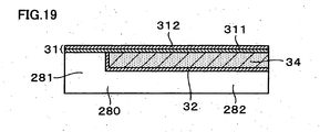
- a support member 280 supporting the fixed end of the cantilever 22 has an approximately L-shaped cross-section. That is, as shown in Fig. 16, the support member 280 has a base portion 281 bonded to the fixed end 221 and an extending portion 282 extending from the base portion 281 to the side of the free end 222 of the cantilever 22, and a space 289 is provided between the cantilever 22 and the extending portion 282.
- the magnet body 21a (21b) is disposed on a surface of the free end 222 of the cantilever 22 which is opposite to the space 289 side.
- the magnet body 21a (21b) may be formed to have a length L of 0.2 to 0.6 mm, a width W of 0.2 to 0.8 mm, and a height H of 0.05 to 0.2 mm.
- the length L is a length from the fixed end 221 of the cantilever 22 to the free end 222.
- the width W is a width orthogonal to the direction of the length L and parallel to the surface of the cantilever 22.
- the height H is a height orthogonal to the surface of the cantilever 22.
- the cantilever 22 is made of a Ni-P alloy and the support member 280 is made of a ceramic.
- a multiple metal-layer 31 composed of a plurality of metal layers is provided between the support member 280 and the fixed end 221 of the cantilever 22.
- the multiple metal-layer 31 is composed of a first metal layer 311 provided adjacent to the support member 280 and a second metal layer 312 provided adjacent to the cantilever 22.
- the first metal layer 311 is composed of at least one element of Ti, Cr, and Al
- the second metal layer 312 is composed of at least one of Cu, Au, and Ag.
- the support member 280 has a conductive layer 32 on a surface of the extending portion 282 facing the cantilever 22, and this conductive layer 32 is electrically connected to the cantilever 22.
- the conductive layer 32 is preferably connected to the ground of the electrical circuit formed on the IC substrate 10.
- the conductive layer 32 is preferably formed on the entire facing surface but may be formed on a part thereof.
- the magnet body 21a (21b) includes a resin magnet or includes a magnet and a resin layer which is to be bonded to the cantilever 22.
- the cantilever 22 is provided with a metal layer (passivation film-forming metal layer 33) forming a stable passive film which is to be bonded to the magnet body 21a (21b).
- This passivation film-forming metal layer 33 is formed using one of Cr, Al, Zn, and Ti.
- the magnet body 21a (21b) has a resin layer which is to be bonded to the cantilever 22 as described above.
- the magnet body 21a (21b) is a resin magnet
- the magnet body 21a (21b) is directly formed on the passivation film-forming metal layer 33 provided on the cantilever 22.
- the acceleration sensing part 20 being formed in combination of the cantilever 22 and the support member 280.
- the L-shaped support member 280 made of a ceramic is formed.
- the support member 280 has a width w of 0.6 mm, a length a1 of 2.0 mm, a height h1 of the base portion 281 of 0.4 mm, a height h2 of the extending portion 282 of 0.3 mm, and a length a2 of the base portion 281 of 0.4 mm.
- the conductive layer 32 is formed by sputtering Cr to have a thickness of 0.1 ⁇ m.
- a sacrifice layer 34 is formed on the conductive layer 32 provided on the L-shaped step portion 288 to form a rectangular parallelepiped on the whole, the sacrifice layer 34 being a layer to be removed in a subsequent step.
- a Ti layer having a thickness of 0.07 ⁇ m is formed by sputtering, and in addition, in a vacuum state, a Cu layer having a thickness of 0.3 ⁇ m is also formed by sputtering, thereby forming the multiple metal-layer 31 composed of the first metal layer 311 and the second metal layer 312.
- the cantilever 22 is formed using a Ni-P alloy by pattern plating.
- the cantilever 22 has a thickness of 3 ⁇ m, a width of 0.5 mm, and a length of 1.9 mm.
- a passive film-forming metal layer 33 is formed by sputtering Cr in an area in which the magnet body 21a (21b) is to be disposed.
- sputtering Cr instead of the sputtering described above, another known film forming means such as PVD or CVD may be used.
- an ink magnet material 219 composed of SmFeN (75 percent by weight) and an epoxy resin (25 percent by weight) is printed.
- the orientation described above is a step required when the ink magnetic material 219 is an anisotropic material, and when an isotropic material is used, the step described above is not necessary.
- the sacrifice layer 34, the Ti layer, and the Cu layer are removed, the latter two layers being provided on the sacrifice layer 34, so that the cantilever 22 is formed of a Ni-P single layer. Furthermore, by heating the acceleration sensing part 20 to 100°C or more, the magnet body 21a (21b) is processed by heat treatment. Next, the acceleration sensing part 20 thus obtained is fixed on a predetermined position of the IC substrate 10 as shown in Fig. 15.
- the magnet body 21a (21b) may be formed by a known method, and as described above, for example, the ink magnet material is preferably used.
- the manufacturing methods for example, a printing, dispensing, adhering, dipping, and vapor deposition (PVD, CVD) method may be mentioned.
- a sintered magnet, a bonded magnet, and the like may also be used.
- a magnet material a metal magnet such as a ferrite or alnico magnet, or a known magnet such as a SmCo, SmFeN, or NdFeB-based magnet may be used.
- a bonded magnet as a resin, for example, a thermosetting resin, such as an epoxy resin or a phenol resin, or a thermoplastic resin such as a polyamide resin may be used.
- a thermosetting resin such as an epoxy resin or a phenol resin
- a thermoplastic resin such as a polyamide resin
- a magnet having anisotropic properties when used as a magnet body, compared to a magnet having isotropic properties, a high signal magnetic field can be obtained.
- a method may be used in which an orientation magnetic field is applied to a printed mixture of a resin and a powdered magnet, followed by magnetization.
- the coercive force of a magnet body for example, since a soldering temperature of 180 to 300°C is used in mounting the acceleration sensing part 20 on the IC substrate 10, a coercive force of 0.64 MA/m or more is required.
- the magnet body to be used is not limited to that described above.
- the rest of the structure of the accelerometer 1 of this embodiment other than the acceleration sensing part 20 described above is the same as that in Embodiment 1.
- the support member 280 has the base portion 281 and the extending portion 282, when the support member 280 (acceleration sensing part 20) fixing the cantilever 22 is mounted on the IC substrate 10, the acceleration sensing part 20 can be easily handled.
- the support member 280 when the acceleration sensing part 20 is handled, in order to prevent the cantilever 22 from being deformed, a portion other than the cantilever 22, that is, the support member 280 is preferably held.
- the support member 280 when the support member 280 is formed to have the shape as described above, the support member 280 can be easily held, and hence the acceleration sensing part 20 can be easily handled.
- the length a1 of the support member 280 is formed slightly larger (such as approximately 0.1 mm) than that of the cantilever 22, the support member 280 can be easily held at the two ends thereof in the longitudinal direction without touching the cantilever 22.
- the cantilever 22 is made of a Ni-P alloy, a cantilever can be formed having superior spring properties, such as a low elastic modulus, a wide elastic deformation region, and a high breaking strength. Hence, the cantilever 22 can be formed so as to have a high acceleration-detecting accuracy and superior durability.
- a material for the cantilever 22 any materials having properties equivalent or superior to those described above may also be used.
- the multiple metal-layer 31 is provided between the support member 280 and the fixed end 221 of the cantilever 22, the adhesion therebetween can be improved. That is, the multiple metal-layer 31 is composed of the first metal layer 311 formed from at least one of Ti, Cr, and Al and the second metal layer 312 formed from at least one of Cu, Au, and Ag. Accordingly, since bonding to the support member 280 is secured by the first metal layer 312, and bonding to the cantilever 22 is secured by the second metal layer 312, the adhesion between the support member 280 and the cantilever 22 can be further improved.
- the accelerometer 1 can be formed to have a higher accuracy.
- the cantilever 22 is provided with the passive film-forming metal layer 33 on the surface thereof in an area to be bonded to the magnet body 21a (21b). Since the affinity between the passivation film and the resin is high, the adhesion between the cantilever 22 and the magnet body 21a (21b) can be improved. That is, since the passivation film has reactive functional groups such as an oxygen-containing group and a hydroxyl group on the surface thereof, high affinity of the passivation film to a resin can be obtained. In addition, in a stable passivation film, the reactive functional groups such as an oxygen-containing group and a hydroxyl group are uniformly present on the surface thereof, and hence the affinity to a resin can be further increased. As described above, by increasing a chemical bonding force between the Ni-P alloy and the resin, the bonding between the cantilever 22 and the magnet body 21a (21b) can be improved.
- the passive film-forming metal layer 33 described above is formed from one of Cr, Al, Zn, and Ti, a particularly stable passive film can be formed.
- the operational effects equivalent to that of Embodiment 1 are also obtained. This embodiment may also be applied to various structures shown in Embodiment 2.
- a reinforcing layer 223 is provided on the magnet fixing region of the cantilever 22.
- the magnet body 21 is disposed on the reinforcing layer 223 with the passive film-forming metal layer 33 interposed therebetween.
- a reinforcing layer 224 is also formed on the fixed end 221 of the cantilever 22.
- the reinforcing layers 223 and 224 each have a thickness, for example, of 3 to 100 ⁇ m.
- the manufacturing method of the acceleration sensing part 20 of the accelerometer 1 of this embodiment is basically equivalent to that described in Embodiment 3.
- Ni-P layers having a thickness of 20 ⁇ m are formed by plating. Accordingly, the reinforcing layers 223 and 224 are formed.
- the rest of the structure is the same as that in Embodiment 3, and the same operational effects as that thereof are also obtained.
- Figs. 25 and 26 the case in which an opening 225 is provided in the cantilever 22 will be described.
- the opening 225 is formed between the fixed end 221 and the magnet body 21.
- Fig. 25 shows the case in which the opening 225 is provided in the acceleration sensing part 20 of Embodiment 3
- Fig. 26 shows the case in which the opening 225 is provided in the acceleration sensing part 20 of Embodiment 4.
- the opening 225 is provided in a region in which the reinforcing layers 223 and 224 are not formed.
- the rest of the structure is the same as that in Embodiment 3 or 4.
- the elastic modulus of the cantilever 22 can be partly decreased, and hence the amount of elastic deformation of the cantilever 22 with respect to a predetermined acceleration can be increased. Accordingly, the accelerometer 1 can be formed to have higher sensitivity. In addition, the operational effects equivalent to that of Embodiment 3 or 4 are also obtained.
- stoppers 51 and 52 are provided at the two sides of the rotational direction of the free end 222 of the cantilever 22 for preventing excessive displacement thereof.
- One stopper 52 of the two stoppers 51 and 52 is integrally formed with the support member 280. That is, the extending portion 282 of the support member 280 functions as the stopper 52.
- the stopper 51 independent of the support member 280 is fixed on the IC substrate 10. Also in this embodiment, the acceleration sensing part 20 (see Fig. 16) shown in Embodiment 3 is used.
- the stopper 51 is disposed at the side of the free end 22 of the cantilever 22 of the acceleration sensing part 20.
- a space d1 between this stopper 51 and the'extending portion 282 (stopper 52) of the acceleration sensing part 20 may be formed, for example, to have 0.4 mm.
- a space d2 between the stopper 51 and the magnet body 21a (21b) disposed at the free end 222 of the cantilever 22 may be formed, for example, to have 0.18 mm
- a space d3 between the stopper 52 (extending portion 282) and the free end 222 of the cantilever 22 may be formed, for example, to have 0.08 mm.
- a length w3 of the stopper 51 in an erection direction with respect to the IC substrate 10 is preferably approximately equivalent to that of the support member 280 in the erection direction therewith, and for example, the length w3 may be set to 0.55 mm.
- a length h3 in a direction orthogonal to the cantilever 22 and a length a3 in a direction parallel thereto may be set to 0.5 mm and 0.9 mm, respectively.
- the stopper 51 and the support member 280 are formed of silicon (Si).
- a peripheral magnetic field detecting portion 43c detecting a Z axis direction component of a peripheral magnetic field is provided.
- the rest of the structure is the same as that in Embodiment 3.
- the stopper 52 is integrally formed with the support member 280, the number of parts forming the accelerometer 1 can be decreased, and as a result, easy assembly and reduction in cost can be advantageously obtained. Furthermore, the same operational effects as those of Embodiment 3 are also obtained.
- the terms to "rotate” or “rotating” or “rotation” or the like used in the description and in the claims with respect to the cantilever movement and the like comprise the meaning of to "pivot” or “pivoting” such as around a fulcrum axis. In other words, the meaning of "rotating” includes the meaning of "pivoting" around the fixed end of the cantilever as an imaginary fulcrum axis.
Landscapes
- Physics & Mathematics (AREA)
- General Physics & Mathematics (AREA)
- Measuring Magnetic Variables (AREA)
- Micromachines (AREA)
- Measurement Of Length, Angles, Or The Like Using Electric Or Magnetic Means (AREA)
- Pressure Sensors (AREA)
Applications Claiming Priority (6)
| Application Number | Priority Date | Filing Date | Title |
|---|---|---|---|
| JP2004135082 | 2004-04-30 | ||
| JP2004135082 | 2004-04-30 | ||
| JP2004283700 | 2004-09-29 | ||
| JP2004283700 | 2004-09-29 | ||
| JP2004356999 | 2004-12-09 | ||
| JP2004356999 | 2004-12-09 |
Publications (2)
| Publication Number | Publication Date |
|---|---|
| EP1591792A2 true EP1591792A2 (de) | 2005-11-02 |
| EP1591792A3 EP1591792A3 (de) | 2006-05-24 |
Family
ID=34935730
Family Applications (1)
| Application Number | Title | Priority Date | Filing Date |
|---|---|---|---|
| EP05009085A Withdrawn EP1591792A3 (de) | 2004-04-30 | 2005-04-26 | Beschleunigungssensor mit Kompensation für externe Magnetfelder |
Country Status (7)
| Country | Link |
|---|---|
| US (1) | US7219549B2 (de) |
| EP (1) | EP1591792A3 (de) |
| JP (1) | JP4896712B2 (de) |
| KR (2) | KR100632458B1 (de) |
| CN (2) | CN100443900C (de) |
| TW (1) | TWI263785B (de) |
| WO (1) | WO2005106502A1 (de) |
Cited By (6)
| Publication number | Priority date | Publication date | Assignee | Title |
|---|---|---|---|---|
| GB2425608A (en) * | 2005-04-28 | 2006-11-01 | Smart Stabilizer Systems Ltd | Tri-Axial Accelerometer |
| EP1770361A3 (de) * | 2005-09-29 | 2008-04-16 | Aichi Steel Corporation | Bewegungsmesser und tragbares Telefon damit |
| EP1790986A3 (de) * | 2005-11-24 | 2010-01-06 | TDK Corporation | Federelement für Beschleunigungsmesser, Beschleunigungsmesser und magnetisches Plattenlaufwerkgerät |
| US9109271B2 (en) | 2013-03-14 | 2015-08-18 | Brunswick Corporation | Nickel containing hypereutectic aluminum-silicon sand cast alloy |
| US9650699B1 (en) | 2013-03-14 | 2017-05-16 | Brunswick Corporation | Nickel containing hypereutectic aluminum-silicon sand cast alloys |
| US10370742B2 (en) | 2013-03-14 | 2019-08-06 | Brunswick Corporation | Hypereutectic aluminum-silicon cast alloys having unique microstructure |
Families Citing this family (32)
| Publication number | Priority date | Publication date | Assignee | Title |
|---|---|---|---|---|
| EP1628114B1 (de) * | 2004-05-17 | 2008-04-23 | Aichi Steel Corporation | Kleiner lagedetektor und zellulares telefon mit dem detektor |
| JP2007033045A (ja) * | 2005-07-22 | 2007-02-08 | Tdk Corp | 加速度センサ用のばね部材、加速度センサ及び磁気ディスクドライブ装置 |
| US20070209437A1 (en) * | 2005-10-18 | 2007-09-13 | Seagate Technology Llc | Magnetic MEMS device |
| JP2007147304A (ja) * | 2005-11-24 | 2007-06-14 | Tdk Corp | 加速度センサ及び磁気ディスクドライブ装置 |
| JP4222375B2 (ja) * | 2006-02-09 | 2009-02-12 | Tdk株式会社 | 加速度センサ及び磁気ディスクドライブ装置 |
| JP4285488B2 (ja) * | 2006-02-16 | 2009-06-24 | Tdk株式会社 | 加速度センサ及び磁気ディスクドライブ装置 |
| DE102006010484A1 (de) * | 2006-03-07 | 2007-09-13 | Robert Bosch Gmbh | Bewegungssensor |
| US20070251320A1 (en) * | 2006-04-28 | 2007-11-01 | Russell Michael K | Tri-axial accelerometer |
| WO2008016198A1 (en) * | 2006-08-03 | 2008-02-07 | Microgate, Inc. | 3 axis thin film fluxgate |
| US7541939B2 (en) * | 2007-03-15 | 2009-06-02 | Apple Inc. | Mounted shock sensor |
| KR101132263B1 (ko) * | 2010-01-08 | 2012-04-02 | 주식회사 이노칩테크놀로지 | 가속도 센싱 조립체와 그 제작 방법 |
| DE102012009570A1 (de) * | 2012-05-09 | 2013-11-14 | Naum Goldstein | Komposition für nasale Anwendung |
| US10108265B2 (en) * | 2012-05-09 | 2018-10-23 | Apple Inc. | Calibration of haptic feedback systems for input devices |
| AU2013260186A1 (en) | 2012-05-09 | 2014-12-04 | Apple Inc. | Thresholds for determining feedback in computing devices |
| US20150109223A1 (en) | 2012-06-12 | 2015-04-23 | Apple Inc. | Haptic electromagnetic actuator |
| US9886116B2 (en) | 2012-07-26 | 2018-02-06 | Apple Inc. | Gesture and touch input detection through force sensing |
| US20140290365A1 (en) * | 2013-04-02 | 2014-10-02 | Tao Ju | Mems device |
| CN103076577B (zh) * | 2012-08-03 | 2016-12-21 | 陈磊 | 一种检测磁场和加速度的磁阻传感器芯片 |
| US9297824B2 (en) | 2012-09-14 | 2016-03-29 | Intel Corporation | Techniques, systems and devices related to acceleration measurement |
| US9250261B2 (en) * | 2012-12-28 | 2016-02-02 | Intel Corporation | Method, apparatus and system for providing metering of acceleration |
| US20150242037A1 (en) | 2014-01-13 | 2015-08-27 | Apple Inc. | Transparent force sensor with strain relief |
| US9839783B2 (en) | 2014-07-25 | 2017-12-12 | Medtronic, Inc. | Magnetic field detectors, implantable medical devices, and related methods that utilize a suspended proof mass and magnetically sensitive material |
| US10297119B1 (en) | 2014-09-02 | 2019-05-21 | Apple Inc. | Feedback device in an electronic device |
| US9939901B2 (en) | 2014-09-30 | 2018-04-10 | Apple Inc. | Haptic feedback assembly |
| US9798409B1 (en) | 2015-03-04 | 2017-10-24 | Apple Inc. | Multi-force input device |
| EP3147258A1 (de) * | 2015-09-22 | 2017-03-29 | AT & S Austria Technologie & Systemtechnik Aktiengesellschaft | Verbindungspaneel für elektronische bauelemente |
| CN106940386A (zh) * | 2017-03-03 | 2017-07-11 | 北京航空航天大学 | 一种传感模块及加速度计 |
| CN109991444A (zh) * | 2017-12-30 | 2019-07-09 | 大连良华科技有限公司 | 一种应变式加速度传感器 |
| JP2021089273A (ja) * | 2019-11-26 | 2021-06-10 | ローム株式会社 | 磁界検出装置 |
| CN113029204B (zh) * | 2021-03-01 | 2023-06-23 | 歌尔微电子股份有限公司 | 传感器和电子设备 |
| CN114705417B (zh) * | 2022-03-29 | 2026-03-06 | 江苏科技大学 | 一种用于海上风电齿轮箱剩余寿命预测的试验装置及方法 |
| CN116754792A (zh) * | 2023-05-24 | 2023-09-15 | 宁波萨瑞通讯有限公司 | 加速度方向判断电路及方法 |
Citations (11)
| Publication number | Priority date | Publication date | Assignee | Title |
|---|---|---|---|---|
| US4212041A (en) | 1977-04-29 | 1980-07-08 | Compagnie Internationale Pour L'informatique | Apparatus and method for removing the effect of interference magnetic fields in a magnetic transducer device for detecting information magnetically coded on a carrier |
| US4603665A (en) | 1985-04-15 | 1986-08-05 | Brunswick Corp. | Hypereutectic aluminum-silicon casting alloy |
| EP0251069A1 (de) | 1986-06-20 | 1988-01-07 | Atsugi Unisia Corporation | Beschleunigungsmesser |
| US4849655A (en) | 1985-07-04 | 1989-07-18 | Hayman-Reese Party, Limited | Accelerometer or decelerometer for vehicle brake control system |
| WO1989010570A1 (en) | 1988-04-21 | 1989-11-02 | Omega Electric Limited | Magnetic field detection system |
| EP0431807A1 (de) | 1989-11-29 | 1991-06-12 | Honeywell Inc. | Ein durch in sich geschlossenes viskoses Material gedämpfter Beschleunigungsmesser |
| US5027657A (en) | 1988-12-09 | 1991-07-02 | Alfred Teves Gmbh | Acceleration sensor with cantilevered bending beam |
| US5694041A (en) | 1994-07-05 | 1997-12-02 | Sextant Avionique | Method of compensation of electromagnetic perturbations due to moving magnetic and conducting objects |
| JP2000258449A (ja) | 1999-03-05 | 2000-09-22 | Canon Electronics Inc | 磁気式加速度センサ及び加速度検知装置 |
| JP2003315431A (ja) | 2002-04-23 | 2003-11-06 | Toyoda Mach Works Ltd | 透磁率センサ、距離センサ、受圧力センサ |
| JP2004119517A (ja) | 2002-09-24 | 2004-04-15 | Ricoh Co Ltd | Miセンサ、miセンサ用のicチップおよびそのmiセンサを備えた電子装置 |
Family Cites Families (10)
| Publication number | Priority date | Publication date | Assignee | Title |
|---|---|---|---|---|
| JPS58154615A (ja) | 1982-03-10 | 1983-09-14 | Copal Co Ltd | 磁気検出装置 |
| DE3704209A1 (de) * | 1986-04-11 | 1987-10-15 | Bosch Gmbh Robert | Beschleunigungssensor |
| JPH077012B2 (ja) * | 1987-08-18 | 1995-01-30 | 富士通株式会社 | 加速度センサ |
| US5627315A (en) * | 1995-04-18 | 1997-05-06 | Honeywell Inc. | Accelerometer with a cantilever beam formed as part of the housing structure |
| JPH09222367A (ja) * | 1996-02-15 | 1997-08-26 | Sony Corp | 力検出センサ |
| JP2000055930A (ja) * | 1998-06-03 | 2000-02-25 | Yaskawa Electric Corp | 加速度センサ |
| US6311557B1 (en) * | 1999-09-24 | 2001-11-06 | Ut-Battelle, Llc | Magnetically tunable resonance frequency beam utilizing a stress-sensitive film |
| US6698295B1 (en) | 2000-03-31 | 2004-03-02 | Shipley Company, L.L.C. | Microstructures comprising silicon nitride layer and thin conductive polysilicon layer |
| JP4491114B2 (ja) * | 2000-06-23 | 2010-06-30 | 株式会社日立グローバルストレージテクノロジーズ | 落下感知センサ及びこれを用いた情報処理装置 |
| JP2002040043A (ja) * | 2000-07-19 | 2002-02-06 | Yaskawa Electric Corp | 加速度センサ |
-
2005
- 2005-03-17 KR KR1020050022336A patent/KR100632458B1/ko not_active Expired - Fee Related
- 2005-03-21 US US11/084,818 patent/US7219549B2/en not_active Expired - Fee Related
- 2005-04-04 TW TW094110771A patent/TWI263785B/zh not_active IP Right Cessation
- 2005-04-21 CN CNB2005100670305A patent/CN100443900C/zh not_active Expired - Fee Related
- 2005-04-26 EP EP05009085A patent/EP1591792A3/de not_active Withdrawn
- 2005-04-28 KR KR1020067017529A patent/KR100810591B1/ko not_active Expired - Fee Related
- 2005-04-28 CN CN2005800094281A patent/CN1938593B/zh not_active Expired - Fee Related
- 2005-04-28 WO PCT/JP2005/008136 patent/WO2005106502A1/ja not_active Ceased
- 2005-04-28 JP JP2006512833A patent/JP4896712B2/ja not_active Expired - Fee Related
Patent Citations (12)
| Publication number | Priority date | Publication date | Assignee | Title |
|---|---|---|---|---|
| US4212041A (en) | 1977-04-29 | 1980-07-08 | Compagnie Internationale Pour L'informatique | Apparatus and method for removing the effect of interference magnetic fields in a magnetic transducer device for detecting information magnetically coded on a carrier |
| US4603665A (en) | 1985-04-15 | 1986-08-05 | Brunswick Corp. | Hypereutectic aluminum-silicon casting alloy |
| US4849655A (en) | 1985-07-04 | 1989-07-18 | Hayman-Reese Party, Limited | Accelerometer or decelerometer for vehicle brake control system |
| EP0251069A1 (de) | 1986-06-20 | 1988-01-07 | Atsugi Unisia Corporation | Beschleunigungsmesser |
| WO1989010570A1 (en) | 1988-04-21 | 1989-11-02 | Omega Electric Limited | Magnetic field detection system |
| US5027657A (en) | 1988-12-09 | 1991-07-02 | Alfred Teves Gmbh | Acceleration sensor with cantilevered bending beam |
| EP0431807A1 (de) | 1989-11-29 | 1991-06-12 | Honeywell Inc. | Ein durch in sich geschlossenes viskoses Material gedämpfter Beschleunigungsmesser |
| US5694041A (en) | 1994-07-05 | 1997-12-02 | Sextant Avionique | Method of compensation of electromagnetic perturbations due to moving magnetic and conducting objects |
| JP2000258449A (ja) | 1999-03-05 | 2000-09-22 | Canon Electronics Inc | 磁気式加速度センサ及び加速度検知装置 |
| JP2003315431A (ja) | 2002-04-23 | 2003-11-06 | Toyoda Mach Works Ltd | 透磁率センサ、距離センサ、受圧力センサ |
| JP2004119517A (ja) | 2002-09-24 | 2004-04-15 | Ricoh Co Ltd | Miセンサ、miセンサ用のicチップおよびそのmiセンサを備えた電子装置 |
| US20040124835A1 (en) | 2002-09-24 | 2004-07-01 | Takeshi Kimura | Miniaturized magnetic impedance sensor with an IC chip having an electrode near a magnetic impedance element |
Cited By (8)
| Publication number | Priority date | Publication date | Assignee | Title |
|---|---|---|---|---|
| GB2425608A (en) * | 2005-04-28 | 2006-11-01 | Smart Stabilizer Systems Ltd | Tri-Axial Accelerometer |
| GB2425608B (en) * | 2005-04-28 | 2009-02-18 | Smart Stabilizer Systems Ltd | Tri-axial accelerometer |
| EP1770361A3 (de) * | 2005-09-29 | 2008-04-16 | Aichi Steel Corporation | Bewegungsmesser und tragbares Telefon damit |
| US7886600B2 (en) | 2005-09-29 | 2011-02-15 | Aichi Steel Corporation | Motion sensor and portable telephone using the same |
| EP1790986A3 (de) * | 2005-11-24 | 2010-01-06 | TDK Corporation | Federelement für Beschleunigungsmesser, Beschleunigungsmesser und magnetisches Plattenlaufwerkgerät |
| US9109271B2 (en) | 2013-03-14 | 2015-08-18 | Brunswick Corporation | Nickel containing hypereutectic aluminum-silicon sand cast alloy |
| US9650699B1 (en) | 2013-03-14 | 2017-05-16 | Brunswick Corporation | Nickel containing hypereutectic aluminum-silicon sand cast alloys |
| US10370742B2 (en) | 2013-03-14 | 2019-08-06 | Brunswick Corporation | Hypereutectic aluminum-silicon cast alloys having unique microstructure |
Also Published As
| Publication number | Publication date |
|---|---|
| JP4896712B2 (ja) | 2012-03-14 |
| KR100632458B1 (ko) | 2006-10-11 |
| CN1938593B (zh) | 2010-12-29 |
| US20060123906A1 (en) | 2006-06-15 |
| KR20070005607A (ko) | 2007-01-10 |
| KR100810591B1 (ko) | 2008-03-07 |
| JPWO2005106502A1 (ja) | 2008-03-21 |
| WO2005106502A1 (ja) | 2005-11-10 |
| KR20060043771A (ko) | 2006-05-15 |
| US7219549B2 (en) | 2007-05-22 |
| TW200537098A (en) | 2005-11-16 |
| CN1938593A (zh) | 2007-03-28 |
| TWI263785B (en) | 2006-10-11 |
| CN1693900A (zh) | 2005-11-09 |
| EP1591792A3 (de) | 2006-05-24 |
| CN100443900C (zh) | 2008-12-17 |
Similar Documents
| Publication | Publication Date | Title |
|---|---|---|
| US7219549B2 (en) | Accelerometer with cantilever and magnetic field detector | |
| EP2413153B9 (de) | Magnetdetektionsvorrichtung | |
| US7453269B2 (en) | Magnetic MEMS sensor device | |
| JP2009122041A (ja) | 複合センサー | |
| US7886600B2 (en) | Motion sensor and portable telephone using the same | |
| JPH11352143A (ja) | 加速度センサ | |
| US20110316531A1 (en) | Device for measuring the direction and/or strength of a magnetic field | |
| EP2339362A1 (de) | Magnetsensormodul und Bolzenpositionsdetektor | |
| KR20070060109A (ko) | 센서 장치 및 디바이스 | |
| JP2010091565A (ja) | 微小電気機械システム(mems)力平行加速度計 | |
| US7420364B2 (en) | Small-sized attitude detection sensor and portable telephone using the small-sized attitude detection sensor | |
| JP2009511907A (ja) | 微小電子機械磁力計 | |
| WO2005103727A1 (ja) | 加速度センサ | |
| JP5240657B2 (ja) | センシング素子、センシング装置、方位検出装置及び情報機器 | |
| JP4230249B2 (ja) | スロットル開度検知装置 | |
| CN106771354A (zh) | 一种单轴mems加速度计 | |
| RU2506546C1 (ru) | Микроэлектромеханический датчик микроперемещений с магнитным полем | |
| JPH04184171A (ja) | 加速度センサ | |
| JP2004233212A (ja) | 加速度センサ及び加速度検出装置 |
Legal Events
| Date | Code | Title | Description |
|---|---|---|---|
| PUAI | Public reference made under article 153(3) epc to a published international application that has entered the european phase |
Free format text: ORIGINAL CODE: 0009012 |
|
| 17P | Request for examination filed |
Effective date: 20050426 |
|
| AK | Designated contracting states |
Kind code of ref document: A2 Designated state(s): AT BE BG CH CY CZ DE DK EE ES FI FR GB GR HU IE IS IT LI LT LU MC NL PL PT RO SE SI SK TR |
|
| AX | Request for extension of the european patent |
Extension state: AL BA HR LV MK YU |
|
| PUAL | Search report despatched |
Free format text: ORIGINAL CODE: 0009013 |
|
| AK | Designated contracting states |
Kind code of ref document: A3 Designated state(s): AT BE BG CH CY CZ DE DK EE ES FI FR GB GR HU IE IS IT LI LT LU MC NL PL PT RO SE SI SK TR |
|
| AX | Request for extension of the european patent |
Extension state: AL BA HR LV MK YU |
|
| AKX | Designation fees paid |
Designated state(s): DE FR GB |
|
| 17Q | First examination report despatched |
Effective date: 20100406 |
|
| STAA | Information on the status of an ep patent application or granted ep patent |
Free format text: STATUS: THE APPLICATION IS DEEMED TO BE WITHDRAWN |
|
| 18D | Application deemed to be withdrawn |
Effective date: 20121101 |