EP1589413A2 - Cryptographic processor - Google Patents
Cryptographic processor Download PDFInfo
- Publication number
- EP1589413A2 EP1589413A2 EP05012165A EP05012165A EP1589413A2 EP 1589413 A2 EP1589413 A2 EP 1589413A2 EP 05012165 A EP05012165 A EP 05012165A EP 05012165 A EP05012165 A EP 05012165A EP 1589413 A2 EP1589413 A2 EP 1589413A2
- Authority
- EP
- European Patent Office
- Prior art keywords
- sub
- partial
- operations
- control unit
- calculators
- Prior art date
- Legal status (The legal status is an assumption and is not a legal conclusion. Google has not performed a legal analysis and makes no representation as to the accuracy of the status listed.)
- Granted
Links
Images

Classifications
-
- H—ELECTRICITY
- H04—ELECTRIC COMMUNICATION TECHNIQUE
- H04L—TRANSMISSION OF DIGITAL INFORMATION, e.g. TELEGRAPHIC COMMUNICATION
- H04L9/00—Cryptographic mechanisms or cryptographic arrangements for secret or secure communications; Network security protocols
-
- G—PHYSICS
- G06—COMPUTING OR CALCULATING; COUNTING
- G06F—ELECTRIC DIGITAL DATA PROCESSING
- G06F9/00—Arrangements for program control, e.g. control units
- G06F9/06—Arrangements for program control, e.g. control units using stored programs, i.e. using an internal store of processing equipment to receive or retain programs
- G06F9/30—Arrangements for executing machine instructions, e.g. instruction decode
- G06F9/38—Concurrent instruction execution, e.g. pipeline or look ahead
- G06F9/3885—Concurrent instruction execution, e.g. pipeline or look ahead using a plurality of independent parallel functional units
- G06F9/3889—Concurrent instruction execution, e.g. pipeline or look ahead using a plurality of independent parallel functional units controlled by multiple instructions, e.g. MIMD, decoupled access or execute
- G06F9/3891—Concurrent instruction execution, e.g. pipeline or look ahead using a plurality of independent parallel functional units controlled by multiple instructions, e.g. MIMD, decoupled access or execute organised in groups of units sharing resources, e.g. clusters
-
- G—PHYSICS
- G06—COMPUTING OR CALCULATING; COUNTING
- G06F—ELECTRIC DIGITAL DATA PROCESSING
- G06F21/00—Security arrangements for protecting computers, components thereof, programs or data against unauthorised activity
- G06F21/70—Protecting specific internal or peripheral components, in which the protection of a component leads to protection of the entire computer
- G06F21/71—Protecting specific internal or peripheral components, in which the protection of a component leads to protection of the entire computer to assure secure computing or processing of information
- G06F21/72—Protecting specific internal or peripheral components, in which the protection of a component leads to protection of the entire computer to assure secure computing or processing of information in cryptographic circuits
-
- G—PHYSICS
- G06—COMPUTING OR CALCULATING; COUNTING
- G06F—ELECTRIC DIGITAL DATA PROCESSING
- G06F21/00—Security arrangements for protecting computers, components thereof, programs or data against unauthorised activity
- G06F21/70—Protecting specific internal or peripheral components, in which the protection of a component leads to protection of the entire computer
- G06F21/71—Protecting specific internal or peripheral components, in which the protection of a component leads to protection of the entire computer to assure secure computing or processing of information
- G06F21/75—Protecting specific internal or peripheral components, in which the protection of a component leads to protection of the entire computer to assure secure computing or processing of information by inhibiting the analysis of circuitry or operation
- G06F21/755—Protecting specific internal or peripheral components, in which the protection of a component leads to protection of the entire computer to assure secure computing or processing of information by inhibiting the analysis of circuitry or operation with measures against power attack
-
- G—PHYSICS
- G06—COMPUTING OR CALCULATING; COUNTING
- G06F—ELECTRIC DIGITAL DATA PROCESSING
- G06F7/00—Methods or arrangements for processing data by operating upon the order or content of the data handled
- G06F7/60—Methods or arrangements for performing computations using a digital non-denominational number representation, i.e. number representation without radix; Computing devices using combinations of denominational and non-denominational quantity representations, e.g. using difunction pulse trains, STEELE computers, phase computers
- G06F7/72—Methods or arrangements for performing computations using a digital non-denominational number representation, i.e. number representation without radix; Computing devices using combinations of denominational and non-denominational quantity representations, e.g. using difunction pulse trains, STEELE computers, phase computers using residue arithmetic
-
- G—PHYSICS
- G06—COMPUTING OR CALCULATING; COUNTING
- G06F—ELECTRIC DIGITAL DATA PROCESSING
- G06F9/00—Arrangements for program control, e.g. control units
- G06F9/06—Arrangements for program control, e.g. control units using stored programs, i.e. using an internal store of processing equipment to receive or retain programs
- G06F9/30—Arrangements for executing machine instructions, e.g. instruction decode
- G06F9/38—Concurrent instruction execution, e.g. pipeline or look ahead
- G06F9/3877—Concurrent instruction execution, e.g. pipeline or look ahead using a secondary processor, e.g. coprocessor
- G06F9/3879—Concurrent instruction execution, e.g. pipeline or look ahead using a secondary processor, e.g. coprocessor for non-native instruction execution, e.g. executing a command; for Java instruction set
-
- G—PHYSICS
- G06—COMPUTING OR CALCULATING; COUNTING
- G06F—ELECTRIC DIGITAL DATA PROCESSING
- G06F9/00—Arrangements for program control, e.g. control units
- G06F9/06—Arrangements for program control, e.g. control units using stored programs, i.e. using an internal store of processing equipment to receive or retain programs
- G06F9/30—Arrangements for executing machine instructions, e.g. instruction decode
- G06F9/38—Concurrent instruction execution, e.g. pipeline or look ahead
- G06F9/3885—Concurrent instruction execution, e.g. pipeline or look ahead using a plurality of independent parallel functional units
-
- G—PHYSICS
- G06—COMPUTING OR CALCULATING; COUNTING
- G06F—ELECTRIC DIGITAL DATA PROCESSING
- G06F2207/00—Indexing scheme relating to methods or arrangements for processing data by operating upon the order or content of the data handled
- G06F2207/72—Indexing scheme relating to groups G06F7/72 - G06F7/729
- G06F2207/7219—Countermeasures against side channel or fault attacks
- G06F2207/7266—Hardware adaptation, e.g. dual rail logic; calculate add and double simultaneously
-
- G—PHYSICS
- G06—COMPUTING OR CALCULATING; COUNTING
- G06F—ELECTRIC DIGITAL DATA PROCESSING
- G06F7/00—Methods or arrangements for processing data by operating upon the order or content of the data handled
- G06F7/60—Methods or arrangements for performing computations using a digital non-denominational number representation, i.e. number representation without radix; Computing devices using combinations of denominational and non-denominational quantity representations, e.g. using difunction pulse trains, STEELE computers, phase computers
- G06F7/72—Methods or arrangements for performing computations using a digital non-denominational number representation, i.e. number representation without radix; Computing devices using combinations of denominational and non-denominational quantity representations, e.g. using difunction pulse trains, STEELE computers, phase computers using residue arithmetic
- G06F7/723—Modular exponentiation
Definitions
- the present invention relates to cryptographic techniques and in particular on the architecture of cryptographic Applications used cryptographic processors.
- cryptography techniques on the one hand include cryptographic algorithms and on the other hand, suitable processor solutions which the computations prescribed by the cryptographic algorithms To run.
- cryptographic algorithms are more and more on Smart cards or special security ICs are executed, for which special requirements apply.
- cryptographic processors have a considerable Provide computing power, especially the security many cryptographic algorithms such.
- a high computational effort also means a high computing time, so for cryptography processors at the same time also the essential requirement is a high Computer throughput, so that, for example, an identification, an access to a building, a payment transaction or a credit card transfer not many Minutes, which would be very damaging for the market acceptance.
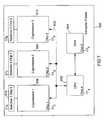
- FIG. Fig. 7 shows a Computer board 800, on which a CPU 802, a working memory (RAM) 804, a first coprocessor 806, a second coprocessor 808 and a third coprocessor 810 arranged are.
- the CPU 802 is connected to the three coprocessors 806, 808, 810 connected via a bus 812.
- a separate memory may be provided which only for coprocessor operations, i. H. a memory 1 814, a memory 2 816 for the coprocessor 2 and a memory 3 818 for the coprocessor 3.
- each chip disposed on the computer board 800 shown in FIG. 7 is supplied with the electric power required for the functioning of the electronic components within the individual elements via its own power supply terminal I 1 to I 8 .
- the board 800 is then distributed via the board to the individual chips on the board.
- the supply lines to the individual chips are available for an attacker.
- each chip on the computer board 800 has a own power or power access, on the without Another of an attacker can be accessed Tapping power profiles or power profiles over time. Capturing performance profiles over time is the foundation faced with a variety of efficient attacks Cryptographic processors. More backgrounds or a detailed Representation of various attacks against cryptography processors are in "Information Leakage Attacks A-gainst Smart Card Implementations of Cryptographic Algorithms and Countermeasures ", Hess et al., Eurosmart Security Conference, June 13 to June 15, 2000, presented. As countermeasures Implementations are proposed which are based on it build up that different operations are always the same Need time, allowing an attacker due to a performance profile can not see if the crypto processor has a Multiplication, an addition, or anything else Has.
- the ZDN method is based on a serial / parallel architecture using parallel executable look-ahead Algorithms for multiplication and modular reduction, by a multiplication of two binary numbers into one iterative 3-operand addition using look-ahead parameters for multiplication and modular reduction to transform.
- This is the modular multiplication decomposed into a serial calculation of partial products.
- two partial products are formed and then taking into account the modular reduction added together to get an intermediate result.
- another partial product is formed and again taking into account the modular reduction to the intermediate result added.
- This iteration continues until all parts of the multiplier have been processed.
- For the three-operand addition involves a crypto-coprocessor an adder, which is in a current iteration step the summation of a new partial product to the intermediate result of the preceding iteration step.
- each coprocessor of FIG. 7 could have its own ZDN unit be equipped to several modular multiplications run parallel to the for certain applications Increase throughput.
- this solution would turn on it fail that an attacker of each chip individually the Can elicit power profiles, so that although an increase in the Throughput has been achieved, but at the expense of security of the cryptography calculator.
- the object of the present invention is to provide a fast and secure cryptography processor.
- the present invention is based on the knowledge that a fast cryptography processor can only be achieved can, if a cryptographic compute operation in several Partial operations is decomposed, and these sub-operations of be executed parallel part calculations. on the other hand can be a security especially against performance monitoring attacks can only be achieved if all sub-calculators including the control unit for the sub-processors and the central processing unit on a single Chip can be arranged so that the power inputs for the individual components not for an external attacker To be available.
- the central processing facility and the coprocessor which has a single control unit as well Has a plurality of sub-calculations, on a single Integrated chip.
- this single chip only has a single supply access to supply the A plurality of sub-processors, the control unit and the central processing unit with power on.
- a limit of parallel processing is then reached if the computational effort in the control unit to distribute the Sub-operations on the sub-processors and for driving the individual part of the calculation increases sharply.
- the multiplication of two very long integers is the ratio of computation time in a partial calculation to the computing time of the control unit so great for organizational and administrative tasks that a considerable degree of parallelism can be achieved without the administrative burden in problematic scales comes.
- Cryptoprocessors are used for safety-critical applications used, for example, for digital signatures, authentications or encryption tasks. An attacker wants For example, find out the secret key to thereby to break the cryptography process.
- Cryptographic processors are used for example in chip cards, which, as has already been stated, smart cards or Signature cards for a legally binding electronic Signature or for home banking or to pay with the mobile phone, etc.
- Typical physical attacks measure power consumption (SPA, DPA, timing attacks) or the electromagnetic radiation.
- SPA power consumption
- DPA timing attacks
- electromagnetic radiation For a more detailed explanation of the attacks reference is made to the references mentioned above.
- an attack typically measures the power consumption of the entire chip card, including the CPU and coprocessor, which is the sum of the individual power consumptions of, for example, the CPU, the RAM, a ROM, an E 2 PROM, a flash memory, a timing controller, a random number generator (RNG), a DES module, and the crypto-coprocessor.
- the CPU and coprocessor which is the sum of the individual power consumptions of, for example, the CPU, the RAM, a ROM, an E 2 PROM, a flash memory, a timing controller, a random number generator (RNG), a DES module, and the crypto-coprocessor.
- the power consumption of an example in CMOS technology manufactured chips changes when switching from one "0" to a "1". Therefore, the power consumption is data dependent as well as the used commands of the CPU and the Cryptocoprocessor.
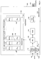
- Fig. 1 shows a cryptoprocessor according to the invention for Performing operations for cryptographic applications.
- the crypto processor is implemented on a single chip 100 and includes a central processing unit (CPU) 102 and a coprocessor 104.
- the coprocessor 104 is how it is shown in Fig. 1, arranged on the same chip as the central processing unit 102.
- the coprocessor comprises a plurality of partial calculators 106, 108, 110 and 112, wherein each sub-computer 106 to 112 has its own arithmetic Unit AU has.
- each includes Sectionrechen 106 to 112 in addition to the AU at least one Register (REG), as explained with reference to FIG will be able to save intermediate results.
- REG Register
- a typical crypto processor becomes an input interface 114 and an output interface 116, which with external terminals for a data input or a data output and connected to the CPU 102.
- the CPU 102 typically is associated with its own memory 118, which in Fig. 1 is designated RAM.
- the crypto processor another clock generator 120, more memory, random number generators etc., which in Fig. 1 not are shown.
- Fig. 1 Elements are implemented on a single chip, which by a single power supply terminal 122 is supplied with power.
- the chip 100 includes internally Power supply lines to all shown in Fig. 1 Elements, which, however, for reasons given above not can be individually intercepted.
- the power supply connections of each component very much are easily audible, and therefore very "expressive" power profiles that is applied to the power supply terminal 122 Current profile almost constant or indicates a possible homogeneous noise around a constant value. This is due to the fact that the coprocessor 104, which am most contributes to power consumption, a plurality of parallel arranged part of the calculation has independent for example, switch from "0" to "1" and therefore uncorrelated from each other consume electricity.
- the parallel connection of the individual sub-calculators also leads to increase the throughput of the krypton processor can be, so in case of execution of a memory on the chip the consequent loss of speed, which due to different technologies for Memory and arithmetic units occur, more than balanced can be.
- Invention may be two or more sub-computer as so-called Clusters are summarized such that z.
- a first cluster performs partial operations of a first operation
- a second cluster performs partial operations performs second cryptographic operation.
- the first cluster which consists of the partial calculations 106 and 108 exists, for.
- B. two modular exponentiations each with half the length perform, which from a derived from single modular full length exponentiation are, while the second cluster, from the sub-calculations 110 and 112 is a modular multiplication could perform as shown in Fig. 6.
- a cluster could perform an RSA operation, while another cluster performs a DES operation, and another cluster, for example, a hash sum calculated.
- FIG. 2 shows a more detailed representation of the coprocessor 104 shown in FIG. 1.
- the partial calculation unit 106 comprises, in addition to the arithmetic unit 106 a z. B. three registers 106b, 106c, 106d.
- the sub-computer 108 similarly comprises the arithmetic unit 108a as well as, for example, also three registers 108b, 108c, 108d. The same is true for the partial calculator 112. As shown in FIG.
- the length of the registers of one sub-computer may be different from the length of the register of another sub-computer, so that, for example, with the sub-computer 106, operations with numbers of a length L 1 may be performed while with the sub-computer 102 Operations with numbers of a length L 2 can be performed.
- the control unit 105 may, for example, also actuate the two partial computation units 106 and 108 in such a way that the arithmetic units AU 1 and AU 2 are coupled together in such a way that both partial computation units, which then form a cluster, perform arithmetic operations with numbers of a length L 1 + L 2 carry out.
- the registers of the two sub-processors can thus be interconnected.
- a number of calculation units can also have a number to be assigned exclusively by registers which is so big that the operands for several sub-operations, such.
- the Sub-operations then, for example, by a device for varying the order of the same, in Fig. 2 with 200, superimposed or even mixed at random to further obscure the current profile to reach. This will be especially beneficial if For example, only two partial calculators are available or only two sub-processors work while the others Partial processors of a cryptography processor just stand still.
- control unit 105 further comprises one in FIG. 2 not shown device for switching off partial computation or registers of sub-calculators, if they are not needed, especially for battery-powered applications can be beneficial to the power consumption of the overall circuit to save.
- CMOS devices only need Significant power when switched, but they have also a quiescent current consumption, which then fall into the weight can if the available power is limited is.
- the partial calculations are carried out in such a way that they do such a sub-operation independently without intervention the control unit 105 may perform after the control unit delivered the required command to the calculator Has. Of course every part of the calculation requires this Register for saving the intermediate solutions.
- Control unit 105 Due to the fact that a partial calculation without input of Control unit 105 operates relatively long, the control unit 105 a variety of individual sub-calculations in a sense serial, one after another, with the necessary commands provided in such a way that all sub-processors work in parallel, but in a sense staggered to each other.
- the first part of the calculation becomes one Time activated. Is the control unit 105 with the Activation of the first sub-calculation finished, it performs the same immediately the activation of the second arithmetic unit while the first calculator is already working.
- the third sub-calculation is then activated when activation of the second sub-computer is completed. This means, that while activating the third sub-calculator the first and the second part of the calculation already count. If this is done for all n sub-calculators, so work all partial calculators offset in time. If all part of calculators work in such a way that their sub-operations are the same take a long time, then the first part of the calculation will be finished first be.
- control unit can see the results from the first one Submit the partial calculation unit to the central processing unit and is ideally finished with this transmission, before the second part of the calculation is finished.
- This can be the Throughput can be increased significantly, with an optimal Exploitation of the computing capacity of the control unit 105 achieved becomes. If all sub-operations are identical operations perform, but still creates a heavily veiled Current profile, since all partial calculators are offset in time work. It would be different if all the sub-calculators activated by the control unit at the same time and to work in a completely synchronous way. Then would be a non-obscured power profile and even more reinforced current profile result. Therefore, the serial Activating the partial calculators also with regard to safety the cryptographic processor advantageous.
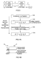
- Fig. 3 illustrates an apparatus for performing a three-operand addition, as indicated in the formula to the right in Fig. 3.
- the three-operand addition is performed by means of a three-bit adder which operates without a carry, ie a half adder, and a two-bit adder downstream, which works with carry, ie which is a full adder.
- a three-bit adder which operates without a carry, ie a half adder, and a two-bit adder downstream, which works with carry, ie which is a full adder.
- Fig. 3 shows a so-called bit-slice of such adder.
- three numbers with, for example 1024 binary digits would be the arrangement shown in FIG for a fully parallel operation 1024 times in the arithmetic Unit of an arithmetic unit 106 may be present.
- each sub-computer 106 to 112 (FIG. 1) is arranged, to a modular multiplication using the Look-ahead algorithm to execute, in DE 36 31 992 C2 is set forth.
- a required modular multiplication is based on of Fig. 4b explained. It is the task of the binary numbers Multiply "111" and "101" with each other. For this purpose, this multiplication becomes analogous in a partial calculation a multiplication of two numbers according to the known "Schulmathematik" executed, but with binary number representation. Due to the simplicity of illustration will be below the case considered in which no look-ahead algorithm and no modulo reduction is used. If this algorithm is performed, it results first a first partial product "111". This partial product becomes then, to take into account its significance to a position moved to the left. To the first shifted to the left Partial product, as an intermediate result of a first iteration step then, in one second iteration step the second partial product "000" added.
- the multiplicand M represents the partial product if the considered location of the multiplier is a binary "1".
- the partial product is 0 if the considered position of the multiplier is a binary "0".
- the positions or the valences of the partial products are taken into account by the respective displacement operations. In Fig. 4b this is represented by the offset application of the partial products.
- two registers Z 1 and Z 2 are required for the addition of FIG. 4 b. The first partial product could be stored in register Z 1 and then shifted one bit to the left in this register. The second partial product could be stored in register Z 2 . The subtotal could then be stored again in the register Z 1 and then pushed back one bit to the left. The third partial product would be stored again in register Z 2 . The final result would then be in register Z 1 .
- FIG. 4a A schematic flow diagram for the method shown in FIG. 4b can be found in FIG. 4a.
- a step S10 the registers present in a part processor are initialized.
- a step S12 after initialization, a three-operand addition is performed to calculate the first partial product.
- the equation denoted in FIG. S12 would comprise only Z, a 1 and P 1 .
- a 1 can be referred to as the first look-ahead parameter.
- a has a value of "1" if the considered location of the multiplier O is a 1.
- a is equal to zero if the considered digit of the multiplier is a zero.
- step S12 The operation shown in block S12 becomes parallel to all for example, 1024 bits performed. Thereupon will be in a step S14 in the simplest case, a shift operation performed by one position to the right to take into account that the most significant bit of the 2nd partial product one digit lower than the most significant one Bit of the 1st partial product. Have several consecutive Bits of the multiplier O a zero, so finds one Shift by several positions to the right instead. Finally, in a step S16, the parallel again Three-operand addition, for example, using the in Fig. 3 adder chain performed.
- Serial / Parallel means ie the parallel implementation in the block S12 or S16, and serial processing to successively all partial products to combine with each other.
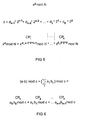
- FIG. 5 The operation x d mod N is considered in FIG. 5.
- the exponent d is represented in binary notation.
- FIG. 5 this results in a chain of modular multiplications, wherein, as also shown in FIG. 5, each modular single operation can each be assigned to a sub-calculator, such that all modular operations are performed in parallel by the one described in FIG 1 cryptography processor shown are executed.
- the intermediate results then obtained, after having been determined in parallel, are multiplied up to obtain the result.
- the control unit 105 controls the division into the individual partial calculation units TRW 1 to TRW k and then the final Aufmultipliring the individual intermediate results.
- FIG. 6 shows another example of a division of an operation (a * b) mod c into a plurality of modular operations.
- the partial calculator TRW 1 can determine a first intermediate result.
- the partial calculators TRW 2 to TRW n also calculate intermediate results, whereupon, after receiving the intermediate results, the control unit 105 controls the multiplication of the intermediate results.
- the control unit controls the summation z. B. so that it selects a partial calculation, which then receives the intermediate results for summation.
- an operation is split into several independent sub-operations.
- FIGS. 5 and 6 serve only to illustrate the possibilities for division an operation in a plurality of sub-operations, wherein quite favorable divisions in terms of achievable Performance can exist.
- Essential to the examples is therefore not the performance of the processor, but that divisions exist, so that each partial calculation one performs independent sub-operation, and that a plurality controlled by sub-operations of a control unit is to create a veiled current profile at the power input to get into the chip.
Landscapes
- Engineering & Computer Science (AREA)
- Theoretical Computer Science (AREA)
- Physics & Mathematics (AREA)
- Software Systems (AREA)
- General Physics & Mathematics (AREA)
- General Engineering & Computer Science (AREA)
- Computer Hardware Design (AREA)
- Mathematical Physics (AREA)
- Computer Security & Cryptography (AREA)
- Pure & Applied Mathematics (AREA)
- Mathematical Analysis (AREA)
- Mathematical Optimization (AREA)
- Computational Mathematics (AREA)
- Computing Systems (AREA)
- Computer Networks & Wireless Communication (AREA)
- Signal Processing (AREA)
- Advance Control (AREA)
- Storage Device Security (AREA)
- Multi Processors (AREA)
- Power Sources (AREA)
- Microcomputers (AREA)
- Bidet-Like Cleaning Device And Other Flush Toilet Accessories (AREA)
- Preparation Of Compounds By Using Micro-Organisms (AREA)
- Devices For Executing Special Programs (AREA)
- Saccharide Compounds (AREA)
Abstract
Description
Die vorliegende Erfindung bezieht sich auf Kryptographietechniken und insbesondere auf die Architektur von für kryptographische Anwendungen verwendeten Kryptographieprozessoren.The present invention relates to cryptographic techniques and in particular on the architecture of cryptographic Applications used cryptographic processors.
Mit zunehmender Verbreitung von bargeldlosem Zahlungsverkehr, elektronischer Datenübertragung über öffentliche Netze, Austausch von Kreditkartennummern über öffentliche Netze und allgemein gesagt der Verwendung von sogenannten Smart Cards für Zahlungs-, Identifikations- oder Zugriffszwecke entsteht ein immer größerer Bedarf nach Kryptographietechniken. Kryptographietechniken umfassen einerseits Kryptographiealgorithmen und andererseits geeignete Prozessorenlösungen, welche die durch die Kryptographiealgorithmen vorgeschriebenen Berechnungen ausführen. Wurden früher Kryptographiealgorithmen mit Allzweckrechnern ausgeführt, so spielten die Kosten, der Rechenzeitbedarf und die Sicherheit gegenüber verschiedenartigsten Fremdattacken keine derart entscheidende Rolle wie heutzutage, wo kryptographische Algorithmen immer mehr auf Chipkarten oder speziellen Sicherheits-ICs ausgeführt werden, für die besondere Anforderungen gelten. So müssen solche Smart Cards einerseits preisgünstig verfügbar sein, da sie Massenprodukte sind, andererseits jedoch eine große Sicherheit gegenüber Fremdattacken aufweisen, da sie vollständig in der Gewalt des potentiellen Angreifers sind.With the spread of cashless payments, electronic data transmission over public networks, exchange of credit card numbers over public networks and Generally speaking, the use of so-called smart cards for payment, identification or access purposes an ever-increasing need for cryptographic techniques. cryptography techniques on the one hand include cryptographic algorithms and on the other hand, suitable processor solutions which the computations prescribed by the cryptographic algorithms To run. Were earlier cryptographic algorithms running with general purpose computers, so did the cost, the Computing time and security against most varied Foreign attacks do not play such a decisive role as nowadays, where cryptographic algorithms are more and more on Smart cards or special security ICs are executed, for which special requirements apply. Such must be Smart cards on the one hand be reasonably priced, as they are However, mass products are, on the other hand, a great security against external attacks, since they are completely in the power of the potential attacker.
Darüber hinaus müssen kryptographische Prozessoren eine beachtliche Rechenleistung zur Verfügung stellen, zumal die Sicherheit von vielen kryptographischen Algorithmen, wie z. B. dem bekannten RSA-Algorithmus, entscheidend von der Länge der verwendeten Schlüssel abhängt. In anderen Worten ausgedrückt bedeutet dies, dass mit zunehmender Länge der zu verarbeitenden Zahlen auch die Sicherheit ansteigt, da ein Angriff, der auf dem Ausprobieren aller Möglichkeiten basiert, aus Rechenzeitgründen unmöglich gemacht wird.In addition, cryptographic processors have a considerable Provide computing power, especially the security many cryptographic algorithms such. B. the well-known RSA algorithm, crucial on the length of the used key depends. In other words this means that with increasing length of the processed Numbers also increase security, as an attack that based on trying out all possibilities, for calculation time reasons is made impossible.
In Zahlenwerten ausgedrückt bedeutet dies, dass Kryptographieprozessoren mit Integers, d. h. Ganzzahlen, umgehen müssen, welche eine Länge von vielleicht 1024 Bits, 2048 Bits oder vielleicht sogar noch mehr haben können. Zum Vergleich verarbeiten Prozessoren in einem üblichen PC 32-Bit- bzw. 64-Bit-Ganzzahlen.Expressed in numerical terms, this means that cryptographic processors with Integers, d. H. Integers, have to deal which may have a length of perhaps 1024 bits, 2048 bits or maybe even more. For comparison Processors in a standard PC handle 32-bit and 64-bit integers, respectively.
Ein hoher Rechenaufwand bedeutet jedoch auch eine hohe Rechenzeit, so dass für Kryptographieprozessoren gleichzeitig auch die wesentliche Anforderung darin besteht, einen hohen Rechendurchsatz zu erreichen, damit beispielsweise eine Identifikation, ein Zugang zu einem Gebäude, eine Bezahlungstransaktion oder eine Kreditkartenübermittlung nicht viele Minuten dauert, was für die Marktakzeptanz sehr schädlich wäre.However, a high computational effort also means a high computing time, so for cryptography processors at the same time also the essential requirement is a high Computer throughput, so that, for example, an identification, an access to a building, a payment transaction or a credit card transfer not many Minutes, which would be very damaging for the market acceptance.
Zusammenfassend lässt sich daher feststellen, dass Kryptographieprozessoren sicher, schnell und daher außerordentlich leistungsstark sein müssen.In summary, it can be concluded that cryptography processors safe, fast and therefore extraordinary have to be powerful.
Eine Möglichkeit, um den Durchsatz durch einen Prozessor zu
erhöhen, besteht darin, eine zentrale Verarbeitungseinheit
mit einem oder mehreren Coprozessoren, welche parallel arbeiten,
auszustatten, wie es beispielsweise bei modernen PCs oder
aber auch bei modernen Graphikkarten der Fall ist. Ein
solches Szenario ist in Fig. 7 gezeigt. Fig. 7 zeigt eine
Computerplatine 800, auf der eine CPU 802, ein Arbeitsspeicher
(RAM) 804, ein erster Coprozessor 806, ein zweiter Coprozessor
808 sowie ein dritter Coprozessor 810 angeordnet
sind. Die CPU 802 ist mit den drei Coprozessoren 806, 808,
810 über einen Bus 812 verbunden. Ferner kann für jeden Coprozessor
ein eigener Speicher vorgesehen sein, welcher nur
für Operationen des Coprozessors dient, d. h. ein Speicher 1
814, ein Speicher 2 816 für den Coprozessor 2 sowie ein Speicher
3 818 für den Coprozessor 3.One way to increase throughput through a processor
increase, is a central processing unit
with one or more coprocessors working in parallel,
equip it, as it does for example with modern PCs or
but also in modern graphics cards is the case. One
such scenario is shown in FIG. Fig. 7 shows a
Ferner wird jeder Chip, der auf der in Fig. 7 gezeigten Computerplatine
800 angeordnet ist, über einen eigenen Strom-
bzw. Spannungsversorgungsanschluss I1 bis I8 mit der für das
Funktionieren der elektronischen Komponenten innerhalb der
einzelnen Elemente benötigten elektrischen Leistung versorgt.
Für die Platine kann alternativ auch nur eine Stromversorgung
vorhanden sein, die dann über die Platine zu den einzelnen
Chips auf der Platine verteilt wird. Dabei stehen jedoch die
Versorgungsleitungen zu den einzelnen Chips für einen Angreifer
zur Verfügung.Further, each chip disposed on the
Das in Fig. 7 gezeigte Konzept für übliche Computeranwendungen ist aus mehreren Gründen für Kryptographieprozessoren ungeeignet. Zum einen sind alle Elemente für die Kurzzahl-Arithmetik aufgeführt, während Kryptographieprozessoren Langzahlarithmetik-Operationen durchführen müssen.The concept shown in Fig. 7 for common computer applications is unsuitable for cryptographic processors for several reasons. For one thing, all elements are for short-number arithmetic while cryptography processors perform long-range arithmetic operations have to perform.
Des weiteren weist jeder Chip auf der Computerplatine 800 einen
eigenen Strom- bzw. Leistungszugang auf, auf den ohne
weiteres von einem Angreifer zugegriffen werden kann, um
Leistungsprofile oder Stromprofile über der Zeit abzugreifen.
Das Abgreifen von Leistungsprofilen über der Zeit ist die Basis
für eine Vielzahl von effizienten Attacken gegenüber
Kryptographieprozessoren. Weitere Hintergründe bzw. eine detaillierte
Darstellung verschiedener Attacken gegen Kryptographieprozessoren
sind in "Information Leakage Attacks A-gainst
Smart Card Implementations of Cryptographic Algorithms
and Countermeasures", Hess u. a., Eurosmart Security Conference,
13. Juni bis 15. Juni 2000, dargestellt. Als Gegenmaßnahmen
werden Implementationen vorgeschlagen, welche darauf
aufbauen, dass verschiedene Operationen immer die gleiche
Zeit benötigen, so dass ein Angreifer aufgrund eines Leistungsprofils
nicht ersehen kann, ob der Kryptoprozessor eine
Multiplikation, eine Addition oder irgend etwas anderes ausgeführt
hat.Furthermore, each chip on the
In "Design of Long Integer Arithmetic units for Public-Key Algorithms", Hess u. a. Eurosmart Security Conference, 13. Juni bis 15. Juni 2000 wird auf verschiedene Rechenoperationen eingegangen, welche von Kryptographie-Prozessoren ausführbar sein müssen. Insbesondere wird auf die modulare Multiplikation, Verfahren zur modularen Reduktion sowie auf das sogenannten ZDN-Verfahren eingegangen, das in dem deutschen Patent DE 36 31 992 C2 dargestellt ist.In "Design of Long Integer Arithmetic units for Public-Key Algorithms ", Hess and others Eurosmart Security Conference, 13. June to June 15, 2000 will be on various arithmetic operations which can be executed by cryptography processors have to be. In particular, the modular multiplication, Method for modular reduction and on the so-called ZDN method, which in the German Patent DE 36 31 992 C2 is shown.
Das ZDN-Verfahren basiert auf einer Seriell/Parallel-Architektur unter Verwendung von parallel ausführbaren Look-Ahead Algorithmen für die Multiplikation und die modulare Reduktion, um eine Multiplikation zweier Binärzahlen in eine iterative 3-Operanden-Addition unter Verwendung von Look-Ahead-Parametern für die Multiplikation und die modulare Reduktion zu transformieren. Hierzu wird die modulare Multiplikation in eine serielle Berechnung von Partialprodukten zerlegt. Zu Beginn der Iteration werden zwei Partialprodukte gebildet und dann unter Berücksichtigung der modularen Reduktion zusammenaddiert, um ein Zwischenergebnis zu erhalten. Hierauf wird ein weiteres Partialprodukt gebildet und wieder unter Berücksichtigung der modularen Reduktion zu dem Zwischenergebnis hinzuaddiert. Diese Iteration wird fortgesetzt, bis sämtliche Stellen des Multiplikators abgearbeitet sind. Für die Drei-Operanden-Addition umfasst ein Kryptocoprozessor ein Addierwerk, welches in einem aktuellen Iterationsschritt die Summation eines neuen Partialprodukts zu dem Zwischenergebnis des vorausgehenden Iterationsschritts durchführt.The ZDN method is based on a serial / parallel architecture using parallel executable look-ahead Algorithms for multiplication and modular reduction, by a multiplication of two binary numbers into one iterative 3-operand addition using look-ahead parameters for multiplication and modular reduction to transform. This is the modular multiplication decomposed into a serial calculation of partial products. At the beginning of the iteration, two partial products are formed and then taking into account the modular reduction added together to get an intermediate result. Then another partial product is formed and again taking into account the modular reduction to the intermediate result added. This iteration continues until all parts of the multiplier have been processed. For the three-operand addition involves a crypto-coprocessor an adder, which is in a current iteration step the summation of a new partial product to the intermediate result of the preceding iteration step.
So könnte jeder Coprozessor von Fig. 7 mit einer eigenen ZDN-Einheit ausgestattet sein, um mehrere modulare Multiplikationen parallel auszuführen, um für bestimmte Anwendungen den Durchsatz zu erhöhen. Diese Lösung würde jedoch wiederum daran scheitern, dass ein Angreifer von jedem Chip einzeln die Stromprofile eruieren könnte, so dass zwar eine Erhöhung des Durchsatzes erreicht worden ist, jedoch auf Kosten der Sicherheit des Kryptographie-Rechners.Thus, each coprocessor of FIG. 7 could have its own ZDN unit be equipped to several modular multiplications run parallel to the for certain applications Increase throughput. However, this solution would turn on it fail that an attacker of each chip individually the Could elicit power profiles, so that although an increase in the Throughput has been achieved, but at the expense of security of the cryptography calculator.
Die Aufgabe der vorliegenden Erfindung besteht darin, einen schnellen und sicheren Kryptographieprozessor zu schaffen.The object of the present invention is to provide a fast and secure cryptography processor.
Diese Aufgabe wird durch einen Kryptographieprozessor nach
Patentanspruch 1 gelöst.This task is followed by a
Der vorliegenden Erfindung liegt die Erkenntnis zugrunde, dass ein schneller Kryptographieprozessor nur erreicht werden kann, wenn eine Kryptographie-Rechenoperation in mehrere Teiloperationen zerlegt wird, und diese Teiloperationen von parallel angeordneten Teilrechenwerken ausgeführt werden. Andererseits kann eine Sicherheit insbesondere gegen Leistungsabhörattacken nur erreicht werden, wenn sämtliche Teilrechenwerke einschließlich der Steuereinheit für die Teilrechenwerke und der zentralen Verarbeitungseinheit auf einem einzigen Chip angeordnet werden, so dass die Leistungszugänge für die einzelnen Komponenten nicht für einen äußeren Angreifer zur Verfügung stehen.The present invention is based on the knowledge that a fast cryptography processor can only be achieved can, if a cryptographic compute operation in several Partial operations is decomposed, and these sub-operations of be executed parallel part calculations. on the other hand can be a security especially against performance monitoring attacks can only be achieved if all sub-calculators including the control unit for the sub-processors and the central processing unit on a single Chip can be arranged so that the power inputs for the individual components not for an external attacker To be available.
Anders ausgedrückt sind die zentrale Verarbeitungseinrichtung und der Coprozessor, der eine einzige Steuereinheit sowie die Mehrzahl von Teilrechenwerken aufweist, auf einem einzigen Chip integriert. Darüber hinaus weist dieser einzige Chip lediglich einen einzigen Versorgungszugang zum Versorgen der Mehrzahl von Teilrechenwerken, der Steuereinheit und der zentralen Verarbeitungseinheit mit Strom auf.In other words, the central processing facility and the coprocessor, which has a single control unit as well Has a plurality of sub-calculations, on a single Integrated chip. In addition, this single chip only has a single supply access to supply the A plurality of sub-processors, the control unit and the central processing unit with power on.
Das Integrieren dieser Komponenten auf einem Chip und das Versorgen des Chips mit einem Versorgungsstromzugang hat den Vorteil, dass sich am Stromanschluss des Kryptographieprozessors die Stromprofile, die den Operationen der Teilrechenwerke zugeordnet sind, überlagern. Wenn beispielsweise zwei Teilrechenwerke parallel arbeiten, so überlagern sich die Stromprofile dieser beiden Teilrechenwerke, derart, dass es für den Angreifer schwierig wird, anhand des Leistungsversorgungsprofils zu erkennen, welche Operationen mit welchen Zahlen die beiden Teilrechenwerke gleichzeitig durchführen. Wird die Anzahl der Teilrechenwerke erhöht, so wird auch das Stromprofil an dem einzigen Versorgungsanschluss immer homogener. Durch zunehmende parallele Verarbeitung mit zunehmender Anzahl von parallelen Teilrechenwerken steigt jedoch auch der Durchsatz, so dass sich beim erfindungsgemäßen Konzept mit zunehmendem Durchsatz auch die Sicherheit erhöht. Im Stand der Technik war dies nicht der Fall, ganz im Gegenteil verringerte sich die Sicherheit mit zunehmendem Durchsatz.Integrating these components on a chip and that Providing the chip with a supply stream access has that Advantage that is at the power connector of the cryptographic processor the electricity profiles, the operations of the partial calculators are superimposed. For example, if two Partial calculators work in parallel, so superimpose the Power profiles of these two sub-calculations, such that it becomes difficult for the attacker, based on the power supply profile to recognize which operations with what numbers perform the two partial calculations simultaneously. Becomes the number of partial calculators increases, so does the Current profile at the single supply connection increasingly homogeneous. Due to increasing parallel processing with increasing However, the number of parallel part calculations is also increasing the throughput, so that in the inventive concept Increases security with increasing throughput. in the The state of the art was not the case, quite the opposite Safety decreased with increasing throughput.
Eine Grenze der parallelen Verarbeitung ist dann erreicht, wenn der Rechenaufwand in der Steuereinheit zum Verteilen der Teiloperationen auf die Teilrechenwerke und zum Ansteuern der einzelnen Teilrechenwerke stark zunimmt. Für relativ lang dauernde Operationen, wie z. B. die Multiplikation von zwei sehr langen Ganzzahlen, ist jedoch das Verhältnis von Rechenzeit in einem Teilrechenwerk zu der Rechenzeit der Steuereinheit für Organisations- und Verwaltungsaufgaben so groß, dass ein beachtlicher Grad an Parallelität erreicht werden kann, ohne dass der Verwaltungsaufwand in problematische Größenordnungen kommt.A limit of parallel processing is then reached if the computational effort in the control unit to distribute the Sub-operations on the sub-processors and for driving the individual part of the calculation increases sharply. For a relatively long time continuous operations, such as B. the multiplication of two very long integers, however, is the ratio of computation time in a partial calculation to the computing time of the control unit so great for organizational and administrative tasks that a considerable degree of parallelism can be achieved without the administrative burden in problematic scales comes.
Dieser Grad an Parallelität ist jedoch nötig, um den Durchsatz so weit zu erhöhen, dass Geschwindigkeitsverluste der Logikeinheiten ausgeglichen werden können, welche auftreten, wenn sowohl Logikbausteine als auch Speicherbausteine auf demselben Chip integriert werden. Allgemein besteht die Bestrebung, Logikbausteine und Speicherbausteine auf getrennten Chips anzuordnen, da sich die Technologien für diese beiden Bauelemente unterscheiden. Anders ausgedrückt erlaubt eine Speicher-Technologie, mit der Logikbausteine hergestellt werden, keine so schnellen Logikbausteine, als wenn die Logikbausteine mit einer speziell für Logikbausteine angepassten Technologie hergestellt werden. Daher sind bei dem in Fig. 7 gezeigten Beispiel der einfachen Parallelschaltung verschiedener Coprozessoren immer Speicher und Rechenwerke auf getrennten Bausteinen implementiert.However, this degree of parallelism is necessary to the throughput so far that speed losses of the Logic units can be balanced, which occur if both logic modules and memory modules on integrated into the same chip. There is a general desire to Logic blocks and memory blocks on separate Arrange chips as the technologies for these two Distinguish components. In other words, one allows Memory technology used to make logic devices no logic blocks as fast as the logic blocks with a specially adapted for logic devices Technology can be produced. Therefore, in the case of FIG. 7 shown example of simple parallel connection of various Coprocessors always store and arithmetic on separate Implemented blocks.
Für eine hohe Sicherheit ist es jedoch gerade wichtig, dass ein Angreifer nicht die Kommunikation zwischen einem Rechenwerk und einem Register abhören kann.However, for a high level of security, it is important that An attacker does not communicate between an arithmetic unit and listen to a register.
Bevorzugte Ausführungsbeispiele der vorliegenden Erfindung werden nachfolgend bezugnehmend auf die beiliegenden Zeichnungen detailliert erläutert. Es zeigen:
- Fig. 1
- einen erfindungsgemäßen Kryptoprozessor, der auf einem einzigen Chip integriert ist;
- Fig. 2
- eine detailliertere Darstellung des Coprozessors, welcher verschiedene Teilrechenwerke mit unterschiedlich langen Registern aufweist;
- Fig. 3
- eine detailliertere Darstellung einer Arithmetikeinheit, welche für eine Drei-Operanden-Addition geeignet ist;
- Fig. 4a
- ein schematisches Flussdiagramm zum Durchführen einer modularen Multiplikation auf seriell/parallele Art und Weise;
- Fig. 4b
- ein Zahlenbeispiel zur Veranschaulichung der seriell/parallelen Arbeitsweise einer Arithmetikeinheit am Beispiel einer Multiplikation;
- Fig. 5
- ein Beispiel zum Aufteilen einer modularen Exponentiation in eine Anzahl von modularen Multiplikationen;
- Fig. 6
- ein weiteres Beispiel zum Aufteilen einer modularen Multiplikation auf verschiedene Teilrechenwerke; und
- Fig. 7
- eine Computerplatine mit einer Vielzahl von getrennt versorgten Bauelementen.
- Fig. 1
- a cryptoprocessor according to the invention, which is integrated on a single chip;
- Fig. 2
- a more detailed representation of the coprocessor, which has different sub-calculators with different length registers;
- Fig. 3
- a more detailed representation of an arithmetic unit which is suitable for a three-operand addition;
- Fig. 4a
- a schematic flow diagram for performing a modular multiplication in a serial / parallel manner;
- Fig. 4b
- a numerical example to illustrate the serial / parallel operation of an arithmetic unit using the example of a multiplication;
- Fig. 5
- an example of dividing a modular exponentiation into a number of modular multiplications;
- Fig. 6
- another example of dividing a modular multiplication into different sub-computations; and
- Fig. 7
- a computer board with a plurality of separately powered components.
Bevor detaillierter auf die einzelnen Figuren eingegangen wird, wird im nachfolgenden ausgeführt, weshalb durch Parallelschaltung mehrerer Teilrechenwerke, die auf einem Chip angeordnet sind und durch eine Steuereinheit, die auf demselben Chip angeordnet ist, gesteuert werden, eine höhere Sicherheit erreicht wird.Before going into more detail on the individual figures will be explained below, which is why connected in parallel several sub-calculators arranged on a chip are and by a control unit that is on the same Chip is arranged, controlled, higher security is reached.
Kryptoprozessoren werden für sicherheitskritische Anwendung benutzt, beispielsweise für digitale Signaturen, Authentifikationen oder Verschlüsselungsaufgaben. Ein Angreifer möchte beispielsweise den geheimen Schlüssel herausfinden, um dadurch das Kryptographieverfahren zu brechen. Kryptographie-prozessoren werden beispielsweise in Chipkarten eingesetzt, welche, wie es bereits ausgeführt worden ist, Smart Cards oder Signaturkarten für eine rechtsverbindliche elektronische Unterschrift oder auch für Homebanking oder zum Bezahlen mit dem Mobiltelephon usw. umfassen. Alternativ werden solche Kryptoprozessoren auch in Computern und Servern als Sicherheits-IC eingesetzt, um eine Authentifikation durchzuführen, oder um Verschlüsselungsaufgaben wahrnehmen zu können, welche beispielsweise im sicheren Bezahlen über das Internet, in sogenannten SSL-Sessions (SSL = Secure Socket Layer), d. h. der sicheren Übermittlung von Kreditkartennummern, bestehen können.Cryptoprocessors are used for safety-critical applications used, for example, for digital signatures, authentications or encryption tasks. An attacker wants For example, find out the secret key to thereby to break the cryptography process. Cryptographic processors are used for example in chip cards, which, as has already been stated, smart cards or Signature cards for a legally binding electronic Signature or for home banking or to pay with the mobile phone, etc. Alternatively, such Crypto processors also in computers and servers as a security IC used to perform an authentication, or to be able to perform encryption tasks, which, for example, in secure payment via the Internet, in so-called SSL sessions (SSL = Secure Socket Layer), d. H. secure transmission of credit card numbers can.
Typische physikalische Angriffe messen den Stromverbrauch (SPA, DPA, Timing-Attacken) oder die elektromagnetische Abstrahlung. Bezüglich einer näheren Erläuterung der Angriffe sei auf die eingangs erwähnten Literaturstellen verwiesen. Typical physical attacks measure power consumption (SPA, DPA, timing attacks) or the electromagnetic radiation. For a more detailed explanation of the attacks reference is made to the references mentioned above.
Da die Angreifer bei der heutigen Halbleitertechnologie, welche Strukturen im Bereich von typischerweise kleiner oder gleich 250 Nanometern erreicht, nur sehr schwer lokale Strommessungen durchführen können, wird bei einem Angriff typischerweise der Stromverbrauch der gesamten Chipkarte einschließlich CPU und Coprozessor gemessen, welcher sich aus der Summe der einzelnen Stromverbräuche von beispielsweise der CPU, dem RAM, einem ROM, einem E2PROM, einem Flash-Memory, einer Zeitsteuereinheit, einem Zufallszahlengenerator (RNG), einem DES-Modul und dem Kryptocoprozessor zusammensetzt.Since today's semiconductor technology, which achieves structures in the range of typically less than or equal to 250 nanometers, makes attackers very difficult to carry out local current measurements, an attack typically measures the power consumption of the entire chip card, including the CPU and coprocessor, which is the sum of the individual power consumptions of, for example, the CPU, the RAM, a ROM, an E 2 PROM, a flash memory, a timing controller, a random number generator (RNG), a DES module, and the crypto-coprocessor.
Da der Kryptocoprozessor typischerweise den größten Stromverbrauch hat, kann ein Angreifer sehen, wann der Kryptocoprozessor zu rechnen beginnt. Um dies zu vermeiden, wäre ein über der Zeit vollständig konstanter Stromverbrauch das Ziel, ein Angreifer würde dann nicht mehr erkennen, wann der Kryptocoprozessor zu rechnen beginnt. Dieses ideale Ziel kann nicht erreicht werden, es wird jedoch durch das erfindungsgemäße Parallelschalten von Teilrechenwerken ein möglichst gleichförmiges "Rauschen" um einen Mittelwert angestrebt.Because the crypto-coprocessor typically consumes the most power an attacker can see when the crypto coprocessor begins to count. To avoid this would be a completely constant power consumption over time Target, an attacker would then no longer recognize when the Crypto coprocessor begins to count. This ideal destination can can not be achieved, but it is by the inventive Parallel switching of partial calculations as possible uniform "noise" aimed at a mean value.
Der Stromverbrauch eines beispielsweise in CMOS-Technologie gefertigten Chips ändert sich bei einer Umschaltung von einer "0" auf eine "1". Daher ist der Stromverbrauch datenabhängig sowie abhängig von den verwendeten Befehlen der CPU und des Kryptocoprozessors.The power consumption of an example in CMOS technology manufactured chips changes when switching from one "0" to a "1". Therefore, the power consumption is data dependent as well as the used commands of the CPU and the Cryptocoprocessor.
Schaltet man nun mehrere Teilrechenwerke parallel und lässt sie mehrere Operationen bzw. Teiloperationen parallel abarbeiten, oder wird eine Operation auf mehrere Teilrechenwerke aufgeteilt, so überlagern sich, wie es ausgeführt worden ist, die Stromprofile, welche durch die Daten- und Befehlsverarbeitung entstehen.If you now switch several sub-algorithms in parallel and leaves they process several operations or sub-operations in parallel, or will an operation on multiple sub-calculators split up, as it has been stated overlay the power profiles generated by the data and command processing arise.
Je mehr Teilrechenwerke parallel arbeiten, desto schwieriger kann auf Daten und Befehle in den einzelnen Teilrechenwerken bzw. in der Steuereinheit zurückgeschlossen werden, da die Daten und Befehle in jedem Teilrechenwerk üblicherweise unterschiedlich sein werden, der Angreifer jedoch nur die Überlagerung unterschiedlicher Befehle sieht.The more sub-processors work in parallel, the more difficult can access data and commands in each sub-calculation or be deduced in the control unit, as the Data and commands in each sub-computer usually differ but the attacker will only be overlaying sees different commands.
Fig. 1 zeigt einen erfindungsgemäßen Kryptoprozessor zum
Durchführen von Operationen für kryptographische Anwendungen.
Der Kryptoprozessor ist auf einem einzigen Chip 100 implementiert
und umfasst eine zentrale Verarbeitungseinheit (CPU)
102 und einen Coprozessor 104. Der Coprozessor 104 ist, wie
es in Fig. 1 gezeigt ist, auf demselben Chip angeordnet wie
die zentrale Verarbeitungseinheit 102. Der Coprozessor umfasst
eine Mehrzahl von Teilrechenwerken 106, 108, 110 und
112, wobei jedes Teilrechenwerk 106 bis 112 eine eigene arithmetische
Einheit AU aufweist. Vorzugsweise umfasst jedes
Teilrechenwerk 106 bis 112 neben der AU auch zumindest ein
Register (REG), um, wie es bezugnehmend auf Fig. 2 ausgeführt
wird, Zwischenergebnisse speichern zu können.Fig. 1 shows a cryptoprocessor according to the invention for
Performing operations for cryptographic applications.
The crypto processor is implemented on a
Ein typischer Kryptoprozessor wird eine Eingangsschnittstelle
114 und eine Ausgangsschnittstelle 116 umfassen, welche mit
äußeren Anschlüssen für eine Dateneingabe bzw. eine Datenausgabe
sowie mit der CPU 102 verbunden sind. Typischerweise ist
der CPU 102 ein eigener Speicher 118 zugeordnet, der in Fig.
1 mit RAM bezeichnet ist. Unter anderem kann der Kryptoprozessor
noch einen Taktgenerator 120, weitere Speicher, Zufallszahlengeneratoren
etc. umfassen, welche in Fig. 1 nicht
gezeigt sind.A typical crypto processor becomes an
Es sei darauf hingewiesen, dass sämtliche in Fig. 1 dargestellten
Elemente auf einem einzigen Chip implementiert sind,
welcher durch einen einzigen Stromversorgungsanschluss 122
mit Leistung versorgt wird. Der Chip 100 umfasst intern
Stromversorgungsleitungen zu sämtlichen in Fig. 1 gezeigten
Elementen, welche jedoch aus oben angegebenen Gründen nicht
einzeln abgehört werden können. Dagegen stellt es ein Leichtes
dar, den Stromversorgungsanschluss 122 abzuhören. Im Gegensatz
zu der in Fig. 7 gezeigten Platine, bei der die
Stromversorgungsanschlüsse jeder einzelnen Komponente sehr
leicht abhörbar sind, und daher sehr "ausdrucksstarke" Stromprofile
haben, ist das am Stromversorgungsanschluss 122 anliegende
Stromprofil nahezu konstant bzw. weist ein möglichst
homogenes Rauschen um einen konstanten Wert auf. Dies ist
darauf zurückzuführen, dass der Coprozessor 104, welcher am
meisten zum Stromverbrauch beiträgt, eine Mehrzahl von parallel
angeordneten Teilrechenwerken aufweist, die unabhängig
voneinander beispielsweise von "0" auf "1" umschalten und daher
unkorreliert voneinander Strom verbrauchen.It should be noted that all shown in Fig. 1
Elements are implemented on a single chip,
which by a single
Die Parallelschaltung der einzelnen Teilrechenwerke führt zudem dazu, dass der Durchsatz des Kryptonprozessors erhöht werden kann, so dass im Falle der Ausführung eines Speichers auf dem Chip die damit einhergehenden Geschwindigkeitseinbußen, welche aufgrund unterschiedlicher Technologien für Speicher und Rechenwerke auftreten, mehr als ausgeglichen werden können.The parallel connection of the individual sub-calculators also leads to increase the throughput of the krypton processor can be, so in case of execution of a memory on the chip the consequent loss of speed, which due to different technologies for Memory and arithmetic units occur, more than balanced can be.
Gemäß einem bevorzugten Ausführungsbeispiel der vorliegenden
Erfindung können zwei oder mehr Teilrechenwerke als sogenannte
Cluster zusammengefasst werden, derart, dass z. B. ein
erster Cluster Teiloperationen einer ersten Operation durchführt,
während ein zweiter Cluster Teiloperationen einer
zweiten kryptographischen Operation durchführt. So könnte
beispielsweise der erste Cluster, der aus den Teilrechenwerken
106 und 108 besteht, z. B. zwei modulare Exponentiationen
mit jeweils der halben Länge durchführen, welche aus einer
einzigen modularen Exponentiation mit voller Länge hergeleitet
sind, während der zweite Cluster, der aus den Teilrechenwerken
110 und 112 besteht eine modulare Multiplikation
durchführen könnte, wie es in Fig. 6 dargestellt ist.According to a preferred embodiment of the present invention
Invention may be two or more sub-computer as so-called
Clusters are summarized such that z. B. a
first cluster performs partial operations of a first operation,
while a second cluster performs partial operations
performs second cryptographic operation. So could
for example, the first cluster, which consists of the
Alternativ könnte ein Cluster eine RSA-Operation durchführen, während ein anderer Cluster eine DES-Operation durchführt, und wieder ein anderer Cluster beispielsweise eine Hash-Summe berechnet.Alternatively, a cluster could perform an RSA operation, while another cluster performs a DES operation, and another cluster, for example, a hash sum calculated.
An dieser Stelle sei ausgeführt, dass die angesprochenen
Kryptographiealgorithmen in der Literatur bekannt sind und
daher nicht näher ausgeführt werden. Lediglich beispielhaft
sei darauf hingewiesen, dass beispielsweise bei einer RSA-Verschlüsselung
Operanden mit einer Länge von 2048 Bit verarbeitet
werden. Bei der Entschlüsselung ist es mit Hilfe des
chinesischen Restsatzes (CRT) möglich, mit halb so langen Operanden
und zwei Teiloperationen zu arbeiten. Ist ein Kryptographieprozessor
lediglich auf einen solchen Algorithmus
ausgelegt, so beträgt die Anzahl der Teilrechenwerke 2 und
die Länge der arithmetischen Einheiten würde statt 2048 für
eine einzige arithmetische Einheit lediglich 1024 betragen.
Die Teiloperationen gemäß dem chinesischen Restsatz werden
parallel bearbeitet und dann gesteuert durch die Steuereinheit
in einem der beiden Teilrechenwerke kombiniert, um das
Ergebnis zu erhalten.At this point it should be stated that the addressed
Cryptographic algorithms are known in the literature and
therefore not be specified. Merely as an example
it should be noted that, for example, in an RSA encryption
Operands with a length of 2048 bits processed
become. In the decryption it is with the help of the
Chinese remainder theorem (CRT) possible, with half as long operands
and two sub-operations to work. Is a cryptography processor
only to such an algorithm
interpreted, the number of
Fig. 2 zeigt eine detailliertere Darstellung des in Fig. 1
gezeigten Coprozessors 104. Das Teilrechenwerk 106 umfasst
neben der arithmetischen Einheit 106a z. B. drei Register
106b, 106c, 106d. Das Teilrechenwerk 108 umfasst analog dazu
die arithmetische Einheit 108a sowie beispielsweise ebenfalls
drei Register 108b, 108c, 108d. Dasselbe trifft für das Teilrechenwerk
112 zu. Wie es in Fig. 2 gezeigt ist, kann sich
die Länge der Register eines Teilrechenwerks von der Länge
des Registers eines anderen Teilrechenwerks unterscheiden, so
dass beispielsweise mit dem Teilrechenwerk 106 Operationen
mit Zahlen einer Länge L1 durchgeführt werden können, während
mit dem Teilrechenwerk 102 Operationen mit Zahlen einer Länge
L2 durchgeführt werden können.FIG. 2 shows a more detailed representation of the
Die Steuereinheit 105 kann die beiden Teilrechenwerke 106 und
108 beispielsweise auch derart ansteuern, dass die arithmetischen
Einheiten AU1 und AU2 so miteinander verkoppelt werden,
dass beide Teilrechenwerke, welche dann einen Cluster
bilden, arithmetische Operationen mit Zahlen einer Länge L1 +
L2 durchführen. Die Register der beiden Teilrechenwerke können
somit zusammengeschaltet werden.The
Alternativ kann einem Teilrechenwerk jedoch auch eine Anzahl von Registern exklusiv zugewiesen werden, welche so groß ist, dass die Operanden für mehrere Teiloperationen, wie z. B. modulare Multiplikationen oder modulare Exponentiationen, ausreichen. Zur Vermeidung von Informationslecks können die Teiloperationen dann beispielsweise durch eine Einrichtung zum Variieren der Reihenfolge derselben, die in Fig. 2 mit 200 bezeichnet ist, überlagert oder sogar zufällig vermischt werden, um noch eine weitere Verschleierung des Stromprofils zu erreichen. Dies wird besonders dann vorteilhaft sein, wenn beispielsweise lediglich zwei Teilrechenwerke vorhanden sind bzw. lediglich zwei Teilrechenwerke arbeiten, während die anderen Teilrechenwerke eines Kryptographieprozessors gerade stillstehen.Alternatively, however, a number of calculation units can also have a number to be assigned exclusively by registers which is so big that the operands for several sub-operations, such. B. modular Multiplications or modular exponentiations. To avoid information leakage, the Sub-operations then, for example, by a device for varying the order of the same, in Fig. 2 with 200, superimposed or even mixed at random to further obscure the current profile to reach. This will be especially beneficial if For example, only two partial calculators are available or only two sub-processors work while the others Partial processors of a cryptography processor just stand still.
Gemäß einem bevorzugten Ausführungsbeispiel der vorliegenden
Erfindung umfasst die Steuereinheit 105 ferner eine in Fig. 2
nicht gezeigte Einrichtung zum Abschalten von Teilrechenwerken
bzw. Registern von Teilrechenwerken, wenn dieselben nicht
benötigt werden, was besonders für batteriebetriebene Anwendungen
von Vorteil sein kann, um den Stromverbrauch der Gesamt-Schaltung
zu sparen. CMOS-Bauelemente benötigen zwar nur
signifikant Strom, wenn umgeschaltet wird, sie haben jedoch
auch einen Ruhestromverbrauch, welcher dann ins Gewicht fallen
kann, wenn die zur Verfügung stehende Leistung begrenzt
ist.According to a preferred embodiment of the present invention
In the invention, the
Wie es bereits ausgeführt worden ist, hat ein Kryptoprozessor aufgrund der langen Zahlen, die er verarbeiten muss, die Eigenschaft, dass bestimmte Teiloperationen, wie z. B. eine Seriell/Parallel-Multiplikation, wie sie bezugnehmend auf die Fig. 4a und 4b dargestellt wird, ziemlich viel Zeit benötigt. As it has already been stated, has a crypto processor because of the long numbers he has to process, the property that certain sub-operations, such. B. a serial / parallel multiplication, as they are referring to the Fig. 4a and 4b is shown, quite a lot of time needed.
Bevorzugterweise sind die Teilrechenwerke derart ausgeführt,
dass sie eine solche Teiloperation selbständig ohne Eingriffe
der Steuereinheit 105 durchführen können, nachdem die Steuereinheit
den erforderlichen Befehl an das Rechenwerk abgegeben
hat. Hierzu benötigt jedes Teilrechenwerk selbstverständlich
Register zum Speichern der Zwischenlösungen.Preferably, the partial calculations are carried out in such a way
that they do such a sub-operation independently without intervention
the
Aufgrund der Tatsache, dass ein Teilrechenwerk ohne Input der
Steuereinheit 105 relativ lange arbeitet, kann die Steuereinheit
105 eine Vielzahl von einzelnen Teilrechenwerken gewissermaßen
seriell, also nacheinander, mit den nötigen Befehlen
versehen, derart, dass sämtliche Teilrechenwerke parallel arbeiten,
jedoch gewissermaßen gestaffelt zueinander.Due to the fact that a partial calculation without input of
Zum Beispiel wird das erste Teilrechenwerk zu einem bestimmten
Zeitpunkt aktiviert. Ist die Steuereinheit 105 mit der
Aktivierung des ersten Teilrechenwerks fertig, so führt dieselbe
unmittelbar die Aktivierung des zweiten Rechenwerks
durch, während das erste Rechenwerk bereits arbeitet. Das
dritte Teilrechenwerk wird dann aktiviert, wenn die Aktivierung
des zweiten Teilrechenwerks vollendet ist. Dies bedeutet,
dass während der Aktivierung des dritten Teilrechenwerks
das erste und das zweite Teilrechenwerk bereits rechnen. Wenn
dies für alle n Teilrechenwerke durchgeführt wird, so arbeiten
alle Teilrechenwerke zeitlich versetzt. Wenn alle Teilrechenwerke
derart arbeiten, dass ihre Teiloperationen gleich
lang dauern, so wird das erste Teilrechenwerk als erstes fertig
sein. Nun kann die Steuereinheit die Ergebnisse vom ersten
Teilrechenwerk zur zentralen Verarbeitungseinheit übermitteln
und ist mit dieser Übermittlung idealerweise fertig,
bevor das zweite Teilrechenwerk fertig ist. Damit kann der
Durchsatz wesentlich erhöht werden, wobei auch eine optimale
Ausnutzung der Rechenkapazität der Steuereinheit 105 erreicht
wird. Wenn sämtliche Teilrechenwerke identische Operationen
ausführen, so entsteht dennoch ein stark verschleiertes
Stromprofil, da sämtliche Teilrechenwerke zeitlich versetzt
arbeiten. Anders wäre der Fall, wenn sämtliche Teilrechenwerke
durch die Steuereinheit zum gleichen Zeitpunkt aktiviert
werden und gewissermaßen vollständig synchron arbeiten. Dann
würde ein nicht verschleiertes Stromprofil und sogar noch
verstärktes Stromprofil resultieren. Daher ist das serielle
Aktivieren der Teilrechenwerke auch im Hinblick auf die Sicherheit
des Kryptographieprozessors vorteilhaft.For example, the first part of the calculation becomes one
Time activated. Is the
Im nachfolgenden wird auf Fig. 3 eingegangen, welche eine Vorrichtung zum Durchführen einer Drei-Operanden-Addition darstellt, wie sie rechts in Fig. 3 formelmäßig angegeben ist. In der Formel rechts in Fig. 3 ist dargestellt, dass Addition und Subtraktion gleichermaßen ausgeführt werden, da ein Operand einfach mit dem Faktor "-1" multipliziert werden muss, um zu einer Subtraktion zu kommen. Die Drei-Operanden-Addition wird mittels eines Drei-Bit-Addierers, welcher ohne Übertrag arbeitet, d. h. eines Halbaddierers, und eines nachgeschalteten Zwei-Bit-Addierers, durchgeführt, welcher mit Übertrag arbeitet, d. h. welcher ein Volladdierer ist. Alternativ kann auch der Fall auftreten, daß zum Operanden Z nur der Operand N, nur der Operand P oder gar kein Operand hinzuzuaddieren bzw. zu subtrahieren ist. Dies ist in Fig. 3 durch die "Null" unter dem Plus/Minus-Zeichen symbolisiert und wird durch die in Fig. 4a dargestellten sogenannten Look-Ahead-Parameter ai, bi symbolisiert, die in jedem Iterationsschritt erneut berechnet werden.Reference is now made to Fig. 3, which illustrates an apparatus for performing a three-operand addition, as indicated in the formula to the right in Fig. 3. In the formula to the right in FIG. 3 it is shown that addition and subtraction are carried out in the same way, since an operand simply has to be multiplied by the factor "-1" in order to arrive at a subtraction. The three-operand addition is performed by means of a three-bit adder which operates without a carry, ie a half adder, and a two-bit adder downstream, which works with carry, ie which is a full adder. Alternatively, it may also be the case that only the operand N, only the operand P or no operand is to be added or subtracted from the operand Z. This is symbolized in FIG. 3 by the "zero" under the plus / minus sign and is symbolized by the so-called look-ahead parameters a i , b i shown in FIG. 4a, which are recalculated in each iteration step.
Fig. 3 zeigt einen sogenannten Bit-Slice eines solchen Addierwerks.
Für die Addition von drei Zahlen mit beispielsweise
1024 Binärstellen würde die in Fig. 3 gezeigte Anordnung
für einen vollständig parallelen Betrieb 1024 mal in der arithmetischen
Einheit eines Rechenwerks 106 vorhanden sein.Fig. 3 shows a so-called bit-slice of such adder.
For the addition of three numbers with, for example
1024 binary digits would be the arrangement shown in FIG
for a fully parallel operation 1024 times in the arithmetic
Unit of an
Bei einem bevorzugten Ausführungsbeispiel der vorliegenden Erfindung ist jedes Teilrechenwerk 106 bis 112 (Fig. 1) angeordnet, um eine modulare Multiplikation unter Verwendung des Look-Ahead-Algorithmus auszuführen, der in der DE 36 31 992 C2 dargelegt ist. In a preferred embodiment of the present invention Invention, each sub-computer 106 to 112 (FIG. 1) is arranged, to a modular multiplication using the Look-ahead algorithm to execute, in DE 36 31 992 C2 is set forth.
Eine hierfür erforderliche modulare Multiplikation wird anhand von Fig. 4b erläutert. Es besteht die Aufgabe, die Binärzahlen "111" und "101" miteinander zu multiplizieren. Hierzu wird in einem Teilrechenwerk diese Multiplikation analog einer Multiplikation zweier Zahlen gemäß der bekannten "Schulmathematik" ausgeführt, jedoch mit binärer Zahlendarstellung. Aufgrund der Einfachheit der Darstellung wird nachfolgend der Fall betrachtet, in dem kein Look-Ahead-Algorithmus und keine Modulo-Reduktion eingesetzt wird. Wenn dieser Algorithmus durchgeführt wird, so ergibt sich zunächst ein erstes Partialprodukt "111". Dieses Partialprodukt wird dann, um seine Signifikanz zu berücksichtigen, um eine Stelle nach links verschoben. Zu dem ersten nach links verschobenen Partialprodukt, das als Zwischenergebnis eines ersten Iterationsschritts aufgefaßt werden kann, wird dann, in einem zweiten Iterationsschritt das zweite Partialprodukt "000" hinzuaddiert. Das Ergebnis dieser Addition wird dann wieder um eine Stelle nach links verschoben. Das verschobene Ergebnis dieser Addition ist dann das aktualisierte Zwischenergebnis. Zu diesem aktualisierten Zwischenergebnis wird dann das letzte Partialprodukt "111" hinzuaddiert. Das erhaltene Ergebnis ist dann das Endergebnis der Multiplikation. Es ist zu sehen, daß die Multiplikation in zwei Additionen und zwei Verschiebungsoperationen aufgeteilt worden ist.A required modular multiplication is based on of Fig. 4b explained. It is the task of the binary numbers Multiply "111" and "101" with each other. For this purpose, this multiplication becomes analogous in a partial calculation a multiplication of two numbers according to the known "Schulmathematik" executed, but with binary number representation. Due to the simplicity of illustration will be below the case considered in which no look-ahead algorithm and no modulo reduction is used. If this algorithm is performed, it results first a first partial product "111". This partial product becomes then, to take into account its significance to a position moved to the left. To the first shifted to the left Partial product, as an intermediate result of a first iteration step then, in one second iteration step the second partial product "000" added. The result of this addition then becomes again moved one place to the left. The shifted result this addition is then the updated intermediate result. This is the updated intermediate result then the last partial product "111" added. The result obtained is then the final result of the multiplication. It's closed see that multiplication in two additions and two Shift operations has been split.
Es ist ferner zu sehen, daß der Multiplikand M das Partialprodukt darstellt, wenn die betrachtete Stelle des Multiplikators eine binäre "1" ist. Das Partialprodukt ist hingegen 0, wenn die betrachtete Stelle des Multiplikators eine binäre "0" ist. Ferner werden durch die jeweiligen Verschiebungsoperationen die Stellen bzw. die Wertigkeiten der Partialprodukte berücksichtigt. In Fig. 4b ist dies durch das versetzte Auftragen der Partialprodukte dargestellt. Hardwaremäßig werden für die Addition von Fig. 4b zwei Register Z1 und Z2 benötigt. Das erste Partialprodukt könnte in dem Register Z1 gespeichert werden und dann in diesem Register um ein Bit nach links geschoben werden. Das zweite Partialprodukt könnte in dem Register Z2 gespeichert werden. Die Zwischensumme könnte dann wieder im Register Z1 gespeichert werden und dann wieder um ein Bit nach links geschoben werden. Das dritte Partialprodukt würde wieder im Register Z2 gespeichert werden. Das Endergebnis würde dann im Register Z1 stehen.It can also be seen that the multiplicand M represents the partial product if the considered location of the multiplier is a binary "1". By contrast, the partial product is 0 if the considered position of the multiplier is a binary "0". Furthermore, the positions or the valences of the partial products are taken into account by the respective displacement operations. In Fig. 4b this is represented by the offset application of the partial products. In terms of hardware, two registers Z 1 and Z 2 are required for the addition of FIG. 4 b. The first partial product could be stored in register Z 1 and then shifted one bit to the left in this register. The second partial product could be stored in register Z 2 . The subtotal could then be stored again in the register Z 1 and then pushed back one bit to the left. The third partial product would be stored again in register Z 2 . The final result would then be in register Z 1 .
Ein schematisches Flussdiagramm für das in Fig. 4b gezeigte Verfahren findet sich in Fig. 4a. Zunächst werden in einem Schritt S10 die in einem Teilrechenwerk vorhandenen Register initialisiert. In einem Schritt S12 wird anschließend, nach dem Initialisieren, eine Drei-Operanden-Addition durchgeführt, um das erste Partialprodukt zu berechnen. Es sei darauf hingewiesen, dass für das einfache in Fig. 4b gegebene Beispiel, das eine Multiplikation ohne Modulo-Operation darstellt, die in Fig. S12 bezeichnete Gleichung lediglich Z, a1 und P1 umfassen würde. a1 kann als erster Look-Ahead-Parameter bezeichnet werden. In der allereinfachsten Ausführung hat a einen Wert von "1", wenn die betrachtete Stelle des Multiplikators O eine 1 ist. a ist gleich Null, wenn die betrachtete Stelle des Multiplikators eine Null ist.A schematic flow diagram for the method shown in FIG. 4b can be found in FIG. 4a. First, in a step S10, the registers present in a part processor are initialized. Then, in a step S12, after initialization, a three-operand addition is performed to calculate the first partial product. It should be noted that for the simple example given in FIG. 4b, which represents multiplication without modulo operation, the equation denoted in FIG. S12 would comprise only Z, a 1 and P 1 . a 1 can be referred to as the first look-ahead parameter. In the simplest embodiment, a has a value of "1" if the considered location of the multiplier O is a 1. a is equal to zero if the considered digit of the multiplier is a zero.
Die in Block S12 dargestellte Operation wird parallel für alle beispielsweise 1024 Bit durchgeführt. Daraufhin wird in einem Schritt S14 im einfachsten Fall eine Verschiebungsoperation um eine Position nach rechts durchgeführt, um zu berücksichtigen, dass das höchstwertige Bit des 2. Partialprodukts eine Stelle niedriger angeordnet ist als das höchstwertige Bit des 1. Partialprodukts. Haben mehrere aufeinanderfolgende Bits des Multiplikators O eine Null, so findet eine Verschiebung um mehrere Positionen nach rechts statt. Schließlich wird in einem Schritt S16 wieder die parallele Drei-Operanden-Addition beispielsweise unter Verwendung der in Fig. 3 gezeigten Addiererkette, durchgeführt.The operation shown in block S12 becomes parallel to all for example, 1024 bits performed. Thereupon will be in a step S14 in the simplest case, a shift operation performed by one position to the right to take into account that the most significant bit of the 2nd partial product one digit lower than the most significant one Bit of the 1st partial product. Have several consecutive Bits of the multiplier O a zero, so finds one Shift by several positions to the right instead. Finally, in a step S16, the parallel again Three-operand addition, for example, using the in Fig. 3 adder chain performed.
Dieses Verfahren wird fortgesetzt, bis alle beispielsweise 1024 Partialprodukte aufaddiert sind. Seriell/Parallel bedeutet also die parallele Durchführung in dem Block S12 oder S16, und das serielle Verarbeiten, um nacheinander alle Partialprodukte miteinander zu kombinieren.This process continues until all, for example 1024 partial products are added up. Serial / Parallel means ie the parallel implementation in the block S12 or S16, and serial processing to successively all partial products to combine with each other.
Im nachfolgenden wird auf die Fig. 5 bis 7 eingegangen, um
einige Beispiele dafür zu geben, wie eine Operation in bestimmte
Teiloperationen aufgeteilt werden kann. Betrachtet
wird in Fig. 5 die Operation xd mod N. Zur Zerlegung dieser
modularen Exponentiation wird der Exponent d in binärer
Schreibweise dargestellt. Wie es in Fig. 5 dargestellt ist,
ergibt sich dadurch eine Kette von modularen Multiplikationen,
wobei, wie es ebenfalls in Fig. 5 dargestellt ist, jede
modulare Einzeloperation je einem Teilrechenwerk zugeordnet
werden kann, derart, dass sämtliche modularen Operationen parallel
durch den in Fig. 1 gezeigten Kryptographieprozessor
ausgeführt werden. Die dann erhaltenen Zwischenergebnisse
werden, nachdem sie parallel ermittelt worden sind, aufmultipliziert,
um das Ergebnis zu erhalten. Die Steuereinheit
105 steuert dabei die Aufteilung auf die einzelnen Teilrechenwerke
TRW1 bis TRWk und dann das abschließende Aufmultiplizieren
der einzelnen Zwischenergebnisse.In the following, reference is made to Figs. 5 to 7 to give some examples of how an operation can be divided into certain sub-operations. The operation x d mod N is considered in FIG. 5. To decompose this modular exponentiation, the exponent d is represented in binary notation. As shown in FIG. 5, this results in a chain of modular multiplications, wherein, as also shown in FIG. 5, each modular single operation can each be assigned to a sub-calculator, such that all modular operations are performed in parallel by the one described in FIG 1 cryptography processor shown are executed. The intermediate results then obtained, after having been determined in parallel, are multiplied up to obtain the result. The
In Fig. 6 ist ein weiteres Beispiel für eine Aufteilung einer
Operation (a*b) mod c in mehrere modulare Operationen gezeigt.
Wieder kann das Teilrechenwerk TRW1 ein erstes Zwischenergebnis
ermitteln. Die Teilrechenwerke TRW2 bis TRWn
berechnen ebenfalls Zwischenergebnisse, woraufhin, nach Erhalten
der Zwischenergebnisse, die Steuereinheit 105 die Aufmultiplikation
der Zwischenergebnisse steuert. Die Steuereinheit
steuert die Aufsummation z. B. so, daß sie ein Teilrechenwerk
auswählt, das dann die Zwischenergebnisse zur Aufsummation
erhält. Auch hier wird also eine Operation in mehrere
voneinander unabhängige Teiloperationen aufgeteilt.FIG. 6 shows another example of a division of an operation (a * b) mod c into a plurality of modular operations. Again, the partial calculator TRW 1 can determine a first intermediate result. The partial calculators TRW 2 to TRW n also calculate intermediate results, whereupon, after receiving the intermediate results, the
Es sei darauf hingewiesen, dass viele Möglichkeiten bestehen, um die eine oder andere Operation in Teiloperationen aufzuteilen. Die in Fig. 5 und 6 gegebenen Beispiele dienen lediglich zur Veranschaulichung der Möglichkeiten zur Aufteilung einer Operation in eine Mehrzahl von Teiloperationen, wobei durchaus günstigere Aufteilungen hinsichtlich der erreichbaren Performance existieren können. Wesentlich an den Beispielen ist somit nicht die Performance des Prozessors, sondern daß Aufteilungen existieren, so dass jedes Teilrechenwerk eine unabhängige Teiloperation durchführt, und dass eine Mehrzahl von Teiloperationen von einer Steuereinheit gesteuert wird, um ein möglichst verschleiertes Stromprofil am Stromeingang in den Chip zu erhalten.It should be noted that there are many possibilities to divide one or the other operation into sub-operations. The examples given in FIGS. 5 and 6 serve only to illustrate the possibilities for division an operation in a plurality of sub-operations, wherein quite favorable divisions in terms of achievable Performance can exist. Essential to the examples is therefore not the performance of the processor, but that divisions exist, so that each partial calculation one performs independent sub-operation, and that a plurality controlled by sub-operations of a control unit is to create a veiled current profile at the power input to get into the chip.
Claims (10)
um das die einzelnen Teilrechenwerken seriell mit Befehlen zu versehen,
um ein erstes Teilrechenwerk zu einem bestimmten Zeitpunkt zu aktivieren,
um dann, wenn die Aktivierung des ersten Teilrechenwerks abgeschlossen ist, eine Aktivierung eines zweiten Teilrechenwerks durchzuführen, während das erste Teilrechenwerk bereits arbeitet, so dass die Teilrechenwerke zeitlich versetzt arbeiten,
wobei der Chip (100) einen gemeinsamen Versorgungsstromzugang (122) zum Versorgen der Mehrzahl von Teilrechenwerken und der Steuereinheit mit Strom aufweist.Cryptographic processor for performing cryptographic application operations, comprising:
in order to provide the individual sub-processors with serial commands,
to activate a first sub-calculator at a specific time,
in order, when the activation of the first partial calculation is completed, to perform an activation of a second partial calculation while the first partial calculation is already working, so that the partial calculations operate with a time offset,
wherein the chip (100) has a common supply current access (122) for powering the plurality of sub-processors and the control unit.
bei dem die Steuereinheit ferner ausgebildet ist, um dann, wenn das erste Teilrechenwerk fertig ist, von dem ersten Teilrechenwerk gelieferte Ergebnisse zu der zentralen Verarbeitungseinheit (102) zu übertragen, während das zweite Teilrechenwerk noch arbeitet.Cryptography processor according to claim 1,
wherein the control unit is further configured to transmit to the central processing unit (102), when the first sub-calculation is completed, results provided by the first sub-calculation while the second sub-calculation is still operating.
bei dem die Steuereinheit ferner ausgebildet ist, um dann, wenn das erste Teilrechenwerk fertig ist, von dem ersten Teilrechenwerk gelieferte Ergebnisse zu der zentralen Verarbeitungseinheit (102) zu übertragen, während das zweite Teilrechenwerk noch arbeitet, und
bei dem die Steuereinheit (105) ausgebildet ist, um mit der Übermittlung fertig zu sein, bevor das zweite Teilrechenwerk mit seiner Teiloperation fertig ist.Cryptography processor according to claim 4,
wherein the control unit is further configured to transmit to the central processing unit (102), when the first sub-calculator is finished, results provided by the first sub-calculator while the second sub-calculator is still operating, and
in which the control unit (105) is designed to finish the transmission before the second partial processor is finished with its partial operation.
bei dem sich die Länge (L1, L2) der Mehrzahl von Registern, die einem Teilrechenwerk zugewiesen sind, und der Länge der Mehrzahl von Registern, die einem anderen Teilrechenwerk zugeordnet sind, unterscheiden, derart, dass die Teilrechenwerke arithmetische Berechnung mit jeweils unterschiedlichen langen Zahlen durchführen können.Processor according to claim 7,
in which the length (L 1 , L 2 ) of the plurality of registers assigned to one sub-machine and the length of the plurality of registers assigned to another sub-machine differ, such that the sub-machines perform arithmetic calculations with different ones can perform long numbers.
Applications Claiming Priority (3)
| Application Number | Priority Date | Filing Date | Title |
|---|---|---|---|
| DE10061997 | 2000-12-13 | ||
| DE10061997A DE10061997A1 (en) | 2000-12-13 | 2000-12-13 | The cryptographic processor |
| EP01991797.0A EP1342148B9 (en) | 2000-12-13 | 2001-12-06 | Cryptographic processor |
Related Parent Applications (3)
| Application Number | Title | Priority Date | Filing Date |
|---|---|---|---|
| EP01991797.0 Division | 2001-12-06 | ||
| EP01991797.0A Division EP1342148B9 (en) | 2000-12-13 | 2001-12-06 | Cryptographic processor |
| EP01991797.0A Division-Into EP1342148B9 (en) | 2000-12-13 | 2001-12-06 | Cryptographic processor |
Publications (3)
| Publication Number | Publication Date |
|---|---|
| EP1589413A2 true EP1589413A2 (en) | 2005-10-26 |
| EP1589413A3 EP1589413A3 (en) | 2007-04-04 |
| EP1589413B1 EP1589413B1 (en) | 2010-05-05 |
Family
ID=7666917
Family Applications (2)
| Application Number | Title | Priority Date | Filing Date |
|---|---|---|---|
| EP05012165A Expired - Lifetime EP1589413B1 (en) | 2000-12-13 | 2001-12-06 | Cryptographic processor |
| EP01991797.0A Expired - Lifetime EP1342148B9 (en) | 2000-12-13 | 2001-12-06 | Cryptographic processor |
Family Applications After (1)
| Application Number | Title | Priority Date | Filing Date |
|---|---|---|---|
| EP01991797.0A Expired - Lifetime EP1342148B9 (en) | 2000-12-13 | 2001-12-06 | Cryptographic processor |
Country Status (8)
| Country | Link |
|---|---|
| US (2) | US7430293B2 (en) |
| EP (2) | EP1589413B1 (en) |
| KR (1) | KR20030062422A (en) |
| CN (1) | CN1273876C (en) |
| AT (1) | ATE467172T1 (en) |
| AU (1) | AU2002231668A1 (en) |
| DE (2) | DE10061997A1 (en) |
| WO (1) | WO2002048845A2 (en) |
Families Citing this family (35)
| Publication number | Priority date | Publication date | Assignee | Title |
|---|---|---|---|---|
| DE10253285B4 (en) * | 2002-11-15 | 2018-11-15 | Giesecke+Devrient Mobile Security Gmbh | Concealment of a secret value |
| US20040230813A1 (en) * | 2003-05-12 | 2004-11-18 | International Business Machines Corporation | Cryptographic coprocessor on a general purpose microprocessor |
| KR100680025B1 (en) * | 2005-07-05 | 2007-02-07 | 한국전자통신연구원 | Multisession high speed encryption / decryption processing apparatus and method |
| US7916864B2 (en) * | 2006-02-08 | 2011-03-29 | Nvidia Corporation | Graphics processing unit used for cryptographic processing |
| CN100369074C (en) * | 2006-03-02 | 2008-02-13 | 西安西电捷通无线网络通信有限公司 | A Method for Realizing Encryption and Decryption in SMS4 Cipher Algorithm |
| US7826612B2 (en) * | 2006-06-29 | 2010-11-02 | Intel Corporation | System, method and apparatus for an incremental modular process including modular multiplication and modular eduction |
| DE102007007699A1 (en) | 2007-02-09 | 2008-08-14 | IHP GmbH - Innovations for High Performance Microelectronics/Institut für innovative Mikroelektronik | Reduction of page channel information by interacting crypto blocks |
| EP2000936A1 (en) * | 2007-05-29 | 2008-12-10 | Gemplus | Electronic token comprising several microprocessors and method of managing command execution on several microprocessors |
| US8781111B2 (en) * | 2007-07-05 | 2014-07-15 | Broadcom Corporation | System and methods for side-channel attack prevention |
| US7929707B1 (en) * | 2007-09-06 | 2011-04-19 | Elcomsoft Co. Ltd. | Use of graphics processors as parallel math co-processors for password recovery |
| US8670557B2 (en) * | 2007-09-10 | 2014-03-11 | Spansion Llc | Cryptographic system with modular randomization of exponentiation |
| US8139763B2 (en) * | 2007-10-10 | 2012-03-20 | Spansion Llc | Randomized RSA-based cryptographic exponentiation resistant to side channel and fault attacks |
| IL187043A0 (en) * | 2007-10-30 | 2008-02-09 | Sandisk Il Ltd | Secure pipeline manager |
| US20090183161A1 (en) * | 2008-01-16 | 2009-07-16 | Pasi Kolinummi | Co-processor for stream data processing |
| JP5146156B2 (en) * | 2008-06-30 | 2013-02-20 | 富士通株式会社 | Arithmetic processing unit |
| ITMI20082364A1 (en) * | 2008-12-31 | 2010-07-01 | Incard Sa | METHOD TO PROTECT A CRYPTOGRAPHIC DEVICE AGAINST SPA, DPA AND TEMPORAL ATTACKS |
| US20100177889A1 (en) * | 2009-01-15 | 2010-07-15 | Kabushiki Kaisha Toshiba | Image forming apparatus and encryption process control method |
| US20100306553A1 (en) * | 2009-06-01 | 2010-12-02 | Poletti Iii Joseph William | High-throughput cryptographic processing using parallel processing |
| EP2293185A1 (en) * | 2009-09-04 | 2011-03-09 | Thomson Licensing | Exponentiation method resistant against skipping attacks and apparatus for performing the method |
| US20140032917A1 (en) * | 2010-10-29 | 2014-01-30 | Nec Corporation | Group signature processing device for processing a plurality of group signatures simultaneously |
| DE102011007976A1 (en) | 2011-01-03 | 2012-07-05 | Giesecke & Devrient Gmbh | Method for the secure execution of a cryptographic calculation |
| JP5776927B2 (en) * | 2011-03-28 | 2015-09-09 | ソニー株式会社 | Information processing apparatus and method, and program |
| EP2523385B1 (en) * | 2011-05-05 | 2017-07-12 | Proton World International N.V. | Method and circuit for cryptographic operation |
| EP2700256B1 (en) | 2011-05-20 | 2017-11-29 | BlackBerry Limited | Verifying passwords on a mobile device |
| US8958550B2 (en) * | 2011-09-13 | 2015-02-17 | Combined Conditional Access Development & Support. LLC (CCAD) | Encryption operation with real data rounds, dummy data rounds, and delay periods |
| US9773111B2 (en) * | 2012-08-14 | 2017-09-26 | Empire Technology Development Llc | Software-based side-channel attack prevention |
| EP2733654A1 (en) * | 2012-11-20 | 2014-05-21 | Nagravision S.A. | Electronic payment method, system and device for securely exchanging payment information |
| WO2015088525A1 (en) * | 2013-12-12 | 2015-06-18 | Empire Technology Development, Llc | Randomization of processor subunit timing to enhance security |
| WO2015096167A1 (en) | 2013-12-28 | 2015-07-02 | Intel Corporation | Rsa algorithm acceleration processors, methods, systems, and instructions |
| EP3152859A1 (en) | 2014-06-04 | 2017-04-12 | Giesecke & Devrient GmbH | Method for enhanced security of computational device with multiple cores |
| US9798521B2 (en) * | 2014-08-27 | 2017-10-24 | Schlage Lock Company Llc | System, method and apparatus for random number generation |
| EP3279826A1 (en) * | 2016-08-04 | 2018-02-07 | Nagravision SA | Sequence verification |
| CN107294719A (en) * | 2017-06-19 | 2017-10-24 | 北京万协通信息技术有限公司 | A kind of encryption-decryption coprocessor of Bilinear map computing |
| FR3076925B1 (en) | 2018-01-16 | 2020-01-24 | Proton World International N.V. | CRYPTOGRAPHIC FUNCTION |
| WO2022266831A1 (en) * | 2021-06-22 | 2022-12-29 | 华为技术有限公司 | Data processing method and processor |
Family Cites Families (10)
| Publication number | Priority date | Publication date | Assignee | Title |
|---|---|---|---|---|
| GB2130405B (en) | 1980-08-30 | 1984-11-21 | British Aerospace | Electronic calculator |
| EP0239749B1 (en) * | 1986-03-05 | 1990-07-25 | Holger Sedlak | Cryptographic method and processor for carrying out this method |
| DE3631992A1 (en) * | 1986-03-05 | 1987-11-05 | Holger Sedlak | Cryptography method and cryptography processor to carry out the method |
| US5752071A (en) * | 1995-07-17 | 1998-05-12 | Intel Corporation | Function coprocessor |
| DE19539700C1 (en) * | 1995-10-25 | 1996-11-28 | Siemens Ag | Security chip for data protection |
| GB9707861D0 (en) * | 1997-04-18 | 1997-06-04 | Certicom Corp | Arithmetic processor |
| US6219420B1 (en) * | 1998-09-02 | 2001-04-17 | Motorola, Inc. | High assurance encryption system and method |
| US6408075B1 (en) * | 1998-11-30 | 2002-06-18 | Hitachi, Ltd. | Information processing equipment and IC card |
| FR2787900B1 (en) * | 1998-12-28 | 2001-02-09 | Bull Cp8 | INTELLIGENT INTEGRATED CIRCUIT |
| FR2789535B1 (en) * | 1999-02-04 | 2001-09-28 | Bull Cp8 | METHOD FOR SECURING AN ELECTRONIC ASSEMBLY OF SECRET KEY CRYPTOGRAPHY AGAINST ATTACKS BY PHYSICAL ANALYSIS |
-
2000
- 2000-12-13 DE DE10061997A patent/DE10061997A1/en not_active Withdrawn
-
2001
- 2001-12-06 KR KR10-2003-7007883A patent/KR20030062422A/en not_active Abandoned
- 2001-12-06 DE DE50115478T patent/DE50115478D1/en not_active Expired - Lifetime
- 2001-12-06 AU AU2002231668A patent/AU2002231668A1/en not_active Abandoned
- 2001-12-06 EP EP05012165A patent/EP1589413B1/en not_active Expired - Lifetime
- 2001-12-06 EP EP01991797.0A patent/EP1342148B9/en not_active Expired - Lifetime
- 2001-12-06 WO PCT/EP2001/014349 patent/WO2002048845A2/en not_active Ceased
- 2001-12-06 AT AT05012165T patent/ATE467172T1/en not_active IP Right Cessation
- 2001-12-06 CN CNB018205658A patent/CN1273876C/en not_active Expired - Fee Related
-
2003
- 2003-06-13 US US10/461,905 patent/US7430293B2/en not_active Expired - Fee Related
-
2008
- 2008-02-20 US US12/034,252 patent/US8369520B2/en not_active Expired - Fee Related
Also Published As
| Publication number | Publication date |
|---|---|
| US20040105541A1 (en) | 2004-06-03 |
| CN1481524A (en) | 2004-03-10 |
| CN1273876C (en) | 2006-09-06 |
| US7430293B2 (en) | 2008-09-30 |
| AU2002231668A1 (en) | 2002-06-24 |
| WO2002048845A2 (en) | 2002-06-20 |
| EP1589413B1 (en) | 2010-05-05 |
| EP1589413A3 (en) | 2007-04-04 |
| KR20030062422A (en) | 2003-07-25 |
| ATE467172T1 (en) | 2010-05-15 |
| US20080140739A1 (en) | 2008-06-12 |
| DE10061997A1 (en) | 2002-07-18 |
| US8369520B2 (en) | 2013-02-05 |
| EP1342148A2 (en) | 2003-09-10 |
| WO2002048845A3 (en) | 2002-11-14 |
| EP1342148B9 (en) | 2014-02-26 |
| EP1342148B1 (en) | 2013-07-03 |
| DE50115478D1 (en) | 2010-06-17 |
Similar Documents
| Publication | Publication Date | Title |
|---|---|---|
| EP1589413B1 (en) | Cryptographic processor | |
| EP1342154B1 (en) | Cryptographic processor | |
| DE10136335B4 (en) | Processor with several arithmetic units | |
| EP1859344A2 (en) | Method and device for calculating a polynom multiplication, in particular for elliptical curve cryptography | |
| DE10127424B4 (en) | Electronic circuit with asynchronous clocking of peripheral units | |
| EP1324188A2 (en) | Method for multiplying two Galois field factors and multiplier for carrying out the method | |
| DE69700018T2 (en) | Modular arithmetic coprocessor with fast execution of non-modular operations | |
| DE10219158A1 (en) | Device and method for calculating a result of a modular multiplication | |
| EP1046142B1 (en) | Data processing device and method for operating same which prevents a differential current consumption analysis | |
| DE10224742B4 (en) | Data processing circuit and method for transmitting data | |
| EP1080400B1 (en) | Method and device for processing data | |
| EP1506473B1 (en) | Modular inversion that is protected against espionage | |
| DE60220793T2 (en) | Scrambling a calculation using a modular function | |
| DE102022129607A1 (en) | CIRCUIT FOR COMBINED KEY-VALUE DEPENDENT EXCHANGE AND RANDOMIZATION OF TWO VALUES | |
| DE10219164B4 (en) | Device and method for calculating an integer quotient | |
| DE10156708B4 (en) | Method and apparatus for multiplying and method and apparatus for adding on an elliptic curve | |
| DE19960047B4 (en) | Method and unit for secure information handling in a cryptographic information processing system | |
| DE102022130488A1 (en) | PROCESSING CIRCUIT | |
| DE10129241B4 (en) | Multifunctional calculator | |
| DE3924344C2 (en) | ||
| DE10225230B4 (en) | Processor and method for simultaneously performing a calculation and a copying process | |
| DE102022129606A1 (en) | CIRCUIT FOR COMBINED KEY-VALUE DEPENDENT EXCHANGE AND MULTIPLICATE RANDOMIZATION OF TWO VALUES | |
| DE10108916C1 (en) | Selective division circuit for cryptographic applications has multiplexer outputs coupled to different groups of multiplexer outputs when division is not required and required respectively | |
| DE10221409A1 (en) | Circuit and method for performing a calculation | |
| DE10215771A1 (en) | Configurable calculator |
Legal Events
| Date | Code | Title | Description |
|---|---|---|---|
| PUAI | Public reference made under article 153(3) epc to a published international application that has entered the european phase |
Free format text: ORIGINAL CODE: 0009012 |
|
| 17P | Request for examination filed |
Effective date: 20050606 |
|
| AC | Divisional application: reference to earlier application |
Ref document number: 1342148 Country of ref document: EP Kind code of ref document: P |
|
| AK | Designated contracting states |
Kind code of ref document: A2 Designated state(s): AT DE ES FR GB IT |
|
| PUAL | Search report despatched |
Free format text: ORIGINAL CODE: 0009013 |
|
| AK | Designated contracting states |
Kind code of ref document: A3 Designated state(s): AT DE ES FR GB IT |
|
| RIC1 | Information provided on ipc code assigned before grant |
Ipc: G06F 21/00 20060101ALI20070226BHEP Ipc: G06F 7/72 20060101ALI20070226BHEP Ipc: G06F 9/38 20060101AFI20050902BHEP |
|
| AKX | Designation fees paid |
Designated state(s): AT DE ES FR GB IT |
|
| 17Q | First examination report despatched |
Effective date: 20080925 |
|
| GRAP | Despatch of communication of intention to grant a patent |
Free format text: ORIGINAL CODE: EPIDOSNIGR1 |
|
| GRAS | Grant fee paid |
Free format text: ORIGINAL CODE: EPIDOSNIGR3 |
|
| GRAA | (expected) grant |
Free format text: ORIGINAL CODE: 0009210 |
|
| AC | Divisional application: reference to earlier application |
Ref document number: 1342148 Country of ref document: EP Kind code of ref document: P |
|
| AK | Designated contracting states |
Kind code of ref document: B1 Designated state(s): AT DE ES FR GB IT |
|
| REG | Reference to a national code |
Ref country code: GB Ref legal event code: FG4D Free format text: NOT ENGLISH |
|
| RAP2 | Party data changed (patent owner data changed or rights of a patent transferred) |
Owner name: INFINEON TECHNOLOGIES AG |
|
| REF | Corresponds to: |
Ref document number: 50115478 Country of ref document: DE Date of ref document: 20100617 Kind code of ref document: P |
|
| PG25 | Lapsed in a contracting state [announced via postgrant information from national office to epo] |
Ref country code: ES Free format text: LAPSE BECAUSE OF FAILURE TO SUBMIT A TRANSLATION OF THE DESCRIPTION OR TO PAY THE FEE WITHIN THE PRESCRIBED TIME-LIMIT Effective date: 20100816 |
|
| REG | Reference to a national code |
Ref country code: FR Ref legal event code: CA |
|
| PLBE | No opposition filed within time limit |
Free format text: ORIGINAL CODE: 0009261 |
|
| STAA | Information on the status of an ep patent application or granted ep patent |
Free format text: STATUS: NO OPPOSITION FILED WITHIN TIME LIMIT |
|
| PG25 | Lapsed in a contracting state [announced via postgrant information from national office to epo] |
Ref country code: IT Free format text: LAPSE BECAUSE OF FAILURE TO SUBMIT A TRANSLATION OF THE DESCRIPTION OR TO PAY THE FEE WITHIN THE PRESCRIBED TIME-LIMIT Effective date: 20100505 |
|
| 26N | No opposition filed |
Effective date: 20110208 |
|
| REG | Reference to a national code |
Ref country code: DE Ref legal event code: R097 Ref document number: 50115478 Country of ref document: DE Effective date: 20110207 |
|
| PG25 | Lapsed in a contracting state [announced via postgrant information from national office to epo] |
Ref country code: AT Free format text: LAPSE BECAUSE OF NON-PAYMENT OF DUE FEES Effective date: 20101206 |
|
| REG | Reference to a national code |
Ref country code: AT Ref legal event code: MM01 Ref document number: 467172 Country of ref document: AT Kind code of ref document: T Effective date: 20101206 |
|
| REG | Reference to a national code |
Ref country code: FR Ref legal event code: PLFP Year of fee payment: 15 |
|
| REG | Reference to a national code |
Ref country code: FR Ref legal event code: PLFP Year of fee payment: 16 |
|
| PGFP | Annual fee paid to national office [announced via postgrant information from national office to epo] |
Ref country code: DE Payment date: 20170214 Year of fee payment: 16 |
|
| REG | Reference to a national code |
Ref country code: FR Ref legal event code: PLFP Year of fee payment: 17 |
|
| PGFP | Annual fee paid to national office [announced via postgrant information from national office to epo] |
Ref country code: FR Payment date: 20171221 Year of fee payment: 17 |
|
| PGFP | Annual fee paid to national office [announced via postgrant information from national office to epo] |
Ref country code: GB Payment date: 20171221 Year of fee payment: 17 |
|
| REG | Reference to a national code |
Ref country code: DE Ref legal event code: R119 Ref document number: 50115478 Country of ref document: DE |
|
| PG25 | Lapsed in a contracting state [announced via postgrant information from national office to epo] |
Ref country code: DE Free format text: LAPSE BECAUSE OF NON-PAYMENT OF DUE FEES Effective date: 20180703 |
|
| GBPC | Gb: european patent ceased through non-payment of renewal fee |
Effective date: 20181206 |
|
| PG25 | Lapsed in a contracting state [announced via postgrant information from national office to epo] |
Ref country code: FR Free format text: LAPSE BECAUSE OF NON-PAYMENT OF DUE FEES Effective date: 20181231 |
|
| PG25 | Lapsed in a contracting state [announced via postgrant information from national office to epo] |
Ref country code: GB Free format text: LAPSE BECAUSE OF NON-PAYMENT OF DUE FEES Effective date: 20181206 |