EP1589413A2 - Kryptographieprozessor - Google Patents
Kryptographieprozessor Download PDFInfo
- Publication number
- EP1589413A2 EP1589413A2 EP05012165A EP05012165A EP1589413A2 EP 1589413 A2 EP1589413 A2 EP 1589413A2 EP 05012165 A EP05012165 A EP 05012165A EP 05012165 A EP05012165 A EP 05012165A EP 1589413 A2 EP1589413 A2 EP 1589413A2
- Authority
- EP
- European Patent Office
- Prior art keywords
- sub
- partial
- operations
- control unit
- calculators
- Prior art date
- Legal status (The legal status is an assumption and is not a legal conclusion. Google has not performed a legal analysis and makes no representation as to the accuracy of the status listed.)
- Granted
Links
Images

Classifications
-
- H—ELECTRICITY
- H04—ELECTRIC COMMUNICATION TECHNIQUE
- H04L—TRANSMISSION OF DIGITAL INFORMATION, e.g. TELEGRAPHIC COMMUNICATION
- H04L9/00—Cryptographic mechanisms or cryptographic arrangements for secret or secure communications; Network security protocols
-
- G—PHYSICS
- G06—COMPUTING OR CALCULATING; COUNTING
- G06F—ELECTRIC DIGITAL DATA PROCESSING
- G06F9/00—Arrangements for program control, e.g. control units
- G06F9/06—Arrangements for program control, e.g. control units using stored programs, i.e. using an internal store of processing equipment to receive or retain programs
- G06F9/30—Arrangements for executing machine instructions, e.g. instruction decode
- G06F9/38—Concurrent instruction execution, e.g. pipeline or look ahead
- G06F9/3885—Concurrent instruction execution, e.g. pipeline or look ahead using a plurality of independent parallel functional units
- G06F9/3889—Concurrent instruction execution, e.g. pipeline or look ahead using a plurality of independent parallel functional units controlled by multiple instructions, e.g. MIMD, decoupled access or execute
- G06F9/3891—Concurrent instruction execution, e.g. pipeline or look ahead using a plurality of independent parallel functional units controlled by multiple instructions, e.g. MIMD, decoupled access or execute organised in groups of units sharing resources, e.g. clusters
-
- G—PHYSICS
- G06—COMPUTING OR CALCULATING; COUNTING
- G06F—ELECTRIC DIGITAL DATA PROCESSING
- G06F21/00—Security arrangements for protecting computers, components thereof, programs or data against unauthorised activity
- G06F21/70—Protecting specific internal or peripheral components, in which the protection of a component leads to protection of the entire computer
- G06F21/71—Protecting specific internal or peripheral components, in which the protection of a component leads to protection of the entire computer to assure secure computing or processing of information
- G06F21/72—Protecting specific internal or peripheral components, in which the protection of a component leads to protection of the entire computer to assure secure computing or processing of information in cryptographic circuits
-
- G—PHYSICS
- G06—COMPUTING OR CALCULATING; COUNTING
- G06F—ELECTRIC DIGITAL DATA PROCESSING
- G06F21/00—Security arrangements for protecting computers, components thereof, programs or data against unauthorised activity
- G06F21/70—Protecting specific internal or peripheral components, in which the protection of a component leads to protection of the entire computer
- G06F21/71—Protecting specific internal or peripheral components, in which the protection of a component leads to protection of the entire computer to assure secure computing or processing of information
- G06F21/75—Protecting specific internal or peripheral components, in which the protection of a component leads to protection of the entire computer to assure secure computing or processing of information by inhibiting the analysis of circuitry or operation
- G06F21/755—Protecting specific internal or peripheral components, in which the protection of a component leads to protection of the entire computer to assure secure computing or processing of information by inhibiting the analysis of circuitry or operation with measures against power attack
-
- G—PHYSICS
- G06—COMPUTING OR CALCULATING; COUNTING
- G06F—ELECTRIC DIGITAL DATA PROCESSING
- G06F7/00—Methods or arrangements for processing data by operating upon the order or content of the data handled
- G06F7/60—Methods or arrangements for performing computations using a digital non-denominational number representation, i.e. number representation without radix; Computing devices using combinations of denominational and non-denominational quantity representations, e.g. using difunction pulse trains, STEELE computers, phase computers
- G06F7/72—Methods or arrangements for performing computations using a digital non-denominational number representation, i.e. number representation without radix; Computing devices using combinations of denominational and non-denominational quantity representations, e.g. using difunction pulse trains, STEELE computers, phase computers using residue arithmetic
-
- G—PHYSICS
- G06—COMPUTING OR CALCULATING; COUNTING
- G06F—ELECTRIC DIGITAL DATA PROCESSING
- G06F9/00—Arrangements for program control, e.g. control units
- G06F9/06—Arrangements for program control, e.g. control units using stored programs, i.e. using an internal store of processing equipment to receive or retain programs
- G06F9/30—Arrangements for executing machine instructions, e.g. instruction decode
- G06F9/38—Concurrent instruction execution, e.g. pipeline or look ahead
- G06F9/3877—Concurrent instruction execution, e.g. pipeline or look ahead using a secondary processor, e.g. coprocessor
- G06F9/3879—Concurrent instruction execution, e.g. pipeline or look ahead using a secondary processor, e.g. coprocessor for non-native instruction execution, e.g. executing a command; for Java instruction set
-
- G—PHYSICS
- G06—COMPUTING OR CALCULATING; COUNTING
- G06F—ELECTRIC DIGITAL DATA PROCESSING
- G06F9/00—Arrangements for program control, e.g. control units
- G06F9/06—Arrangements for program control, e.g. control units using stored programs, i.e. using an internal store of processing equipment to receive or retain programs
- G06F9/30—Arrangements for executing machine instructions, e.g. instruction decode
- G06F9/38—Concurrent instruction execution, e.g. pipeline or look ahead
- G06F9/3885—Concurrent instruction execution, e.g. pipeline or look ahead using a plurality of independent parallel functional units
-
- G—PHYSICS
- G06—COMPUTING OR CALCULATING; COUNTING
- G06F—ELECTRIC DIGITAL DATA PROCESSING
- G06F2207/00—Indexing scheme relating to methods or arrangements for processing data by operating upon the order or content of the data handled
- G06F2207/72—Indexing scheme relating to groups G06F7/72 - G06F7/729
- G06F2207/7219—Countermeasures against side channel or fault attacks
- G06F2207/7266—Hardware adaptation, e.g. dual rail logic; calculate add and double simultaneously
-
- G—PHYSICS
- G06—COMPUTING OR CALCULATING; COUNTING
- G06F—ELECTRIC DIGITAL DATA PROCESSING
- G06F7/00—Methods or arrangements for processing data by operating upon the order or content of the data handled
- G06F7/60—Methods or arrangements for performing computations using a digital non-denominational number representation, i.e. number representation without radix; Computing devices using combinations of denominational and non-denominational quantity representations, e.g. using difunction pulse trains, STEELE computers, phase computers
- G06F7/72—Methods or arrangements for performing computations using a digital non-denominational number representation, i.e. number representation without radix; Computing devices using combinations of denominational and non-denominational quantity representations, e.g. using difunction pulse trains, STEELE computers, phase computers using residue arithmetic
- G06F7/723—Modular exponentiation
Definitions
- the present invention relates to cryptographic techniques and in particular on the architecture of cryptographic Applications used cryptographic processors.
- cryptography techniques on the one hand include cryptographic algorithms and on the other hand, suitable processor solutions which the computations prescribed by the cryptographic algorithms To run.
- cryptographic algorithms are more and more on Smart cards or special security ICs are executed, for which special requirements apply.
- cryptographic processors have a considerable Provide computing power, especially the security many cryptographic algorithms such.
- a high computational effort also means a high computing time, so for cryptography processors at the same time also the essential requirement is a high Computer throughput, so that, for example, an identification, an access to a building, a payment transaction or a credit card transfer not many Minutes, which would be very damaging for the market acceptance.
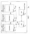
- FIG. Fig. 7 shows a Computer board 800, on which a CPU 802, a working memory (RAM) 804, a first coprocessor 806, a second coprocessor 808 and a third coprocessor 810 arranged are.
- the CPU 802 is connected to the three coprocessors 806, 808, 810 connected via a bus 812.
- a separate memory may be provided which only for coprocessor operations, i. H. a memory 1 814, a memory 2 816 for the coprocessor 2 and a memory 3 818 for the coprocessor 3.
- each chip disposed on the computer board 800 shown in FIG. 7 is supplied with the electric power required for the functioning of the electronic components within the individual elements via its own power supply terminal I 1 to I 8 .
- the board 800 is then distributed via the board to the individual chips on the board.
- the supply lines to the individual chips are available for an attacker.
- each chip on the computer board 800 has a own power or power access, on the without Another of an attacker can be accessed Tapping power profiles or power profiles over time. Capturing performance profiles over time is the foundation faced with a variety of efficient attacks Cryptographic processors. More backgrounds or a detailed Representation of various attacks against cryptography processors are in "Information Leakage Attacks A-gainst Smart Card Implementations of Cryptographic Algorithms and Countermeasures ", Hess et al., Eurosmart Security Conference, June 13 to June 15, 2000, presented. As countermeasures Implementations are proposed which are based on it build up that different operations are always the same Need time, allowing an attacker due to a performance profile can not see if the crypto processor has a Multiplication, an addition, or anything else Has.
- the ZDN method is based on a serial / parallel architecture using parallel executable look-ahead Algorithms for multiplication and modular reduction, by a multiplication of two binary numbers into one iterative 3-operand addition using look-ahead parameters for multiplication and modular reduction to transform.
- This is the modular multiplication decomposed into a serial calculation of partial products.
- two partial products are formed and then taking into account the modular reduction added together to get an intermediate result.
- another partial product is formed and again taking into account the modular reduction to the intermediate result added.
- This iteration continues until all parts of the multiplier have been processed.
- For the three-operand addition involves a crypto-coprocessor an adder, which is in a current iteration step the summation of a new partial product to the intermediate result of the preceding iteration step.
- each coprocessor of FIG. 7 could have its own ZDN unit be equipped to several modular multiplications run parallel to the for certain applications Increase throughput.
- this solution would turn on it fail that an attacker of each chip individually the Can elicit power profiles, so that although an increase in the Throughput has been achieved, but at the expense of security of the cryptography calculator.
- the object of the present invention is to provide a fast and secure cryptography processor.
- the present invention is based on the knowledge that a fast cryptography processor can only be achieved can, if a cryptographic compute operation in several Partial operations is decomposed, and these sub-operations of be executed parallel part calculations. on the other hand can be a security especially against performance monitoring attacks can only be achieved if all sub-calculators including the control unit for the sub-processors and the central processing unit on a single Chip can be arranged so that the power inputs for the individual components not for an external attacker To be available.
- the central processing facility and the coprocessor which has a single control unit as well Has a plurality of sub-calculations, on a single Integrated chip.
- this single chip only has a single supply access to supply the A plurality of sub-processors, the control unit and the central processing unit with power on.
- a limit of parallel processing is then reached if the computational effort in the control unit to distribute the Sub-operations on the sub-processors and for driving the individual part of the calculation increases sharply.
- the multiplication of two very long integers is the ratio of computation time in a partial calculation to the computing time of the control unit so great for organizational and administrative tasks that a considerable degree of parallelism can be achieved without the administrative burden in problematic scales comes.
- Cryptoprocessors are used for safety-critical applications used, for example, for digital signatures, authentications or encryption tasks. An attacker wants For example, find out the secret key to thereby to break the cryptography process.
- Cryptographic processors are used for example in chip cards, which, as has already been stated, smart cards or Signature cards for a legally binding electronic Signature or for home banking or to pay with the mobile phone, etc.
- Typical physical attacks measure power consumption (SPA, DPA, timing attacks) or the electromagnetic radiation.
- SPA power consumption
- DPA timing attacks
- electromagnetic radiation For a more detailed explanation of the attacks reference is made to the references mentioned above.
- an attack typically measures the power consumption of the entire chip card, including the CPU and coprocessor, which is the sum of the individual power consumptions of, for example, the CPU, the RAM, a ROM, an E 2 PROM, a flash memory, a timing controller, a random number generator (RNG), a DES module, and the crypto-coprocessor.
- the CPU and coprocessor which is the sum of the individual power consumptions of, for example, the CPU, the RAM, a ROM, an E 2 PROM, a flash memory, a timing controller, a random number generator (RNG), a DES module, and the crypto-coprocessor.
- the power consumption of an example in CMOS technology manufactured chips changes when switching from one "0" to a "1". Therefore, the power consumption is data dependent as well as the used commands of the CPU and the Cryptocoprocessor.
- Fig. 1 shows a cryptoprocessor according to the invention for Performing operations for cryptographic applications.
- the crypto processor is implemented on a single chip 100 and includes a central processing unit (CPU) 102 and a coprocessor 104.
- the coprocessor 104 is how it is shown in Fig. 1, arranged on the same chip as the central processing unit 102.
- the coprocessor comprises a plurality of partial calculators 106, 108, 110 and 112, wherein each sub-computer 106 to 112 has its own arithmetic Unit AU has.
- each includes Sectionrechen 106 to 112 in addition to the AU at least one Register (REG), as explained with reference to FIG will be able to save intermediate results.
- REG Register
- a typical crypto processor becomes an input interface 114 and an output interface 116, which with external terminals for a data input or a data output and connected to the CPU 102.
- the CPU 102 typically is associated with its own memory 118, which in Fig. 1 is designated RAM.
- the crypto processor another clock generator 120, more memory, random number generators etc., which in Fig. 1 not are shown.
- Fig. 1 Elements are implemented on a single chip, which by a single power supply terminal 122 is supplied with power.
- the chip 100 includes internally Power supply lines to all shown in Fig. 1 Elements, which, however, for reasons given above not can be individually intercepted.
- the power supply connections of each component very much are easily audible, and therefore very "expressive" power profiles that is applied to the power supply terminal 122 Current profile almost constant or indicates a possible homogeneous noise around a constant value. This is due to the fact that the coprocessor 104, which am most contributes to power consumption, a plurality of parallel arranged part of the calculation has independent for example, switch from "0" to "1" and therefore uncorrelated from each other consume electricity.
- the parallel connection of the individual sub-calculators also leads to increase the throughput of the krypton processor can be, so in case of execution of a memory on the chip the consequent loss of speed, which due to different technologies for Memory and arithmetic units occur, more than balanced can be.
- Invention may be two or more sub-computer as so-called Clusters are summarized such that z.
- a first cluster performs partial operations of a first operation
- a second cluster performs partial operations performs second cryptographic operation.
- the first cluster which consists of the partial calculations 106 and 108 exists, for.
- B. two modular exponentiations each with half the length perform, which from a derived from single modular full length exponentiation are, while the second cluster, from the sub-calculations 110 and 112 is a modular multiplication could perform as shown in Fig. 6.
- a cluster could perform an RSA operation, while another cluster performs a DES operation, and another cluster, for example, a hash sum calculated.
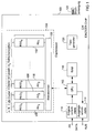
- FIG. 2 shows a more detailed representation of the coprocessor 104 shown in FIG. 1.
- the partial calculation unit 106 comprises, in addition to the arithmetic unit 106 a z. B. three registers 106b, 106c, 106d.
- the sub-computer 108 similarly comprises the arithmetic unit 108a as well as, for example, also three registers 108b, 108c, 108d. The same is true for the partial calculator 112. As shown in FIG.
- the length of the registers of one sub-computer may be different from the length of the register of another sub-computer, so that, for example, with the sub-computer 106, operations with numbers of a length L 1 may be performed while with the sub-computer 102 Operations with numbers of a length L 2 can be performed.
- the control unit 105 may, for example, also actuate the two partial computation units 106 and 108 in such a way that the arithmetic units AU 1 and AU 2 are coupled together in such a way that both partial computation units, which then form a cluster, perform arithmetic operations with numbers of a length L 1 + L 2 carry out.
- the registers of the two sub-processors can thus be interconnected.
- a number of calculation units can also have a number to be assigned exclusively by registers which is so big that the operands for several sub-operations, such.
- the Sub-operations then, for example, by a device for varying the order of the same, in Fig. 2 with 200, superimposed or even mixed at random to further obscure the current profile to reach. This will be especially beneficial if For example, only two partial calculators are available or only two sub-processors work while the others Partial processors of a cryptography processor just stand still.
- control unit 105 further comprises one in FIG. 2 not shown device for switching off partial computation or registers of sub-calculators, if they are not needed, especially for battery-powered applications can be beneficial to the power consumption of the overall circuit to save.
- CMOS devices only need Significant power when switched, but they have also a quiescent current consumption, which then fall into the weight can if the available power is limited is.
- the partial calculations are carried out in such a way that they do such a sub-operation independently without intervention the control unit 105 may perform after the control unit delivered the required command to the calculator Has. Of course every part of the calculation requires this Register for saving the intermediate solutions.
- Control unit 105 Due to the fact that a partial calculation without input of Control unit 105 operates relatively long, the control unit 105 a variety of individual sub-calculations in a sense serial, one after another, with the necessary commands provided in such a way that all sub-processors work in parallel, but in a sense staggered to each other.
- the first part of the calculation becomes one Time activated. Is the control unit 105 with the Activation of the first sub-calculation finished, it performs the same immediately the activation of the second arithmetic unit while the first calculator is already working.
- the third sub-calculation is then activated when activation of the second sub-computer is completed. This means, that while activating the third sub-calculator the first and the second part of the calculation already count. If this is done for all n sub-calculators, so work all partial calculators offset in time. If all part of calculators work in such a way that their sub-operations are the same take a long time, then the first part of the calculation will be finished first be.
- control unit can see the results from the first one Submit the partial calculation unit to the central processing unit and is ideally finished with this transmission, before the second part of the calculation is finished.
- This can be the Throughput can be increased significantly, with an optimal Exploitation of the computing capacity of the control unit 105 achieved becomes. If all sub-operations are identical operations perform, but still creates a heavily veiled Current profile, since all partial calculators are offset in time work. It would be different if all the sub-calculators activated by the control unit at the same time and to work in a completely synchronous way. Then would be a non-obscured power profile and even more reinforced current profile result. Therefore, the serial Activating the partial calculators also with regard to safety the cryptographic processor advantageous.
- Fig. 3 illustrates an apparatus for performing a three-operand addition, as indicated in the formula to the right in Fig. 3.
- the three-operand addition is performed by means of a three-bit adder which operates without a carry, ie a half adder, and a two-bit adder downstream, which works with carry, ie which is a full adder.
- a three-bit adder which operates without a carry, ie a half adder, and a two-bit adder downstream, which works with carry, ie which is a full adder.
- Fig. 3 shows a so-called bit-slice of such adder.
- three numbers with, for example 1024 binary digits would be the arrangement shown in FIG for a fully parallel operation 1024 times in the arithmetic Unit of an arithmetic unit 106 may be present.
- each sub-computer 106 to 112 (FIG. 1) is arranged, to a modular multiplication using the Look-ahead algorithm to execute, in DE 36 31 992 C2 is set forth.
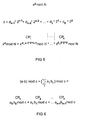
- a required modular multiplication is based on of Fig. 4b explained. It is the task of the binary numbers Multiply "111" and "101" with each other. For this purpose, this multiplication becomes analogous in a partial calculation a multiplication of two numbers according to the known "Schulmathematik" executed, but with binary number representation. Due to the simplicity of illustration will be below the case considered in which no look-ahead algorithm and no modulo reduction is used. If this algorithm is performed, it results first a first partial product "111". This partial product becomes then, to take into account its significance to a position moved to the left. To the first shifted to the left Partial product, as an intermediate result of a first iteration step then, in one second iteration step the second partial product "000" added.
- the multiplicand M represents the partial product if the considered location of the multiplier is a binary "1".
- the partial product is 0 if the considered position of the multiplier is a binary "0".
- the positions or the valences of the partial products are taken into account by the respective displacement operations. In Fig. 4b this is represented by the offset application of the partial products.
- two registers Z 1 and Z 2 are required for the addition of FIG. 4 b. The first partial product could be stored in register Z 1 and then shifted one bit to the left in this register. The second partial product could be stored in register Z 2 . The subtotal could then be stored again in the register Z 1 and then pushed back one bit to the left. The third partial product would be stored again in register Z 2 . The final result would then be in register Z 1 .
- FIG. 4a A schematic flow diagram for the method shown in FIG. 4b can be found in FIG. 4a.
- a step S10 the registers present in a part processor are initialized.
- a step S12 after initialization, a three-operand addition is performed to calculate the first partial product.
- the equation denoted in FIG. S12 would comprise only Z, a 1 and P 1 .
- a 1 can be referred to as the first look-ahead parameter.
- a has a value of "1" if the considered location of the multiplier O is a 1.
- a is equal to zero if the considered digit of the multiplier is a zero.
- step S12 The operation shown in block S12 becomes parallel to all for example, 1024 bits performed. Thereupon will be in a step S14 in the simplest case, a shift operation performed by one position to the right to take into account that the most significant bit of the 2nd partial product one digit lower than the most significant one Bit of the 1st partial product. Have several consecutive Bits of the multiplier O a zero, so finds one Shift by several positions to the right instead. Finally, in a step S16, the parallel again Three-operand addition, for example, using the in Fig. 3 adder chain performed.
- Serial / Parallel means ie the parallel implementation in the block S12 or S16, and serial processing to successively all partial products to combine with each other.
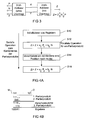
- FIG. 5 The operation x d mod N is considered in FIG. 5.
- the exponent d is represented in binary notation.
- FIG. 5 this results in a chain of modular multiplications, wherein, as also shown in FIG. 5, each modular single operation can each be assigned to a sub-calculator, such that all modular operations are performed in parallel by the one described in FIG 1 cryptography processor shown are executed.
- the intermediate results then obtained, after having been determined in parallel, are multiplied up to obtain the result.
- the control unit 105 controls the division into the individual partial calculation units TRW 1 to TRW k and then the final Aufmultipliring the individual intermediate results.
- FIG. 6 shows another example of a division of an operation (a * b) mod c into a plurality of modular operations.
- the partial calculator TRW 1 can determine a first intermediate result.
- the partial calculators TRW 2 to TRW n also calculate intermediate results, whereupon, after receiving the intermediate results, the control unit 105 controls the multiplication of the intermediate results.
- the control unit controls the summation z. B. so that it selects a partial calculation, which then receives the intermediate results for summation.
- an operation is split into several independent sub-operations.
- FIGS. 5 and 6 serve only to illustrate the possibilities for division an operation in a plurality of sub-operations, wherein quite favorable divisions in terms of achievable Performance can exist.
- Essential to the examples is therefore not the performance of the processor, but that divisions exist, so that each partial calculation one performs independent sub-operation, and that a plurality controlled by sub-operations of a control unit is to create a veiled current profile at the power input to get into the chip.
Landscapes
- Engineering & Computer Science (AREA)
- Theoretical Computer Science (AREA)
- Physics & Mathematics (AREA)
- Software Systems (AREA)
- General Physics & Mathematics (AREA)
- General Engineering & Computer Science (AREA)
- Computer Hardware Design (AREA)
- Mathematical Physics (AREA)
- Computer Security & Cryptography (AREA)
- Pure & Applied Mathematics (AREA)
- Mathematical Optimization (AREA)
- Mathematical Analysis (AREA)
- Computational Mathematics (AREA)
- Computing Systems (AREA)
- Signal Processing (AREA)
- Computer Networks & Wireless Communication (AREA)
- Advance Control (AREA)
- Multi Processors (AREA)
- Storage Device Security (AREA)
- Power Sources (AREA)
- Devices For Executing Special Programs (AREA)
- Bidet-Like Cleaning Device And Other Flush Toilet Accessories (AREA)
- Preparation Of Compounds By Using Micro-Organisms (AREA)
- Microcomputers (AREA)
- Saccharide Compounds (AREA)
Abstract
Description
- Fig. 1
- einen erfindungsgemäßen Kryptoprozessor, der auf einem einzigen Chip integriert ist;
- Fig. 2
- eine detailliertere Darstellung des Coprozessors, welcher verschiedene Teilrechenwerke mit unterschiedlich langen Registern aufweist;
- Fig. 3
- eine detailliertere Darstellung einer Arithmetikeinheit, welche für eine Drei-Operanden-Addition geeignet ist;
- Fig. 4a
- ein schematisches Flussdiagramm zum Durchführen einer modularen Multiplikation auf seriell/parallele Art und Weise;
- Fig. 4b
- ein Zahlenbeispiel zur Veranschaulichung der seriell/parallelen Arbeitsweise einer Arithmetikeinheit am Beispiel einer Multiplikation;
- Fig. 5
- ein Beispiel zum Aufteilen einer modularen Exponentiation in eine Anzahl von modularen Multiplikationen;
- Fig. 6
- ein weiteres Beispiel zum Aufteilen einer modularen Multiplikation auf verschiedene Teilrechenwerke; und
- Fig. 7
- eine Computerplatine mit einer Vielzahl von getrennt versorgten Bauelementen.
Claims (10)
- Kryptographieprozessor zum Durchführen von Operationen für kryptographische Anwendungen, mit folgenden Merkmalen:wobei die Mehrzahl von Teilrechenwerken (106, 108, 110, 112) und die Steuereinheit (105) auf einem einzigen Chip (100) integriert sind, undeiner zentralen Verarbeitungseinheit (102) zum Erhalten von Befehlen für das Ausführen einer Operation und zum Ausgeben von Ergebnissen einer Operation;einem Coprozessor (104), der mit der zentralen Verarbeitungseinheit (102) gekoppelt ist, wobei der Coprozessor folgende Merkmale aufweist:wobei die Steuereinheit (105) ausgebildet ist,eine Mehrzahl von Teilrechenwerken (106, 108, 110, 112), wobei jedes Teilrechenwerk zumindest eine arithmetische Einheit (AU1, AU2, AU3, AUn) aufweist; undeine einzige Steuereinheit (105), die mit jedem der Mehrzahl von Teilrechenwerken gekoppelt ist, und die angeordnet ist, um eine Operation in Teiloperationen aufzuteilen, die Teiloperationen auf die Mehrzahl von Teilrechenwerken zu verteilen, und um die Ausführung der Operation durch die Mehrzahl von Teilrechenwerken zu steuern,
um das die einzelnen Teilrechenwerken seriell mit Befehlen zu versehen,
um ein erstes Teilrechenwerk zu einem bestimmten Zeitpunkt zu aktivieren,
um dann, wenn die Aktivierung des ersten Teilrechenwerks abgeschlossen ist, eine Aktivierung eines zweiten Teilrechenwerks durchzuführen, während das erste Teilrechenwerk bereits arbeitet, so dass die Teilrechenwerke zeitlich versetzt arbeiten,
wobei der Chip (100) einen gemeinsamen Versorgungsstromzugang (122) zum Versorgen der Mehrzahl von Teilrechenwerken und der Steuereinheit mit Strom aufweist. - Kryptographieprozessor nach Patentanspruch 1,
bei dem die Steuereinheit ferner ausgebildet ist, um dann, wenn das erste Teilrechenwerk fertig ist, von dem ersten Teilrechenwerk gelieferte Ergebnisse zu der zentralen Verarbeitungseinheit (102) zu übertragen, während das zweite Teilrechenwerk noch arbeitet. - Kryptographieprozessor nach Patentanspruch 1 oder 2, bei dem die Steuereinheit (105) ausgebildet ist, um die Teilrechenwerke so zu aktivieren, dass alle Teilrechenwerke zeitlich versetzt arbeiten.
- Kryptographieprozessor nach einem der vorhergehenden Patentansprüche, bei dem die Teilrechenwerke ausgebildet sind, dass die ausgeführten Teiloperationen gleich lange dauern.
- Kryptographieprozessor nach Patentanspruch 4,
bei dem die Steuereinheit ferner ausgebildet ist, um dann, wenn das erste Teilrechenwerk fertig ist, von dem ersten Teilrechenwerk gelieferte Ergebnisse zu der zentralen Verarbeitungseinheit (102) zu übertragen, während das zweite Teilrechenwerk noch arbeitet, und
bei dem die Steuereinheit (105) ausgebildet ist, um mit der Übermittlung fertig zu sein, bevor das zweite Teilrechenwerk mit seiner Teiloperation fertig ist. - Kryptographieprozessor nach einem der vorhergehenden Patentansprüche, bei dem sämtliche Teilrechenwerke identische Operationen ausführen.
- Kryptographieprozessor nach einem der vorhergehenden Ansprüche, bei dem jedes Teilrechenwerk ferner eine Mehrzahl von Registern (106b, 106c, 106d, 108b, 108c, 108d) aufweist, die der arithmetischen Einheit (106a, 108a) des jeweiligen Teilrechenwerks exklusiv zugewiesen sind.
- Prozessor nach Anspruch 7,
bei dem sich die Länge (L1, L2) der Mehrzahl von Registern, die einem Teilrechenwerk zugewiesen sind, und der Länge der Mehrzahl von Registern, die einem anderen Teilrechenwerk zugeordnet sind, unterscheiden, derart, dass die Teilrechenwerke arithmetische Berechnung mit jeweils unterschiedlichen langen Zahlen durchführen können. - Kryptographieprozessor nach Anspruch 7 oder Anspruch 8, bei dem die Anzahl der Register, die einem Teilrechenwerk zugeordnet ist, ausreichend ist, um Operanden für zumindest zwei Teiloperationen zu halten, so dass für zumindest zwei Teiloperationen keine Übertragung von Operanden zwischen dem Coprozessor (104) und der zentralen Verarbeitungseinrichtung (102) erforderlich ist.
- Kryptographieprozessor nach Anspruch 9, bei dem die Steuereinheit (105) ferner folgendes Merkmal aufweist:eine Einrichtung (200) zum zeitlichen Steuern des Betriebs der Teilrechenwerke, derart, dass die Reihenfolge der zumindest zwei Teiloperationen, deren Operationen in den Registern eines Teilrechenwerkes gespeichert werden, einstellbar ist.
Applications Claiming Priority (3)
| Application Number | Priority Date | Filing Date | Title |
|---|---|---|---|
| DE10061997 | 2000-12-13 | ||
| DE10061997A DE10061997A1 (de) | 2000-12-13 | 2000-12-13 | Kryptographieprozessor |
| EP01991797.0A EP1342148B9 (de) | 2000-12-13 | 2001-12-06 | Kryptographieprozessor |
Related Parent Applications (3)
| Application Number | Title | Priority Date | Filing Date |
|---|---|---|---|
| EP01991797.0 Division | 2001-12-06 | ||
| EP01991797.0A Division EP1342148B9 (de) | 2000-12-13 | 2001-12-06 | Kryptographieprozessor |
| EP01991797.0A Division-Into EP1342148B9 (de) | 2000-12-13 | 2001-12-06 | Kryptographieprozessor |
Publications (3)
| Publication Number | Publication Date |
|---|---|
| EP1589413A2 true EP1589413A2 (de) | 2005-10-26 |
| EP1589413A3 EP1589413A3 (de) | 2007-04-04 |
| EP1589413B1 EP1589413B1 (de) | 2010-05-05 |
Family
ID=7666917
Family Applications (2)
| Application Number | Title | Priority Date | Filing Date |
|---|---|---|---|
| EP01991797.0A Expired - Lifetime EP1342148B9 (de) | 2000-12-13 | 2001-12-06 | Kryptographieprozessor |
| EP05012165A Expired - Lifetime EP1589413B1 (de) | 2000-12-13 | 2001-12-06 | Kryptographieprozessor |
Family Applications Before (1)
| Application Number | Title | Priority Date | Filing Date |
|---|---|---|---|
| EP01991797.0A Expired - Lifetime EP1342148B9 (de) | 2000-12-13 | 2001-12-06 | Kryptographieprozessor |
Country Status (8)
| Country | Link |
|---|---|
| US (2) | US7430293B2 (de) |
| EP (2) | EP1342148B9 (de) |
| KR (1) | KR20030062422A (de) |
| CN (1) | CN1273876C (de) |
| AT (1) | ATE467172T1 (de) |
| AU (1) | AU2002231668A1 (de) |
| DE (2) | DE10061997A1 (de) |
| WO (1) | WO2002048845A2 (de) |
Families Citing this family (35)
| Publication number | Priority date | Publication date | Assignee | Title |
|---|---|---|---|---|
| DE10253285B4 (de) * | 2002-11-15 | 2018-11-15 | Giesecke+Devrient Mobile Security Gmbh | Verschleierung eines geheimen Wertes |
| US20040230813A1 (en) * | 2003-05-12 | 2004-11-18 | International Business Machines Corporation | Cryptographic coprocessor on a general purpose microprocessor |
| KR100680025B1 (ko) * | 2005-07-05 | 2007-02-07 | 한국전자통신연구원 | 멀티세션 고속암복호화 처리 장치 및 방법 |
| US7916864B2 (en) * | 2006-02-08 | 2011-03-29 | Nvidia Corporation | Graphics processing unit used for cryptographic processing |
| CN100369074C (zh) * | 2006-03-02 | 2008-02-13 | 西安西电捷通无线网络通信有限公司 | 一种实现sms4密码算法中加解密处理的方法 |
| US7826612B2 (en) * | 2006-06-29 | 2010-11-02 | Intel Corporation | System, method and apparatus for an incremental modular process including modular multiplication and modular eduction |
| DE102007007699A1 (de) * | 2007-02-09 | 2008-08-14 | IHP GmbH - Innovations for High Performance Microelectronics/Institut für innovative Mikroelektronik | Reduktion von Seiten-Kanal-Informationen durch interagierende Krypto-Blocks |
| EP2000936A1 (de) | 2007-05-29 | 2008-12-10 | Gemplus | Elektronisches Token mit mehreren Mikroprozessoren und Verfahren zur Verwaltung der Befehlsausführung auf mehreren Mikroprozessoren |
| US8781111B2 (en) * | 2007-07-05 | 2014-07-15 | Broadcom Corporation | System and methods for side-channel attack prevention |
| US7929707B1 (en) * | 2007-09-06 | 2011-04-19 | Elcomsoft Co. Ltd. | Use of graphics processors as parallel math co-processors for password recovery |
| US8670557B2 (en) * | 2007-09-10 | 2014-03-11 | Spansion Llc | Cryptographic system with modular randomization of exponentiation |
| US8139763B2 (en) * | 2007-10-10 | 2012-03-20 | Spansion Llc | Randomized RSA-based cryptographic exponentiation resistant to side channel and fault attacks |
| IL187043A0 (en) * | 2007-10-30 | 2008-02-09 | Sandisk Il Ltd | Secure pipeline manager |
| US20090183161A1 (en) * | 2008-01-16 | 2009-07-16 | Pasi Kolinummi | Co-processor for stream data processing |
| JP5146156B2 (ja) * | 2008-06-30 | 2013-02-20 | 富士通株式会社 | 演算処理装置 |
| ITMI20082364A1 (it) | 2008-12-31 | 2010-07-01 | Incard Sa | Metodo per proteggere un dispositivo crittografico contro attacchi spa, dpa e temporali |
| US20100177889A1 (en) * | 2009-01-15 | 2010-07-15 | Kabushiki Kaisha Toshiba | Image forming apparatus and encryption process control method |
| US20100306553A1 (en) * | 2009-06-01 | 2010-12-02 | Poletti Iii Joseph William | High-throughput cryptographic processing using parallel processing |
| EP2293185A1 (de) * | 2009-09-04 | 2011-03-09 | Thomson Licensing | Gegen Übersprungangriffe gesichertes Exponentiationsverfahren und Vorrichtung zum Durchführen des Verfahrens |
| US20140032917A1 (en) * | 2010-10-29 | 2014-01-30 | Nec Corporation | Group signature processing device for processing a plurality of group signatures simultaneously |
| DE102011007976A1 (de) | 2011-01-03 | 2012-07-05 | Giesecke & Devrient Gmbh | Verfahren zur gesicherten Ausführung einer Kryptographischen Berechnung |
| JP5776927B2 (ja) * | 2011-03-28 | 2015-09-09 | ソニー株式会社 | 情報処理装置及び方法、並びにプログラム |
| EP2523385B1 (de) * | 2011-05-05 | 2017-07-12 | Proton World International N.V. | Verfahren und Schaltung für kryptografische Operation |
| WO2012159191A1 (en) | 2011-05-20 | 2012-11-29 | Research In Motion Limited | Verifying passwords on a mobile device |
| US8958550B2 (en) * | 2011-09-13 | 2015-02-17 | Combined Conditional Access Development & Support. LLC (CCAD) | Encryption operation with real data rounds, dummy data rounds, and delay periods |
| WO2014028005A1 (en) * | 2012-08-14 | 2014-02-20 | Empire Technology Development Llc | Software-based side-channel attack prevention |
| EP2733654A1 (de) * | 2012-11-20 | 2014-05-21 | Nagravision S.A. | Elektronisches Bezahlverfahren, System und Vorrichtung zum sicheren Austausch von Bezahlinformationen |
| US9419993B2 (en) * | 2013-12-12 | 2016-08-16 | Empire Technology Development Llc | Randomization of processor subunit timing to enhance security |
| WO2015096167A1 (en) | 2013-12-28 | 2015-07-02 | Intel Corporation | Rsa algorithm acceleration processors, methods, systems, and instructions |
| EP3152859A1 (de) | 2014-06-04 | 2017-04-12 | Giesecke & Devrient GmbH | Verfahren für erhöhte sicherheit von computervorrichtung mit mehreren kernen |
| US9798521B2 (en) * | 2014-08-27 | 2017-10-24 | Schlage Lock Company Llc | System, method and apparatus for random number generation |
| EP3279826A1 (de) * | 2016-08-04 | 2018-02-07 | Nagravision SA | Sequenzverifikation |
| CN107294719A (zh) * | 2017-06-19 | 2017-10-24 | 北京万协通信息技术有限公司 | 一种双线性对运算的加解密协处理器 |
| FR3076925B1 (fr) | 2018-01-16 | 2020-01-24 | Proton World International N.V. | Fonction cryptographique |
| EP4351078B1 (de) * | 2021-06-22 | 2025-08-06 | Huawei Technologies Co., Ltd. | Datenverarbeitungsverfahren und prozessor |
Family Cites Families (10)
| Publication number | Priority date | Publication date | Assignee | Title |
|---|---|---|---|---|
| GB2130405B (en) | 1980-08-30 | 1984-11-21 | British Aerospace | Electronic calculator |
| DE3631992A1 (de) * | 1986-03-05 | 1987-11-05 | Holger Sedlak | Kryptographie-verfahren und kryptographie-prozessor zur durchfuehrung des verfahrens |
| ATE55033T1 (de) | 1986-03-05 | 1990-08-15 | Holger Sedlak | Kryptographie-verfahren und kryptographieprozessor zur durchfuehrung des verfahrens. |
| US5752071A (en) * | 1995-07-17 | 1998-05-12 | Intel Corporation | Function coprocessor |
| DE19539700C1 (de) * | 1995-10-25 | 1996-11-28 | Siemens Ag | Sicherheitschip |
| GB9707861D0 (en) * | 1997-04-18 | 1997-06-04 | Certicom Corp | Arithmetic processor |
| US6219420B1 (en) * | 1998-09-02 | 2001-04-17 | Motorola, Inc. | High assurance encryption system and method |
| US6408075B1 (en) * | 1998-11-30 | 2002-06-18 | Hitachi, Ltd. | Information processing equipment and IC card |
| FR2787900B1 (fr) * | 1998-12-28 | 2001-02-09 | Bull Cp8 | Circuit integre intelligent |
| FR2789535B1 (fr) * | 1999-02-04 | 2001-09-28 | Bull Cp8 | Procede de securisation d'un ensemble electronique de cryptographie a cle secrete contre les attaques par analyse physique |
-
2000
- 2000-12-13 DE DE10061997A patent/DE10061997A1/de not_active Withdrawn
-
2001
- 2001-12-06 WO PCT/EP2001/014349 patent/WO2002048845A2/de not_active Ceased
- 2001-12-06 AU AU2002231668A patent/AU2002231668A1/en not_active Abandoned
- 2001-12-06 AT AT05012165T patent/ATE467172T1/de not_active IP Right Cessation
- 2001-12-06 EP EP01991797.0A patent/EP1342148B9/de not_active Expired - Lifetime
- 2001-12-06 CN CNB018205658A patent/CN1273876C/zh not_active Expired - Fee Related
- 2001-12-06 EP EP05012165A patent/EP1589413B1/de not_active Expired - Lifetime
- 2001-12-06 DE DE50115478T patent/DE50115478D1/de not_active Expired - Lifetime
- 2001-12-06 KR KR10-2003-7007883A patent/KR20030062422A/ko not_active Abandoned
-
2003
- 2003-06-13 US US10/461,905 patent/US7430293B2/en not_active Expired - Fee Related
-
2008
- 2008-02-20 US US12/034,252 patent/US8369520B2/en not_active Expired - Fee Related
Also Published As
| Publication number | Publication date |
|---|---|
| CN1273876C (zh) | 2006-09-06 |
| ATE467172T1 (de) | 2010-05-15 |
| CN1481524A (zh) | 2004-03-10 |
| EP1342148B1 (de) | 2013-07-03 |
| EP1589413B1 (de) | 2010-05-05 |
| DE10061997A1 (de) | 2002-07-18 |
| KR20030062422A (ko) | 2003-07-25 |
| EP1342148A2 (de) | 2003-09-10 |
| WO2002048845A2 (de) | 2002-06-20 |
| US7430293B2 (en) | 2008-09-30 |
| WO2002048845A3 (de) | 2002-11-14 |
| AU2002231668A1 (en) | 2002-06-24 |
| US20080140739A1 (en) | 2008-06-12 |
| EP1589413A3 (de) | 2007-04-04 |
| US8369520B2 (en) | 2013-02-05 |
| US20040105541A1 (en) | 2004-06-03 |
| EP1342148B9 (de) | 2014-02-26 |
| DE50115478D1 (de) | 2010-06-17 |
Similar Documents
| Publication | Publication Date | Title |
|---|---|---|
| EP1589413B1 (de) | Kryptographieprozessor | |
| EP1342154B1 (de) | Kryptographieprozessor | |
| DE10136335B4 (de) | Prozessor mit mehreren Rechenwerken | |
| EP1859344A2 (de) | Verfahren und vorrichtung zum berechnen einer polynom-multiplikation, insbesondere für die elliptische kurven-kryptographie | |
| EP1395910B1 (de) | Elektronische schaltung mit asynchroner taktung von peripherieeinheiten | |
| EP1324188A2 (de) | Verfahren zum Multiplizieren zweier Faktoren aus dem Galois-Feld sowie Multiplizierer zum Durchführen des Verfahrens | |
| DE69700018T2 (de) | Koprozessor für moduläre Arithmetik mit einer schnellen Ausführung von nicht-modulären Operationen | |
| DE10219158A1 (de) | Vorrichtung und Verfahren zum Berechnen eines Ergebnisses einer modularen Multiplikation | |
| EP1046142B1 (de) | Datenverarbeitungseinrichtung und verfahren zu dessen betrieb zum verhindern einer differentiellen stromverbrauchanalyse | |
| DE10224742B4 (de) | Datenverarbeitungsschaltung und Verfahren zum Übertragen von Daten | |
| EP1080400B1 (de) | Verfahren und vorrichtung zum verarbeiten von daten | |
| EP1506473B1 (de) | Ausspähungsgeschützte modulare inversion | |
| DE60220793T2 (de) | Verwürfelung bzw. Verschleierung (Scrambling) einer Berechnung, bei welcher eine modulare Funktion zur Anwendung kommt | |
| DE102022129607A1 (de) | Schaltung für kombinierten schlüsselwertabhängigen austausch und randomisierung von zwei werten | |
| DE10219164B4 (de) | Vorrichtung und Verfahren zum Berechnen eines ganzzahligen Quotienten | |
| DE10156708B4 (de) | Verfahren und Vorrichtung zum Multiplizieren und Verfahren und Vorrichtung zum Addieren auf einer elliptischen Kurve | |
| DE102022130488A1 (de) | Verarbeitungsschaltung | |
| DE10129241B4 (de) | Multifunktionaler Rechner | |
| DE10225230B4 (de) | Prozessor und Verfahren zum gleichzeitigen Ausführen einer Berechnung und eines Kopiervorgangs | |
| DE19960047A1 (de) | Verfahren und Einheit zur sicheren Informationsbehandlung in einem kryptographischen Informationsverarbeitungssystem | |
| DE102022129606A1 (de) | Schaltung für kombinierten schlüsselwertabhängigen austausch und multiplikative randomisierung von zwei werten | |
| DE10108916C1 (de) | Schaltung zum wahlweisen Teilen, Teilerschaltung und Verfahren zum Teilen einer Zahl | |
| DE10221409A1 (de) | Schaltung und Verfahren zur Durchführung einer Berechnung | |
| DE10215771A1 (de) | Konfigurierbares Rechenwerk |
Legal Events
| Date | Code | Title | Description |
|---|---|---|---|
| PUAI | Public reference made under article 153(3) epc to a published international application that has entered the european phase |
Free format text: ORIGINAL CODE: 0009012 |
|
| 17P | Request for examination filed |
Effective date: 20050606 |
|
| AC | Divisional application: reference to earlier application |
Ref document number: 1342148 Country of ref document: EP Kind code of ref document: P |
|
| AK | Designated contracting states |
Kind code of ref document: A2 Designated state(s): AT DE ES FR GB IT |
|
| PUAL | Search report despatched |
Free format text: ORIGINAL CODE: 0009013 |
|
| AK | Designated contracting states |
Kind code of ref document: A3 Designated state(s): AT DE ES FR GB IT |
|
| RIC1 | Information provided on ipc code assigned before grant |
Ipc: G06F 21/00 20060101ALI20070226BHEP Ipc: G06F 7/72 20060101ALI20070226BHEP Ipc: G06F 9/38 20060101AFI20050902BHEP |
|
| AKX | Designation fees paid |
Designated state(s): AT DE ES FR GB IT |
|
| 17Q | First examination report despatched |
Effective date: 20080925 |
|
| GRAP | Despatch of communication of intention to grant a patent |
Free format text: ORIGINAL CODE: EPIDOSNIGR1 |
|
| GRAS | Grant fee paid |
Free format text: ORIGINAL CODE: EPIDOSNIGR3 |
|
| GRAA | (expected) grant |
Free format text: ORIGINAL CODE: 0009210 |
|
| AC | Divisional application: reference to earlier application |
Ref document number: 1342148 Country of ref document: EP Kind code of ref document: P |
|
| AK | Designated contracting states |
Kind code of ref document: B1 Designated state(s): AT DE ES FR GB IT |
|
| REG | Reference to a national code |
Ref country code: GB Ref legal event code: FG4D Free format text: NOT ENGLISH |
|
| RAP2 | Party data changed (patent owner data changed or rights of a patent transferred) |
Owner name: INFINEON TECHNOLOGIES AG |
|
| REF | Corresponds to: |
Ref document number: 50115478 Country of ref document: DE Date of ref document: 20100617 Kind code of ref document: P |
|
| PG25 | Lapsed in a contracting state [announced via postgrant information from national office to epo] |
Ref country code: ES Free format text: LAPSE BECAUSE OF FAILURE TO SUBMIT A TRANSLATION OF THE DESCRIPTION OR TO PAY THE FEE WITHIN THE PRESCRIBED TIME-LIMIT Effective date: 20100816 |
|
| REG | Reference to a national code |
Ref country code: FR Ref legal event code: CA |
|
| PLBE | No opposition filed within time limit |
Free format text: ORIGINAL CODE: 0009261 |
|
| STAA | Information on the status of an ep patent application or granted ep patent |
Free format text: STATUS: NO OPPOSITION FILED WITHIN TIME LIMIT |
|
| PG25 | Lapsed in a contracting state [announced via postgrant information from national office to epo] |
Ref country code: IT Free format text: LAPSE BECAUSE OF FAILURE TO SUBMIT A TRANSLATION OF THE DESCRIPTION OR TO PAY THE FEE WITHIN THE PRESCRIBED TIME-LIMIT Effective date: 20100505 |
|
| 26N | No opposition filed |
Effective date: 20110208 |
|
| REG | Reference to a national code |
Ref country code: DE Ref legal event code: R097 Ref document number: 50115478 Country of ref document: DE Effective date: 20110207 |
|
| PG25 | Lapsed in a contracting state [announced via postgrant information from national office to epo] |
Ref country code: AT Free format text: LAPSE BECAUSE OF NON-PAYMENT OF DUE FEES Effective date: 20101206 |
|
| REG | Reference to a national code |
Ref country code: AT Ref legal event code: MM01 Ref document number: 467172 Country of ref document: AT Kind code of ref document: T Effective date: 20101206 |
|
| REG | Reference to a national code |
Ref country code: FR Ref legal event code: PLFP Year of fee payment: 15 |
|
| REG | Reference to a national code |
Ref country code: FR Ref legal event code: PLFP Year of fee payment: 16 |
|
| PGFP | Annual fee paid to national office [announced via postgrant information from national office to epo] |
Ref country code: DE Payment date: 20170214 Year of fee payment: 16 |
|
| REG | Reference to a national code |
Ref country code: FR Ref legal event code: PLFP Year of fee payment: 17 |
|
| PGFP | Annual fee paid to national office [announced via postgrant information from national office to epo] |
Ref country code: FR Payment date: 20171221 Year of fee payment: 17 |
|
| PGFP | Annual fee paid to national office [announced via postgrant information from national office to epo] |
Ref country code: GB Payment date: 20171221 Year of fee payment: 17 |
|
| REG | Reference to a national code |
Ref country code: DE Ref legal event code: R119 Ref document number: 50115478 Country of ref document: DE |
|
| PG25 | Lapsed in a contracting state [announced via postgrant information from national office to epo] |
Ref country code: DE Free format text: LAPSE BECAUSE OF NON-PAYMENT OF DUE FEES Effective date: 20180703 |
|
| GBPC | Gb: european patent ceased through non-payment of renewal fee |
Effective date: 20181206 |
|
| PG25 | Lapsed in a contracting state [announced via postgrant information from national office to epo] |
Ref country code: FR Free format text: LAPSE BECAUSE OF NON-PAYMENT OF DUE FEES Effective date: 20181231 |
|
| PG25 | Lapsed in a contracting state [announced via postgrant information from national office to epo] |
Ref country code: GB Free format text: LAPSE BECAUSE OF NON-PAYMENT OF DUE FEES Effective date: 20181206 |