EP2523385B1 - Verfahren und Schaltung für kryptografische Operation - Google Patents
Verfahren und Schaltung für kryptografische Operation Download PDFInfo
- Publication number
- EP2523385B1 EP2523385B1 EP11164951.3A EP11164951A EP2523385B1 EP 2523385 B1 EP2523385 B1 EP 2523385B1 EP 11164951 A EP11164951 A EP 11164951A EP 2523385 B1 EP2523385 B1 EP 2523385B1
- Authority
- EP
- European Patent Office
- Prior art keywords
- binary
- cryptographic
- digit
- bits
- base
- Prior art date
- Legal status (The legal status is an assumption and is not a legal conclusion. Google has not performed a legal analysis and makes no representation as to the accuracy of the status listed.)
- Active
Links
Images
Classifications
-
- H—ELECTRICITY
- H04—ELECTRIC COMMUNICATION TECHNIQUE
- H04L—TRANSMISSION OF DIGITAL INFORMATION, e.g. TELEGRAPHIC COMMUNICATION
- H04L9/00—Cryptographic mechanisms or cryptographic arrangements for secret or secure communications; Network security protocols
- H04L9/002—Countermeasures against attacks on cryptographic mechanisms
- H04L9/004—Countermeasures against attacks on cryptographic mechanisms for fault attacks
-
- H—ELECTRICITY
- H04—ELECTRIC COMMUNICATION TECHNIQUE
- H04L—TRANSMISSION OF DIGITAL INFORMATION, e.g. TELEGRAPHIC COMMUNICATION
- H04L9/00—Cryptographic mechanisms or cryptographic arrangements for secret or secure communications; Network security protocols
- H04L9/06—Cryptographic mechanisms or cryptographic arrangements for secret or secure communications; Network security protocols the encryption apparatus using shift registers or memories for block-wise or stream coding, e.g. DES systems or RC4; Hash functions; Pseudorandom sequence generators
-
- H—ELECTRICITY
- H04—ELECTRIC COMMUNICATION TECHNIQUE
- H04L—TRANSMISSION OF DIGITAL INFORMATION, e.g. TELEGRAPHIC COMMUNICATION
- H04L2209/00—Additional information or applications relating to cryptographic mechanisms or cryptographic arrangements for secret or secure communication H04L9/00
- H04L2209/12—Details relating to cryptographic hardware or logic circuitry
Definitions
- the present invention relates to a method and circuit for performing a cryptographic operation, and in particular to a method and circuit for performing a hardware implemented cryptographic operation.
- a cryptographic access device such as an IC (integrated circuit) card or the like
- a cryptographic access device such as an IC (integrated circuit) card or the like
- the cryptographic operations performed by such access devices are generally implemented in dedicated hardware, rather than in software, which provides some protection against cloning by making it harder to recover the secret key from the chip.
- fraudsters may still be able to emulate the cryptographic operations in software executable by a general purpose processor.
- a fraudster may obtain information regarding the encryption key stored on the card using side channel attacks such as DPA (differential power analysis) and/or fault injection involving sweeping the surface of the chip using a laser beam to change one or more bit values.
- side channel attacks such as DPA (differential power analysis) and/or fault injection involving sweeping the surface of the chip using a laser beam to change one or more bit values.
- a method of slowing the execution time of a software implementation of a cryptographic operation with respect to its hardware implementation comprising performing a cryptographic operation comprising: receiving a plurality of binary input values; performing a transformation on the binary input values to form a plurality of non-binary digits of base r, where r is an integer greater than 2 and not equal to a power of 2, the transformation involving splitting said binary input values into tuples of bits, the number of bits z forming each tuple being chosen such that 2 Z is smaller than r, each non-binary digit being represented by a plurality of bits, wherein not all possible binary combinations are used; and performing, by a cryptographic block a different modulo r operation on each digit of the plurality of non-binary digits, to generate at least one output digit of base r.
- the method further comprises extracting from said at least one output digit of base r a plurality of binary output values.
- each operation of base r comprises a modular addition, subtraction and/or multiplication of said non-binary digit with at least one further non-binary digit, and/or taking the modular additive or multiplicative inverse.
- r is a prime number not equal to 2.
- r is equal to 2 n -1, where n is an integer equal to or greater than 2.
- the method further comprises generating an alert signal if the execution time of said cryptographic operation exceeds a set time limit.
- said cryptographic operation comprises one of: a sponge function; a stream cipher; a compression function of a hash function; an iterated permutation; a block cipher; and a message authentication operation.
- the method further comprises generating an alert if said plurality of digits has a combination that does not represent a digit of base r.
- a circuit for performing a cryptographic operation for which the execution time of a software implementation of the cryptographic operation is slowed with respect to its hardware implementation, the circuit comprising: a first block adapted to perform a transformation on the binary input values to form a plurality of non-binary digits of base r, where r is an integer greater than 2 and not equal to a power of 2, the transformation involving splitting a plurality of binary input data values into tuples of bits and the number of bits z forming each tuple being chosen such that 2 Z is smaller than r, each non-binary digit being represented by a plurality of bits, wherein not all possible binary combinations are used; and a cryptographic block adapted to perform on each of the plurality of non-binary digits, a different modulo r operation to generate at least one output digit of base r.
- the circuit further comprises: a second block adapted to extract, from said at least one output digit of base r, a plurality of binary output values.
- an IC card comprising the above circuit.
- a cryptographic access system comprising the above circuit; and a receptor device adapted to communicate with said circuit.
- said receptor device comprises a verification block adapted to generate an alert if the execution time of said cryptographic operation exceeds a time limit.
- said receptor is at least one of: a set-top box; a device adapted to permit a user to physically access to a restricted area; a device adapted to permit a user to access a restricted area of an internet site.
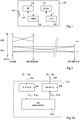
- Figure 1 illustrates a cryptographic access device 100, which is for example a smart card, or other type of integrated circuit card comprising a chip that implements a cryptographic operation.
- the device 100 comprises an input/output port (I/O) 102, which for example contains a suitable interface for communicating with a receptor device (not shown in Figure 1 ), which could for example be a set-top box, or other terminal capable of communications with the device 100.
- I/O input/output port
- the input/output port 102 is coupled to a bus 104 of the device 100, via which access is provided to a processing unit (PU) 106, a memory (MEM) 108, and an algorithm block (ALGO) 110, which implements a cryptographic algorithm in hardware.
- the cryptographic algorithm may make use of a cryptographic key, which should remain secret, and is for example stored in a protected memory on chip.
- the bus 104 is also coupled to a function block 112, which for example implements other functions of the device 100 depending on the particular application.
- Figure 2 shows timing diagrams illustrating an example of the runtimes of the hardware implementation of the cryptographic algorithm of block 110 of Figure 1 , and of its software emulation.
- the cryptographic algorithm is to be performed on data received at the input/output port 102 at a time t 0 , and that the algorithm starts processing this data a short time later, at a time t 1 .
- the result of the cryptographic operation is made available by the hardware implementation. For example, the delay between t 1 and t 2 is in the region of a few tens of milliseconds.
- the software emulation of the cryptographic function also starts processing the input data at time t 1 .
- the result of the software emulation is available at a time t 3 , which is a significant time delay after the time t 2 .
- the delay between t 1 and t 3 is at least ten times the delay between t 1 and t 2 , or even as high as fifty times or greater, and could be in the region of hundreds of milliseconds or a few seconds.
- the cryptographic algorithm is designed in such a way that its implementation in software is far less efficient than the hardware implementation. This is achieved at least in part by the use of a cryptographic primitive that operates on a state consisting of non-binary digits rather than bytes or bit-strings.
- non-binary digit is used to denote any symbol that has a range of r values that is not a power of two. For example, symbols in the range [0...6] have 7 possible values, and will be referred to herein as digits of base 7.
- An operation performed to the base r will be referred to herein as a "modulo r" or "(mod r)" calculation. Examples of such modulo r operations include modular addition, taking the additive modular inverse, modular multiplication and taking the modular multiplicative inverse.
- the cryptographic primitive for example comprises a non-uniform operation performed on the non-binary digits, such as a non-uniform arithmetic operation.
- non-uniform is used herein to designate an operation in which each digit of a state is treated differently, for example by functions that are qualitatively different from each other.
- the values of digits of the state are updated based on the old values according to a modular arithmetic function that differs qualitatively from digit to digit.
- a different modulo r function is applied to each digit, one function for example being a modulo r addition, another being a modulo r multiplication, etc.
- the increased time delay of the software emulation can render, in certain applications, the use of the software emulation impossible.
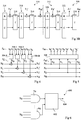
- FIG 3A schematically illustrates an embodiment of the hardware of the algorithm block 110 of Figure 1 in more detail.
- the cryptographic operation implemented by block 110 is for example any cryptographic primitive that does not use the implementation of an inverse mapping for its operation.
- the operation comprises stream ciphers, hash functions, in particular compression functions of a hash function, and/or block ciphers, used in modes that do not use the inverse cipher.
- the modes of the operation could be the output feedback mode, counter mode, or modes used for message authentication (MAC).
- MAC message authentication
- the operation could also comprise an iterated permutation or the sponge function.
- Block 110 comprises an input 302 comprising one or more lines for receiving, in parallel or in serial, input data values P 0 to P N , which could represent: plaintext prior to being subject to a MAC computation, hash computation or authenticated encryption; encrypted data and data to be authenticated; one or more cryptographic keys; or other data for use during a cryptographic operation.
- Each input data value P 0 to P N for example comprises a single bit or a plurality of bits, such as a word of 8, 16 or 32 bits.
- the cryptographic operations to be performed by algorithm block 110 are based on a state consisting of an array of non-binary digits. This for example involves injecting the input data and/or a key into the state of the cryptographic primitive.
- a transformation of the input data is first performed, which involves splitting the binary data bits into groups of bits, referred to herein as tuples of bits. Each tuple of bits is interpreted as an integer. The number of bits z forming each tuple is chosen such that 2 Z is smaller than the number of possible values of the digit, in other words it is smaller than the base r.
- the input data values P 0 to P N are provided to a binary to non-binary block (B TO NB) 304, which provides M+1 data digits P 0 ' to P M ', by splitting the data values P 0 ' to P N ' into tuples of bits.
- B TO NB binary to non-binary block
- the base r of the data values P 0 ' to P M ' is an integer greater than 2 and not equal to a power of 2.
- r is an odd integer greater than 1.
- r is a prime number greater than 2.
- this redundancy can be minimized by choosing r equal to 2 n -1, for integer values of n greater than 1.
- r is equal to 3, 7 or 15.
- the base-r digits P 0 ' to P M ' are provided to a base-r cryptographic block (CRYPTO BLOCK) 306, which performs a non-binary operation on each of the digits.
- block 306 for example performs a sequence of operations, such as additions, subtractions and/or multiplications, modulo the base r.
- the operation comprises a number of iterations of a round function consisting of nonlinear operations such as modular multiplications among the state digits, mixing operations, i.e. modular additions among neighboring state digits, and transpositions, i.e. moving the state digits around.
- block 306 for example comprises table lookups.
- the block for example comprises a base-r cryptographic primitive or module, into which data and/or keys are injected, and from which blocks of bits are extracted.
- Each of the binary digits is for example applied to a corresponding state value, for example by addition or multiplication, and thus each digit is treated in a different way, leading to a non-uniform implementation.
- the output of the cryptographic block 306 is provided in the form of base-r digits Z 0 ' to Z M ', which are provided to a binary extraction block (NB to B) 308, which extracts binary values from the non-binary base-r digits, to generate output binary data values Z 0 to Z N on one or more lines 309.
- block 308 extracts a block of N blocks of bits from M base-r digits.
- the use of the output bits will depend on the particular application. For example, in the case of data encryption, the input values P 0 to P N for example correspond to the encryption key, and output values Z 0 to Z N are added to a plaintext data stream.
- protection against fault attacks may be provided based on the use of base-r digits, where r is not equal to a power of 2.
- each non-binary digit is for example represented by a plurality of bits.
- the bits "00" represent the value 0
- the bits "01” represent the value 1
- the bits "10” represent the value 2.
- the bit combination "11" would never occur, and thus the occurrence of this combination would indicate the presence of a fault.
- Figure 3B schematically represents the operation of the non-binary operation block 306 of Figure 3A according to one particular example in which the operation is a sponge function, comprising an absorbing portion 310, and a squeezing portion 312.
- Sponge functions are for example described in more detail in the publication entitled "Sponge functions", by G. Bertoni et al.
- An initial state 314 comprises R digits forming a first group and C digits forming a second group.
- An iterative operation is then performed, in which a first of the data values P 0 ' is added to the R digits of the initial state 314, and the resulting value, along with the C digits of the initial state, are provided to a function block 316.
- the function block 316 performs a function on the data values, for example a permutation among the groups of R and C digits, including at least one permutation between the groups.
- the output of the function block 316 provides a new state 318, having groups of modified R and C digits.
- the final state resulting from the absorbing phase 310 forms the initial state 320.
- the R digits of this initial state 320 are extracted as a first output data value Z 0 '.
- the R and C groups of digits are provided to the function block 316, which performs the same function on these digits as during the absorbing phase. This process is iteratively repeated to extract the next data value Z 1 ', and then again until the final output data value Z M ' has been extracted after M+1 iterations.
- Figure 4 illustrates an example implementation of the binary to non-binary conversion and the addition of the non-binary digits of the digits P 0 ' to P M ' to the R digits of the state.
- each data value P n for integer values of n between 0 and N, consists of binary bits b 0 to b k . Furthermore, it is assumed in the example of Figure 4 that the base is 7, in other words that each digit is in base 7.
- the bits b 0 to b k are split into pairs by corresponding sub-blocks 304-0 to 304-R of the block 304, to provide corresponding digits Y 0 to Y R of the digits P 0 ' to P M ' in base 7.
- the digits Y 0 to Y R each have a number value of 0, 1, 2 or 3, and each is represented by three bits.
- Each of these values Y 0 to Y R is added, modulo 7, to a corresponding digit X 0 to X R of the state, also represented by three bits, to provide the modified digits X 0 ' to X R ' of base 7, which are provided to the function block 316.
- the number R of digits is for example equal to half the number k+1 of input bits.
- FIG. 5 illustrates the extraction, from the R digits of a current state, of a binary data value Z m , for integer values of m between 0 and M.
- each of the digits X 0 to X R of the current state is provided to the extraction block 308.
- Each digit X 0 to X R is for example represented by three bits, and block 308 perform a logic operation on these bits to generate the binary values b 0 ' to b k ' of the output data value Z m .
- the techniques also used for generating error detecting codes can be used to reduce this imbalance.
- the number of output bits is much lower than the number of input bits, and for example the sum (mod 2) of any combination of output bits is equal to the sum (mod 2) of at least z input bits, where z is greater than 2 and for example equal to 10 or more.
- the imbalance of the input bits is x
- the imbalance of the output bits is x Z .
- the non-binary digits are represented by the equivalent number in binary.
- the digit 6 in base 7 is represented by three bits "110". This need not be the case, as the choice of the particular bit combination representing each non-binary digit is arbitrary. However, whatever the representation, there will be some redundancy, as not all of the possible binary combinations will be used. The remaining combinations of the binary bits can be used to provide additional protection of the circuit against fault injection, as will now be described with reference to Figure 6 .
- Figure 6 illustrates verification circuitry 600 comprising AND gates A 0 to A R , which respectively receive the bits representing each digit X 0 to X R .
- the digits are of base 7, each represented by three bits, and the value "111", which would represent the integer 7, is not used.
- block 602 receives the output of each of the AND gates A 0 to A R , and generates an alert on a line 604 signaling the occurrence of a fault in one or more of the digits if the output of any of the AND gates goes high.
- block 602 could simply be an OR gate, that outputs a "1" if there is at least one fault.
- the block 602 comprises a counter, which triggers the alert on line 604 after a certain number of faults have been detected.
- the alert on line 604 for example resets the chip, or renders the chip temporally or permanently disabled.
- the verification circuit 600 could for example be provided to test the digits of the current state of Figure 3B before or after each operation implemented by the function block 306.
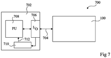
- Figure 7 illustrates a cryptographic access system 700, comprising a receptor 702 that communicates, via an interface 704, with the cryptographic access device 100 of Figure 1 described above.
- the interface between the receptor device 702 and the access device 100 may be any one of various interface types, such as a physical contact between connection pads on the device 100 with pins of the receptor device 702 (pads and pins not shown in Figure 7 ), or by a wireless interface, such as by RF communication.
- the receptor device 702 is for example a set-top box, such as a satellite, ADSL, or cable television decoder, a device adapted to permit a user to physically access to a restricted area, such as an entry gate system, or ticket gate of a travel network, a device adapted to permit a user to access a restricted area of an internet site, etc.
- a set-top box such as a satellite, ADSL, or cable television decoder
- a device adapted to permit a user to physically access to a restricted area such as an entry gate system, or ticket gate of a travel network
- a device adapted to permit a user to access a restricted area of an internet site etc.
- the receptor device 702 comprises an input/output port 706, and a processing unit 708 that communicates with port 706. Furthermore, a time lapse detection block 710 is provided for verifying that the response time of the device 100 is not slow, which would indicate that it is a software emulation. For example, block 710 receives a first signal indicating the time t 0 of Figure 2 when the data is provided by port 706 to the access device 100, and a second signal indicating the time t 2 or t 3 indicating when the result is returned from the device 100 to port 706. Block 710 verifies whether the delay time between these first and second signals exceeds a time limit. For example, the time limit is set at twice the normal delay time of the hardware implemented device 100.
- block 710 may comprise a counter that generates the alert on line 712 if the time limit has been exceeded a certain number of times.
- the additional time delay imposed by emulating the cryptographic operation in software could make operation of authentication mechanism of the device 100 prohibitively slow for the particular application implemented by receptor 702.
- the receptor device 702 could be a video decoder that performs an authentication operation using device 100 for each video frame of a video stream, or for regular frames thereof.
- the response delay by device 100 if emulated in software may be sufficiently slow that successfully viewing of the video is not possible.
- An advantage of the embodiments described herein is that the execution of cryptographic operation can be made to be relatively fast in hardware, but relatively slow in software, in a relatively simple fashion. Furthermore, by transforming input and output data values from binary to non-binary format and back to binary again, the fact that the cryptographic operation is performed in non-binary can be transparent to the surrounding circuitry, such as the receptor device.
- the cryptographic access device 100 is an IC card or the like
- the device 100 could be any electronic device, including by not limited to a mobile telephone, laptop computer, or other mobile device.
Landscapes
- Engineering & Computer Science (AREA)
- Computer Security & Cryptography (AREA)
- Computer Networks & Wireless Communication (AREA)
- Signal Processing (AREA)
- Storage Device Security (AREA)
Claims (14)
- Verfahren zum Verlangsamen der Ausführungsdauer einer Software-Implementierung einer kryptografischen Operation hinsichtlich ihrer Hardware-Implementierung, wobei das Verfahren Durchführen einer kryptografischen Operation umfasst, welche Folgendes umfasst:Empfangen mehrerer binärer Eingabewerte (P0...PN);Durchführen einer Transformation auf den binären Eingabewerten (P0...PN), um mehrere nicht binäre Ziffern (P0'...PM') der Basis r zu bilden, wobei r eine ganze Zahl größer als 2 und ungleich einer Potenz von 2 ist, wobei die Transformation Trennen der binären Eingabewerte zu Tupeln von Bits einbezieht, wobei die Anzahl Bits z, welche jeden Tupel bilden, derartig ausgewählt ist, dass 2Z kleiner als r ist, wobei jede nicht binäre Ziffer durch mehrere Bits repräsentiert wird, wobei nicht alle möglichen binären Kombinationen verwendet werden; undDurchführen einer verschiedenen Modulo-r-Operation auf jeder Ziffer der mehreren nicht binären Ziffern durch einen kryptografischen Block (306), um mindestens eine Ausgabeziffer (Z0'...ZM') der Basis r zu erzeugen.
- Verfahren nach Anspruch 1, weiterhin umfassend: Extrahieren mehrerer binärer Ausgabewerte (Z0...ZM) aus der mindestens einen Ausgabeziffer der Basis r.
- Verfahren nach einem der Ansprüche 1 bis 2, wobei jede Operation der Basis r eine modulare Addition, Subtraktion und/oder Multiplikation der nicht binären Ziffer mit mindestens einer weiteren nicht binären Ziffer und/oder Nehmen der modularen additiven oder multiplikativen Inversen umfasst.
- Verfahren nach einem der Ansprüche 1 bis 3, wobei r eine Primzahl ungleich 2 ist.
- Verfahren nach einem der Ansprüche 1 bis 4, wobei r gleich 2n-1 ist, wobei n eine ganze Zahl größer oder gleich 2 ist.
- Verfahren nach einem der Ansprüche 1 bis 5, weiterhin Erzeugen eines Warnsignals umfassend, wenn die Ausführungsdauer der kryptografischen Operation eine eingestellte Zeitgrenze überschreitet.
- Verfahren nach einem der Ansprüche 1 bis 6, wobei die kryptografische Operation eines des Folgenden umfasst:eine Schwammfunktion;eine Strom-Chiffre;eine Kompressionsfunktion einer Hash-Funktion;eine iterierte Permutation;eine Block-Chiffre; undeine Meldungsauthentifizierungsoperation.
- Verfahren nach einem der Ansprüche 1 bis 7, weiterhin Erzeugen einer Warnung umfassend, wenn die mehreren Ziffern eine Kombination aufweisen, welche keine Ziffer der Basis r repräsentiert.
- Schaltung zum Durchführen einer kryptografischen Operation, für welche die Ausführungsdauer einer Software-Implementierung der kryptografischen Operation hinsichtlich ihrer Hardware-Implementierung verlangsamt ist, die Schaltung Folgendes umfassend:einen ersten Block (304), welcher eingerichtet ist, um eine Transformation auf den binären Eingabewerten durchzuführen, um mehrere nicht binäre Ziffern (P0'...PN') der Basis r zu bilden, wobei r eine ganze Zahl größer als 2 und ungleich einer Potenz von 2 ist, wobei die Transformation Trennen mehrerer binärer Eingabedatenwerte (P0...PN) zu Tupeln von Bits einbezieht und die Anzahl Bits z, welche jeden Tupel bilden, derartig ausgewählt ist, dass 2Z kleiner als r ist, wobei jede nicht binäre Ziffer durch mehrere Bits repräsentiert wird, wobei nicht alle möglichen binären Kombinationen verwendet werden; undeinen kryptografischen Block (306), welcher eingerichtet ist, um auf jeder der mehreren nicht binären Ziffern eine verschiedene Modulo-r-Operation durchzuführen, um mindestens eine Ausgabeziffer (Z0'...ZM') der Basis r zu erzeugen.
- Schaltung nach Anspruch 9, weiterhin Folgendes umfassend:einen zweiten Block (308), welcher eingerichtet ist, um aus der mindestens einen Ausgabeziffer der Basis r mehrere binäre Ausgabewerte (Z0...ZM) zu extrahieren.
- IS-Karte, welche die Schaltung nach Anspruch 9 oder 10 umfasst.
- Kryptografisches Zugangssystem, Folgendes umfassend:die Schaltung nach Anspruch 9 oder 10; undeine Empfängervorrichtung (702), welche eingerichtet ist, um mit der Schaltung zu kommunizieren.
- Kryptografisches Zugangssystem nach Anspruch 12, wobei die Empfängervorrichtung einen Verifizierungsblock (710) umfasst, welcher eingerichtet ist, um eine Warnung zu erzeugen, wenn die Ausführungsdauer der kryptografischen Operation eine Zeitbegrenzung überschreitet.
- Kryptografisches Zugangssystem nach Anspruch 13, wobei der Empfänger mindestens eines des Folgenden ist:eine Set-Top-Box;eine Vorrichtung, welche eingerichtet ist, um einem Benutzer zu gestatten, physikalisch auf einen beschränkten Bereich zuzugreifen;eine Vorrichtung, welche eingerichtet ist, um einem Benutzer zu gestatten, auf einen beschränkten Bereich einer Internet-Seite zuzugreifen.
Priority Applications (2)
| Application Number | Priority Date | Filing Date | Title |
|---|---|---|---|
| EP11164951.3A EP2523385B1 (de) | 2011-05-05 | 2011-05-05 | Verfahren und Schaltung für kryptografische Operation |
| US13/461,473 US9485087B2 (en) | 2011-05-05 | 2012-05-01 | Method and circuit for cryptographic operation |
Applications Claiming Priority (1)
| Application Number | Priority Date | Filing Date | Title |
|---|---|---|---|
| EP11164951.3A EP2523385B1 (de) | 2011-05-05 | 2011-05-05 | Verfahren und Schaltung für kryptografische Operation |
Publications (2)
| Publication Number | Publication Date |
|---|---|
| EP2523385A1 EP2523385A1 (de) | 2012-11-14 |
| EP2523385B1 true EP2523385B1 (de) | 2017-07-12 |
Family
ID=44117694
Family Applications (1)
| Application Number | Title | Priority Date | Filing Date |
|---|---|---|---|
| EP11164951.3A Active EP2523385B1 (de) | 2011-05-05 | 2011-05-05 | Verfahren und Schaltung für kryptografische Operation |
Country Status (2)
| Country | Link |
|---|---|
| US (1) | US9485087B2 (de) |
| EP (1) | EP2523385B1 (de) |
Families Citing this family (14)
| Publication number | Priority date | Publication date | Assignee | Title |
|---|---|---|---|---|
| US10515567B2 (en) | 2010-06-01 | 2019-12-24 | Ternarylogic Llc | Cryptographic machines with N-state lab-transformed switching devices |
| US11093213B1 (en) | 2010-12-29 | 2021-08-17 | Ternarylogic Llc | Cryptographic computer machines with novel switching devices |
| US11336425B1 (en) | 2010-06-01 | 2022-05-17 | Ternarylogic Llc | Cryptographic machines characterized by a Finite Lab-Transform (FLT) |
| US10650373B2 (en) | 2010-06-01 | 2020-05-12 | Ternarylogic Llc | Method and apparatus for validating a transaction between a plurality of machines |
| CN103543980B (zh) * | 2013-11-07 | 2021-10-22 | 吴胜远 | 数字数据处理的方法及装置 |
| US10685587B2 (en) | 2015-04-30 | 2020-06-16 | Koninklijke Philips N.V. | Cryptographic device for calculating a block cipher |
| GB2533007B (en) * | 2015-05-27 | 2016-10-19 | Imagination Tech Ltd | Efficient modulo calculation |
| DE102015209709A1 (de) * | 2015-05-27 | 2016-12-01 | Continental Teves Ag & Co. Ohg | Verfahren zur Sicherstellung der Informationssicherheit von über einen Datenbus übertragenen Daten sowie Datenbussystem |
| US10175949B2 (en) | 2016-09-06 | 2019-01-08 | Arizona Board Of Regents Acting For And On Behalf Of Northern Arizona University | Data compiler for true random number generation and related methods |
| FR3076925B1 (fr) * | 2018-01-16 | 2020-01-24 | Proton World International N.V. | Fonction cryptographique |
| US10839057B1 (en) | 2018-05-07 | 2020-11-17 | Wells Fargo Bank, N.A. | Systems and methods for providing electronic infrastructure on paper documents |
| US11361111B2 (en) * | 2018-07-09 | 2022-06-14 | Arm Limited | Repetitive side channel attack countermeasures |
| US11232196B2 (en) * | 2018-07-09 | 2022-01-25 | Arm Limited | Tracking events of interest to mitigate attacks |
| US11182234B2 (en) | 2019-05-10 | 2021-11-23 | Arm Limited | Tracking events of interest |
Citations (2)
| Publication number | Priority date | Publication date | Assignee | Title |
|---|---|---|---|---|
| US20040083251A1 (en) * | 2000-06-01 | 2004-04-29 | Geiringer Felix Egmont | Parallel modulo arithmetic using bitwise logical operations |
| US20090060202A1 (en) * | 2003-09-09 | 2009-03-05 | Peter Lablans | Ternary and Higher Multi-Value Digital Scramblers/Descramblers |
Family Cites Families (19)
| Publication number | Priority date | Publication date | Assignee | Title |
|---|---|---|---|---|
| US20020004812A1 (en) * | 1997-06-26 | 2002-01-10 | Tetsuro Motoyama | Method and system for diagnosis and control of machines using connectionless modes having delivery monitoring and an alternate communication mode |
| US5048086A (en) * | 1990-07-16 | 1991-09-10 | Hughes Aircraft Company | Encryption system based on chaos theory |
| US6125182A (en) * | 1994-11-09 | 2000-09-26 | Channel One Communications, Inc. | Cryptographic engine using logic and base conversions |
| JP3525209B2 (ja) * | 1996-04-05 | 2004-05-10 | 株式会社 沖マイクロデザイン | べき乗剰余演算回路及びべき乗剰余演算システム及びべき乗剰余演算のための演算方法 |
| US6298135B1 (en) * | 1999-04-29 | 2001-10-02 | Motorola, Inc. | Method of preventing power analysis attacks on microelectronic assemblies |
| US7188258B1 (en) * | 1999-09-17 | 2007-03-06 | International Business Machines Corporation | Method and apparatus for producing duplication- and imitation-resistant identifying marks on objects, and duplication- and duplication- and imitation-resistant objects |
| US7200225B1 (en) * | 1999-11-12 | 2007-04-03 | Richard Schroeppel | Elliptic curve point ambiguity resolution apparatus and method |
| GB0013398D0 (en) * | 2000-06-01 | 2000-07-26 | Tao Group Ltd | A method of protecting a cryptosystem from a multiple transmission attack |
| DE10061997A1 (de) * | 2000-12-13 | 2002-07-18 | Infineon Technologies Ag | Kryptographieprozessor |
| KR100436814B1 (ko) * | 2001-12-20 | 2004-06-23 | 한국전자통신연구원 | 아이씨카드용 알에스에이 암호 연산 장치 |
| DE10224742B4 (de) * | 2002-06-04 | 2004-07-08 | Infineon Technologies Ag | Datenverarbeitungsschaltung und Verfahren zum Übertragen von Daten |
| TW586086B (en) * | 2002-12-27 | 2004-05-01 | Ind Tech Res Inst | Method and apparatus for protecting public key schemes from timing, power and fault attacks |
| US20050195975A1 (en) * | 2003-01-21 | 2005-09-08 | Kevin Kawakita | Digital media distribution cryptography using media ticket smart cards |
| ATE453145T1 (de) * | 2004-02-24 | 2010-01-15 | Nxp Bv | Verfahren und einrichtung zum schützen einer integrierten schaltung mittels einbrucherkennung durch monte-carlo-analyse |
| US7580472B2 (en) * | 2004-02-25 | 2009-08-25 | Ternarylogic Llc | Generation and detection of non-binary digital sequences |
| KR100867989B1 (ko) * | 2006-12-06 | 2008-11-10 | 한국전자통신연구원 | 단순전력분석에 안전한 Left-to-Right방향으로 리코딩과 스칼라 곱셈을 동시에 수행하는 스칼라곱셈 방법 |
| CN101647228B (zh) * | 2007-04-05 | 2012-08-29 | 国际商业机器公司 | 用于证书分发的系统和方法 |
| US8670557B2 (en) * | 2007-09-10 | 2014-03-11 | Spansion Llc | Cryptographic system with modular randomization of exponentiation |
| EP2507708B1 (de) * | 2009-12-04 | 2019-03-27 | Cryptography Research, Inc. | Verifizierbare lecksichere verschlüsselung und entschlüsselung |
-
2011
- 2011-05-05 EP EP11164951.3A patent/EP2523385B1/de active Active
-
2012
- 2012-05-01 US US13/461,473 patent/US9485087B2/en active Active
Patent Citations (2)
| Publication number | Priority date | Publication date | Assignee | Title |
|---|---|---|---|---|
| US20040083251A1 (en) * | 2000-06-01 | 2004-04-29 | Geiringer Felix Egmont | Parallel modulo arithmetic using bitwise logical operations |
| US20090060202A1 (en) * | 2003-09-09 | 2009-03-05 | Peter Lablans | Ternary and Higher Multi-Value Digital Scramblers/Descramblers |
Also Published As
| Publication number | Publication date |
|---|---|
| EP2523385A1 (de) | 2012-11-14 |
| US20120284533A1 (en) | 2012-11-08 |
| US9485087B2 (en) | 2016-11-01 |
Similar Documents
| Publication | Publication Date | Title |
|---|---|---|
| EP2523385B1 (de) | Verfahren und Schaltung für kryptografische Operation | |
| CN110363030B (zh) | 用于执行基于格的密码操作的方法和处理设备 | |
| Kumar et al. | Development of modified AES algorithm for data security | |
| Dubrova et al. | Breaking a fifth-order masked implementation of crystals-kyber by copy-paste | |
| CN110235409B (zh) | 使用同态加密被保护的rsa签名或解密的方法 | |
| Bakhshandeh et al. | An authenticated image encryption scheme based on chaotic maps and memory cellular automata | |
| Rhouma et al. | Cryptanalysis of a new image encryption algorithm based on hyper-chaos | |
| Li et al. | Differential fault analysis on the ARIA algorithm | |
| JP7206324B2 (ja) | 暗号アルゴリズム向けのワンタイムの中国剰余定理のべき乗のためのシステムおよび方法 | |
| JP2008252299A (ja) | 暗号処理システム及び暗号処理方法 | |
| Rashwan et al. | Security of the GPT cryptosystem and its applications to cryptography | |
| AU2011327986B2 (en) | Protection against passive sniffing | |
| Agrawal et al. | Elliptic curve cryptography with hill cipher generation for secure text cryptosystem | |
| CN112054896B (zh) | 白盒加密方法、装置、终端及存储介质 | |
| JP2004304800A (ja) | データ処理装置におけるサイドチャネル攻撃防止 | |
| CN112653546A (zh) | 一种基于功耗分析的故障攻击检测方法 | |
| Jana et al. | Differential Fault Attack on PHOTON-Beetle | |
| Joshi et al. | SSFA: Subset fault analysis of ASCON-128 authenticated cipher | |
| EP3188000A1 (de) | System und verfahren zum verbergen eines kryptografischen geheimnisses mittels expansion | |
| KR20110013334A (ko) | 오류 주입 공격들을 대비하여 보호되는 데이터 처리 방법 및 관련 장치 | |
| Zhou et al. | White-box implementation of ECDSA based on the cloud plus side mode | |
| Mischke et al. | Fault sensitivity analysis meets zero-value attack | |
| EP3054620A1 (de) | System und verfahren zur durchführung von blockchiffrekryptografie mittels implementierung einer mischerfunktion mit einem ersatzkästchen und einer linearen transformation mit einer nachschlagetabelle | |
| Tao et al. | A variant of the public key cryptosystem FAPKC3 | |
| US7680272B2 (en) | Inverse calculation circuit, inverse calculation method, and storage medium encoded with computer-readable computer program code |
Legal Events
| Date | Code | Title | Description |
|---|---|---|---|
| PUAI | Public reference made under article 153(3) epc to a published international application that has entered the european phase |
Free format text: ORIGINAL CODE: 0009012 |
|
| AK | Designated contracting states |
Kind code of ref document: A1 Designated state(s): AL AT BE BG CH CY CZ DE DK EE ES FI FR GB GR HR HU IE IS IT LI LT LU LV MC MK MT NL NO PL PT RO RS SE SI SK SM TR |
|
| AX | Request for extension of the european patent |
Extension state: BA ME |
|
| 17P | Request for examination filed |
Effective date: 20130322 |
|
| 17Q | First examination report despatched |
Effective date: 20130425 |
|
| RAP1 | Party data changed (applicant data changed or rights of an application transferred) |
Owner name: STMICROELECTRONICS SRL Owner name: PROTON WORLD INTERNATIONAL N.V. |
|
| REG | Reference to a national code |
Ref country code: DE Ref legal event code: R079 Ref document number: 602011039422 Country of ref document: DE Free format text: PREVIOUS MAIN CLASS: H04L0009060000 Ipc: H04L0009000000 |
|
| GRAP | Despatch of communication of intention to grant a patent |
Free format text: ORIGINAL CODE: EPIDOSNIGR1 |
|
| RIC1 | Information provided on ipc code assigned before grant |
Ipc: H04L 9/00 20060101AFI20170403BHEP |
|
| INTG | Intention to grant announced |
Effective date: 20170419 |
|
| GRAS | Grant fee paid |
Free format text: ORIGINAL CODE: EPIDOSNIGR3 |
|
| GRAA | (expected) grant |
Free format text: ORIGINAL CODE: 0009210 |
|
| AK | Designated contracting states |
Kind code of ref document: B1 Designated state(s): AL AT BE BG CH CY CZ DE DK EE ES FI FR GB GR HR HU IE IS IT LI LT LU LV MC MK MT NL NO PL PT RO RS SE SI SK SM TR |
|
| REG | Reference to a national code |
Ref country code: GB Ref legal event code: FG4D |
|
| REG | Reference to a national code |
Ref country code: CH Ref legal event code: EP |
|
| REG | Reference to a national code |
Ref country code: AT Ref legal event code: REF Ref document number: 909258 Country of ref document: AT Kind code of ref document: T Effective date: 20170715 |
|
| REG | Reference to a national code |
Ref country code: IE Ref legal event code: FG4D |
|
| REG | Reference to a national code |
Ref country code: DE Ref legal event code: R096 Ref document number: 602011039422 Country of ref document: DE |
|
| REG | Reference to a national code |
Ref country code: NL Ref legal event code: MP Effective date: 20170712 |
|
| REG | Reference to a national code |
Ref country code: LT Ref legal event code: MG4D |
|
| REG | Reference to a national code |
Ref country code: AT Ref legal event code: MK05 Ref document number: 909258 Country of ref document: AT Kind code of ref document: T Effective date: 20170712 |
|
| PG25 | Lapsed in a contracting state [announced via postgrant information from national office to epo] |
Ref country code: NO Free format text: LAPSE BECAUSE OF FAILURE TO SUBMIT A TRANSLATION OF THE DESCRIPTION OR TO PAY THE FEE WITHIN THE PRESCRIBED TIME-LIMIT Effective date: 20171012 Ref country code: HR Free format text: LAPSE BECAUSE OF FAILURE TO SUBMIT A TRANSLATION OF THE DESCRIPTION OR TO PAY THE FEE WITHIN THE PRESCRIBED TIME-LIMIT Effective date: 20170712 Ref country code: FI Free format text: LAPSE BECAUSE OF FAILURE TO SUBMIT A TRANSLATION OF THE DESCRIPTION OR TO PAY THE FEE WITHIN THE PRESCRIBED TIME-LIMIT Effective date: 20170712 Ref country code: SE Free format text: LAPSE BECAUSE OF FAILURE TO SUBMIT A TRANSLATION OF THE DESCRIPTION OR TO PAY THE FEE WITHIN THE PRESCRIBED TIME-LIMIT Effective date: 20170712 Ref country code: NL Free format text: LAPSE BECAUSE OF FAILURE TO SUBMIT A TRANSLATION OF THE DESCRIPTION OR TO PAY THE FEE WITHIN THE PRESCRIBED TIME-LIMIT Effective date: 20170712 Ref country code: LT Free format text: LAPSE BECAUSE OF FAILURE TO SUBMIT A TRANSLATION OF THE DESCRIPTION OR TO PAY THE FEE WITHIN THE PRESCRIBED TIME-LIMIT Effective date: 20170712 Ref country code: AT Free format text: LAPSE BECAUSE OF FAILURE TO SUBMIT A TRANSLATION OF THE DESCRIPTION OR TO PAY THE FEE WITHIN THE PRESCRIBED TIME-LIMIT Effective date: 20170712 |
|
| PG25 | Lapsed in a contracting state [announced via postgrant information from national office to epo] |
Ref country code: RS Free format text: LAPSE BECAUSE OF FAILURE TO SUBMIT A TRANSLATION OF THE DESCRIPTION OR TO PAY THE FEE WITHIN THE PRESCRIBED TIME-LIMIT Effective date: 20170712 Ref country code: GR Free format text: LAPSE BECAUSE OF FAILURE TO SUBMIT A TRANSLATION OF THE DESCRIPTION OR TO PAY THE FEE WITHIN THE PRESCRIBED TIME-LIMIT Effective date: 20171013 Ref country code: PL Free format text: LAPSE BECAUSE OF FAILURE TO SUBMIT A TRANSLATION OF THE DESCRIPTION OR TO PAY THE FEE WITHIN THE PRESCRIBED TIME-LIMIT Effective date: 20170712 Ref country code: BG Free format text: LAPSE BECAUSE OF FAILURE TO SUBMIT A TRANSLATION OF THE DESCRIPTION OR TO PAY THE FEE WITHIN THE PRESCRIBED TIME-LIMIT Effective date: 20171012 Ref country code: IS Free format text: LAPSE BECAUSE OF FAILURE TO SUBMIT A TRANSLATION OF THE DESCRIPTION OR TO PAY THE FEE WITHIN THE PRESCRIBED TIME-LIMIT Effective date: 20171112 Ref country code: LV Free format text: LAPSE BECAUSE OF FAILURE TO SUBMIT A TRANSLATION OF THE DESCRIPTION OR TO PAY THE FEE WITHIN THE PRESCRIBED TIME-LIMIT Effective date: 20170712 Ref country code: ES Free format text: LAPSE BECAUSE OF FAILURE TO SUBMIT A TRANSLATION OF THE DESCRIPTION OR TO PAY THE FEE WITHIN THE PRESCRIBED TIME-LIMIT Effective date: 20170712 |
|
| REG | Reference to a national code |
Ref country code: DE Ref legal event code: R097 Ref document number: 602011039422 Country of ref document: DE |
|
| REG | Reference to a national code |
Ref country code: FR Ref legal event code: PLFP Year of fee payment: 8 |
|
| PG25 | Lapsed in a contracting state [announced via postgrant information from national office to epo] |
Ref country code: CZ Free format text: LAPSE BECAUSE OF FAILURE TO SUBMIT A TRANSLATION OF THE DESCRIPTION OR TO PAY THE FEE WITHIN THE PRESCRIBED TIME-LIMIT Effective date: 20170712 Ref country code: DK Free format text: LAPSE BECAUSE OF FAILURE TO SUBMIT A TRANSLATION OF THE DESCRIPTION OR TO PAY THE FEE WITHIN THE PRESCRIBED TIME-LIMIT Effective date: 20170712 Ref country code: RO Free format text: LAPSE BECAUSE OF FAILURE TO SUBMIT A TRANSLATION OF THE DESCRIPTION OR TO PAY THE FEE WITHIN THE PRESCRIBED TIME-LIMIT Effective date: 20170712 |
|
| PLBE | No opposition filed within time limit |
Free format text: ORIGINAL CODE: 0009261 |
|
| STAA | Information on the status of an ep patent application or granted ep patent |
Free format text: STATUS: NO OPPOSITION FILED WITHIN TIME LIMIT |
|
| PG25 | Lapsed in a contracting state [announced via postgrant information from national office to epo] |
Ref country code: SM Free format text: LAPSE BECAUSE OF FAILURE TO SUBMIT A TRANSLATION OF THE DESCRIPTION OR TO PAY THE FEE WITHIN THE PRESCRIBED TIME-LIMIT Effective date: 20170712 Ref country code: IT Free format text: LAPSE BECAUSE OF FAILURE TO SUBMIT A TRANSLATION OF THE DESCRIPTION OR TO PAY THE FEE WITHIN THE PRESCRIBED TIME-LIMIT Effective date: 20170712 Ref country code: EE Free format text: LAPSE BECAUSE OF FAILURE TO SUBMIT A TRANSLATION OF THE DESCRIPTION OR TO PAY THE FEE WITHIN THE PRESCRIBED TIME-LIMIT Effective date: 20170712 Ref country code: SK Free format text: LAPSE BECAUSE OF FAILURE TO SUBMIT A TRANSLATION OF THE DESCRIPTION OR TO PAY THE FEE WITHIN THE PRESCRIBED TIME-LIMIT Effective date: 20170712 |
|
| 26N | No opposition filed |
Effective date: 20180413 |
|
| PG25 | Lapsed in a contracting state [announced via postgrant information from national office to epo] |
Ref country code: SI Free format text: LAPSE BECAUSE OF FAILURE TO SUBMIT A TRANSLATION OF THE DESCRIPTION OR TO PAY THE FEE WITHIN THE PRESCRIBED TIME-LIMIT Effective date: 20170712 |
|
| REG | Reference to a national code |
Ref country code: CH Ref legal event code: PL |
|
| GBPC | Gb: european patent ceased through non-payment of renewal fee |
Effective date: 20180505 |
|
| REG | Reference to a national code |
Ref country code: BE Ref legal event code: MM Effective date: 20180531 |
|
| PG25 | Lapsed in a contracting state [announced via postgrant information from national office to epo] |
Ref country code: MC Free format text: LAPSE BECAUSE OF FAILURE TO SUBMIT A TRANSLATION OF THE DESCRIPTION OR TO PAY THE FEE WITHIN THE PRESCRIBED TIME-LIMIT Effective date: 20170712 |
|
| REG | Reference to a national code |
Ref country code: IE Ref legal event code: MM4A |
|
| PG25 | Lapsed in a contracting state [announced via postgrant information from national office to epo] |
Ref country code: CH Free format text: LAPSE BECAUSE OF NON-PAYMENT OF DUE FEES Effective date: 20180531 Ref country code: LI Free format text: LAPSE BECAUSE OF NON-PAYMENT OF DUE FEES Effective date: 20180531 |
|
| PG25 | Lapsed in a contracting state [announced via postgrant information from national office to epo] |
Ref country code: LU Free format text: LAPSE BECAUSE OF NON-PAYMENT OF DUE FEES Effective date: 20180505 |
|
| PG25 | Lapsed in a contracting state [announced via postgrant information from national office to epo] |
Ref country code: GB Free format text: LAPSE BECAUSE OF NON-PAYMENT OF DUE FEES Effective date: 20180505 Ref country code: IE Free format text: LAPSE BECAUSE OF NON-PAYMENT OF DUE FEES Effective date: 20180505 |
|
| PG25 | Lapsed in a contracting state [announced via postgrant information from national office to epo] |
Ref country code: BE Free format text: LAPSE BECAUSE OF NON-PAYMENT OF DUE FEES Effective date: 20180531 |
|
| PG25 | Lapsed in a contracting state [announced via postgrant information from national office to epo] |
Ref country code: MT Free format text: LAPSE BECAUSE OF NON-PAYMENT OF DUE FEES Effective date: 20180505 |
|
| PG25 | Lapsed in a contracting state [announced via postgrant information from national office to epo] |
Ref country code: TR Free format text: LAPSE BECAUSE OF FAILURE TO SUBMIT A TRANSLATION OF THE DESCRIPTION OR TO PAY THE FEE WITHIN THE PRESCRIBED TIME-LIMIT Effective date: 20170712 |
|
| PG25 | Lapsed in a contracting state [announced via postgrant information from national office to epo] |
Ref country code: PT Free format text: LAPSE BECAUSE OF FAILURE TO SUBMIT A TRANSLATION OF THE DESCRIPTION OR TO PAY THE FEE WITHIN THE PRESCRIBED TIME-LIMIT Effective date: 20170712 Ref country code: HU Free format text: LAPSE BECAUSE OF FAILURE TO SUBMIT A TRANSLATION OF THE DESCRIPTION OR TO PAY THE FEE WITHIN THE PRESCRIBED TIME-LIMIT; INVALID AB INITIO Effective date: 20110505 |
|
| PG25 | Lapsed in a contracting state [announced via postgrant information from national office to epo] |
Ref country code: CY Free format text: LAPSE BECAUSE OF FAILURE TO SUBMIT A TRANSLATION OF THE DESCRIPTION OR TO PAY THE FEE WITHIN THE PRESCRIBED TIME-LIMIT Effective date: 20170712 Ref country code: MK Free format text: LAPSE BECAUSE OF NON-PAYMENT OF DUE FEES Effective date: 20170712 |
|
| PG25 | Lapsed in a contracting state [announced via postgrant information from national office to epo] |
Ref country code: AL Free format text: LAPSE BECAUSE OF FAILURE TO SUBMIT A TRANSLATION OF THE DESCRIPTION OR TO PAY THE FEE WITHIN THE PRESCRIBED TIME-LIMIT Effective date: 20170712 |
|
| PGFP | Annual fee paid to national office [announced via postgrant information from national office to epo] |
Ref country code: FR Payment date: 20200422 Year of fee payment: 10 |
|
| PG25 | Lapsed in a contracting state [announced via postgrant information from national office to epo] |
Ref country code: FR Free format text: LAPSE BECAUSE OF NON-PAYMENT OF DUE FEES Effective date: 20210531 |
|
| PGFP | Annual fee paid to national office [announced via postgrant information from national office to epo] |
Ref country code: DE Payment date: 20230419 Year of fee payment: 13 |