EP1587705B1 - Composant integre - Google Patents
Composant integre Download PDFInfo
- Publication number
- EP1587705B1 EP1587705B1 EP03789252A EP03789252A EP1587705B1 EP 1587705 B1 EP1587705 B1 EP 1587705B1 EP 03789252 A EP03789252 A EP 03789252A EP 03789252 A EP03789252 A EP 03789252A EP 1587705 B1 EP1587705 B1 EP 1587705B1
- Authority
- EP
- European Patent Office
- Prior art keywords
- integrated component
- semiconductor switching
- switching elements
- surrounded
- reference potential
- Prior art date
- Legal status (The legal status is an assumption and is not a legal conclusion. Google has not performed a legal analysis and makes no representation as to the accuracy of the status listed.)
- Expired - Lifetime
Links
Images
Classifications
-
- B—PERFORMING OPERATIONS; TRANSPORTING
- B60—VEHICLES IN GENERAL
- B60T—VEHICLE BRAKE CONTROL SYSTEMS OR PARTS THEREOF; BRAKE CONTROL SYSTEMS OR PARTS THEREOF, IN GENERAL; ARRANGEMENT OF BRAKING ELEMENTS ON VEHICLES IN GENERAL; PORTABLE DEVICES FOR PREVENTING UNWANTED MOVEMENT OF VEHICLES; VEHICLE MODIFICATIONS TO FACILITATE COOLING OF BRAKES
- B60T17/00—Component parts, details, or accessories of power brake systems not covered by groups B60T8/00, B60T13/00 or B60T15/00, or presenting other characteristic features
-
- H—ELECTRICITY
- H10—SEMICONDUCTOR DEVICES; ELECTRIC SOLID-STATE DEVICES NOT OTHERWISE PROVIDED FOR
- H10W—GENERIC PACKAGES, INTERCONNECTIONS, CONNECTORS OR OTHER CONSTRUCTIONAL DETAILS OF DEVICES COVERED BY CLASS H10
- H10W42/00—Arrangements for protection of devices
- H10W42/80—Arrangements for protection of devices protecting against overcurrent or overload, e.g. fuses or shunts
-
- B—PERFORMING OPERATIONS; TRANSPORTING
- B60—VEHICLES IN GENERAL
- B60T—VEHICLE BRAKE CONTROL SYSTEMS OR PARTS THEREOF; BRAKE CONTROL SYSTEMS OR PARTS THEREOF, IN GENERAL; ARRANGEMENT OF BRAKING ELEMENTS ON VEHICLES IN GENERAL; PORTABLE DEVICES FOR PREVENTING UNWANTED MOVEMENT OF VEHICLES; VEHICLE MODIFICATIONS TO FACILITATE COOLING OF BRAKES
- B60T17/00—Component parts, details, or accessories of power brake systems not covered by groups B60T8/00, B60T13/00 or B60T15/00, or presenting other characteristic features
- B60T17/18—Safety devices; Monitoring
-
- B—PERFORMING OPERATIONS; TRANSPORTING
- B60—VEHICLES IN GENERAL
- B60T—VEHICLE BRAKE CONTROL SYSTEMS OR PARTS THEREOF; BRAKE CONTROL SYSTEMS OR PARTS THEREOF, IN GENERAL; ARRANGEMENT OF BRAKING ELEMENTS ON VEHICLES IN GENERAL; PORTABLE DEVICES FOR PREVENTING UNWANTED MOVEMENT OF VEHICLES; VEHICLE MODIFICATIONS TO FACILITATE COOLING OF BRAKES
- B60T8/00—Arrangements for adjusting wheel-braking force to meet varying vehicular or ground-surface conditions, e.g. limiting or varying distribution of braking force
-
- B—PERFORMING OPERATIONS; TRANSPORTING
- B60—VEHICLES IN GENERAL
- B60T—VEHICLE BRAKE CONTROL SYSTEMS OR PARTS THEREOF; BRAKE CONTROL SYSTEMS OR PARTS THEREOF, IN GENERAL; ARRANGEMENT OF BRAKING ELEMENTS ON VEHICLES IN GENERAL; PORTABLE DEVICES FOR PREVENTING UNWANTED MOVEMENT OF VEHICLES; VEHICLE MODIFICATIONS TO FACILITATE COOLING OF BRAKES
- B60T8/00—Arrangements for adjusting wheel-braking force to meet varying vehicular or ground-surface conditions, e.g. limiting or varying distribution of braking force
- B60T8/32—Arrangements for adjusting wheel-braking force to meet varying vehicular or ground-surface conditions, e.g. limiting or varying distribution of braking force responsive to a speed condition, e.g. acceleration or deceleration
- B60T8/72—Arrangements for adjusting wheel-braking force to meet varying vehicular or ground-surface conditions, e.g. limiting or varying distribution of braking force responsive to a speed condition, e.g. acceleration or deceleration responsive to a difference between a speed condition, e.g. deceleration, and a fixed reference
-
- H—ELECTRICITY
- H10—SEMICONDUCTOR DEVICES; ELECTRIC SOLID-STATE DEVICES NOT OTHERWISE PROVIDED FOR
- H10D—INORGANIC ELECTRIC SEMICONDUCTOR DEVICES
- H10D89/00—Aspects of integrated devices not covered by groups H10D84/00 - H10D88/00
- H10D89/60—Integrated devices comprising arrangements for electrical or thermal protection, e.g. protection circuits against electrostatic discharge [ESD]
-
- H—ELECTRICITY
- H10—SEMICONDUCTOR DEVICES; ELECTRIC SOLID-STATE DEVICES NOT OTHERWISE PROVIDED FOR
- H10W—GENERIC PACKAGES, INTERCONNECTIONS, CONNECTORS OR OTHER CONSTRUCTIONAL DETAILS OF DEVICES COVERED BY CLASS H10
- H10W42/00—Arrangements for protection of devices
- H10W42/20—Arrangements for protection of devices protecting against electromagnetic or particle radiation, e.g. light, X-rays, gamma-rays or electrons
-
- H—ELECTRICITY
- H10—SEMICONDUCTOR DEVICES; ELECTRIC SOLID-STATE DEVICES NOT OTHERWISE PROVIDED FOR
- H10W—GENERIC PACKAGES, INTERCONNECTIONS, CONNECTORS OR OTHER CONSTRUCTIONAL DETAILS OF DEVICES COVERED BY CLASS H10
- H10W44/00—Electrical arrangements for controlling or matching impedance
- H10W44/20—Electrical arrangements for controlling or matching impedance at high-frequency [HF] or radio frequency [RF]
- H10W44/203—Electrical connections
- H10W44/206—Wires
-
- H—ELECTRICITY
- H10—SEMICONDUCTOR DEVICES; ELECTRIC SOLID-STATE DEVICES NOT OTHERWISE PROVIDED FOR
- H10W—GENERIC PACKAGES, INTERCONNECTIONS, CONNECTORS OR OTHER CONSTRUCTIONAL DETAILS OF DEVICES COVERED BY CLASS H10
- H10W70/00—Package substrates; Interposers; Redistribution layers [RDL]
- H10W70/60—Insulating or insulated package substrates; Interposers; Redistribution layers
-
- H—ELECTRICITY
- H10—SEMICONDUCTOR DEVICES; ELECTRIC SOLID-STATE DEVICES NOT OTHERWISE PROVIDED FOR
- H10W—GENERIC PACKAGES, INTERCONNECTIONS, CONNECTORS OR OTHER CONSTRUCTIONAL DETAILS OF DEVICES COVERED BY CLASS H10
- H10W72/00—Interconnections or connectors in packages
- H10W72/50—Bond wires
- H10W72/541—Dispositions of bond wires
- H10W72/5449—Dispositions of bond wires not being orthogonal to a side surface of the chip, e.g. fan-out arrangements
-
- H—ELECTRICITY
- H10—SEMICONDUCTOR DEVICES; ELECTRIC SOLID-STATE DEVICES NOT OTHERWISE PROVIDED FOR
- H10W—GENERIC PACKAGES, INTERCONNECTIONS, CONNECTORS OR OTHER CONSTRUCTIONAL DETAILS OF DEVICES COVERED BY CLASS H10
- H10W90/00—Package configurations
- H10W90/701—Package configurations characterised by the relative positions of pads or connectors relative to package parts
- H10W90/751—Package configurations characterised by the relative positions of pads or connectors relative to package parts of bond wires
- H10W90/754—Package configurations characterised by the relative positions of pads or connectors relative to package parts of bond wires between a chip and a stacked insulating package substrate, interposer or RDL
Definitions
- the invention relates to an integrated component, which can be provided in particular in an integrated circuit for controlling loads in electronic controllers of motor vehicle brakes.
- an electronic brake system For controlling the brakes of a motor vehicle, an electronic brake system may be provided in which valve coils, which are assigned to integrated circuits among other individual brakes, are controlled by means of field-effect transistors.
- a safety shutdown is usually required due to its high relevance for driving safety.
- their functional components are usually additionally secured by redundant circuits.
- a driver output of such a system which is provided to activate the power supply of said valve stages, usually connected so that it can be pulled to ground by two completely redundant shutdown paths if necessary.
- Such redundant shutdown paths are used in integrated circuits that may be integrated into a fault monitoring IC (FMON) that monitors voltages outside of a power driver IC (PCU). If the monitored voltages are outside the specified range, a turn-off transistor is activated via an inverter.
- FMON fault monitoring IC
- PCU power driver IC
- the FMON IC usually consists of two separate blocks, so that if one of these blocks is destroyed, the second block ensures safe shutdown.
- the Abschaltpfade in such an arrangement are usually unswitched active, ie, a so-called “pull-down” transistor is turned on by a constant voltage, wherein another transistor is driven by a so-called “pull-down deactivation signal, thereby pulling the supply of the pull-down transistor to ground.
- the switch-off paths are designed to be completely redundant in such circuits, the particular "pull-down” transistors in particular also being fed via different voltage supplies.
- it can be problematic in such a circuit if a short circuit to the power supply occurs in one of the shutdown paths.
- the source or anode contact and the drain or cathode contact of the power transistor are each drawn via separate shield regions within the substrate, wherein the anode contact is electrically connected to the substrate.
- Shield refers to pn junctions that can be made, for example, by SOI implantation through the silicon film and the buried oxide.
- the anode or the source and the gate contact of a driver transistor and the cathode or the drain contact on two different and mutually floating Shield areas.
- the space charge zone is degraded not only in the thin silicon film and in the buried oxide, but also in the substrate.
- the source contact of the driver transistor is grounded but defined outside the integrated circuit.
- parasitic structures that can transmit interference signals arise between the driver transistors and the power transistors.
- the invention is therefore based on the object, in particular for use for switching on or off of load drivers in a motor vehicle brake system for safety reasons suitable integrated component with a number of semiconductor switching elements indicate, in which a particularly high operational safety is ensured in a particularly simple design ,
- the invention is based on the consideration that, for a particularly high level of operational safety of the integrated component, lateral effects of short circuits in the semiconductor switching elements provided for safety shutdown should be consistently avoided on further semiconductor switching elements connected redundantly therefor.
- the wiring for controlling the semiconductor components should be designed to be particularly secure against such a crosstalk or short circuit. This can be achieved by the connecting conductor tracks assigned to the semiconductor components classified as particularly safety-relevant, such as gate, drain or source terminal conductor tracks, being designed in the manner of a shielded supply line surrounded by a protective conductor.
- the respective connection tracks are surrounded by suitably selected and dimensioned protection zones.
- the protective zones may be, in particular, conductors, conductive surfaces or conductive tracks, which are guided directly adjacent to the connecting track to be protected and are held at a suitable reference potential.
- the protection zones can in this case also include, in particular, adjacently dimensioned and positioned conductive regions arranged in adjacent layers.
- the entire connection area assigned to the respective semiconductor switching elements is embodied in the manner of a shielded supply line.
- advantageously connected to the An horrleiterbahnen connecting wires are surrounded by durable on the reference potential protective wires, which are arranged in alternative or additional advantageous development adjacent to the An horrleiterbahnen plug contacts in a common connector housing adjacent to held on the reference potential plug contacts.
- each of the semiconductor switching elements is expediently surrounded by a protection zone which is durable on the reference potential and is thus shielded.
- control line is advantageously led out of the protective zone surrounding the semiconductor component by the shortest path and at the greatest possible distance from the drain and source terminals.
- the gate terminal is designed in a further advantageous embodiment by a suitably selected resistor current limited.
- a particularly high level of operational safety can be achieved by advantageously providing ground potential as a reference potential.
- the maintenance of ground potential on the protection zones can be achieved in a particularly simple manner by these are suitable and permanently connected to ground line.
- the semiconductor switching elements are advantageously designed redundant. In alternative or additional advantageous Further development, the semiconductor switching elements are normally switched open.
- the advantages achieved by the invention are in particular that the execution of the leads to the safety shutdown provided semiconductor switching elements as a shielded, surrounded by a protective conductor leads a particularly high interpretation-related security against cross-interference of short circuits between the redundant running shutdown paths can be achieved. In this case, an additional protection by external decoupling diodes is not required to ensure high operational safety, so that the integrated component can be made relatively simple.
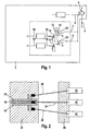
- FIG. 1 shown schematically and in part integrated component 1 is provided for emergency shutdown of the power supply of a brake of a motor vehicle associated valve stages for safety reasons.
- the integrated component 1 includes redundant shutdown paths 2, 2 ', via which one for activation the voltage supply of the valve stages 4 associated driver 6 provided driver output 8 can be pulled to ground if necessary.
- the load drivers, the loads and the shutdown stages can also be present several times.
- the switch-off paths 2, 2 ' are active without switching on and, in order to carry out a switching function as required, in each case comprise a semiconductor switching element 10, 10' designed as a so-called “pull-down transistor". These are switched through by a constant voltage 12.
- the semiconductor switching elements 10, 10 ' is in each case within their Abschaltpfads 2, 2' is also implemented as a transistor, further semiconductor switching element 14, 14 'upstream, which is driven in case of need by a "pull-down deactivation signal 16 and thereby pulls the transistor supply to ground. Consequently, the transistor closes, so that the "pull-down" is deactivated.
- the shutdown paths 2, 2 ' are designed to be completely redundant, with the semiconductor switching elements 10, 10' embodied as transistors in particular being subjected to independent, redundantly designed power supplies.
- the redundancy of the shutdown paths 2, 2 ' is consistently complied with.
- the shutdown paths 2, 2 ' are also secured against crosstalk from short circuits to supply potential.
- the connecting conductor tracks 18, 18 'assigned to the semiconductor switching elements 14, 14' are embodied in the manner of shielded conductors.
- Fig. 2 which on a semiconductor elements also the semiconductor switching elements 10, 10 ', 14, 14' supporting substrate 20 arranged connecting conductor tracks 18, 18 'surrounded by protection zones 22.
- the protection zones 22, which fulfill the function of a protective conductor, are guided adjacent to the connecting conductor tracks 18 and arranged in the assembly plane of the connecting conductor tracks 18.
- a hedge in the direction orthogonal to in Fig. 2 To ensure the placement level shown, the connecting conductor tracks 18 are also surrounded in adjacent assembly levels of suitably selected protection zones.
- the protection zones 22 are durable to ground as a reference potential.
- the connection wire 24 assigned to the connecting conductor 18 and leading from the substrate 20 to the leadframe 26 is also surrounded by protective wires 28 that are durable to ground as the reference potential.
- the semiconductor devices 14, 14 ' surrounded by ground as a reference potential durable protection zones.
- plug contacts 30 connected to the drive control tracks 18, 18 ' are also arranged adjacently in a common plug housing to plug contacts 32, which are grounded as reference potential, so that the entire feed system extending from the plug contact 30 via the connection wire 24 to the connection conductor 18 is shielded ,
- the semiconductor components 14, 14 ' which are provided in particular as so-called MD-OFF transistors, are surrounded by a ground ring (not shown) as a further protection zone.
- a ground ring not shown
- the gate terminal of the semiconductor switching elements 10, 10 'embodied as a transistor is preferably current-limited by a resistor, so that increased safety is ensured in the event of a fault.
- the transistors are preferably NMOS field-effect transistors.
- the "pull-down" resistance of the semiconductor switching elements 10, 10 ' is chosen so small that with the proposed current limit of each redundant switching path can draw such a current and the corresponding line to ground.
Landscapes
- Engineering & Computer Science (AREA)
- Transportation (AREA)
- Mechanical Engineering (AREA)
- Semiconductor Integrated Circuits (AREA)
- Regulating Braking Force (AREA)
- Electronic Switches (AREA)
- Emergency Protection Circuit Devices (AREA)
- Stopping Of Electric Motors (AREA)
- Electric Propulsion And Braking For Vehicles (AREA)
Abstract
Claims (8)
- Composant intégré (1) qui présente plusieurs éléments semi-conducteurs (10, 10', 14, 14') qui branchent et débranchent des pilotes de charge (6) pour des raisons de sécurité,
caractérisé en ce que
des pistes conductrices pilotes (2, 2', 18, 18') associées aux éléments semi-conducteurs (10, 10', 14, 14') sont entourées par des zones de protection (22) maintenues à un potentiel de masse. - Composant intégré (1) selon la revendication 1, caractérisé en ce que des fils de raccordement (24) reliés aux pistes conductrices pilotes (2, 2', 18, 18') sont entourés par des fils de protection (28) qui peuvent être maintenus au potentiel de référence.
- Composant intégré (1) selon les revendications 1 ou 2, caractérisé en ce que chacun des éléments semi-conducteurs (10, 10', 14, 14') est entouré par une zone de protection (22) qui peut être maintenue au potentiel de référence.
- Composant intégré (1) selon l'une des revendications 1 à 3, caractérisé en ce que les fiches de contact (30, 32) reliées aux pistes conductrices pilotes (2, 2', 18, 18') sont disposées dans un boîtier de fiche commun au voisinage des fiches de contact (30, 32) maintenues au potentiel de référence.
- Composant intégré (1) selon l'une des revendications 1 à 4, caractérisé en ce que le potentiel de référence est le potentiel de masse.
- Composant intégré (1) selon l'une des revendications 1 à 5, caractérisé en ce que les éléments semi-conducteurs (10, 10', 14, 14') sont redondants.
- Composant intégré (1) selon l'une des revendications 1 à 6, caractérisé en ce que les éléments semi-conducteurs (10, 10', 14, 14') sont ouverts en l'absence de courant.
- Composant intégré (1) selon l'une des revendications 1 à 7, caractérisé en ce que des conducteurs de commande associés aux éléments semi-conducteurs (10, 10', 14, 14') sont limités en courant.
Applications Claiming Priority (3)
| Application Number | Priority Date | Filing Date | Title |
|---|---|---|---|
| DE10301008 | 2003-01-13 | ||
| DE10301008 | 2003-01-13 | ||
| PCT/EP2003/014155 WO2004062958A2 (fr) | 2003-01-13 | 2003-12-12 | Composant integre |
Publications (2)
| Publication Number | Publication Date |
|---|---|
| EP1587705A2 EP1587705A2 (fr) | 2005-10-26 |
| EP1587705B1 true EP1587705B1 (fr) | 2011-06-15 |
Family
ID=32694887
Family Applications (1)
| Application Number | Title | Priority Date | Filing Date |
|---|---|---|---|
| EP03789252A Expired - Lifetime EP1587705B1 (fr) | 2003-01-13 | 2003-12-12 | Composant integre |
Country Status (6)
| Country | Link |
|---|---|
| EP (1) | EP1587705B1 (fr) |
| JP (1) | JP4431055B2 (fr) |
| KR (1) | KR100983205B1 (fr) |
| CN (1) | CN100379005C (fr) |
| DE (1) | DE10394039D2 (fr) |
| WO (1) | WO2004062958A2 (fr) |
Family Cites Families (4)
| Publication number | Priority date | Publication date | Assignee | Title |
|---|---|---|---|---|
| DE19631627A1 (de) * | 1996-08-05 | 1998-02-12 | Teves Gmbh Alfred | Schaltungsanordnung zur Ansteuerung von Warnsignalgebern |
| US6054780A (en) * | 1997-10-23 | 2000-04-25 | Analog Devices, Inc. | Magnetically coupled signal isolator using a Faraday shielded MR or GMR receiving element |
| WO2002063765A2 (fr) | 2001-02-06 | 2002-08-15 | Koninklijke Philips Electronics N.V. | Tec et circuit de commande integres |
| DE10106359C1 (de) | 2001-02-12 | 2002-09-05 | Hanning Elektro Werke | Laterales Halbleiterbauelement in Dünnfilm-SOI-Technik |
-
2003
- 2003-12-12 JP JP2004565970A patent/JP4431055B2/ja not_active Expired - Fee Related
- 2003-12-12 DE DE10394039T patent/DE10394039D2/de not_active Withdrawn - After Issue
- 2003-12-12 KR KR1020057013003A patent/KR100983205B1/ko not_active Expired - Fee Related
- 2003-12-12 EP EP03789252A patent/EP1587705B1/fr not_active Expired - Lifetime
- 2003-12-12 CN CNB2003801083707A patent/CN100379005C/zh not_active Expired - Fee Related
- 2003-12-12 WO PCT/EP2003/014155 patent/WO2004062958A2/fr not_active Ceased
Also Published As
| Publication number | Publication date |
|---|---|
| JP2006515817A (ja) | 2006-06-08 |
| EP1587705A2 (fr) | 2005-10-26 |
| KR100983205B1 (ko) | 2010-09-20 |
| WO2004062958A2 (fr) | 2004-07-29 |
| KR20050094846A (ko) | 2005-09-28 |
| CN1748311A (zh) | 2006-03-15 |
| DE10394039D2 (de) | 2006-03-23 |
| CN100379005C (zh) | 2008-04-02 |
| JP4431055B2 (ja) | 2010-03-10 |
| WO2004062958A3 (fr) | 2009-04-16 |
Similar Documents
| Publication | Publication Date | Title |
|---|---|---|
| DE69422243T2 (de) | MOS-Ausgangsschaltung mit Schutz gegen Leckströmen | |
| EP0576444B1 (fr) | Etage final d'emetteur integre monolithique | |
| DE69637215T2 (de) | Integrierte Hochspannungsschaltung und Pegelverschiebungseinheit | |
| DE102005039371B4 (de) | Halbleitervorrichtung | |
| DE69430492T2 (de) | Eingangs-Buffer und bidirektionaler Buffer für Systeme mit mehreren Spannungen | |
| DE69327357T2 (de) | Integrierte Halbleiterschaltungsanordnung | |
| EP1289016A2 (fr) | Protection contre les ESDs dans un étage de sortie | |
| EP2300288B1 (fr) | Organe de commande de frein permettant de commander et/ou régler des actionneurs pour influencer une fonction de freinage d un véhicule à moteur | |
| DE112004002717B4 (de) | Pufferschaltung und Pufferschaltungsanordnung mit elektrostatischem Entladeschutz | |
| DE10216015A1 (de) | Überspannungsschutzschaltung | |
| DE69522161T2 (de) | Vorrichtung und Verfahren zum Schutz einer elektrischen Schaltung | |
| EP1212797B1 (fr) | Dispositif de protection contre les decharges electrostatiques pour entrees et sorties de signaux de dispositifs a semi-conducteur avec separation du substrat | |
| EP0396553B1 (fr) | Circuit integre a circuit de production anti-''latch-up'' realise selon la technique des circuits cmos | |
| EP0730332A1 (fr) | Composant semi-conducteur avec structure de projection contre des décharges électrostatiques | |
| DE19706798B4 (de) | Halbleiter-Leistungsmodul | |
| EP1587705B1 (fr) | Composant integre | |
| EP1679746A2 (fr) | Dispositif, circuit et système de protection contre les décharges électrostatiques (ESD) | |
| EP1360726B1 (fr) | Composant à semi-conducteurs comportant une protection contre les décharges électrostatiques | |
| US7196361B1 (en) | Cascoded bi-directional high voltage ESD protection structure | |
| DE102004007655B4 (de) | Halbleiterschaltungen mit ESD-Schutzvorrichtung mit einer mit einem Substrat- oder Guard-Ring-Kontakt kontaktierten ESD-Schutzschaltung | |
| DE102006026691B4 (de) | ESD-Schutzschaltung und -verfahren | |
| EP1503473B1 (fr) | Circuit integré monolithique pour la protection contre les surtensions | |
| DE10014455A1 (de) | Pegelschieber | |
| DE69834321T2 (de) | Halbleiterstruktur für Treiberschaltkreise mit Pegelverschiebung | |
| DE10245654B3 (de) | Treiberschaltung |
Legal Events
| Date | Code | Title | Description |
|---|---|---|---|
| PUAI | Public reference made under article 153(3) epc to a published international application that has entered the european phase |
Free format text: ORIGINAL CODE: 0009012 |
|
| AK | Designated contracting states |
Kind code of ref document: A2 Designated state(s): AT BE BG CH CY CZ DE DK EE ES FI FR GB GR IE IT LI LU MC NL PT SE SK TR |
|
| RBV | Designated contracting states (corrected) |
Designated state(s): DE FR IT |
|
| RIN1 | Information on inventor provided before grant (corrected) |
Inventor name: FEY, WOLFGANG Inventor name: ENGELMANN, MARIO Inventor name: HOELZL, GUNTHER |
|
| PUAK | Availability of information related to the publication of the international search report |
Free format text: ORIGINAL CODE: 0009015 |
|
| RIC1 | Information provided on ipc code assigned before grant |
Ipc: B60L 11/00 20060101AFI20090428BHEP |
|
| 17P | Request for examination filed |
Effective date: 20050816 |
|
| RBV | Designated contracting states (corrected) |
Designated state(s): DE FR IT |
|
| 17Q | First examination report despatched |
Effective date: 20090827 |
|
| GRAP | Despatch of communication of intention to grant a patent |
Free format text: ORIGINAL CODE: EPIDOSNIGR1 |
|
| GRAS | Grant fee paid |
Free format text: ORIGINAL CODE: EPIDOSNIGR3 |
|
| GRAA | (expected) grant |
Free format text: ORIGINAL CODE: 0009210 |
|
| AK | Designated contracting states |
Kind code of ref document: B1 Designated state(s): DE FR IT |
|
| REG | Reference to a national code |
Ref country code: DE Ref legal event code: R096 Ref document number: 50313768 Country of ref document: DE Effective date: 20110721 |
|
| PLBE | No opposition filed within time limit |
Free format text: ORIGINAL CODE: 0009261 |
|
| STAA | Information on the status of an ep patent application or granted ep patent |
Free format text: STATUS: NO OPPOSITION FILED WITHIN TIME LIMIT |
|
| 26N | No opposition filed |
Effective date: 20120316 |
|
| PG25 | Lapsed in a contracting state [announced via postgrant information from national office to epo] |
Ref country code: IT Free format text: LAPSE BECAUSE OF FAILURE TO SUBMIT A TRANSLATION OF THE DESCRIPTION OR TO PAY THE FEE WITHIN THE PRESCRIBED TIME-LIMIT Effective date: 20110615 |
|
| REG | Reference to a national code |
Ref country code: DE Ref legal event code: R097 Ref document number: 50313768 Country of ref document: DE Effective date: 20120316 |
|
| REG | Reference to a national code |
Ref country code: FR Ref legal event code: PLFP Year of fee payment: 13 |
|
| REG | Reference to a national code |
Ref country code: FR Ref legal event code: PLFP Year of fee payment: 14 |
|
| PGFP | Annual fee paid to national office [announced via postgrant information from national office to epo] |
Ref country code: FR Payment date: 20161222 Year of fee payment: 14 |
|
| PGFP | Annual fee paid to national office [announced via postgrant information from national office to epo] |
Ref country code: DE Payment date: 20161231 Year of fee payment: 14 |
|
| REG | Reference to a national code |
Ref country code: DE Ref legal event code: R119 Ref document number: 50313768 Country of ref document: DE |
|
| REG | Reference to a national code |
Ref country code: FR Ref legal event code: ST Effective date: 20180831 |
|
| PG25 | Lapsed in a contracting state [announced via postgrant information from national office to epo] |
Ref country code: FR Free format text: LAPSE BECAUSE OF NON-PAYMENT OF DUE FEES Effective date: 20180102 Ref country code: DE Free format text: LAPSE BECAUSE OF NON-PAYMENT OF DUE FEES Effective date: 20180703 |