EP1587705B1 - Integriertes bauelement - Google Patents
Integriertes bauelement Download PDFInfo
- Publication number
- EP1587705B1 EP1587705B1 EP03789252A EP03789252A EP1587705B1 EP 1587705 B1 EP1587705 B1 EP 1587705B1 EP 03789252 A EP03789252 A EP 03789252A EP 03789252 A EP03789252 A EP 03789252A EP 1587705 B1 EP1587705 B1 EP 1587705B1
- Authority
- EP
- European Patent Office
- Prior art keywords
- integrated component
- semiconductor switching
- switching elements
- surrounded
- reference potential
- Prior art date
- Legal status (The legal status is an assumption and is not a legal conclusion. Google has not performed a legal analysis and makes no representation as to the accuracy of the status listed.)
- Expired - Lifetime
Links
Images
Classifications
-
- B—PERFORMING OPERATIONS; TRANSPORTING
- B60—VEHICLES IN GENERAL
- B60T—VEHICLE BRAKE CONTROL SYSTEMS OR PARTS THEREOF; BRAKE CONTROL SYSTEMS OR PARTS THEREOF, IN GENERAL; ARRANGEMENT OF BRAKING ELEMENTS ON VEHICLES IN GENERAL; PORTABLE DEVICES FOR PREVENTING UNWANTED MOVEMENT OF VEHICLES; VEHICLE MODIFICATIONS TO FACILITATE COOLING OF BRAKES
- B60T17/00—Component parts, details, or accessories of power brake systems not covered by groups B60T8/00, B60T13/00 or B60T15/00, or presenting other characteristic features
-
- H—ELECTRICITY
- H10—SEMICONDUCTOR DEVICES; ELECTRIC SOLID-STATE DEVICES NOT OTHERWISE PROVIDED FOR
- H10W—GENERIC PACKAGES, INTERCONNECTIONS, CONNECTORS OR OTHER CONSTRUCTIONAL DETAILS OF DEVICES COVERED BY CLASS H10
- H10W42/00—Arrangements for protection of devices
- H10W42/80—Arrangements for protection of devices protecting against overcurrent or overload, e.g. fuses or shunts
-
- B—PERFORMING OPERATIONS; TRANSPORTING
- B60—VEHICLES IN GENERAL
- B60T—VEHICLE BRAKE CONTROL SYSTEMS OR PARTS THEREOF; BRAKE CONTROL SYSTEMS OR PARTS THEREOF, IN GENERAL; ARRANGEMENT OF BRAKING ELEMENTS ON VEHICLES IN GENERAL; PORTABLE DEVICES FOR PREVENTING UNWANTED MOVEMENT OF VEHICLES; VEHICLE MODIFICATIONS TO FACILITATE COOLING OF BRAKES
- B60T17/00—Component parts, details, or accessories of power brake systems not covered by groups B60T8/00, B60T13/00 or B60T15/00, or presenting other characteristic features
- B60T17/18—Safety devices; Monitoring
-
- B—PERFORMING OPERATIONS; TRANSPORTING
- B60—VEHICLES IN GENERAL
- B60T—VEHICLE BRAKE CONTROL SYSTEMS OR PARTS THEREOF; BRAKE CONTROL SYSTEMS OR PARTS THEREOF, IN GENERAL; ARRANGEMENT OF BRAKING ELEMENTS ON VEHICLES IN GENERAL; PORTABLE DEVICES FOR PREVENTING UNWANTED MOVEMENT OF VEHICLES; VEHICLE MODIFICATIONS TO FACILITATE COOLING OF BRAKES
- B60T8/00—Arrangements for adjusting wheel-braking force to meet varying vehicular or ground-surface conditions, e.g. limiting or varying distribution of braking force
-
- B—PERFORMING OPERATIONS; TRANSPORTING
- B60—VEHICLES IN GENERAL
- B60T—VEHICLE BRAKE CONTROL SYSTEMS OR PARTS THEREOF; BRAKE CONTROL SYSTEMS OR PARTS THEREOF, IN GENERAL; ARRANGEMENT OF BRAKING ELEMENTS ON VEHICLES IN GENERAL; PORTABLE DEVICES FOR PREVENTING UNWANTED MOVEMENT OF VEHICLES; VEHICLE MODIFICATIONS TO FACILITATE COOLING OF BRAKES
- B60T8/00—Arrangements for adjusting wheel-braking force to meet varying vehicular or ground-surface conditions, e.g. limiting or varying distribution of braking force
- B60T8/32—Arrangements for adjusting wheel-braking force to meet varying vehicular or ground-surface conditions, e.g. limiting or varying distribution of braking force responsive to a speed condition, e.g. acceleration or deceleration
- B60T8/72—Arrangements for adjusting wheel-braking force to meet varying vehicular or ground-surface conditions, e.g. limiting or varying distribution of braking force responsive to a speed condition, e.g. acceleration or deceleration responsive to a difference between a speed condition, e.g. deceleration, and a fixed reference
-
- H—ELECTRICITY
- H10—SEMICONDUCTOR DEVICES; ELECTRIC SOLID-STATE DEVICES NOT OTHERWISE PROVIDED FOR
- H10D—INORGANIC ELECTRIC SEMICONDUCTOR DEVICES
- H10D89/00—Aspects of integrated devices not covered by groups H10D84/00 - H10D88/00
- H10D89/60—Integrated devices comprising arrangements for electrical or thermal protection, e.g. protection circuits against electrostatic discharge [ESD]
-
- H—ELECTRICITY
- H10—SEMICONDUCTOR DEVICES; ELECTRIC SOLID-STATE DEVICES NOT OTHERWISE PROVIDED FOR
- H10W—GENERIC PACKAGES, INTERCONNECTIONS, CONNECTORS OR OTHER CONSTRUCTIONAL DETAILS OF DEVICES COVERED BY CLASS H10
- H10W42/00—Arrangements for protection of devices
- H10W42/20—Arrangements for protection of devices protecting against electromagnetic or particle radiation, e.g. light, X-rays, gamma-rays or electrons
-
- H—ELECTRICITY
- H10—SEMICONDUCTOR DEVICES; ELECTRIC SOLID-STATE DEVICES NOT OTHERWISE PROVIDED FOR
- H10W—GENERIC PACKAGES, INTERCONNECTIONS, CONNECTORS OR OTHER CONSTRUCTIONAL DETAILS OF DEVICES COVERED BY CLASS H10
- H10W44/00—Electrical arrangements for controlling or matching impedance
- H10W44/20—Electrical arrangements for controlling or matching impedance at high-frequency [HF] or radio frequency [RF]
- H10W44/203—Electrical connections
- H10W44/206—Wires
-
- H—ELECTRICITY
- H10—SEMICONDUCTOR DEVICES; ELECTRIC SOLID-STATE DEVICES NOT OTHERWISE PROVIDED FOR
- H10W—GENERIC PACKAGES, INTERCONNECTIONS, CONNECTORS OR OTHER CONSTRUCTIONAL DETAILS OF DEVICES COVERED BY CLASS H10
- H10W70/00—Package substrates; Interposers; Redistribution layers [RDL]
- H10W70/60—Insulating or insulated package substrates; Interposers; Redistribution layers
-
- H—ELECTRICITY
- H10—SEMICONDUCTOR DEVICES; ELECTRIC SOLID-STATE DEVICES NOT OTHERWISE PROVIDED FOR
- H10W—GENERIC PACKAGES, INTERCONNECTIONS, CONNECTORS OR OTHER CONSTRUCTIONAL DETAILS OF DEVICES COVERED BY CLASS H10
- H10W72/00—Interconnections or connectors in packages
- H10W72/50—Bond wires
- H10W72/541—Dispositions of bond wires
- H10W72/5449—Dispositions of bond wires not being orthogonal to a side surface of the chip, e.g. fan-out arrangements
-
- H—ELECTRICITY
- H10—SEMICONDUCTOR DEVICES; ELECTRIC SOLID-STATE DEVICES NOT OTHERWISE PROVIDED FOR
- H10W—GENERIC PACKAGES, INTERCONNECTIONS, CONNECTORS OR OTHER CONSTRUCTIONAL DETAILS OF DEVICES COVERED BY CLASS H10
- H10W90/00—Package configurations
- H10W90/701—Package configurations characterised by the relative positions of pads or connectors relative to package parts
- H10W90/751—Package configurations characterised by the relative positions of pads or connectors relative to package parts of bond wires
- H10W90/754—Package configurations characterised by the relative positions of pads or connectors relative to package parts of bond wires between a chip and a stacked insulating package substrate, interposer or RDL
Definitions
- the invention relates to an integrated component, which can be provided in particular in an integrated circuit for controlling loads in electronic controllers of motor vehicle brakes.
- an electronic brake system For controlling the brakes of a motor vehicle, an electronic brake system may be provided in which valve coils, which are assigned to integrated circuits among other individual brakes, are controlled by means of field-effect transistors.
- a safety shutdown is usually required due to its high relevance for driving safety.
- their functional components are usually additionally secured by redundant circuits.
- a driver output of such a system which is provided to activate the power supply of said valve stages, usually connected so that it can be pulled to ground by two completely redundant shutdown paths if necessary.
- Such redundant shutdown paths are used in integrated circuits that may be integrated into a fault monitoring IC (FMON) that monitors voltages outside of a power driver IC (PCU). If the monitored voltages are outside the specified range, a turn-off transistor is activated via an inverter.
- FMON fault monitoring IC
- PCU power driver IC
- the FMON IC usually consists of two separate blocks, so that if one of these blocks is destroyed, the second block ensures safe shutdown.
- the Abschaltpfade in such an arrangement are usually unswitched active, ie, a so-called “pull-down” transistor is turned on by a constant voltage, wherein another transistor is driven by a so-called “pull-down deactivation signal, thereby pulling the supply of the pull-down transistor to ground.
- the switch-off paths are designed to be completely redundant in such circuits, the particular "pull-down” transistors in particular also being fed via different voltage supplies.
- it can be problematic in such a circuit if a short circuit to the power supply occurs in one of the shutdown paths.
- the source or anode contact and the drain or cathode contact of the power transistor are each drawn via separate shield regions within the substrate, wherein the anode contact is electrically connected to the substrate.
- Shield refers to pn junctions that can be made, for example, by SOI implantation through the silicon film and the buried oxide.
- the anode or the source and the gate contact of a driver transistor and the cathode or the drain contact on two different and mutually floating Shield areas.
- the space charge zone is degraded not only in the thin silicon film and in the buried oxide, but also in the substrate.
- the source contact of the driver transistor is grounded but defined outside the integrated circuit.
- parasitic structures that can transmit interference signals arise between the driver transistors and the power transistors.
- the invention is therefore based on the object, in particular for use for switching on or off of load drivers in a motor vehicle brake system for safety reasons suitable integrated component with a number of semiconductor switching elements indicate, in which a particularly high operational safety is ensured in a particularly simple design ,
- the invention is based on the consideration that, for a particularly high level of operational safety of the integrated component, lateral effects of short circuits in the semiconductor switching elements provided for safety shutdown should be consistently avoided on further semiconductor switching elements connected redundantly therefor.
- the wiring for controlling the semiconductor components should be designed to be particularly secure against such a crosstalk or short circuit. This can be achieved by the connecting conductor tracks assigned to the semiconductor components classified as particularly safety-relevant, such as gate, drain or source terminal conductor tracks, being designed in the manner of a shielded supply line surrounded by a protective conductor.
- the respective connection tracks are surrounded by suitably selected and dimensioned protection zones.
- the protective zones may be, in particular, conductors, conductive surfaces or conductive tracks, which are guided directly adjacent to the connecting track to be protected and are held at a suitable reference potential.
- the protection zones can in this case also include, in particular, adjacently dimensioned and positioned conductive regions arranged in adjacent layers.
- the entire connection area assigned to the respective semiconductor switching elements is embodied in the manner of a shielded supply line.
- advantageously connected to the An horrleiterbahnen connecting wires are surrounded by durable on the reference potential protective wires, which are arranged in alternative or additional advantageous development adjacent to the An horrleiterbahnen plug contacts in a common connector housing adjacent to held on the reference potential plug contacts.
- each of the semiconductor switching elements is expediently surrounded by a protection zone which is durable on the reference potential and is thus shielded.
- control line is advantageously led out of the protective zone surrounding the semiconductor component by the shortest path and at the greatest possible distance from the drain and source terminals.
- the gate terminal is designed in a further advantageous embodiment by a suitably selected resistor current limited.
- a particularly high level of operational safety can be achieved by advantageously providing ground potential as a reference potential.
- the maintenance of ground potential on the protection zones can be achieved in a particularly simple manner by these are suitable and permanently connected to ground line.
- the semiconductor switching elements are advantageously designed redundant. In alternative or additional advantageous Further development, the semiconductor switching elements are normally switched open.
- the advantages achieved by the invention are in particular that the execution of the leads to the safety shutdown provided semiconductor switching elements as a shielded, surrounded by a protective conductor leads a particularly high interpretation-related security against cross-interference of short circuits between the redundant running shutdown paths can be achieved. In this case, an additional protection by external decoupling diodes is not required to ensure high operational safety, so that the integrated component can be made relatively simple.
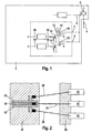
- FIG. 1 shown schematically and in part integrated component 1 is provided for emergency shutdown of the power supply of a brake of a motor vehicle associated valve stages for safety reasons.
- the integrated component 1 includes redundant shutdown paths 2, 2 ', via which one for activation the voltage supply of the valve stages 4 associated driver 6 provided driver output 8 can be pulled to ground if necessary.
- the load drivers, the loads and the shutdown stages can also be present several times.
- the switch-off paths 2, 2 ' are active without switching on and, in order to carry out a switching function as required, in each case comprise a semiconductor switching element 10, 10' designed as a so-called “pull-down transistor". These are switched through by a constant voltage 12.
- the semiconductor switching elements 10, 10 ' is in each case within their Abschaltpfads 2, 2' is also implemented as a transistor, further semiconductor switching element 14, 14 'upstream, which is driven in case of need by a "pull-down deactivation signal 16 and thereby pulls the transistor supply to ground. Consequently, the transistor closes, so that the "pull-down" is deactivated.
- the shutdown paths 2, 2 ' are designed to be completely redundant, with the semiconductor switching elements 10, 10' embodied as transistors in particular being subjected to independent, redundantly designed power supplies.
- the redundancy of the shutdown paths 2, 2 ' is consistently complied with.
- the shutdown paths 2, 2 ' are also secured against crosstalk from short circuits to supply potential.
- the connecting conductor tracks 18, 18 'assigned to the semiconductor switching elements 14, 14' are embodied in the manner of shielded conductors.
- Fig. 2 which on a semiconductor elements also the semiconductor switching elements 10, 10 ', 14, 14' supporting substrate 20 arranged connecting conductor tracks 18, 18 'surrounded by protection zones 22.
- the protection zones 22, which fulfill the function of a protective conductor, are guided adjacent to the connecting conductor tracks 18 and arranged in the assembly plane of the connecting conductor tracks 18.
- a hedge in the direction orthogonal to in Fig. 2 To ensure the placement level shown, the connecting conductor tracks 18 are also surrounded in adjacent assembly levels of suitably selected protection zones.
- the protection zones 22 are durable to ground as a reference potential.
- the connection wire 24 assigned to the connecting conductor 18 and leading from the substrate 20 to the leadframe 26 is also surrounded by protective wires 28 that are durable to ground as the reference potential.
- the semiconductor devices 14, 14 ' surrounded by ground as a reference potential durable protection zones.
- plug contacts 30 connected to the drive control tracks 18, 18 ' are also arranged adjacently in a common plug housing to plug contacts 32, which are grounded as reference potential, so that the entire feed system extending from the plug contact 30 via the connection wire 24 to the connection conductor 18 is shielded ,
- the semiconductor components 14, 14 ' which are provided in particular as so-called MD-OFF transistors, are surrounded by a ground ring (not shown) as a further protection zone.
- a ground ring not shown
- the gate terminal of the semiconductor switching elements 10, 10 'embodied as a transistor is preferably current-limited by a resistor, so that increased safety is ensured in the event of a fault.
- the transistors are preferably NMOS field-effect transistors.
- the "pull-down" resistance of the semiconductor switching elements 10, 10 ' is chosen so small that with the proposed current limit of each redundant switching path can draw such a current and the corresponding line to ground.
Landscapes
- Engineering & Computer Science (AREA)
- Transportation (AREA)
- Mechanical Engineering (AREA)
- Semiconductor Integrated Circuits (AREA)
- Regulating Braking Force (AREA)
- Electronic Switches (AREA)
- Stopping Of Electric Motors (AREA)
- Electric Propulsion And Braking For Vehicles (AREA)
- Emergency Protection Circuit Devices (AREA)
Abstract
Description
- Die Erfindung bezieht sich auf ein integriertes Bauelement, welches insbesondere in einem integrierten Schaltkreis zur Ansteuerung von Lasten in elektronischen Reglern von Kraftfahrzeugbremsen vorgesehen sein kann.
- Zur Regelung der Bremsen eines Kraftfahrzeugs kann ein elektronisches Bremssystem vorgesehen sein, bei dem über integrierte Schaltkreise unter anderem individuellen Bremsen zugeordnete Ventilspulen mittels Feldeffekttransistoren angesteuert werden. Bei Fehlfunktionen eines derartigen Systems ist üblicherweise aufgrund seiner hohen Relevanz für die Fahrsicherheit eine Sicherheitsabschaltung erforderlich. Um deren Zuverlässigkeit in besonders hohem Maße zu gewährleisten, sind ihre Funktionskomponenten üblicherweise durch redundante Schaltkreise zusätzlich abgesichert. Beispielsweise ist ein Treiberausgang eines derartigen Systems, der zur Aktivierung der Spannungsversorgung der genannten Ventilstufen vorgesehen ist, üblicherweise derart verschaltet, dass er im Bedarfsfall durch zwei komplett redundant ausgeführte Abschaltpfade auf Masse gezogen werden kann.
- Derartige redundante Abschaltpfade werden in integrierten Schaltkreisen eingesetzt, die in ein außerhalb eines Leistungstreiber-ICs (PCU) angeordneten Fehlerüberwachungs-IC (FMON), welches Spannungen überwacht, integriert sein können. Geraten die überwachten Spannungen außerhalb des spezifizierten Bereiches, wird ein Abschalttransistor über einen Inverter aktiviert. Das FMON-IC besteht in der Regel aus zwei getrennten Blöcken, so dass bei Zerstörung eines dieser Blöcke der zweite Block ein sicheres Abschalten gewährleistet.
- Die Abschaltpfade in einer derartigen Anordnung sind üblicherweise ungeschaltet aktiv, d. h., ein so genannter "Pulldown"-Transistor wird von einer konstanten Spannung durchgeschaltet, wobei ein weiterer Transistor von einem so genannter "Pulldown"-Deaktivierungssignal angesteuert wird und dabei die Versorgung des "Pulldown"-Transistors auf Masse zieht. Gerade bei der Anwendung in Kraftfahrzeug-Bremssystemen sind in derartigen Schaltungen aus Sicherheitsgründen die Abschaltpfade vollständig redundant ausgelegt, wobei insbesondere auch die genannten "Pulldown"-Transistoren über unterschiedliche Spannungversorgungen bespeist sind. Problematisch kann in einer derartigen Schaltung aber sein, falls bei einem der Abschaltpfade ein Kurzschluss zur Spannungsversorgung auftritt. Dies könnte auch die Funktionsfähigkeit des zweiten Abschaltpfades gefährden, da dieser im Bedarfsfall, also zur funtkionsgerechten Abschaltung des Treiberausgangs, auch die Spannungsver-sorgung auf Masseniveau ziehen müsste. Um dies zu vermeiden, sind die redundanten Abschaltpfade üblicherweise jeweils durch Dioden voneinander entkoppelt.
- Eine derartige Absicherung der Abschaltpfade über Dioden bedingt jedoch einen erhöhten Herstellungs- und Montageaufwand, sowie aufgrund des Spannungsabfalls über die Dioden eine Reduktion des "Pulldown"-Effekts.
- Zur Verminderung von Störsignalen schlägt das Dokument
US2002121664 die monolithische Integration von Treibschaltung, Schutzschaltung und Leistungstransistoren vor. Hierzu wird der Source- bzw. Anoden-Kontakt und der Drain- bzw. Kathoden-Kontakt des Leistungstransistors jeweils über getrennten Shield-Gebieten innerhalb des Substrats gezogen, wobei der Anoden-Kontakt mit dem Substrat elektrisch verbunden ist. Als Shield werden p-n-Übergänge bezeichnet, die z.B. durch SOI-Implantation durch den Silizumfilm und das vergrabene Oxid hindurch hergestellt werden können. Dabei liegen die Anode bzw. der Source- und der Gate-Kontakt eines Treiber-Transistors sowie die Kathode bzw. der Drain-Kontakt auf zwei unterschiedlichen und gegeneinander floatenden Shield-Gebieten. Dadurch wird die Raumladungszone nicht nur im dünnen Siliziumfilm und im vergrabenen Oxid abgebaut, sondern auch im Substrat. Der Source-Kontakt des Treiber-Transistors liegt auf Masse, die jedoch ausserhalb der integrierten Schaltung definiert ist. Trotz der monolithischen Integration entstehen dabei zwischen den Treiber-Transistoren und den Leistungs-Transistoren parasitäre Strukturen, die Störsignale übertragen können. - Der Erfindung liegt daher die Aufgabe zugrunde, ein insbesondere zum Einsatz zum An- oder Abschalten von Lasttreibern in einem Kraftfahrzeug-Bremssystem aus Sicherheitsgründen geeignetes integriertes Bauelement mit einer Anzahl von Halbleiterschaltelementen anzugeben, bei dem bei besonders einfach gehaltener Bauweise eine besonders hohe betriebliche Sicherheit gewährleistet ist.
- Diese Aufgabe wird erfindungsgemäß nach Anspruch 1 dadurch gelöst, dass den Halbleiterschaltelementen zugeordnete Ansteuerleiterbahnen von auf Massepotential gehaltenen Schutzzonen umgeben sind.
- Die Erfindung geht dabei von der Überlegung aus, dass für eine besonders hohe betriebliche Sicherheit des integrierten Bauelements Querauswirkungen von Kurzschlüssen bei den zur Sicherheitsabschaltung vorgesehenen Halbleiterschaltelementen auf dazu redundant geschaltete weitere Halbleiterschaltelemente konsequent vermieden werden sollten. Um dies auf besonders einfache Weise zu erreichen und insbesondere den Einsatz dazu vorgesehener Entkoppel-Dioden entbehrlich zu machen, sollte die Leitungsführung zur Ansteuerung der Halbleiterbauelemente besonders sicher gegenüber einem derartigen Übersprechen oder Kurzschluss ausgeführt sein. Dies ist erreichbar, indem die den als besonders sicherheitsrelevant eingestuften Halbleiterbauelementen zugeordneten Anschlussleiterbahnen, wie beispielsweise Gate-, Drain- oder Source-Anschluss-Leiterbahnen, in der Art einer geschirmten, von einem Schutzleiter umgebenen Zuleitung ausgeführt sind. Dazu sind die jeweiligen Anschluss-leiterbahnen von geeignet gewählten und dimensionierten Schutzzonen umgeben.
- Bei den Schutzzonen kann es sich dabei insbesondere um Leiter, leitende Flächen oder leitende Bahnen handeln, die der zu schützenden Anschlussleiterbahn unmittelbar benachbart geführt sind und auf einem geeigneten Bezugspotential gehalten werden. Bei der Anordnung der Halbleiterbau-elemente in integrierter Bauweise auf einem Substrat können die Schutzzonen dabei insbesondere auch in benachbarten Lagen angeordnete, geeignet dimensionierte und positionierte leitfähige Bereiche umfassen.
- Vorteilhafterweise ist für eine besonders hohe betriebliche Sicherheit der gesamte den jeweiligen Halbleiterschaltelementen zugeordnete Anschlussbereich in der Art einer geschirmten Zuleitung ausgeführt. Dazu sind vorteilhafterweise mit den Ansteuerleiterbahnen verbundene Anschlussdrähte von auf dem Bezugspotential haltbaren Schutzdrähten umgeben, wobei in alternativer oder zusätzlicher vorteilhafter Weiterbildung die mit den Ansteuerleiterbahnen ggf. verbundenen Steckerkontakte in einem gemeinsamen Steckergehäuse zu auf dem Bezugspotential gehaltenen Steckerkontakten benachbart angeordnet sind. Weiterhin ist zweckmäßigerweise jedes der Halbleiterschaltelemente an sich von einer auf dem Bezugspotential haltbaren Schutzzone umgeben und somit geschirmt ausgeführt.
- Bei einer derartigen Anordnung und einer Ausgestaltung des Halbleiterschaltelements als Transistor ist die Steuerleitung (Gate) vorteilhafterweise auf dem kürzesten Weg und in möglichst großem Abstand zu Drain- und Source-Anschlüssen aus der das Halbleiterbauelement umgebenden Schutzzone herausgeführt. Der Gate-Anschluss ist dabei in weiterer vorteilhafter Ausgestaltung durch einen geeignet gewählten Widerstand strombegrenzt ausgeführt.
- Eine besonders hohe betriebliche Sicherheit ist erreichbar, indem als Bezugspotential vorteilhafterweise Massepotential vorgesehen ist. Die Aufrechterhaltung von Massepotential auf den Schutzzonen ist dabei in besonders einfacher Weise erreichbar, indem diese geeignet und dauerhaft mit Masseleitung verbunden sind.
- Um eine hohe betriebliche Sicherheit zu gewährleisten, sind die Halbleiterschaltelemente vorteilhafterweise redundant ausgeführt. In alternativer oder zusatzlicher vorteilhafter Weiterbildung sind die Halbleiterschaltelemente stromlos offen geschaltet.
- Die mit der Erfindung erzielten Vorteile bestehen insbesondere darin, dass durch die Ausführung der Zuleitungen zu den zur Sicherheitsabschaltung vorgesehenen Halbleiterschaltelementen als geschirmte, von einem Schutzleiter umgebene Zuleitungen eine besonders hohe auslegungsbedingte Sicherheit gegen eine Querbeeinflussung von Kurzschlüssen zwischen den redundant ausgeführten Abschaltpfaden erreichbar ist. Dabei ist zur Gewährleistung einer hohen betrieblichen Sicherheit eine zusätzliche Absicherung durch externe Entkoppel-Dioden nicht erforderlich, so dass das integrierte Bauelement vergleichsweise einfach ausgeführt sein kann.
- Ein Ausführungsbeispiel der Erfindung wird anhand einer Zeichnung näher erläutert. Darin zeigen:
- Fig. 1
- ein integriertes Bauelement, insbesondere zur An- wendung in elektronischen Reglern von Kraftfahr- zeugbremssystemen, und
- Fig. 2
- schematisch einen Anschlussbereich des Bauelements nach
Fig. 1 . - Gleiche Teile sind in beiden Figuren mit denselben Bezugszeichen versehen.
- Das in
Fig. 1 schematisch und auszugsweise dargestellte integrierte Bauelement 1 ist zur bedarfsweisen Abschaltung der Spannungsversorgung von einer Bremse eines Kraftfahrzeugs zugeordneten Ventilstufen aus Sicherheitsgründen vorgesehen. Dazu umfasst das integrierte Bauelement 1 redundant ausgeführte Abschaltpfade 2, 2', über die ein zur Aktivierung der Spannungsversorgung des den Ventilstufen 4 zugeordneten Treibers 6 vorgesehener Treiberausgang 8 im Bedarfsfall auf Masse gezogen werden kann. Die Lasttreiber, die Lasten und die Abschaltstufen können selbstverständlich auch mehrfach vorhanden sein. - Die Abschaltpfade 2, 2' sind ungeschaltet aktiv und umfassen zur bedarfsweisen Durchführung einer Schaltfunktion jeweils ein als so genannter "Pulldown"-Transistor ausgeführtes Halbleiterschaltelement 10, 10'. Diese werden von einer konstanten Spannung 12 durchgeschaltet. Den Halbleiterschaltelementen 10, 10' ist jeweils innerhalb ihres Abschaltpfads 2, 2' ein ebenfalls als Transistor ausgeführtes, weiteres Halbleiterschaltelement 14, 14' vorgeschaltet, das im Bedarfsfall von einem "Pulldown"-Deaktivierungssignal 16 angesteuert wird und dabei die Transistorversorgung auf Masse zieht. Der Transistor schließt demzufolge, so dass der "Pulldown" deaktiviert ist.
- Aus Sicherheitsgründen sind die Abschaltpfade 2, 2' vollständig redundant ausgeführt, wobei insbesondere die als Transistoren ausgeführten Halbleiterschaltelemente 10, 10' mit unabhängigen, redundant ausgeführten Spannungsversorgungen beaufschlagt sind.
- Für eine besonders hohe betriebliche Sicherheit ist die Redundanz der Abschaltpfade 2, 2' konsequent eingehalten. Dabei sind die Abschaltpfade 2, 2' auch gegen ein Übersprechen von Kurzschlüssen gegen Versorgungspotential abge-sichert. Um dies mit einfacher Bauweise und insbesondere unter Verzicht auf die Verwendung externer Entkoppel-Dioden zu gewährleisten, sind die den Halbleiterschaltelementen 14, 14' zugeordneten Anschlussleiterbahnen 18, 18' in der Art geschirmter Leiter ausgeführt.
- Dazu sind, wie dies im Ausschnitt nach
Fig. 2 erkennbar ist, die auf einem auch die Halbleiterschaltelemente 10, 10', 14, 14' tragenden Substrat 20 angeordneten Anschlussleiterbahnen 18, 18' von Schutzzonen 22 umgeben. Die Schutzzonen 22, die die Funktion eines Schutzleiters erfüllen, sind dabei zu den Anschlussleiterbahnen 18 benachbart geführt und in der Bestückungsebene der Anschlussleiterbahnen 18 angeordnet. Um zudem auch eine Absicherung in Richtung orthogonal zur inFig. 2 gezeigten Bestückungsebene zu gewährleisten, sind die Anschlussleiterbahnen 18 auch in benachbarten Bestückungsebenen von geeignet gewählten Schutzzonen umgeben. - Die Schutzzonen 22 sind auf Masse als Bezugspotential haltbar. In der Art einer vollständigen Schirmung ist aber auch der der Anschlussleiterbahn 18 zugeordnete Anschlussdraht 24, der vom Substrat 20 zum Leadframe 26 führt, von auf Masse als Bezugspotential haltbaren Schutzdrähten 28 umgeben. In nicht näher dargestellter Weise sind zudem die Halbleiterbauelemente 14, 14' von auf Masse als Bezugspotential haltbaren Schutzzonen umgeben.
- Die mit den Ansteuerleiterbahnen 18, 18' verbundenen Steckerkontakte 30 sind zudem in einem gemeinsamem Steckergehäuse zu auf Masse als Bezugspotential gehaltenen Steckerkontakten 32 benachbart angeordnet, so dass das gesamte, sich vom Steckerkontakt 30 über den Anschlussdraht 24 bis zur Anschlussleiterbahn 18 erstreckende Zuleitungssystem geschirmt ausgeführt ist.
- Die insbesondere als so genannte MD-OFF-Transistoren vorgesehenen Halbleiterbauelemente 14, 14' sind von einem nicht näher dargestellten Massering als weitere Schutzzone umgeben. Zusätzlich ist es zweckmäßig, die Steuerleitung (Gate) auf dem kürzesten Weg und in möglichst großem Abstand zu Drain- und Source-Anschlüssen aus diesem Ring herauszuführen.
- Der Gate-Anschluss der als Transistor ausgeführten Halbleiterschaltelemente 10, 10' ist bevorzugt durch einen Widerstand strombegrenzt, so dass im Fehlerfall erhöhte Sicherheit gewährleistet ist. Bei den Transistoren handelt es sich vorzugsweise um NMOS-Feldeffekttransistoren.
- Der "Pulldown"-Widerstand der Halbleiterschaltelemente 10, 10' ist dabei derart gering gewählt, dass mit der vorgesehenen Strombegrenzung der jeweils redundante Schaltpfad einen solchen Strom sowie die entsprechende Leitung auf Masse ziehen kann.
-
- 1
- Bauelement
- 2, 2'
- Abschaltpfade
- 4
- Ventilstufen
- 6
- Treiber
- 8
- Treiberausgang
- 10, 10'
- Halbleiterschaltelement
- 12
- Spannung
- 14, 14'
- Halbleiterschaltelement
- 16
- "Pulldown"-Deaktivierungssignal
- 18, 18'
- Anschlussleiterbahn
- 20
- Substrat
- 22
- Schutzzone
- 24
- Anschlussdraht
- 26
- Leadframe
- 28
- Schutzdrähte
- 30, 32
- Steckerkontakte
Claims (8)
- Integriertes Bauelement (1) mit einer Anzahl von Halbleiterschaltelementen (10, 10', 14, 14') zum An- oder Abschalten von Lasttreibern (6) aus Sicherheitsgründen, dadurch gekennzeichnet, dass den Halbleiterschaltelementen (10, 10', 14, 14') zugeordnete Ansteuerleiterbahnen (2, 2', 18, 18') von auf Massepotential gehaltenen Schutzzonen (22) umgeben sind.
- Integriertes Bauelement (1) nach Anspruch 1, dadurch gekennzeichnet, dass mit den Ansteuerleiterbahnen (2, 2', 18, 18') verbundene Anschlussdrähte (24) von auf dem Bezugspotential haltbaren Schutzdrähten (28) umgeben sind.
- Integriertes Bauelement (1) nach Anspruch 1 oder 2, dadurch gekennzeichnet, dass jedes der Halbleiterschaltelemente (10, 10', 14, 14') von einer auf dem Bezugspotential haltbaren Schutzzone (22) umgeben ist.
- Integriertes Bauelement (1) nach einem der Ansprüche 1 bis 3, dadurch gekennzeichnet, dass die mit den Ansteuerleiterbahnen (2, 2', 18, 18') verbundenen Steckerkontakte (30, 32) in einem gemeinsamen Steckergehäuse zu auf dem Bezugspotential gehaltenen Steckerkontakten (30, 32) benachbart angeordnet sind.
- Integriertes Bauelement (1) nach einem der Ansprüche 1 bis 4, dadurch gekennzeichnet, dass als Bezugspotential Massepotential vorgesehen ist.
- Integriertes Bauelement (1) nach einem der Ansprüche 1 bis 5, dadurch gekennzeichnet, dass die Halbleiterschaltelemente (10, 10', 14, 14') redundant ausgeführt sind.
- Integriertes Bauelement (1) nach einem der Ansprüche 1 bis 6, dadurch gekennzeichnet, dass die Halbleiterschaltelemente (10, 10', 14, 14') stromlos offen geschaltet sind.
- Integriertes Bauelement (1) nach einem der Ansprüche 1 bis 7, dadurch gekennzeichnet, dass den Halbleiterschaltelementen (10, 10', 14, 14') zugeordnete Steuerletiungen strombegrenzt sind.
Applications Claiming Priority (3)
| Application Number | Priority Date | Filing Date | Title |
|---|---|---|---|
| DE10301008 | 2003-01-13 | ||
| DE10301008 | 2003-01-13 | ||
| PCT/EP2003/014155 WO2004062958A2 (de) | 2003-01-13 | 2003-12-12 | Integriertes bauelement |
Publications (2)
| Publication Number | Publication Date |
|---|---|
| EP1587705A2 EP1587705A2 (de) | 2005-10-26 |
| EP1587705B1 true EP1587705B1 (de) | 2011-06-15 |
Family
ID=32694887
Family Applications (1)
| Application Number | Title | Priority Date | Filing Date |
|---|---|---|---|
| EP03789252A Expired - Lifetime EP1587705B1 (de) | 2003-01-13 | 2003-12-12 | Integriertes bauelement |
Country Status (6)
| Country | Link |
|---|---|
| EP (1) | EP1587705B1 (de) |
| JP (1) | JP4431055B2 (de) |
| KR (1) | KR100983205B1 (de) |
| CN (1) | CN100379005C (de) |
| DE (1) | DE10394039D2 (de) |
| WO (1) | WO2004062958A2 (de) |
Family Cites Families (4)
| Publication number | Priority date | Publication date | Assignee | Title |
|---|---|---|---|---|
| DE19631627A1 (de) * | 1996-08-05 | 1998-02-12 | Teves Gmbh Alfred | Schaltungsanordnung zur Ansteuerung von Warnsignalgebern |
| US6054780A (en) * | 1997-10-23 | 2000-04-25 | Analog Devices, Inc. | Magnetically coupled signal isolator using a Faraday shielded MR or GMR receiving element |
| WO2002063765A2 (en) | 2001-02-06 | 2002-08-15 | Koninklijke Philips Electronics N.V. | Integrated fet and driver |
| DE10106359C1 (de) * | 2001-02-12 | 2002-09-05 | Hanning Elektro Werke | Laterales Halbleiterbauelement in Dünnfilm-SOI-Technik |
-
2003
- 2003-12-12 WO PCT/EP2003/014155 patent/WO2004062958A2/de not_active Ceased
- 2003-12-12 JP JP2004565970A patent/JP4431055B2/ja not_active Expired - Fee Related
- 2003-12-12 KR KR1020057013003A patent/KR100983205B1/ko not_active Expired - Fee Related
- 2003-12-12 EP EP03789252A patent/EP1587705B1/de not_active Expired - Lifetime
- 2003-12-12 CN CNB2003801083707A patent/CN100379005C/zh not_active Expired - Fee Related
- 2003-12-12 DE DE10394039T patent/DE10394039D2/de not_active Withdrawn - After Issue
Also Published As
| Publication number | Publication date |
|---|---|
| KR20050094846A (ko) | 2005-09-28 |
| JP4431055B2 (ja) | 2010-03-10 |
| WO2004062958A3 (de) | 2009-04-16 |
| CN100379005C (zh) | 2008-04-02 |
| DE10394039D2 (de) | 2006-03-23 |
| CN1748311A (zh) | 2006-03-15 |
| EP1587705A2 (de) | 2005-10-26 |
| WO2004062958A2 (de) | 2004-07-29 |
| KR100983205B1 (ko) | 2010-09-20 |
| JP2006515817A (ja) | 2006-06-08 |
Similar Documents
| Publication | Publication Date | Title |
|---|---|---|
| EP0576444B1 (de) | Monolithisch integrierte senderendstufe | |
| DE69637215T2 (de) | Integrierte Hochspannungsschaltung und Pegelverschiebungseinheit | |
| DE102005039371B4 (de) | Halbleitervorrichtung | |
| DE69327357T2 (de) | Integrierte Halbleiterschaltungsanordnung | |
| EP1289016A2 (de) | ESD Schutz für CMOS-Ausgangsstufe | |
| EP2300288B1 (de) | Bremsensteuergerät zur ansteuerung und/oder regelung von aktuatoren zur beeinflussung einer bremsfunktion eines kraftfahrzeugs | |
| DE112004002717B4 (de) | Pufferschaltung und Pufferschaltungsanordnung mit elektrostatischem Entladeschutz | |
| DE10216015A1 (de) | Überspannungsschutzschaltung | |
| DE69522161T2 (de) | Vorrichtung und Verfahren zum Schutz einer elektrischen Schaltung | |
| EP0736904A1 (de) | Integrierte Halbleiterschaltung mit einem Schutzmittel | |
| EP1212797B1 (de) | Esd-schutzanordnung für signaleingänge und -ausgänge bei halbleitervorrichtungen mit substrattrennung | |
| EP0396553B1 (de) | Integrierte schaltung mit ''latch-up''-schutzschaltung in komplementärer mos-schaltungstechnik | |
| EP0730332A1 (de) | Halbleiterbauelement mit Schutzstruktur zum Schutz vor elektrostatischer Entladung | |
| DE19706798B4 (de) | Halbleiter-Leistungsmodul | |
| EP1679746A2 (de) | Vorrichtung, Anordnung und System zum ESD-Schutz | |
| EP1360726B1 (de) | Halbleiter-Bauelement mit ESD-Schutz | |
| US7196361B1 (en) | Cascoded bi-directional high voltage ESD protection structure | |
| DE102004007655B4 (de) | Halbleiterschaltungen mit ESD-Schutzvorrichtung mit einer mit einem Substrat- oder Guard-Ring-Kontakt kontaktierten ESD-Schutzschaltung | |
| DE4423733C2 (de) | Integriertes Leistungs-Halbleiterbauelement mit Schutzstruktur | |
| DE102006026691B4 (de) | ESD-Schutzschaltung und -verfahren | |
| EP1587705A2 (de) | Integriertes bauelement | |
| EP1503473B1 (de) | Monolithisch integrierbare Schaltungsanordnung zum Überspannungsschutz | |
| DE10014455A1 (de) | Pegelschieber | |
| DE69834321T2 (de) | Halbleiterstruktur für Treiberschaltkreise mit Pegelverschiebung | |
| DE10245654B3 (de) | Treiberschaltung |
Legal Events
| Date | Code | Title | Description |
|---|---|---|---|
| PUAI | Public reference made under article 153(3) epc to a published international application that has entered the european phase |
Free format text: ORIGINAL CODE: 0009012 |
|
| AK | Designated contracting states |
Kind code of ref document: A2 Designated state(s): AT BE BG CH CY CZ DE DK EE ES FI FR GB GR IE IT LI LU MC NL PT SE SK TR |
|
| RBV | Designated contracting states (corrected) |
Designated state(s): DE FR IT |
|
| RIN1 | Information on inventor provided before grant (corrected) |
Inventor name: FEY, WOLFGANG Inventor name: ENGELMANN, MARIO Inventor name: HOELZL, GUNTHER |
|
| PUAK | Availability of information related to the publication of the international search report |
Free format text: ORIGINAL CODE: 0009015 |
|
| RIC1 | Information provided on ipc code assigned before grant |
Ipc: B60L 11/00 20060101AFI20090428BHEP |
|
| 17P | Request for examination filed |
Effective date: 20050816 |
|
| RBV | Designated contracting states (corrected) |
Designated state(s): DE FR IT |
|
| 17Q | First examination report despatched |
Effective date: 20090827 |
|
| GRAP | Despatch of communication of intention to grant a patent |
Free format text: ORIGINAL CODE: EPIDOSNIGR1 |
|
| GRAS | Grant fee paid |
Free format text: ORIGINAL CODE: EPIDOSNIGR3 |
|
| GRAA | (expected) grant |
Free format text: ORIGINAL CODE: 0009210 |
|
| AK | Designated contracting states |
Kind code of ref document: B1 Designated state(s): DE FR IT |
|
| REG | Reference to a national code |
Ref country code: DE Ref legal event code: R096 Ref document number: 50313768 Country of ref document: DE Effective date: 20110721 |
|
| PLBE | No opposition filed within time limit |
Free format text: ORIGINAL CODE: 0009261 |
|
| STAA | Information on the status of an ep patent application or granted ep patent |
Free format text: STATUS: NO OPPOSITION FILED WITHIN TIME LIMIT |
|
| 26N | No opposition filed |
Effective date: 20120316 |
|
| PG25 | Lapsed in a contracting state [announced via postgrant information from national office to epo] |
Ref country code: IT Free format text: LAPSE BECAUSE OF FAILURE TO SUBMIT A TRANSLATION OF THE DESCRIPTION OR TO PAY THE FEE WITHIN THE PRESCRIBED TIME-LIMIT Effective date: 20110615 |
|
| REG | Reference to a national code |
Ref country code: DE Ref legal event code: R097 Ref document number: 50313768 Country of ref document: DE Effective date: 20120316 |
|
| REG | Reference to a national code |
Ref country code: FR Ref legal event code: PLFP Year of fee payment: 13 |
|
| REG | Reference to a national code |
Ref country code: FR Ref legal event code: PLFP Year of fee payment: 14 |
|
| PGFP | Annual fee paid to national office [announced via postgrant information from national office to epo] |
Ref country code: FR Payment date: 20161222 Year of fee payment: 14 |
|
| PGFP | Annual fee paid to national office [announced via postgrant information from national office to epo] |
Ref country code: DE Payment date: 20161231 Year of fee payment: 14 |
|
| REG | Reference to a national code |
Ref country code: DE Ref legal event code: R119 Ref document number: 50313768 Country of ref document: DE |
|
| REG | Reference to a national code |
Ref country code: FR Ref legal event code: ST Effective date: 20180831 |
|
| PG25 | Lapsed in a contracting state [announced via postgrant information from national office to epo] |
Ref country code: FR Free format text: LAPSE BECAUSE OF NON-PAYMENT OF DUE FEES Effective date: 20180102 Ref country code: DE Free format text: LAPSE BECAUSE OF NON-PAYMENT OF DUE FEES Effective date: 20180703 |