EP1587684B1 - Verkleinerter heizchip für einen tintenstrahldruckkopf mit integriertem spannungsregler und drehkondensatorenregelkondensatoren - Google Patents
Verkleinerter heizchip für einen tintenstrahldruckkopf mit integriertem spannungsregler und drehkondensatorenregelkondensatoren Download PDFInfo
- Publication number
- EP1587684B1 EP1587684B1 EP03800175A EP03800175A EP1587684B1 EP 1587684 B1 EP1587684 B1 EP 1587684B1 EP 03800175 A EP03800175 A EP 03800175A EP 03800175 A EP03800175 A EP 03800175A EP 1587684 B1 EP1587684 B1 EP 1587684B1
- Authority
- EP
- European Patent Office
- Prior art keywords
- voltage
- volts
- heater chip
- fet
- input
- Prior art date
- Legal status (The legal status is an assumption and is not a legal conclusion. Google has not performed a legal analysis and makes no representation as to the accuracy of the status listed.)
- Expired - Lifetime
Links
Images


Classifications
-
- B—PERFORMING OPERATIONS; TRANSPORTING
- B41—PRINTING; LINING MACHINES; TYPEWRITERS; STAMPS
- B41J—TYPEWRITERS; SELECTIVE PRINTING MECHANISMS, i.e. MECHANISMS PRINTING OTHERWISE THAN FROM A FORME; CORRECTION OF TYPOGRAPHICAL ERRORS
- B41J2/00—Typewriters or selective printing mechanisms characterised by the printing or marking process for which they are designed
- B41J2/005—Typewriters or selective printing mechanisms characterised by the printing or marking process for which they are designed characterised by bringing liquid or particles selectively into contact with a printing material
- B41J2/01—Ink jet
- B41J2/015—Ink jet characterised by the jet generation process
- B41J2/04—Ink jet characterised by the jet generation process generating single droplets or particles on demand
- B41J2/045—Ink jet characterised by the jet generation process generating single droplets or particles on demand by pressure, e.g. electromechanical transducers
- B41J2/04501—Control methods or devices therefor, e.g. driver circuits, control circuits
- B41J2/04521—Control methods or devices therefor, e.g. driver circuits, control circuits reducing number of signal lines needed
-
- B—PERFORMING OPERATIONS; TRANSPORTING
- B41—PRINTING; LINING MACHINES; TYPEWRITERS; STAMPS
- B41J—TYPEWRITERS; SELECTIVE PRINTING MECHANISMS, i.e. MECHANISMS PRINTING OTHERWISE THAN FROM A FORME; CORRECTION OF TYPOGRAPHICAL ERRORS
- B41J2/00—Typewriters or selective printing mechanisms characterised by the printing or marking process for which they are designed
- B41J2/005—Typewriters or selective printing mechanisms characterised by the printing or marking process for which they are designed characterised by bringing liquid or particles selectively into contact with a printing material
- B41J2/01—Ink jet
- B41J2/015—Ink jet characterised by the jet generation process
- B41J2/04—Ink jet characterised by the jet generation process generating single droplets or particles on demand
- B41J2/045—Ink jet characterised by the jet generation process generating single droplets or particles on demand by pressure, e.g. electromechanical transducers
- B41J2/04501—Control methods or devices therefor, e.g. driver circuits, control circuits
- B41J2/04541—Specific driving circuit
-
- B—PERFORMING OPERATIONS; TRANSPORTING
- B41—PRINTING; LINING MACHINES; TYPEWRITERS; STAMPS
- B41J—TYPEWRITERS; SELECTIVE PRINTING MECHANISMS, i.e. MECHANISMS PRINTING OTHERWISE THAN FROM A FORME; CORRECTION OF TYPOGRAPHICAL ERRORS
- B41J2/00—Typewriters or selective printing mechanisms characterised by the printing or marking process for which they are designed
- B41J2/005—Typewriters or selective printing mechanisms characterised by the printing or marking process for which they are designed characterised by bringing liquid or particles selectively into contact with a printing material
- B41J2/01—Ink jet
- B41J2/015—Ink jet characterised by the jet generation process
- B41J2/04—Ink jet characterised by the jet generation process generating single droplets or particles on demand
- B41J2/045—Ink jet characterised by the jet generation process generating single droplets or particles on demand by pressure, e.g. electromechanical transducers
- B41J2/04501—Control methods or devices therefor, e.g. driver circuits, control circuits
- B41J2/04543—Block driving
-
- B—PERFORMING OPERATIONS; TRANSPORTING
- B41—PRINTING; LINING MACHINES; TYPEWRITERS; STAMPS
- B41J—TYPEWRITERS; SELECTIVE PRINTING MECHANISMS, i.e. MECHANISMS PRINTING OTHERWISE THAN FROM A FORME; CORRECTION OF TYPOGRAPHICAL ERRORS
- B41J2/00—Typewriters or selective printing mechanisms characterised by the printing or marking process for which they are designed
- B41J2/005—Typewriters or selective printing mechanisms characterised by the printing or marking process for which they are designed characterised by bringing liquid or particles selectively into contact with a printing material
- B41J2/01—Ink jet
- B41J2/015—Ink jet characterised by the jet generation process
- B41J2/04—Ink jet characterised by the jet generation process generating single droplets or particles on demand
- B41J2/045—Ink jet characterised by the jet generation process generating single droplets or particles on demand by pressure, e.g. electromechanical transducers
- B41J2/04501—Control methods or devices therefor, e.g. driver circuits, control circuits
- B41J2/04548—Details of power line section of control circuit
-
- B—PERFORMING OPERATIONS; TRANSPORTING
- B41—PRINTING; LINING MACHINES; TYPEWRITERS; STAMPS
- B41J—TYPEWRITERS; SELECTIVE PRINTING MECHANISMS, i.e. MECHANISMS PRINTING OTHERWISE THAN FROM A FORME; CORRECTION OF TYPOGRAPHICAL ERRORS
- B41J2/00—Typewriters or selective printing mechanisms characterised by the printing or marking process for which they are designed
- B41J2/005—Typewriters or selective printing mechanisms characterised by the printing or marking process for which they are designed characterised by bringing liquid or particles selectively into contact with a printing material
- B41J2/01—Ink jet
- B41J2/015—Ink jet characterised by the jet generation process
- B41J2/04—Ink jet characterised by the jet generation process generating single droplets or particles on demand
- B41J2/045—Ink jet characterised by the jet generation process generating single droplets or particles on demand by pressure, e.g. electromechanical transducers
- B41J2/04501—Control methods or devices therefor, e.g. driver circuits, control circuits
- B41J2/0457—Power supply level being detected or varied
-
- B—PERFORMING OPERATIONS; TRANSPORTING
- B41—PRINTING; LINING MACHINES; TYPEWRITERS; STAMPS
- B41J—TYPEWRITERS; SELECTIVE PRINTING MECHANISMS, i.e. MECHANISMS PRINTING OTHERWISE THAN FROM A FORME; CORRECTION OF TYPOGRAPHICAL ERRORS
- B41J2/00—Typewriters or selective printing mechanisms characterised by the printing or marking process for which they are designed
- B41J2/005—Typewriters or selective printing mechanisms characterised by the printing or marking process for which they are designed characterised by bringing liquid or particles selectively into contact with a printing material
- B41J2/01—Ink jet
- B41J2/015—Ink jet characterised by the jet generation process
- B41J2/04—Ink jet characterised by the jet generation process generating single droplets or particles on demand
- B41J2/045—Ink jet characterised by the jet generation process generating single droplets or particles on demand by pressure, e.g. electromechanical transducers
- B41J2/04501—Control methods or devices therefor, e.g. driver circuits, control circuits
- B41J2/0458—Control methods or devices therefor, e.g. driver circuits, control circuits controlling heads based on heating elements forming bubbles
-
- B—PERFORMING OPERATIONS; TRANSPORTING
- B41—PRINTING; LINING MACHINES; TYPEWRITERS; STAMPS
- B41J—TYPEWRITERS; SELECTIVE PRINTING MECHANISMS, i.e. MECHANISMS PRINTING OTHERWISE THAN FROM A FORME; CORRECTION OF TYPOGRAPHICAL ERRORS
- B41J2/00—Typewriters or selective printing mechanisms characterised by the printing or marking process for which they are designed
- B41J2/005—Typewriters or selective printing mechanisms characterised by the printing or marking process for which they are designed characterised by bringing liquid or particles selectively into contact with a printing material
- B41J2/01—Ink jet
- B41J2/17—Ink jet characterised by ink handling
- B41J2/175—Ink supply systems ; Circuit parts therefor
- B41J2/17503—Ink cartridges
- B41J2/17526—Electrical contacts to the cartridge
Definitions
- a thermal inkjet printhead includes access to a local or remote supply of color or mono ink, a heater chip, a nozzle or orifice plate attached to the heater chip, and an input/output connector, such as a tape automated bond (TAB) circuit, for electrically connecting the heater chip to the printer during use.
- the heater chip typically includes a plurality of thin film resistors or heaters fabricated by deposition, masking and etching techniques on a substrate such as silicon.
- an individual resistive heater is uniquely addressed with a small amount of current to rapidly heat a small volume of ink. This causes the ink to vaporize in a local ink chamber (between the heater and nozzle plate) and be ejected through and projected by the nozzle plate towards the print medium.
- the circuitry that drives the printing of a single ink drop typically includes a source of a field effect transistor (FET) and a voltage source (+10.8 volts is common) coupled to either ends of the resistive heater.
- Control logic circuitry sends logic signals to a gate of the FET and, upon actuation of the FET, the resistive heater heats and ink is ejected.
- the heater chip has an integral voltage regulator that derives two output voltages from a single voltage input to the chip.
- One of the two output voltages powers control logic circuitry while the other powers FET drivers.
- the input voltage includes +10.8 volts and the output voltages include lines of +3.3 volts for the control logic circuitry and +7.5 volts for the FET drivers.
- a Vgs of the FET is about +7.5 volts which enables a FET area width of about 400 microns and an area length of about 42 microns (1/600 th inch).
- Outputs of the control circuitry provide input to the FET drivers.
- a resistive heater for ejecting ink couples between a drain of the FET and the chip input voltage.
- Preferred FET drivers include logic AND gates or logic NAND gates with an inverter.
- Printheads containing the heater chip and printers containing the printhead are also disclosed.
- inkjet printhead heater chip having a reduced size due to narrowed-width power FETs driven by an integral voltage regulator with regulating capacitors.
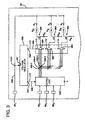
- Ink drops from compartment 16 are caused to be eject from the heater chip 25 at such times pursuant to commands of a printer microprocessor or other controller 57.
- the timing of the ink drop emissions corresponds to a pattern of pixels of the image being printed. Often times, such patterns become generated in devices electrically connected to the controller 57 (via Ext. input) that reside externally to the printer and include, but are not limited to, a computer, a scanner, a camera, a visual display unit, a personal data assistant, or other.
- a control panel 58 having user selection interface 60 also accompanies many printers, as an input 62 to the controller 57, to provide additional printer capabilities and robustness.
- the control logic circuit 340 the drivers 350 and the resistive heater elements R H , the first and second output voltage lines 336, 338 of the voltage regulator 330 supply voltages to the control logic circuit and the drivers, respectively, while the input voltage from input terminal 28 1 supplies voltage to the resistive heaters.
- the control logic circuit can receive one voltage for CMOS-based logic devices and the drivers can simultaneously receive another voltage while only one voltage is supplied to the heater chip.
- the voltage on line 336 is about +3.3 volts while the voltage on line 338 is about +7.5 volts.
- a Vgs (gate to source voltage) of the FET can become as large as about +7.5 volts.
- the voltage reference circuit 500 comprises a voltage divider consisting of a pair of resistors R6, R7 in series. The ratio of the two resistors is selected to achieve a desired reference voltage at a node 1 between them.
- R6 is a 150 K ohm resistor
- R7 is a 66 K ohm resistor and since the input voltage is about 10.8 volts, a reference voltage of about 3.3 volts is achieved.
- a capacitor C3 may be provided to assist in stabilizing the voltage.
- One preferred C3 value is 200 pF.
- the regulator circuit 520 is similar to regulator circuit 510 except that a resistor R4 (125 K ohm) is added between the non-inverting input (-) of the op-amp 522 and a drain of the pass device 524. In turn, amplifier gain increases such that an output of the op-amp 522 attempts to hold the voltage at node 335 at a constant 7.5 volts.
- the value of the loading resistor R5 (30 K ohm) has also been modified to provide the same constant 250 A of current flow.
- Preferred etching techniques include, but are not limited to, any variety of wet or dry etches, reactive ion etches, deep reactive ion etches, etc.
- Preferred photolithography steps include, but are not limited to, exposure to ultraviolet or x-ray light sources, or other, and photomasking includes photomasking islands and/or photomasking holes. The particular embodiment, island or hole, depends upon whether the configuration of the mask is a clear-field or dark-field mask as those terms are well understood in the art.
- the input and output voltages of the voltage regulator could be any value other than those 10, 10.8, 3.3 and 7.5 volt values described.
- the switch could be any switch other than a transistor or a transistor, such as npn, pnp, bi-polar transistor, n-channel, p-channel or dual channel JFET, MOSFET, IGFET, or other, instead of just the power FETs shown.
- the input terminals of the heater chip could comprise wires, bumps, or other instead of the bond pads shown.
Landscapes
- Particle Formation And Scattering Control In Inkjet Printers (AREA)
Claims (9)
- Heizchip (25) für einen Tintenstrahl-Druckkopf (10), der enthält:einen Eingangsanschluss (28) zum Empfangen einer Eingangsspannung;einen Spannungsregler (13), der an den Eingangsanschluss gekoppelt ist und der eine erste (336) und eine zweite (338) Ausgangsspannungsleitung mit Spannungen besitzt, die während der Benutzung von der Eingangsspannung abgeleitet werden;einen Treiber (350), der an eine der ersten (336) und der zweiten (338) Ausgangsspannungsleitung gekoppelt ist, um eine Speisespannung zu empfangen;eine Steuerlogikschaltung (340), die an den Treiber und an die andere der ersten (336) und der zweiten (338) Ausgangsspannungsleitung gekoppelt ist, um die Speisespannung zu empfangen;einen Transistor, der an den Treiber gekoppelt ist; undein Widerstandsheizelement, das an den Transistor und an den Eingangsanschluss zum Empfangen der Speisespannung von der Eingangsspannung gekoppelt ist.
- Heizchip (25) nach Anspruch 1, wobei während der Benutzung eine der ersten und der zweiten Ausgangsspannungsleitung etwa 3,3 Volt aufweist, während die andere der ersten und der zweiten Ausgangsspannungsleitung etwa 7,5 Volt aufweist.
- Heizchip (25) nach Anspruch 1, wobei während der Benutzung die Eingangsspannung etwa 10,8 Volt beträgt.
- Heizchip (25) nach Anspruch 1, wobei der Eingangsanschluss ein Bond-Pad (28) ist.
- Heizchip (25) nach Anspruch 1, wobei eine Bereichsbreite des Transistors etwa 400 µm beträgt.
- Verfahren zum Betreiben eines Heizchips (25) eines Tintenstrahl-Druckkopfs (10), das enthält:Liefern einer Eingangsspannung an einen Spannungsregler (330);Ableiten wenigstens einer ersten (336) und einer zweiten (338) Ausgangsspannung von der Eingangsspannung, wobei das Ableiten durch den Spannungsregler (330) ausgeführt wird;Liefern einer der ersten und der zweiten Ausgangsspannung an einen Treiber (350);Aktivieren eines an den Treiber (350) gekoppelten Schalters durch eine Ausgabe des Treibers; undLiefern der Eingangsspannung an ein Widerstandsheizelement, das an einen Ausgang des Schalters gekoppelt ist;und das ferner das Liefern der anderen der ersten und der zweiten Ausgangsspannung an eine Steuerlogikschaltung (340) enthält, die einen Ausgang besitzt, der an den Treiber gekoppelt ist.
- Verfahren nach Anspruch 6, wobei der Schalter ein FET ist und wobei das Aktivieren des Schalters ferner das Liefern der Ausgabe des Treibers enthält, so dass eine Vgs des FET etwa 7,5 Volt beträgt.
- Verfahren nach Anspruch 6, wobei das Ableiten der wenigstens ersten und zweiten Ausgangsspannung ferner das Erzeugen einer ersten Spannung von etwa 3,3 Volt und einer zweiten Spannung von etwa 7,5 Volt enthält.
- Verfahren nach Anspruch 6, wobei das Liefern der Eingangsspannung ferner das Liefern einer Spannung von etwa 10,8 Volt von einem Tintenstrahldrucker enthält.
Applications Claiming Priority (3)
| Application Number | Priority Date | Filing Date | Title |
|---|---|---|---|
| US331001 | 2002-12-27 | ||
| US10/331,001 US6789871B2 (en) | 2002-12-27 | 2002-12-27 | Reduced size inkjet printhead heater chip having integral voltage regulator and regulating capacitors |
| PCT/US2003/041272 WO2004060677A2 (en) | 2002-12-27 | 2003-12-24 | Reduced size inkjet printhead heater chip having integral voltage regulator and regulating capacitors |
Publications (3)
| Publication Number | Publication Date |
|---|---|
| EP1587684A2 EP1587684A2 (de) | 2005-10-26 |
| EP1587684A4 EP1587684A4 (de) | 2008-10-29 |
| EP1587684B1 true EP1587684B1 (de) | 2012-02-29 |
Family
ID=32654637
Family Applications (1)
| Application Number | Title | Priority Date | Filing Date |
|---|---|---|---|
| EP03800175A Expired - Lifetime EP1587684B1 (de) | 2002-12-27 | 2003-12-24 | Verkleinerter heizchip für einen tintenstrahldruckkopf mit integriertem spannungsregler und drehkondensatorenregelkondensatoren |
Country Status (6)
| Country | Link |
|---|---|
| US (1) | US6789871B2 (de) |
| EP (1) | EP1587684B1 (de) |
| CN (1) | CN100358720C (de) |
| AU (1) | AU2003299902A1 (de) |
| TW (1) | TWI330594B (de) |
| WO (1) | WO2004060677A2 (de) |
Families Citing this family (28)
| Publication number | Priority date | Publication date | Assignee | Title |
|---|---|---|---|---|
| US20050111151A1 (en) * | 2003-11-25 | 2005-05-26 | Lam Don T. | Isolation circuit for a communication system |
| GB0419451D0 (en) * | 2004-09-02 | 2004-10-06 | Koninkl Philips Electronics Nv | Inkjet print head |
| US20060221140A1 (en) * | 2005-04-01 | 2006-10-05 | Lexmark International, Inc. | Low profile printhead |
| US20060226139A1 (en) * | 2005-04-06 | 2006-10-12 | Craig Jennings | Wok-piece positioner |
| US7673957B2 (en) * | 2005-05-04 | 2010-03-09 | Lexmark International, Inc. | Method for determining an optimal non-nucleating heater pulse for use with an ink jet printhead |
| US7722185B2 (en) | 2005-12-05 | 2010-05-25 | Silverbrook Research Pty Ltd | Cradle for printhead cartridge having power storage interface |
| JP5200360B2 (ja) * | 2006-09-29 | 2013-06-05 | 富士ゼロックス株式会社 | 露光装置および画像形成装置 |
| US7806495B2 (en) * | 2006-12-05 | 2010-10-05 | Canon Kabushiki Kaisha | Head substrate, printhead, head cartridge, and printing apparatus |
| JP2009119714A (ja) * | 2007-11-14 | 2009-06-04 | Canon Inc | 記録ヘッド及び記録装置 |
| US8172369B2 (en) * | 2008-12-30 | 2012-05-08 | Lexmark International, Inc. | Inkjet printhead substrate with distributed heater elements |
| JP5723137B2 (ja) * | 2009-11-26 | 2015-05-27 | キヤノン株式会社 | 記録ヘッド用基板、記録ヘッド及び記録装置 |
| CN102689513B (zh) * | 2011-03-23 | 2015-02-18 | 研能科技股份有限公司 | 喷墨头结构 |
| WO2013055356A1 (en) * | 2011-10-14 | 2013-04-18 | Hewlett-Packard Development Company, L.P. | Firing actuator power supply system |
| CN102423967A (zh) * | 2011-10-25 | 2012-04-25 | 珠海天威技术开发有限公司 | 耗材芯片及耗材容器 |
| JP2014076567A (ja) * | 2012-10-10 | 2014-05-01 | Seiko Epson Corp | 液体吐出装置 |
| JP6222998B2 (ja) * | 2013-05-31 | 2017-11-01 | キヤノン株式会社 | 素子基板、フルライン記録ヘッド及び記録装置 |
| JP6376829B2 (ja) * | 2014-05-09 | 2018-08-22 | キヤノン株式会社 | 液体吐出用基板、液体吐出用ヘッド、および、記録装置 |
| US9833991B2 (en) * | 2014-09-29 | 2017-12-05 | Funai Electric Co., Ltd. | Printhead and an inkjet printer |
| JP6519417B2 (ja) * | 2014-10-07 | 2019-05-29 | 株式会社デンソー | 半導体装置およびその製造方法 |
| US10086604B2 (en) | 2014-10-27 | 2018-10-02 | Hewlett-Packard Development Company, L.P. | Printing device |
| US20180236765A1 (en) * | 2016-01-25 | 2018-08-23 | Hewlett-Packard Development Company, L.P. | Fluid device |
| JP6716997B2 (ja) * | 2016-03-30 | 2020-07-01 | 株式会社ジェイテクト | 制御装置および流体供給装置の制御方法 |
| US11633949B2 (en) | 2018-09-24 | 2023-04-25 | Hewlett-Packard Development Company, L.P. | Fluid actuators connected to field effect transistors |
| US11571889B2 (en) | 2019-01-09 | 2023-02-07 | Hewlett-Packard Development Company, L.P. | Printhead voltage regulators |
| CN113348085B (zh) | 2019-02-06 | 2022-12-13 | 惠普发展公司,有限责任合伙企业 | 流体分配设备部件、流体分配系统以及流体分配的方法 |
| PL3710260T3 (pl) | 2019-02-06 | 2021-12-06 | Hewlett-Packard Development Company, L.P. | Matryca do głowicy drukującej |
| KR102637879B1 (ko) | 2019-02-06 | 2024-02-16 | 휴렛-팩커드 디벨롭먼트 컴퍼니, 엘.피. | 인쇄헤드용 다이 |
| CA3126057C (en) | 2019-02-06 | 2023-08-22 | Hewlett-Packard Development Company, L.P. | Die for a printhead |
Family Cites Families (20)
| Publication number | Priority date | Publication date | Assignee | Title |
|---|---|---|---|---|
| JPH0785937B2 (ja) | 1986-09-12 | 1995-09-20 | 三菱電機株式会社 | ドライバic及び記録ヘッド |
| US5300968A (en) | 1992-09-10 | 1994-04-05 | Xerox Corporation | Apparatus for stabilizing thermal ink jet printer spot size |
| US5371530A (en) | 1993-05-04 | 1994-12-06 | Xerox Corporation | Thermal ink jet printhead having a switched stand-by mode |
| JPH08224879A (ja) | 1994-12-19 | 1996-09-03 | Xerox Corp | 液滴エジェクタ閾値調整方法 |
| US5517053A (en) | 1995-01-09 | 1996-05-14 | Northrop Grumman Corporation | Self stabilizing heater controlled oscillating transistor |
| US5850242A (en) | 1995-03-07 | 1998-12-15 | Canon Kabushiki Kaisha | Recording head and recording apparatus and method of manufacturing same |
| US5734392A (en) | 1995-09-14 | 1998-03-31 | Lexmark International, Inc. | Ink jet printhead heating during margin periods |
| US5757394A (en) * | 1995-09-27 | 1998-05-26 | Lexmark International, Inc. | Ink jet print head identification circuit with programmed transistor array |
| US5933161A (en) | 1996-03-21 | 1999-08-03 | Fuji Xerox Co., Ltd. | Ink-jet recorder having a driving circuit for driving heat-generating elements |
| US5736997A (en) | 1996-04-29 | 1998-04-07 | Lexmark International, Inc. | Thermal ink jet printhead driver overcurrent protection scheme |
| EP0816082B1 (de) | 1996-06-26 | 2005-05-18 | Canon Kabushiki Kaisha | Aufzeichnungskopf und Aufzeichnungsapparat unter Verwendung derselben |
| US6081280A (en) | 1996-07-11 | 2000-06-27 | Lexmark International, Inc. | Method and apparatus for inhibiting electrically induced ink build-up on flexible, integrated circuit connecting leads, for thermal ink jet printer heads |
| US6234612B1 (en) | 1997-03-25 | 2001-05-22 | Lexmark International, Inc. | Ink jet printing apparatus having first and second print cartridges receiving energy pulses from a common drive circuit |
| CA2311017C (en) | 1999-06-14 | 2004-07-20 | Canon Kabushiki Kaisha | Recording head, substrate for use of recording head, and recording apparatus |
| US6499821B1 (en) * | 1999-07-22 | 2002-12-31 | Canon Kabushiki Kaisha | Ink jet printing apparatus and printing head |
| JP4585660B2 (ja) * | 1999-07-22 | 2010-11-24 | キヤノン株式会社 | インクジェットプリント装置およびインクジェットプリント方法 |
| US6409298B1 (en) | 2000-05-31 | 2002-06-25 | Lexmark International, Inc. | System and method for controlling current density in thermal printheads |
| US6431677B1 (en) | 2000-06-08 | 2002-08-13 | Lexmark International, Inc | Print head drive scheme |
| US6616268B2 (en) * | 2001-04-12 | 2003-09-09 | Lexmark International, Inc. | Power distribution architecture for inkjet heater chip |
| JP2002355970A (ja) * | 2001-05-31 | 2002-12-10 | Canon Inc | 記録装置 |
-
2002
- 2002-12-27 US US10/331,001 patent/US6789871B2/en not_active Expired - Lifetime
-
2003
- 2003-12-24 WO PCT/US2003/041272 patent/WO2004060677A2/en not_active Ceased
- 2003-12-24 AU AU2003299902A patent/AU2003299902A1/en not_active Abandoned
- 2003-12-24 CN CNB2003801090289A patent/CN100358720C/zh not_active Expired - Lifetime
- 2003-12-24 EP EP03800175A patent/EP1587684B1/de not_active Expired - Lifetime
- 2003-12-26 TW TW092137139A patent/TWI330594B/zh not_active IP Right Cessation
Also Published As
| Publication number | Publication date |
|---|---|
| TW200508035A (en) | 2005-03-01 |
| AU2003299902A8 (en) | 2004-07-29 |
| WO2004060677A2 (en) | 2004-07-22 |
| AU2003299902A1 (en) | 2004-07-29 |
| CN1738715A (zh) | 2006-02-22 |
| HK1088284A1 (zh) | 2006-11-03 |
| US20040125157A1 (en) | 2004-07-01 |
| CN100358720C (zh) | 2008-01-02 |
| EP1587684A2 (de) | 2005-10-26 |
| EP1587684A4 (de) | 2008-10-29 |
| TWI330594B (en) | 2010-09-21 |
| WO2004060677A3 (en) | 2005-05-19 |
| US6789871B2 (en) | 2004-09-14 |
Similar Documents
| Publication | Publication Date | Title |
|---|---|---|
| EP1587684B1 (de) | Verkleinerter heizchip für einen tintenstrahldruckkopf mit integriertem spannungsregler und drehkondensatorenregelkondensatoren | |
| EP1314562B1 (de) | Anordnung eines Tintenstrahldruckkopfs mit Tropfenerzeugung mit sehr hohem Durchsatz | |
| US7984956B2 (en) | Liquid jet apparatus and printing apparatus | |
| JP4041914B2 (ja) | 二つの滴サイズのプリントヘッド | |
| JP3404470B2 (ja) | インクジェットプリントヘッド | |
| JP5025345B2 (ja) | インクジェット記録ヘッドおよびインクジェット記録装置 | |
| EP0532877A2 (de) | Aufzeichnungsgerät, Aufzeichnungskopf und Substrat | |
| CN101765506B (zh) | 打印头 | |
| TW581730B (en) | Narrow multi-color ink jet printhead | |
| US20050264608A1 (en) | Printhead substrate, printhead, head cartridge, and printing apparatus | |
| TW542792B (en) | Narrow ink jet printhead | |
| NZ523868A (en) | Energy balanced printhead design | |
| US9802404B2 (en) | Chip layout to enable multiple heater chip vertical resolutions | |
| CN1083338C (zh) | 喷墨用基片加热器及喷射加热器的驱动器及其加热器控制方法 | |
| US6764163B2 (en) | Heater configuration for tri-color heater chip | |
| US7354139B2 (en) | Printhead substrate, printhead, head cartridge, and printing apparatus | |
| EP3186085B1 (de) | Druckkopf und tintenstrahldrucker | |
| HK1088284B (en) | Heater chip and method of operating the same, printhead, printer | |
| US10960666B2 (en) | Element substrate, liquid discharge head, and printing apparatus | |
| US9278518B2 (en) | Printhead substrate, printhead, and printing apparatus | |
| KR20060095492A (ko) | 액체 토출 헤드, 액체 토출 장치, 액체 토출 방법, 및 액체토출 헤드의 토출 매체 | |
| US20050104928A1 (en) | Microfluid ejection device having efficient logic and driver circuitry | |
| JP2002187270A (ja) | インクジェット記録装置 | |
| JP2004050492A (ja) | インクジェットヘッド駆動回路 | |
| JPH1095116A (ja) | インクジェット記録ヘッド、インクジェット記録装置及びインクジェット記録方法 |
Legal Events
| Date | Code | Title | Description |
|---|---|---|---|
| PUAI | Public reference made under article 153(3) epc to a published international application that has entered the european phase |
Free format text: ORIGINAL CODE: 0009012 |
|
| 17P | Request for examination filed |
Effective date: 20050727 |
|
| AK | Designated contracting states |
Kind code of ref document: A2 Designated state(s): AT BE BG CH CY CZ DE DK EE ES FI FR GB GR HU IE IT LI LU MC NL PT RO SE SI SK TR |
|
| AX | Request for extension of the european patent |
Extension state: AL LT LV MK |
|
| DAX | Request for extension of the european patent (deleted) | ||
| RBV | Designated contracting states (corrected) |
Designated state(s): DE FR GB |
|
| A4 | Supplementary search report drawn up and despatched |
Effective date: 20080926 |
|
| 17Q | First examination report despatched |
Effective date: 20090914 |
|
| GRAP | Despatch of communication of intention to grant a patent |
Free format text: ORIGINAL CODE: EPIDOSNIGR1 |
|
| GRAS | Grant fee paid |
Free format text: ORIGINAL CODE: EPIDOSNIGR3 |
|
| GRAA | (expected) grant |
Free format text: ORIGINAL CODE: 0009210 |
|
| AK | Designated contracting states |
Kind code of ref document: B1 Designated state(s): DE FR GB |
|
| REG | Reference to a national code |
Ref country code: GB Ref legal event code: FG4D |
|
| REG | Reference to a national code |
Ref country code: DE Ref legal event code: R096 Ref document number: 60340162 Country of ref document: DE Effective date: 20120426 |
|
| PLBE | No opposition filed within time limit |
Free format text: ORIGINAL CODE: 0009261 |
|
| STAA | Information on the status of an ep patent application or granted ep patent |
Free format text: STATUS: NO OPPOSITION FILED WITHIN TIME LIMIT |
|
| 26N | No opposition filed |
Effective date: 20121130 |
|
| REG | Reference to a national code |
Ref country code: DE Ref legal event code: R097 Ref document number: 60340162 Country of ref document: DE Effective date: 20121130 |
|
| REG | Reference to a national code |
Ref country code: GB Ref legal event code: 732E Free format text: REGISTERED BETWEEN 20131107 AND 20131113 |
|
| REG | Reference to a national code |
Ref country code: DE Ref legal event code: R081 Ref document number: 60340162 Country of ref document: DE Owner name: FUNAI ELECTRIC CO., LTD, JP Free format text: FORMER OWNER: LEXMARK INTERNATIONAL, INC., LEXINGTON, US Effective date: 20131107 Ref country code: DE Ref legal event code: R081 Ref document number: 60340162 Country of ref document: DE Owner name: FUNAI ELECTRIC CO., LTD, JP Free format text: FORMER OWNER: LEXMARK INTERNATIONAL, INC., LEXINGTON, US Effective date: 20120306 Ref country code: DE Ref legal event code: R082 Ref document number: 60340162 Country of ref document: DE Representative=s name: DEHNS, GB Effective date: 20131107 Ref country code: DE Ref legal event code: R081 Ref document number: 60340162 Country of ref document: DE Owner name: FUNAI ELECTRIC CO., LTD, DAITO CITY, JP Free format text: FORMER OWNER: LEXMARK INTERNATIONAL, INC., LEXINGTON, KY., US Effective date: 20120306 Ref country code: DE Ref legal event code: R081 Ref document number: 60340162 Country of ref document: DE Owner name: FUNAI ELECTRIC CO., LTD, DAITO CITY, JP Free format text: FORMER OWNER: LEXMARK INTERNATIONAL, INC., LEXINGTON, KY., US Effective date: 20131107 |
|
| REG | Reference to a national code |
Ref country code: FR Ref legal event code: TP Owner name: FUNAI ELECTRIC CO LTD, JP Effective date: 20140102 |
|
| REG | Reference to a national code |
Ref country code: FR Ref legal event code: PLFP Year of fee payment: 13 |
|
| PGFP | Annual fee paid to national office [announced via postgrant information from national office to epo] |
Ref country code: GB Payment date: 20151223 Year of fee payment: 13 |
|
| PGFP | Annual fee paid to national office [announced via postgrant information from national office to epo] |
Ref country code: FR Payment date: 20151110 Year of fee payment: 13 |
|
| REG | Reference to a national code |
Ref country code: DE Ref legal event code: R084 Ref document number: 60340162 Country of ref document: DE |
|
| GBPC | Gb: european patent ceased through non-payment of renewal fee |
Effective date: 20161224 |
|
| REG | Reference to a national code |
Ref country code: FR Ref legal event code: ST Effective date: 20170831 |
|
| PG25 | Lapsed in a contracting state [announced via postgrant information from national office to epo] |
Ref country code: FR Free format text: LAPSE BECAUSE OF NON-PAYMENT OF DUE FEES Effective date: 20170102 |
|
| PG25 | Lapsed in a contracting state [announced via postgrant information from national office to epo] |
Ref country code: GB Free format text: LAPSE BECAUSE OF NON-PAYMENT OF DUE FEES Effective date: 20161224 |
|
| REG | Reference to a national code |
Ref country code: DE Ref legal event code: R082 Ref document number: 60340162 Country of ref document: DE |
|
| PGFP | Annual fee paid to national office [announced via postgrant information from national office to epo] |
Ref country code: DE Payment date: 20220622 Year of fee payment: 20 |
|
| REG | Reference to a national code |
Ref country code: DE Ref legal event code: R071 Ref document number: 60340162 Country of ref document: DE |