EP1587684B1 - Reduced size inkjet printhead heater chip having integral voltage regulator and regulating capacitors - Google Patents
Reduced size inkjet printhead heater chip having integral voltage regulator and regulating capacitors Download PDFInfo
- Publication number
- EP1587684B1 EP1587684B1 EP03800175A EP03800175A EP1587684B1 EP 1587684 B1 EP1587684 B1 EP 1587684B1 EP 03800175 A EP03800175 A EP 03800175A EP 03800175 A EP03800175 A EP 03800175A EP 1587684 B1 EP1587684 B1 EP 1587684B1
- Authority
- EP
- European Patent Office
- Prior art keywords
- voltage
- volts
- heater chip
- fet
- input
- Prior art date
- Legal status (The legal status is an assumption and is not a legal conclusion. Google has not performed a legal analysis and makes no representation as to the accuracy of the status listed.)
- Expired - Lifetime
Links
Images


Classifications
-
- B—PERFORMING OPERATIONS; TRANSPORTING
- B41—PRINTING; LINING MACHINES; TYPEWRITERS; STAMPS
- B41J—TYPEWRITERS; SELECTIVE PRINTING MECHANISMS, i.e. MECHANISMS PRINTING OTHERWISE THAN FROM A FORME; CORRECTION OF TYPOGRAPHICAL ERRORS
- B41J2/00—Typewriters or selective printing mechanisms characterised by the printing or marking process for which they are designed
- B41J2/005—Typewriters or selective printing mechanisms characterised by the printing or marking process for which they are designed characterised by bringing liquid or particles selectively into contact with a printing material
- B41J2/01—Ink jet
- B41J2/015—Ink jet characterised by the jet generation process
- B41J2/04—Ink jet characterised by the jet generation process generating single droplets or particles on demand
- B41J2/045—Ink jet characterised by the jet generation process generating single droplets or particles on demand by pressure, e.g. electromechanical transducers
- B41J2/04501—Control methods or devices therefor, e.g. driver circuits, control circuits
- B41J2/04521—Control methods or devices therefor, e.g. driver circuits, control circuits reducing number of signal lines needed
-
- B—PERFORMING OPERATIONS; TRANSPORTING
- B41—PRINTING; LINING MACHINES; TYPEWRITERS; STAMPS
- B41J—TYPEWRITERS; SELECTIVE PRINTING MECHANISMS, i.e. MECHANISMS PRINTING OTHERWISE THAN FROM A FORME; CORRECTION OF TYPOGRAPHICAL ERRORS
- B41J2/00—Typewriters or selective printing mechanisms characterised by the printing or marking process for which they are designed
- B41J2/005—Typewriters or selective printing mechanisms characterised by the printing or marking process for which they are designed characterised by bringing liquid or particles selectively into contact with a printing material
- B41J2/01—Ink jet
- B41J2/015—Ink jet characterised by the jet generation process
- B41J2/04—Ink jet characterised by the jet generation process generating single droplets or particles on demand
- B41J2/045—Ink jet characterised by the jet generation process generating single droplets or particles on demand by pressure, e.g. electromechanical transducers
- B41J2/04501—Control methods or devices therefor, e.g. driver circuits, control circuits
- B41J2/04541—Specific driving circuit
-
- B—PERFORMING OPERATIONS; TRANSPORTING
- B41—PRINTING; LINING MACHINES; TYPEWRITERS; STAMPS
- B41J—TYPEWRITERS; SELECTIVE PRINTING MECHANISMS, i.e. MECHANISMS PRINTING OTHERWISE THAN FROM A FORME; CORRECTION OF TYPOGRAPHICAL ERRORS
- B41J2/00—Typewriters or selective printing mechanisms characterised by the printing or marking process for which they are designed
- B41J2/005—Typewriters or selective printing mechanisms characterised by the printing or marking process for which they are designed characterised by bringing liquid or particles selectively into contact with a printing material
- B41J2/01—Ink jet
- B41J2/015—Ink jet characterised by the jet generation process
- B41J2/04—Ink jet characterised by the jet generation process generating single droplets or particles on demand
- B41J2/045—Ink jet characterised by the jet generation process generating single droplets or particles on demand by pressure, e.g. electromechanical transducers
- B41J2/04501—Control methods or devices therefor, e.g. driver circuits, control circuits
- B41J2/04543—Block driving
-
- B—PERFORMING OPERATIONS; TRANSPORTING
- B41—PRINTING; LINING MACHINES; TYPEWRITERS; STAMPS
- B41J—TYPEWRITERS; SELECTIVE PRINTING MECHANISMS, i.e. MECHANISMS PRINTING OTHERWISE THAN FROM A FORME; CORRECTION OF TYPOGRAPHICAL ERRORS
- B41J2/00—Typewriters or selective printing mechanisms characterised by the printing or marking process for which they are designed
- B41J2/005—Typewriters or selective printing mechanisms characterised by the printing or marking process for which they are designed characterised by bringing liquid or particles selectively into contact with a printing material
- B41J2/01—Ink jet
- B41J2/015—Ink jet characterised by the jet generation process
- B41J2/04—Ink jet characterised by the jet generation process generating single droplets or particles on demand
- B41J2/045—Ink jet characterised by the jet generation process generating single droplets or particles on demand by pressure, e.g. electromechanical transducers
- B41J2/04501—Control methods or devices therefor, e.g. driver circuits, control circuits
- B41J2/04548—Details of power line section of control circuit
-
- B—PERFORMING OPERATIONS; TRANSPORTING
- B41—PRINTING; LINING MACHINES; TYPEWRITERS; STAMPS
- B41J—TYPEWRITERS; SELECTIVE PRINTING MECHANISMS, i.e. MECHANISMS PRINTING OTHERWISE THAN FROM A FORME; CORRECTION OF TYPOGRAPHICAL ERRORS
- B41J2/00—Typewriters or selective printing mechanisms characterised by the printing or marking process for which they are designed
- B41J2/005—Typewriters or selective printing mechanisms characterised by the printing or marking process for which they are designed characterised by bringing liquid or particles selectively into contact with a printing material
- B41J2/01—Ink jet
- B41J2/015—Ink jet characterised by the jet generation process
- B41J2/04—Ink jet characterised by the jet generation process generating single droplets or particles on demand
- B41J2/045—Ink jet characterised by the jet generation process generating single droplets or particles on demand by pressure, e.g. electromechanical transducers
- B41J2/04501—Control methods or devices therefor, e.g. driver circuits, control circuits
- B41J2/0457—Power supply level being detected or varied
-
- B—PERFORMING OPERATIONS; TRANSPORTING
- B41—PRINTING; LINING MACHINES; TYPEWRITERS; STAMPS
- B41J—TYPEWRITERS; SELECTIVE PRINTING MECHANISMS, i.e. MECHANISMS PRINTING OTHERWISE THAN FROM A FORME; CORRECTION OF TYPOGRAPHICAL ERRORS
- B41J2/00—Typewriters or selective printing mechanisms characterised by the printing or marking process for which they are designed
- B41J2/005—Typewriters or selective printing mechanisms characterised by the printing or marking process for which they are designed characterised by bringing liquid or particles selectively into contact with a printing material
- B41J2/01—Ink jet
- B41J2/015—Ink jet characterised by the jet generation process
- B41J2/04—Ink jet characterised by the jet generation process generating single droplets or particles on demand
- B41J2/045—Ink jet characterised by the jet generation process generating single droplets or particles on demand by pressure, e.g. electromechanical transducers
- B41J2/04501—Control methods or devices therefor, e.g. driver circuits, control circuits
- B41J2/0458—Control methods or devices therefor, e.g. driver circuits, control circuits controlling heads based on heating elements forming bubbles
-
- B—PERFORMING OPERATIONS; TRANSPORTING
- B41—PRINTING; LINING MACHINES; TYPEWRITERS; STAMPS
- B41J—TYPEWRITERS; SELECTIVE PRINTING MECHANISMS, i.e. MECHANISMS PRINTING OTHERWISE THAN FROM A FORME; CORRECTION OF TYPOGRAPHICAL ERRORS
- B41J2/00—Typewriters or selective printing mechanisms characterised by the printing or marking process for which they are designed
- B41J2/005—Typewriters or selective printing mechanisms characterised by the printing or marking process for which they are designed characterised by bringing liquid or particles selectively into contact with a printing material
- B41J2/01—Ink jet
- B41J2/17—Ink jet characterised by ink handling
- B41J2/175—Ink supply systems ; Circuit parts therefor
- B41J2/17503—Ink cartridges
- B41J2/17526—Electrical contacts to the cartridge
Definitions
- a thermal inkjet printhead includes access to a local or remote supply of color or mono ink, a heater chip, a nozzle or orifice plate attached to the heater chip, and an input/output connector, such as a tape automated bond (TAB) circuit, for electrically connecting the heater chip to the printer during use.
- the heater chip typically includes a plurality of thin film resistors or heaters fabricated by deposition, masking and etching techniques on a substrate such as silicon.
- an individual resistive heater is uniquely addressed with a small amount of current to rapidly heat a small volume of ink. This causes the ink to vaporize in a local ink chamber (between the heater and nozzle plate) and be ejected through and projected by the nozzle plate towards the print medium.
- the circuitry that drives the printing of a single ink drop typically includes a source of a field effect transistor (FET) and a voltage source (+10.8 volts is common) coupled to either ends of the resistive heater.
- Control logic circuitry sends logic signals to a gate of the FET and, upon actuation of the FET, the resistive heater heats and ink is ejected.
- the heater chip has an integral voltage regulator that derives two output voltages from a single voltage input to the chip.
- One of the two output voltages powers control logic circuitry while the other powers FET drivers.
- the input voltage includes +10.8 volts and the output voltages include lines of +3.3 volts for the control logic circuitry and +7.5 volts for the FET drivers.
- a Vgs of the FET is about +7.5 volts which enables a FET area width of about 400 microns and an area length of about 42 microns (1/600 th inch).
- Outputs of the control circuitry provide input to the FET drivers.
- a resistive heater for ejecting ink couples between a drain of the FET and the chip input voltage.
- Preferred FET drivers include logic AND gates or logic NAND gates with an inverter.
- Printheads containing the heater chip and printers containing the printhead are also disclosed.
- inkjet printhead heater chip having a reduced size due to narrowed-width power FETs driven by an integral voltage regulator with regulating capacitors.
- Ink drops from compartment 16 are caused to be eject from the heater chip 25 at such times pursuant to commands of a printer microprocessor or other controller 57.
- the timing of the ink drop emissions corresponds to a pattern of pixels of the image being printed. Often times, such patterns become generated in devices electrically connected to the controller 57 (via Ext. input) that reside externally to the printer and include, but are not limited to, a computer, a scanner, a camera, a visual display unit, a personal data assistant, or other.
- a control panel 58 having user selection interface 60 also accompanies many printers, as an input 62 to the controller 57, to provide additional printer capabilities and robustness.
- the control logic circuit 340 the drivers 350 and the resistive heater elements R H , the first and second output voltage lines 336, 338 of the voltage regulator 330 supply voltages to the control logic circuit and the drivers, respectively, while the input voltage from input terminal 28 1 supplies voltage to the resistive heaters.
- the control logic circuit can receive one voltage for CMOS-based logic devices and the drivers can simultaneously receive another voltage while only one voltage is supplied to the heater chip.
- the voltage on line 336 is about +3.3 volts while the voltage on line 338 is about +7.5 volts.
- a Vgs (gate to source voltage) of the FET can become as large as about +7.5 volts.
- the voltage reference circuit 500 comprises a voltage divider consisting of a pair of resistors R6, R7 in series. The ratio of the two resistors is selected to achieve a desired reference voltage at a node 1 between them.
- R6 is a 150 K ohm resistor
- R7 is a 66 K ohm resistor and since the input voltage is about 10.8 volts, a reference voltage of about 3.3 volts is achieved.
- a capacitor C3 may be provided to assist in stabilizing the voltage.
- One preferred C3 value is 200 pF.
- the regulator circuit 520 is similar to regulator circuit 510 except that a resistor R4 (125 K ohm) is added between the non-inverting input (-) of the op-amp 522 and a drain of the pass device 524. In turn, amplifier gain increases such that an output of the op-amp 522 attempts to hold the voltage at node 335 at a constant 7.5 volts.
- the value of the loading resistor R5 (30 K ohm) has also been modified to provide the same constant 250 A of current flow.
- Preferred etching techniques include, but are not limited to, any variety of wet or dry etches, reactive ion etches, deep reactive ion etches, etc.
- Preferred photolithography steps include, but are not limited to, exposure to ultraviolet or x-ray light sources, or other, and photomasking includes photomasking islands and/or photomasking holes. The particular embodiment, island or hole, depends upon whether the configuration of the mask is a clear-field or dark-field mask as those terms are well understood in the art.
- the input and output voltages of the voltage regulator could be any value other than those 10, 10.8, 3.3 and 7.5 volt values described.
- the switch could be any switch other than a transistor or a transistor, such as npn, pnp, bi-polar transistor, n-channel, p-channel or dual channel JFET, MOSFET, IGFET, or other, instead of just the power FETs shown.
- the input terminals of the heater chip could comprise wires, bumps, or other instead of the bond pads shown.
Landscapes
- Particle Formation And Scattering Control In Inkjet Printers (AREA)
Abstract
Description
- The present invention relates to inkjet printheads. In particular, it relates to a heater chip thereof having reduced size due to narrowed-width power FETs driven by an integral voltage regulator with regulating capacitors.
- The art of printing images with inkjet technology is relatively well known. In general, an image is produced by emitting ink drops from an inkjet printhead at precise moments such that they impact a print medium at a desired location. The printhead is supported by a movable print carriage within a device, such as an inkjet printer, and is caused to reciprocate relative to an advancing print medium and emit ink drops at such times pursuant to commands of a microprocessor or other controller. The timing of the ink drop emissions corresponds to a pattern of pixels of the image being printed. Other than printers, familiar devices incorporating inkjet technology include fax machines, all-in-ones, photo printers, and graphics plotters, to name a few.
- Conventionally, a thermal inkjet printhead includes access to a local or remote supply of color or mono ink, a heater chip, a nozzle or orifice plate attached to the heater chip, and an input/output connector, such as a tape automated bond (TAB) circuit, for electrically connecting the heater chip to the printer during use. The heater chip, in turn, typically includes a plurality of thin film resistors or heaters fabricated by deposition, masking and etching techniques on a substrate such as silicon.
- To print or emit a single drop of ink, an individual resistive heater is uniquely addressed with a small amount of current to rapidly heat a small volume of ink. This causes the ink to vaporize in a local ink chamber (between the heater and nozzle plate) and be ejected through and projected by the nozzle plate towards the print medium.
- The circuitry that drives the printing of a single ink drop typically includes a source of a field effect transistor (FET) and a voltage source (+10.8 volts is common) coupled to either ends of the resistive heater. Control logic circuitry sends logic signals to a gate of the FET and, upon actuation of the FET, the resistive heater heats and ink is ejected.
- As a natural occurrence of powering transistor-transistor logic (TTL) devices of the control logic circuitry with +5 volts, many FETs are driven with the same voltage. With present day CMOS ASICs, however, the voltage standard for control logic is +3.3 volts. Thus, if a heater chip of an inkjet printer is to power its CMOS with one voltage and drive its FET with another voltage, while providing powering voltage of its resistive heaters with still another voltage, at least three different voltages need to be conveyed from the printer to the heater chip and must, in turn, be laid out (wired) feasibly on the chip. This, however, adds circuit cost and complexity.
- Accordingly, the inkjet printhead arts desire heater chips having optimum voltage control without attendant chip expense.
-
EP 1 060 891 - The above-mentioned and other problems become solved by applying the apparatus and method principles and teachings associated with the hereinafter described inkjet printhead heater chip having reduced size.
- In one embodiment, the heater chip has an integral voltage regulator that derives two output voltages from a single voltage input to the chip. One of the two output voltages powers control logic circuitry while the other powers FET drivers. Preferably, the input voltage includes +10.8 volts and the output voltages include lines of +3.3 volts for the control logic circuitry and +7.5 volts for the FET drivers. A Vgs of the FET is about +7.5 volts which enables a FET area width of about 400 microns and an area length of about 42 microns (1/600th inch). Outputs of the control circuitry provide input to the FET drivers. A resistive heater for ejecting ink couples between a drain of the FET and the chip input voltage. Preferred FET drivers include logic AND gates or logic NAND gates with an inverter.
- Printheads containing the heater chip and printers containing the printhead are also disclosed.
- These and other embodiments, aspects, advantages, and features of the present invention will be set forth in the description which follows, and in part will become apparent to those of ordinary skill in the art by reference to the following description of the invention and referenced drawings or by practice of the invention. The aspects, advantages, and features of the invention are realized and attained by means of the instrumentalities, procedures, and combinations particularly pointed out in the appended claims.
-
-
Figure 1 is a perspective view in accordance with the teachings of the present invention of a thermal inkjet printhead; -
Figure 2 is a perspective view in accordance with the teachings of the present invention of an inkjet printer; -
Figure 3 is a diagrammatic view in accordance with the teachings of the present invention of a circuit enabling a narrow-sized power FET in a heater chip of an inkjet printhead; -
Figure 4 is a diagrammatic view in accordance with the teachings of the present invention of a portion of a reduced size heater chip having narrow-sized power FETs; -
Figure 5 is a diagrammatic view in accordance with the teachings of the present invention of an integral voltage regulator; -
Figure 6 is a diagrammatic view in accordance with the teachings of the present invention of a heater chip having pluralities of voltage regulating capacitors; -
Figure 7A is a diagrammatic view in accordance with the teachings of the present invention of a first embodiment of an individual voltage regulating capacitor; and -
Figure 7B is a diagrammatic view in accordance with the teachings of the present invention of a second embodiment of an individual voltage regulating capacitor. - In the following detailed description of the preferred embodiments, reference is made to the accompanying drawings that form a part hereof, and in which is shown by way of illustration, specific embodiments in which the invention may be practiced. These embodiments are described in sufficient detail to enable those skilled in the art to practice the invention and it is to be understood that other embodiments may be utilized with various process, electrical, mechanical, chemical, or other changes without departing from the scope of the present invention. The following detailed description is, therefore, not to be taken in a limiting sense and the scope of the present invention is defined only by the appended claims.
- In accordance with the present invention, we hereinafter describe an inkjet printhead heater chip having a reduced size due to narrowed-width power FETs driven by an integral voltage regulator with regulating capacitors.
- With reference to
Figure 1 , an inkjet printhead of the present invention is shown generally as 10. Theprinthead 10 has ahousing 12 formed of any suitable material for holding ink. Its shape can vary and often depends upon the external device that carries or contains the printhead. The housing has at least one compartment 16 internal thereto for holding an initial or refillable supply of ink. In one embodiment, the compartment has a single chamber and holds a supply of black ink, photo ink, cyan ink, magenta ink or yellow ink. In other embodiments, the compartment has multiple chambers and contains three supplies of ink. Preferably, it includes cyan, magenta and yellow ink. In still other embodiments, the compartment contains plurals of black, photo, cyan, magenta or yellow ink. It will be appreciated, however, that while the compartment 16 is shown as locally integrated within ahousing 12 of the printhead, it may alternatively connect to a remote source of ink and receive supply from a tube, for example. - Adhered to one
surface 18 of thehousing 12 is aportion 19 of a tape automated bond (TAB)circuit 20. Theother portion 21 of theTAB circuit 20 is adhered to anothersurface 22 of the housing. In this embodiment, the twosurfaces edge 23 of the housing. - The
TAB circuit 20 supports a plurality of input/output (I/O)connectors 24 thereon for electrically connecting aheater chip 25 to an external device, such as a printer, fax machine, copier, photo-printer, plotter, all-in-one, etc., during use. Pluralities ofelectrical conductors 26 exist on theTAB circuit 20 to electrically connect and short the I/O connectors 24 to the input terminals (bond pads 28) of theheater chip 25. Various techniques are known for facilitating such connections. For simplicity, we have only showed eight I/O connectors 24, eightelectrical conductors 26 and eightbond pads 28 but present day printheads have much larger quantities and any number is equally embraced herein. Still further, those skilled in the art should appreciate that while such number of connectors, conductors and bond pads equal one another, actual printheads may have unequal numbers. - The
heater chip 25 contains four rows (rows A-row D) of a plurality of resistive heater elements (or heaters for short) that serve to eject ink from compartment 16, during use. For simplicity, the pluralities of heaters in rows A through D are shown as rows of six dots but in practice may include hundreds of heaters spaced every 1/600th, 1/1200th, 1/2400th or other of an inch along the length of the via. To form the vias, many processes are known and include grit blasting or etching, such as wet, dry, reactive-ion-etching, deep reactive-ion-etching, or other. A nozzle plate (not shown) has orifices thereof aligned with each of the heaters to project the ink during use. The nozzle plate may attach with an adhesive or epoxy or may be fabricated as a thin-film layer. - With reference to
Figure 2 , an external device in the form of an inkjet printer for containing theprinthead 10 is shown generally as 40. Theprinter 40 includes acarriage 42 having a plurality ofslots 44 for containing one ormore printheads 10. Thecarriage 42 reciprocates (in accordance with anoutput 59 of a controller 57) along ashaft 48 above aprint zone 46 by a motive force supplied to adrive belt 50 as is well known in the art. The reciprocation of thecarriage 42 occurs relative to a print medium, such as a sheet ofpaper 52 that advances in theprinter 40 along a paper path from aninput tray 54, through theprint zone 46, to anoutput tray 56. - While in the print zone, the
carriage 42 reciprocates in the Reciprocating Direction generally perpendicularly to thepaper 52 being advanced in the Advance Direction as shown by the arrows. Ink drops from compartment 16 (Figure 1 ) are caused to be eject from theheater chip 25 at such times pursuant to commands of a printer microprocessor orother controller 57. The timing of the ink drop emissions corresponds to a pattern of pixels of the image being printed. Often times, such patterns become generated in devices electrically connected to the controller 57 (via Ext. input) that reside externally to the printer and include, but are not limited to, a computer, a scanner, a camera, a visual display unit, a personal data assistant, or other. - To print or emit a single drop of ink, the heaters (the dots of rows,A-D,
Figure 1 ) are uniquely addressed with a small amount of current to rapidly heat a small volume of ink. This causes the ink to vaporize in a local ink chamber between the heater and the nozzle plate and eject through, and become projected by, the nozzle plate towards the print medium. The fire pulse required to emit such an ink drop may embody a single or a split firing pulse. - A
control panel 58 havinguser selection interface 60 also accompanies many printers, as aninput 62 to thecontroller 57, to provide additional printer capabilities and robustness. - With reference to
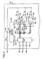
Figure 3 , a reducedsize heater chip 25 of the present invention has anintegral voltage regulator 330. An input terminal, such as abond pad 281, supplies the heater chip with a single input voltage, preferably +10.8 volts. Aninput voltage line 332 connects to the input terminal to provide an electrical path for the input voltage to be supplied to the voltage regulator atnode 331. During use, the voltage regulator derives at least two output voltages, supplied atnodes voltage signal line 336 and about +7.5 volts on outputvoltage signal line 338.Figure 5 , described below, shows one embodiment of a voltage regulator for use with this invention. - A
control logic circuit 340 receives logic inputs from inputterminal bond pads drivers 350 that activate, or not, switches 360. As shown, the switches embody power FETs having a gate coupled to an output of thedriver 350, a source coupled to a ground path resistor RG, and a drain coupled to a resistive heater element RH that acts to heat and eject ink through nozzle orifices (dashed lines) upon activation of the switch to which they are coupled. Because other resistance may exist in the path between the input terminal and the resistive heater elements RH, an additional resistance is shown electrically there between as RL. - In a preferred embodiment, the outputs 342 of the control logic circuit include a primitive, an address and an extended address line for addressing
particular drivers 350 and a firing pulse line. In other embodiments, these lines may include more, fewer or other signals. - Regarding voltage powering of the
control logic circuit 340, thedrivers 350 and the resistive heater elements RH, the first and secondoutput voltage lines voltage regulator 330 supply voltages to the control logic circuit and the drivers, respectively, while the input voltage frominput terminal 281 supplies voltage to the resistive heaters. In this manner, the control logic circuit can receive one voltage for CMOS-based logic devices and the drivers can simultaneously receive another voltage while only one voltage is supplied to the heater chip. In a preferred embodiment, the voltage online 336 is about +3.3 volts while the voltage online 338 is about +7.5 volts. Thereafter, when an output of anyindividual driver 350 activates its corresponding FET, a Vgs (gate to source voltage) of the FET can become as large as about +7.5 volts. - With reference to the following Table, skilled artisans will notice that the resistance (RFET) of a 400 micron wide FET area with a Vgs of about +7.5 volts equates to the same resistance of a
prior art 500 micron wide FET area with a Vgs of about +5 volts.Table: Measured Characteristics of 400 and 500 micron wide FET areas and 42 micron FET area length at Room Temperature and 320mA Rated Current Vgs (Volts) RFET (Ω) FET Area Width (microns) 3.3 7.0 500 5 4.5 500 7.5 4.0 500 3.3 8.0 400 5 4.9 400 7.5 4.5 400 - Accordingly, with reference to
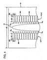
Figure 4 , since a FET width d2 can decrease with an increase in Vgs and still maintain a drain current suitable for firing ink from a resistive heater element, the overall width d3 of the heater chip can correspondingly decrease. This saves silicon costs. As representation of silicon savings, one actual wafer production of a plurality of heater chips having the above decrease in FET width corresponded to about a six percent increase in dies-per-wafer from 199 to 212. - Since the heater chip shown embodies a single via 32 with left and right rows of FETs each narrowing from 500 to 400 microns, the distance d3 of the heater chip can correspondingly narrow by about 200 microns. Even further, if the heater chip has multiple vias and multiple left and/or right rows of power FETs, the width of the heater chip can narrow by even more distance.
- As still other evidence of improvement over the prior art, since the input terminals of the heater chip now only need one input voltage, the
TAB circuit 20 can have a corresponding decrease in conductors and/or I/O connectors and the printer need only provide for a single instance of input voltage. - Regarding the distance d1 between adjacent ones of FETs, this value preferably corresponds to the vertical pitch distance between resistive heater elements. As such, since pitch typically corresponds to printer resolution in dots-per-inch (DPI), the invention contemplates distances of 1/600th of an
inch 1/300th, 1/1200th, 1/2400th or other. - With reference to
Figure 5 , one embodiment of an integral or on-chip voltage regulator 330 includes three sub-circuits, especially avoltage reference circuit 500 and first andsecond regulator circuits - In general, the
voltage reference circuit 500 comprises a voltage divider consisting of a pair of resistors R6, R7 in series. The ratio of the two resistors is selected to achieve a desired reference voltage at anode 1 between them. In a preferred embodiment, R6 is a 150 K ohm resistor, R7 is a 66 K ohm resistor and since the input voltage is about 10.8 volts, a reference voltage of about 3.3 volts is achieved. Additionally, a capacitor C3 may be provided to assist in stabilizing the voltage. One preferred C3 value is 200 pF. - Regarding the
regulator circuit 510, it comprises an op-amp 512 with its inverting input (-) connected to thereference voltage node 1. The non-inverting input (+) connects to a drain of apmos transistor 514. During use, the pmos transistor acts as a pass device between the input voltage atnode 331 and the output voltage atnode 333. By setting the feedback resistor R2 to some large value (100K ohms in one embodiment) and having no resistance in the path between the non-inverting input (-) of the op-amp andnode 333, the op-amp 4 becomes configured for a unity gain. As such, in this configuration the op-amp will vary the voltage at the output of op-amp 512 in order to hold the voltage atnode 333 to be the same value as the inverting input (-), namely 3.3 volts. Resistor R1 (13.2 k ohms in one embodiment) is used to force a constant 250 A of current through thepass device 514 to aid stability. The capacitance C1 (preferably 2 nF) at theoutput node 333 of theregulator circuit 510 provides additional circuit stability. - The
regulator circuit 520 is similar toregulator circuit 510 except that a resistor R4 (125 K ohm) is added between the non-inverting input (-) of the op-amp 522 and a drain of thepass device 524. In turn, amplifier gain increases such that an output of the op-amp 522 attempts to hold the voltage atnode 335 at a constant 7.5 volts. The value of the loading resistor R5 (30 K ohm) has also been modified to provide the same constant 250 A of current flow. - As shown with reference to
Figure 6 , to ensure relatively smooth voltage waveforms on the heater chip, pluralities of capacitors C become placed in electric parallel with the input voltage Vin online 332 and the output voltages V1, V2, onlines heater chip 25 for each of the input Vin and output voltages V1, V2 and are dispersed about an entirety of the heater chip. - Appreciating that the heater chip comprises a plurality of thin film layers on a semiconductor substrate, with reference to
Figures 7A and 7B , two embodiments of capacitors C are shown. In both embodiments, agate oxide layer 702 and apolysilicon layer 704 overlie asubstrate 700. The positive capacitor electrode attaches to the polysilicon layer while the negative capacitor electrode attaches to an electrically grounded substrate. InFigure 7A , an n-well region 706 of dopant underlies the gate oxide and is tied electrically to the grounded substrate. Appreciating the substrate is preferably a p-type, 100 orientation wafer, preferred embodiments of dopants include phosphorous and arsenic. Preferred thickness of the gate oxide is about 185 angstroms +/- about 15% and polysilicon layer is about 4500 angstroms +/- about 10%. - Those skilled in the art will appreciate that the structures depicted in
Figures 7A and 7B , show the results of a substrate having been processed through a series of growth, deposition, masking, photolithography, and/or etching or other processing steps. As such, preferred deposition techniques include, but are not limited to, any variety of chemical vapor depositions (CVD), physical vapor depositions (PVD), epitaxy, evaporation, sputtering or other similarly known techniques. Preferred CVD techniques include low pressure (LP) ones, but could also include atmospheric pressure (AP), plasma enhanced (PE), high density plasma (HDP) or other. Preferred etching techniques include, but are not limited to, any variety of wet or dry etches, reactive ion etches, deep reactive ion etches, etc. Preferred photolithography steps include, but are not limited to, exposure to ultraviolet or x-ray light sources, or other, and photomasking includes photomasking islands and/or photomasking holes. The particular embodiment, island or hole, depends upon whether the configuration of the mask is a clear-field or dark-field mask as those terms are well understood in the art. - In a preferred embodiment, the
substrate 700 includes a silicon wafer of p-type, 100 orientation, wafer having a resistivity of 5-20 ohm/cm. Its beginning thickness is preferably any one of 525 +/- 20 microns M1.5-89, 625 +/- 20 microns M1.7-89, or 625 +/- 15 microns M1.13-90 with respective wafer diameters of 100 +/- 0.50 mm, 125 +/-0.50 mm, and 150 +/- 0.50 mm. - Finally, the foregoing description is presented for purposes of illustration and description of the various aspects of the invention. The descriptions are not intended, however, to be exhaustive or to limit the invention to the precise form disclosed. For example, the input and output voltages of the voltage regulator could be any value other than those 10, 10.8, 3.3 and 7.5 volt values described. The switch could be any switch other than a transistor or a transistor, such as npn, pnp, bi-polar transistor, n-channel, p-channel or dual channel JFET, MOSFET, IGFET, or other, instead of just the power FETs shown. The input terminals of the heater chip could comprise wires, bumps, or other instead of the bond pads shown. The drivers could embody a logic NAND with an inverter, or other, as opposed to the AND 350 shown. The
inkjet printhead 10 could embody a side-shooter instead of a top-shooter. The resistive heaters could embody piezoelectric or other transducers.
Claims (9)
- A heater chip (25) for an inkjet printhead (10), comprising:an input terminal (28) for receiving an input voltage;a voltage regulator (330) coupled to said input terminal having a first (336) and second (338) output voltage line with voltages thereon during use derived from said input voltage;a driver (350) coupled to one of said first (336) and second (338) output voltage lines for receiving powering voltage;a control logic circuit (340) coupled to said driver and to the other of said first (336) and second (338) output voltage lines for receiving power voltage;a transistor coupled to said driver; anda resistive heater element coupled to said transistor and to said input terminal for receiving powering voltage from said input voltage.
- The heater chip (25) of claim 1, wherein during use one of said first and second output voltage lines is about 3.3 volts while the other of said first and second output voltage lines is about 7.5 volts.
- The heater chip (25) of claim 1, wherein during use said input voltage is about 10.8 volts.
- The heater chip (25) of claim 1, wherein said input terminal is a bond pad (28).
- The heater chip (25) of claim 1, wherein an area width of said transistor is about 400 microns.
- A method of operating a heater chip (25) of an inkjet printhead (10), comprising:supplying an input voltage to a voltage regulator (330);deriving at least a first (336) and second (338) output voltage from said input voltage, said deriving being done by said voltage regulator (330);supplying one of said first and second output voltage to a driver (350);activating a switch coupled to said driver (350) by an output of said driver; andsupplying said input voltage to a resistive heater clement coupled to an output of said switch;further including supplying the other of said first and second output voltage to a control logic circuit (340) having an output coupled to said driver.
- The method of claim 6, wherein the switch is a FET and wherein the activating the switch further includes supplying said output of said driver such that a Vgs of the FET is about 7.5 volts.
- The method of claim 6, wherein the deriving the at least first and second output voltage further includes generating a first voltage of about 3.3 volts and a second voltage of about 7.5 volts.
- The method of claim 6, wherein the supplying the input voltage further includes supplying a voltage of about 10.8 volts from an inkjet printer.
Applications Claiming Priority (3)
| Application Number | Priority Date | Filing Date | Title |
|---|---|---|---|
| US331001 | 2002-12-27 | ||
| US10/331,001 US6789871B2 (en) | 2002-12-27 | 2002-12-27 | Reduced size inkjet printhead heater chip having integral voltage regulator and regulating capacitors |
| PCT/US2003/041272 WO2004060677A2 (en) | 2002-12-27 | 2003-12-24 | Reduced size inkjet printhead heater chip having integral voltage regulator and regulating capacitors |
Publications (3)
| Publication Number | Publication Date |
|---|---|
| EP1587684A2 EP1587684A2 (en) | 2005-10-26 |
| EP1587684A4 EP1587684A4 (en) | 2008-10-29 |
| EP1587684B1 true EP1587684B1 (en) | 2012-02-29 |
Family
ID=32654637
Family Applications (1)
| Application Number | Title | Priority Date | Filing Date |
|---|---|---|---|
| EP03800175A Expired - Lifetime EP1587684B1 (en) | 2002-12-27 | 2003-12-24 | Reduced size inkjet printhead heater chip having integral voltage regulator and regulating capacitors |
Country Status (6)
| Country | Link |
|---|---|
| US (1) | US6789871B2 (en) |
| EP (1) | EP1587684B1 (en) |
| CN (1) | CN100358720C (en) |
| AU (1) | AU2003299902A1 (en) |
| TW (1) | TWI330594B (en) |
| WO (1) | WO2004060677A2 (en) |
Families Citing this family (28)
| Publication number | Priority date | Publication date | Assignee | Title |
|---|---|---|---|---|
| US20050111151A1 (en) * | 2003-11-25 | 2005-05-26 | Lam Don T. | Isolation circuit for a communication system |
| GB0419451D0 (en) * | 2004-09-02 | 2004-10-06 | Koninkl Philips Electronics Nv | Inkjet print head |
| US20060221140A1 (en) * | 2005-04-01 | 2006-10-05 | Lexmark International, Inc. | Low profile printhead |
| US20060226139A1 (en) * | 2005-04-06 | 2006-10-12 | Craig Jennings | Wok-piece positioner |
| US7673957B2 (en) * | 2005-05-04 | 2010-03-09 | Lexmark International, Inc. | Method for determining an optimal non-nucleating heater pulse for use with an ink jet printhead |
| US7722185B2 (en) | 2005-12-05 | 2010-05-25 | Silverbrook Research Pty Ltd | Cradle for printhead cartridge having power storage interface |
| JP5200360B2 (en) * | 2006-09-29 | 2013-06-05 | 富士ゼロックス株式会社 | Exposure apparatus and image forming apparatus |
| US7806495B2 (en) * | 2006-12-05 | 2010-10-05 | Canon Kabushiki Kaisha | Head substrate, printhead, head cartridge, and printing apparatus |
| JP2009119714A (en) * | 2007-11-14 | 2009-06-04 | Canon Inc | Recording head and recording apparatus |
| US8172369B2 (en) * | 2008-12-30 | 2012-05-08 | Lexmark International, Inc. | Inkjet printhead substrate with distributed heater elements |
| JP5723137B2 (en) * | 2009-11-26 | 2015-05-27 | キヤノン株式会社 | Printhead substrate, printhead, and printing apparatus |
| CN102689513B (en) * | 2011-03-23 | 2015-02-18 | 研能科技股份有限公司 | Inkjet head structure |
| EP3326823B1 (en) | 2011-10-14 | 2020-12-09 | Hewlett-Packard Development Company, L.P. | Firing actuator power supply system |
| CN102423967A (en) * | 2011-10-25 | 2012-04-25 | 珠海天威技术开发有限公司 | Consumable chip and consumable container |
| JP2014076567A (en) * | 2012-10-10 | 2014-05-01 | Seiko Epson Corp | Liquid jet device |
| JP6222998B2 (en) * | 2013-05-31 | 2017-11-01 | キヤノン株式会社 | Element substrate, full line recording head, and recording apparatus |
| JP6376829B2 (en) * | 2014-05-09 | 2018-08-22 | キヤノン株式会社 | Liquid ejection substrate, liquid ejection head, and recording apparatus |
| US9833991B2 (en) * | 2014-09-29 | 2017-12-05 | Funai Electric Co., Ltd. | Printhead and an inkjet printer |
| JP6519417B2 (en) * | 2014-10-07 | 2019-05-29 | 株式会社デンソー | Semiconductor device and method of manufacturing the same |
| EP3212426B1 (en) * | 2014-10-27 | 2021-05-26 | Hewlett-Packard Development Company, L.P. | Printing device |
| WO2017131614A1 (en) * | 2016-01-25 | 2017-08-03 | Hewlett-Packard Development Company, L.P. | Fluid device |
| JP6716997B2 (en) * | 2016-03-30 | 2020-07-01 | 株式会社ジェイテクト | Control device and method for controlling fluid supply device |
| EP3856522B1 (en) * | 2018-09-24 | 2024-02-21 | Hewlett-Packard Development Company, L.P. | A fluidic die and a process for a fluidic die |
| WO2020145970A1 (en) * | 2019-01-09 | 2020-07-16 | Hewlett-Packard Development Company, L.P. | Printhead voltage regulators |
| KR102621225B1 (en) * | 2019-02-06 | 2024-01-04 | 휴렛-팩커드 디벨롭먼트 컴퍼니, 엘.피. | Die for printhead |
| CN113365841B (en) | 2019-02-06 | 2022-10-04 | 惠普发展公司,有限责任合伙企业 | Die for printhead |
| US11433664B2 (en) | 2019-02-06 | 2022-09-06 | Hewlett-Packard Development Company, L.P. | Writing a nonvolatile memory to programmed levels |
| MX2021009131A (en) | 2019-02-06 | 2021-09-08 | Hewlett Packard Development Co | Die for a printhead. |
Family Cites Families (20)
| Publication number | Priority date | Publication date | Assignee | Title |
|---|---|---|---|---|
| JPH0785937B2 (en) | 1986-09-12 | 1995-09-20 | 三菱電機株式会社 | Driver IC and recording head |
| US5300968A (en) | 1992-09-10 | 1994-04-05 | Xerox Corporation | Apparatus for stabilizing thermal ink jet printer spot size |
| US5371530A (en) | 1993-05-04 | 1994-12-06 | Xerox Corporation | Thermal ink jet printhead having a switched stand-by mode |
| JPH08224879A (en) | 1994-12-19 | 1996-09-03 | Xerox Corp | Method for adjusting threshold of liquid drop ejector |
| US5517053A (en) | 1995-01-09 | 1996-05-14 | Northrop Grumman Corporation | Self stabilizing heater controlled oscillating transistor |
| US5850242A (en) | 1995-03-07 | 1998-12-15 | Canon Kabushiki Kaisha | Recording head and recording apparatus and method of manufacturing same |
| US5734392A (en) | 1995-09-14 | 1998-03-31 | Lexmark International, Inc. | Ink jet printhead heating during margin periods |
| US5757394A (en) * | 1995-09-27 | 1998-05-26 | Lexmark International, Inc. | Ink jet print head identification circuit with programmed transistor array |
| US5933161A (en) | 1996-03-21 | 1999-08-03 | Fuji Xerox Co., Ltd. | Ink-jet recorder having a driving circuit for driving heat-generating elements |
| US5736997A (en) | 1996-04-29 | 1998-04-07 | Lexmark International, Inc. | Thermal ink jet printhead driver overcurrent protection scheme |
| DE69733295T2 (en) | 1996-06-26 | 2006-02-02 | Canon K.K. | Recording head and recording apparatus using the same |
| US6081280A (en) | 1996-07-11 | 2000-06-27 | Lexmark International, Inc. | Method and apparatus for inhibiting electrically induced ink build-up on flexible, integrated circuit connecting leads, for thermal ink jet printer heads |
| US6234612B1 (en) | 1997-03-25 | 2001-05-22 | Lexmark International, Inc. | Ink jet printing apparatus having first and second print cartridges receiving energy pulses from a common drive circuit |
| US6439680B1 (en) | 1999-06-14 | 2002-08-27 | Canon Kabushiki Kaisha | Recording head, substrate for use of recording head, and recording apparatus |
| US6499821B1 (en) * | 1999-07-22 | 2002-12-31 | Canon Kabushiki Kaisha | Ink jet printing apparatus and printing head |
| JP4585660B2 (en) * | 1999-07-22 | 2010-11-24 | キヤノン株式会社 | Inkjet printing apparatus and inkjet printing method |
| US6409298B1 (en) | 2000-05-31 | 2002-06-25 | Lexmark International, Inc. | System and method for controlling current density in thermal printheads |
| US6431677B1 (en) | 2000-06-08 | 2002-08-13 | Lexmark International, Inc | Print head drive scheme |
| US6616268B2 (en) * | 2001-04-12 | 2003-09-09 | Lexmark International, Inc. | Power distribution architecture for inkjet heater chip |
| JP2002355970A (en) * | 2001-05-31 | 2002-12-10 | Canon Inc | Recording device |
-
2002
- 2002-12-27 US US10/331,001 patent/US6789871B2/en not_active Expired - Lifetime
-
2003
- 2003-12-24 WO PCT/US2003/041272 patent/WO2004060677A2/en not_active Ceased
- 2003-12-24 AU AU2003299902A patent/AU2003299902A1/en not_active Abandoned
- 2003-12-24 CN CNB2003801090289A patent/CN100358720C/en not_active Expired - Lifetime
- 2003-12-24 EP EP03800175A patent/EP1587684B1/en not_active Expired - Lifetime
- 2003-12-26 TW TW092137139A patent/TWI330594B/en not_active IP Right Cessation
Also Published As
| Publication number | Publication date |
|---|---|
| WO2004060677A2 (en) | 2004-07-22 |
| US20040125157A1 (en) | 2004-07-01 |
| WO2004060677A3 (en) | 2005-05-19 |
| US6789871B2 (en) | 2004-09-14 |
| AU2003299902A8 (en) | 2004-07-29 |
| EP1587684A2 (en) | 2005-10-26 |
| TW200508035A (en) | 2005-03-01 |
| EP1587684A4 (en) | 2008-10-29 |
| AU2003299902A1 (en) | 2004-07-29 |
| CN1738715A (en) | 2006-02-22 |
| CN100358720C (en) | 2008-01-02 |
| HK1088284A1 (en) | 2006-11-03 |
| TWI330594B (en) | 2010-09-21 |
Similar Documents
| Publication | Publication Date | Title |
|---|---|---|
| EP1587684B1 (en) | Reduced size inkjet printhead heater chip having integral voltage regulator and regulating capacitors | |
| EP1314562B1 (en) | Inkjet printhead assembly having very high drop rate generation | |
| US7984956B2 (en) | Liquid jet apparatus and printing apparatus | |
| JP4041914B2 (en) | Two drop size print head | |
| JP3404470B2 (en) | Inkjet print head | |
| JP5025345B2 (en) | Inkjet recording head and inkjet recording apparatus | |
| US7445316B2 (en) | Printhead substrate, printhead, head cartridge, and printing apparatus | |
| EP0532877A2 (en) | Recording apparatus, recording head and substrate therefor | |
| CN101765506B (en) | Printheads | |
| TW581730B (en) | Narrow multi-color ink jet printhead | |
| TW542792B (en) | Narrow ink jet printhead | |
| US9802404B2 (en) | Chip layout to enable multiple heater chip vertical resolutions | |
| CN1083338C (en) | Printhead driver for jetting heaters and substrate heater in ink jet printer and method of controlling such heaters | |
| US6764163B2 (en) | Heater configuration for tri-color heater chip | |
| US7354139B2 (en) | Printhead substrate, printhead, head cartridge, and printing apparatus | |
| EP3186085B1 (en) | Printhead and inkjet printer | |
| HK1088284B (en) | Heater chip and method of operating the same, printhead, printer | |
| EP1694508B1 (en) | Microfluid ejection device having efficient logic and driver circuitry | |
| US10960666B2 (en) | Element substrate, liquid discharge head, and printing apparatus | |
| US9278518B2 (en) | Printhead substrate, printhead, and printing apparatus | |
| KR20060095492A (en) | Liquid ejection head, liquid ejection apparatus, liquid ejection method, and ejection medium of liquid ejection head | |
| JP2002187270A (en) | Ink jet recording device | |
| JP2004050492A (en) | Inkjet head drive circuit | |
| JPH1095116A (en) | Ink jet recording head, ink jet recording apparatus and ink jet recording method | |
| JPH0952362A (en) | Ink jet recording apparatus |
Legal Events
| Date | Code | Title | Description |
|---|---|---|---|
| PUAI | Public reference made under article 153(3) epc to a published international application that has entered the european phase |
Free format text: ORIGINAL CODE: 0009012 |
|
| 17P | Request for examination filed |
Effective date: 20050727 |
|
| AK | Designated contracting states |
Kind code of ref document: A2 Designated state(s): AT BE BG CH CY CZ DE DK EE ES FI FR GB GR HU IE IT LI LU MC NL PT RO SE SI SK TR |
|
| AX | Request for extension of the european patent |
Extension state: AL LT LV MK |
|
| DAX | Request for extension of the european patent (deleted) | ||
| RBV | Designated contracting states (corrected) |
Designated state(s): DE FR GB |
|
| A4 | Supplementary search report drawn up and despatched |
Effective date: 20080926 |
|
| 17Q | First examination report despatched |
Effective date: 20090914 |
|
| GRAP | Despatch of communication of intention to grant a patent |
Free format text: ORIGINAL CODE: EPIDOSNIGR1 |
|
| GRAS | Grant fee paid |
Free format text: ORIGINAL CODE: EPIDOSNIGR3 |
|
| GRAA | (expected) grant |
Free format text: ORIGINAL CODE: 0009210 |
|
| AK | Designated contracting states |
Kind code of ref document: B1 Designated state(s): DE FR GB |
|
| REG | Reference to a national code |
Ref country code: GB Ref legal event code: FG4D |
|
| REG | Reference to a national code |
Ref country code: DE Ref legal event code: R096 Ref document number: 60340162 Country of ref document: DE Effective date: 20120426 |
|
| PLBE | No opposition filed within time limit |
Free format text: ORIGINAL CODE: 0009261 |
|
| STAA | Information on the status of an ep patent application or granted ep patent |
Free format text: STATUS: NO OPPOSITION FILED WITHIN TIME LIMIT |
|
| 26N | No opposition filed |
Effective date: 20121130 |
|
| REG | Reference to a national code |
Ref country code: DE Ref legal event code: R097 Ref document number: 60340162 Country of ref document: DE Effective date: 20121130 |
|
| REG | Reference to a national code |
Ref country code: GB Ref legal event code: 732E Free format text: REGISTERED BETWEEN 20131107 AND 20131113 |
|
| REG | Reference to a national code |
Ref country code: DE Ref legal event code: R081 Ref document number: 60340162 Country of ref document: DE Owner name: FUNAI ELECTRIC CO., LTD, JP Free format text: FORMER OWNER: LEXMARK INTERNATIONAL, INC., LEXINGTON, US Effective date: 20131107 Ref country code: DE Ref legal event code: R081 Ref document number: 60340162 Country of ref document: DE Owner name: FUNAI ELECTRIC CO., LTD, JP Free format text: FORMER OWNER: LEXMARK INTERNATIONAL, INC., LEXINGTON, US Effective date: 20120306 Ref country code: DE Ref legal event code: R082 Ref document number: 60340162 Country of ref document: DE Representative=s name: DEHNS, GB Effective date: 20131107 Ref country code: DE Ref legal event code: R081 Ref document number: 60340162 Country of ref document: DE Owner name: FUNAI ELECTRIC CO., LTD, DAITO CITY, JP Free format text: FORMER OWNER: LEXMARK INTERNATIONAL, INC., LEXINGTON, KY., US Effective date: 20120306 Ref country code: DE Ref legal event code: R081 Ref document number: 60340162 Country of ref document: DE Owner name: FUNAI ELECTRIC CO., LTD, DAITO CITY, JP Free format text: FORMER OWNER: LEXMARK INTERNATIONAL, INC., LEXINGTON, KY., US Effective date: 20131107 |
|
| REG | Reference to a national code |
Ref country code: FR Ref legal event code: TP Owner name: FUNAI ELECTRIC CO LTD, JP Effective date: 20140102 |
|
| REG | Reference to a national code |
Ref country code: FR Ref legal event code: PLFP Year of fee payment: 13 |
|
| PGFP | Annual fee paid to national office [announced via postgrant information from national office to epo] |
Ref country code: GB Payment date: 20151223 Year of fee payment: 13 |
|
| PGFP | Annual fee paid to national office [announced via postgrant information from national office to epo] |
Ref country code: FR Payment date: 20151110 Year of fee payment: 13 |
|
| REG | Reference to a national code |
Ref country code: DE Ref legal event code: R084 Ref document number: 60340162 Country of ref document: DE |
|
| GBPC | Gb: european patent ceased through non-payment of renewal fee |
Effective date: 20161224 |
|
| REG | Reference to a national code |
Ref country code: FR Ref legal event code: ST Effective date: 20170831 |
|
| PG25 | Lapsed in a contracting state [announced via postgrant information from national office to epo] |
Ref country code: FR Free format text: LAPSE BECAUSE OF NON-PAYMENT OF DUE FEES Effective date: 20170102 |
|
| PG25 | Lapsed in a contracting state [announced via postgrant information from national office to epo] |
Ref country code: GB Free format text: LAPSE BECAUSE OF NON-PAYMENT OF DUE FEES Effective date: 20161224 |
|
| REG | Reference to a national code |
Ref country code: DE Ref legal event code: R082 Ref document number: 60340162 Country of ref document: DE |
|
| PGFP | Annual fee paid to national office [announced via postgrant information from national office to epo] |
Ref country code: DE Payment date: 20220622 Year of fee payment: 20 |
|
| REG | Reference to a national code |
Ref country code: DE Ref legal event code: R071 Ref document number: 60340162 Country of ref document: DE |