EP1586857B1 - An optical device that measures distance between the device and a surface - Google Patents
An optical device that measures distance between the device and a surface Download PDFInfo
- Publication number
- EP1586857B1 EP1586857B1 EP04026868A EP04026868A EP1586857B1 EP 1586857 B1 EP1586857 B1 EP 1586857B1 EP 04026868 A EP04026868 A EP 04026868A EP 04026868 A EP04026868 A EP 04026868A EP 1586857 B1 EP1586857 B1 EP 1586857B1
- Authority
- EP
- European Patent Office
- Prior art keywords
- light
- optical device
- speckle pattern
- wavelength
- distance
- Prior art date
- Legal status (The legal status is an assumption and is not a legal conclusion. Google has not performed a legal analysis and makes no representation as to the accuracy of the status listed.)
- Ceased
Links
Images


Classifications
-
- G—PHYSICS
- G01—MEASURING; TESTING
- G01D—MEASURING NOT SPECIALLY ADAPTED FOR A SPECIFIC VARIABLE; ARRANGEMENTS FOR MEASURING TWO OR MORE VARIABLES NOT COVERED IN A SINGLE OTHER SUBCLASS; TARIFF METERING APPARATUS; MEASURING OR TESTING NOT OTHERWISE PROVIDED FOR
- G01D5/00—Mechanical means for transferring the output of a sensing member; Means for converting the output of a sensing member to another variable where the form or nature of the sensing member does not constrain the means for converting; Transducers not specially adapted for a specific variable
- G01D5/26—Mechanical means for transferring the output of a sensing member; Means for converting the output of a sensing member to another variable where the form or nature of the sensing member does not constrain the means for converting; Transducers not specially adapted for a specific variable characterised by optical transfer means, i.e. using infrared, visible, or ultraviolet light
- G01D5/28—Mechanical means for transferring the output of a sensing member; Means for converting the output of a sensing member to another variable where the form or nature of the sensing member does not constrain the means for converting; Transducers not specially adapted for a specific variable characterised by optical transfer means, i.e. using infrared, visible, or ultraviolet light with deflection of beams of light, e.g. for direct optical indication
- G01D5/30—Mechanical means for transferring the output of a sensing member; Means for converting the output of a sensing member to another variable where the form or nature of the sensing member does not constrain the means for converting; Transducers not specially adapted for a specific variable characterised by optical transfer means, i.e. using infrared, visible, or ultraviolet light with deflection of beams of light, e.g. for direct optical indication the beams of light being detected by photocells
-
- G—PHYSICS
- G06—COMPUTING OR CALCULATING; COUNTING
- G06F—ELECTRIC DIGITAL DATA PROCESSING
- G06F3/00—Input arrangements for transferring data to be processed into a form capable of being handled by the computer; Output arrangements for transferring data from processing unit to output unit, e.g. interface arrangements
- G06F3/01—Input arrangements or combined input and output arrangements for interaction between user and computer
- G06F3/03—Arrangements for converting the position or the displacement of a member into a coded form
- G06F3/0304—Detection arrangements using opto-electronic means
- G06F3/0317—Detection arrangements using opto-electronic means in co-operation with a patterned surface, e.g. absolute position or relative movement detection for an optical mouse or pen positioned with respect to a coded surface
-
- G—PHYSICS
- G06—COMPUTING OR CALCULATING; COUNTING
- G06F—ELECTRIC DIGITAL DATA PROCESSING
- G06F3/00—Input arrangements for transferring data to be processed into a form capable of being handled by the computer; Output arrangements for transferring data from processing unit to output unit, e.g. interface arrangements
- G06F3/01—Input arrangements or combined input and output arrangements for interaction between user and computer
- G06F3/03—Arrangements for converting the position or the displacement of a member into a coded form
- G06F3/033—Pointing devices displaced or positioned by the user, e.g. mice, trackballs, pens or joysticks; Accessories therefor
- G06F3/0346—Pointing devices displaced or positioned by the user, e.g. mice, trackballs, pens or joysticks; Accessories therefor with detection of the device orientation or free movement in a three-dimensional [3D] space, e.g. 3D mice, 6-DOF [six degrees of freedom] pointers using gyroscopes, accelerometers or tilt-sensors
-
- G—PHYSICS
- G06—COMPUTING OR CALCULATING; COUNTING
- G06F—ELECTRIC DIGITAL DATA PROCESSING
- G06F3/00—Input arrangements for transferring data to be processed into a form capable of being handled by the computer; Output arrangements for transferring data from processing unit to output unit, e.g. interface arrangements
- G06F3/01—Input arrangements or combined input and output arrangements for interaction between user and computer
- G06F3/03—Arrangements for converting the position or the displacement of a member into a coded form
- G06F3/033—Pointing devices displaced or positioned by the user, e.g. mice, trackballs, pens or joysticks; Accessories therefor
- G06F3/0354—Pointing devices displaced or positioned by the user, e.g. mice, trackballs, pens or joysticks; Accessories therefor with detection of two-dimensional [2D] relative movements between the device, or an operating part thereof, and a plane or surface, e.g. 2D mice, trackballs, pens or pucks
- G06F3/03545—Pens or stylus
Definitions
- Optical navigation devices conventionally use a laser-generated light that reflects off a surface to a detector.
- the detector includes, for example, a complementary metal-oxide semiconductor (CMOS) imager array.
- CMOS complementary metal-oxide semiconductor
- the reflection of the light produces a pattern of speckle that is captured by the CMOS imager.
- CMOS imager As the device is moved relative to the surface (or vice versa), successive images are rapidly captured and compared to determine the amount of movement. The rate at which images are captured can be used to determine the velocity of movement.
- Optical navigation devices generally perform well for tracking two-dimensional movements. For example, an optical mouse very precisely tracks movement along the surface of a mouse pad. However, optical navigation can be problematic in certain applications that involve three-dimensional movements.
- the document US-B1-6 188 482 describes an optical device comprising a light source that emits light onto a surface and a detector that receives light reflected from the surface. The reflected light produces different speckle patterns at different distances between the detector of the optical device and the surface. A computer compares stored speckle pattern images to calculate resultant out-of-plane displacements.
- Embodiments in accordance with the invention pertain to an optical device and methods thereof.
- the device includes a first light source adapted to emit light onto a surface, and a detector adapted to receive light reflected from the surface.
- the reflected light produces a speckle pattern.
- the distance between the optical device and the surface can be measured using a quantifiable attribute associated with the speckle pattern.
- the detector can also track transverse movement relative to the surface.
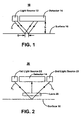
- Figure 1 is a block diagram showing elements of an optical device 10 in one embodiment in accordance with the invention.
- Optical device 10 can be an optical mouse or an optical pen that may be used with a computer system, for example.
- optical device 10 includes a light source 12 and a detector 14.
- Device 10 can include other elements in addition to those described or illustrated herein, such as but not limited to circuitry and other electronics associated with the light source 12 and the detector 14, processing capability for processing image data and for other processing functions, and storage capability for storing image data or images as well as other information.
- Detector 14 can utilize, for example, a charge-coupled device (CCD) imager array or a complementary metal-oxide semiconductor (CMOS) imager array.
- Light source 12 can utilize a coherent light source such as a laser.
- light source 12 can utilize a narrow-band light-emitting diode (LED) or an LED with an optical filter.
- LED narrow-band light-emitting diode
- light source 12 emits light at a fixed wavelength.
- light source 12 emits light over a range of wavelengths. In the latter embodiment, light source 12 has the capability of dynamically changing from one wavelength to another wavelength.
- surface 16 In operation, light from light source 12 is reflected from surface 16 to detector 14.
- Surface 16 can be virtually any kind of surface that can reflect light in this manner.
- Surface 16 may be, for example, a mouse pad or similar type of surface.
- Surface 16 may also be, for example, the display screen of a computer system.
- surface 16 is representative of virtually any surface except optically flat surfaces.
- light source 12 emits light having wavelength ⁇ (as mentioned above, the wavelength may be fixed or it may be changeable).
- the length of the spot on surface 16 that is illuminated by light source 12 is given by D.
- the distance between detector 14 and the surface 16 is given by h.
- the speckle pattern typically includes a number of individual speckles spatially distributed with a known statistical distribution.
- Various statistical measures can be calculated to describe the speckle pattern.
- a statistical measure commonly used is the average size of the speckles in the speckle pattern.
- Figure 2 is a block diagram showing elements of an optical device 20 in another embodiment in accordance with the invention.
- Optical device 20 can be an optical mouse or an optical pen that may be used with a computer system, for example.
- optical device 20 includes first light source 22, second light source 23, and detector 14.
- Device 20 can include other elements in addition to those described or illustrated herein.
- Detector 14 can utilize, for example, a CCD imager array or a CMOS imager array.
- Light sources 22 and 23 can each utilize a coherent light source such as a laser, a narrow-band LED, or an LED with an optical filter. In one embodiment, light sources 22 and 23 emit light at fixed wavelengths. In another embodiment, light sources 22 and 23 emit light over a range of wavelengths, with the capability of dynamically changing from one wavelength to another wavelength. In the example of Figure 2, light source 22 emits light having wavelength ⁇ 1 and light source 23 emits light having wavelength ⁇ 2 . The wavelengths ⁇ 1 and ⁇ 2 can be different from each other, or they can be the same, depending on how optical device 20 is used in operation.
- light from light sources 22 and 23 is directed to the same spot on surface 16 and reflected from surface 16 to detector 14.
- a lens 25 is used to direct the light reflected from surface 16 to detector 14.
- Figure 3 is a block diagram showing elements of an optical device 30 in yet another embodiment in accordance with the invention.
- Optical device 30 can be an optical mouse or an optical pen that may be used with a computer system, for example.
- optical device 30 includes first light source 32, second light source 34, first detector 31 and second detector 33.
- Device 30 can include other elements in addition to those described or illustrated herein.
- Detectors 31 and 33 can each utilize, for example, a CCD imager array or a CMOS imager array.
- Light sources 32 and 34 can each utilize a coherent light source such as a laser, a narrow-band LED, or an LED with an optical filter. In the example of Figure 3, light source 32 emits light having wavelength ⁇ 1 and light source 34 emits light having wavelength ⁇ 2 .
- light sources 32 and 34 emit light at fixed wavelengths. In another embodiment, light sources 32 and 34 emit light over a range of wavelengths, with the capability of dynamically changing from one wavelength to another wavelength. In either case, the wavelengths may be the same or different from each other, depending on how optical device 30 is used in operation. When different, the wavelengths used by light sources 32 and 34 may be close to each or far apart. Detectors 31 and 33 can use different technologies depending on the wavelengths used by light sources 32 and 34. In other words, one type of detector technology may be better suited to a particular wavelength than another. If, for example, the wavelengths are far apart, one type detector technology can be used with one wavelength and another type of detector technology can be used with the other wavelength.
- light from light sources 32 and 34 is directed to the same spot on surface 16.
- Light from light source 32 is reflected from surface 16 to detector 31, and light from light source 34 is reflected from surface 16 to detector 33.
- Figure 4 illustrates an optical device in operation in one embodiment in accordance with the invention.
- the optical device of Figure 4 can use either a single light source, as exemplified by optical device 10 of Figure 1, or multiple light sources, as exemplified by optical devices 20 and 30 of Figures 2 and 3.
- the multiple light sources emit light of the same or substantially the same wavelength.
- the term "substantially the same wavelength” is defined as follows.
- a change in the distance between the optical device and the surface 16 is identified by comparing a quantifiable attribute associated with the speckle pattern at a time T 1 with a quantifiable attribute associated with the speckle pattern at a time T 2 .
- the average speckle size at time T 1 is compared with the average speckle size at time T 2 (as discussed below, other quantifiable attributes other than average speckle size may be used).
- the average speckle size is influenced not only by the distance between the optical device and the surface, but by the wavelength of light.
- the wavelengths from different light sources need to be similar enough so that a change in average speckle size from one time to the next can be attributed to a change in distance and not to a difference in wavelength.
- the wavelengths from the different light sources would be identical. There is no distinct cutoff for an acceptable difference in wavelengths between multiple light sources; however, the closer the wavelengths of the two light sources are to each other, the better.
- detector 14 is a distance h 1 from surface 16.
- detector 14 is a distance h 2 from surface 16.
- the speckle patterns at times T 1 and T 2 will each include a number of speckles of different sizes, shapes and distributions.
- the speckle patterns at times T 1 and T 2 are each represented by a respective average transverse speckle size d 1 and d 2 .
- the average transverse speckle size d 1 at time T 1 is illustrated as element 42 in detector view 40.
- the average transverse speckle size d 2 at time T 2 is illustrated as element 44 in detector view 40.
- Equation (2) can be applied in a number of different ways.
- a change in distance is detected when there is a change in average transverse speckle size over time.
- a change in average speckle size over time e.g., over successive image frames
- the magnitude of a change in distance between the optical device (e.g., detector 14) and the surface 16, or the distance between the optical device and the surface can be determined. For example, with the optical device directly in contact with surface 16 at time T 1 , then d 1 is equal to d 2 and h 1 is equal to h 2 . Values of d 1 and h 1 can be retained in some manner. For example, they can be stored in a memory associated with the detector 14. At time T 2 , with the optical device moved to a distance h 2 , the average speckle size d 2 is determined. Using the values of h 1 , d 1 and d 2 in equation (2), a value for h 2 can be determined.
- the magnitude of the change from time T 1 to time T 2 (e.g., h 2 minus h 1 ) can be determined, or the actual distance to the surface at time T 2 (e.g., h 2 ) can be determined.
- the values of d 2 and h 2 can then be retained, and used in a manner similar to that just described to determine the distance or change in distance between the optical device and the surface at a later time (e.g., after the next time increment), and so on.
- Optical devices such as those described herein operate at frame rates of 1500 frames per second or more. Accordingly, the time difference between time T 1 and time T 2 can be very small. Also, imager arrays used in optical devices have very high resolutions that continue to improve. As such, relatively small changes in average speckle size can be measured, and therefore relatively small changes in distance can be detected.
- Figure 4 can be extended to optical devices 20 and 30 of Figures 2 and 3, respectively.
- optical device 20 which includes two light sources 22 and 23 and a single detector 14
- Figure 5 illustrates an optical device in operation in another embodiment in accordance with the invention.
- the optical device of Figure 5 can use either a single light source as exemplified by light source 12 of optical device 10 (Figure 1), or multiple light sources as exemplified by light sources 22 and 23 of optical device 20 ( Figure 2) and light sources 32 and 34 of Figure 3.
- the light source 12 of Figure 1 emits light having a wavelength ⁇ 1
- the light source 12 emits light having a wavelength ⁇ 2
- the wavelength of the light from light source 12 is allowed to dynamically change as the optical device is moved toward or away from the surface 16.
- the wavelength is automatically adjusted so that the average speckle size d 2 at time T 2 is the same (or approximately the same) as the average speckle size d 1 at time T 1 .
- one of the light sources is used at time T 1 and the other light source is used at time T 2 .
- the term "essentially constant" when applied to wavelengths is defined as follows.
- the wavelength of one light source is not adjusted; however, there may be some variance in wavelength due to fluctuations normally associated with the operation of the light source. For example, slight fluctuations in power may result in variations in wavelength. Note that a situation in which the variation in wavelength is other than "essentially constant" is covered by the alternate embodiment in which both wavelengths are adjusted.
- detector 14 is a distance h 1 from surface 16.
- detector 14 is a distance h 2 from surface 16.
- the wavelength of light source 12 is adjusted so that a relatively constant average speckle size is maintained over time (e.g., from time T 1 to time T 2 and at each subsequent time).
- the average transverse speckle size d 1 at time T 1 is illustrated as element 52 in detector view 50, and the average transverse speckle size d 2 time T 2 is illustrated as element 54 in detector view 50.
- the speckle patterns at times T 1 and T 2 will each include a number of speckles of different sizes, shapes and distributions.
- the term "essentially constant" when applied to average transverse speckle size is defined as follows.
- a change in the distance between the optical device and the surface 16 is identified by ratioing the wavelength of light source 12 at time T 1 and the wavelength of light source 12 at time T 2 .
- the degree to which a constant average transverse speckle size can be maintained has an influence on how accurately a change in distance can be measured.
- the average transverse speckle sizes at times T 1 and T 2 need to be similar enough so that a change in wavelength from one time to the next can be attributed to a change in distance and not to a difference in average transverse speckle size.
- the average transverse speckle size at times T 1 and T 2 would be identical. There is no distinct cutoff for an acceptable difference in average transverse speckle size at times T 1 and T 2 ; however, the closer the average transverse speckle size at times T 1 and T 2 are to each other, the better.
- Equation (3) can be applied in a number of different ways.
- a change in distance is detected when there is a change in wavelength over time.
- Wavelengths can be determined from the wavelength tuning characteristics of the light source(s).
- the magnitude of a change in distance between the optical device (e.g., detector 14) and the surface 16, or the distance between the optical device and the surface can be determined.
- ⁇ 1 is equal to ⁇ 2
- h 1 is equal to h 2 .
- Values of ⁇ 1 and h 1 can be retained in some manner. For example, they can be stored in a memory associated with the detector.
- the wavelength is adjusted to a second value ( ⁇ 2 ). The second value is selected so that the average speckle size remains the constant or essentially constant over time.
- a value for h 2 can be determined.
- the magnitude of the change from T 1 to T 2 e.g., h 2 minus h 1
- T 2 the actual distance to the surface at time T 2 (e.g., h 2 )
- the values of ⁇ 2 and h 2 can then be retained, and used in a manner similar to that just described to determine the distance or change in distance between the optical device and the surface at a later time (e.g., after the next time increment), and so on.
- the example of Figure 5 describes an application in which the wavelength is changed from ⁇ 1 to ⁇ 2 over time using a single light source.
- the example of Figure 5 can be extended to optical devices 20 and 30 of Figures 2 and 3, respectively, which each utilize two light sources. With two light sources, the wavelength at one of the light sources (e.g., ⁇ 1 ) can be held at a constant or nearly constant value, while the wavelength of the second light source (e.g., ⁇ 2 ) is adjusted in a manner that achieves a constant or essentially constant average transverse speckle size over time.
- the ratio of ⁇ 1 and ⁇ 2 alone with h 1 , can be used as described above to determine h 2 .
- the wavelength of the first light source can be held constant while the wavelength of the second light source is adjusted, and then from time T 2 to the next measurement (e.g., at time T 3 ), these roles can be reversed (with the wavelength of the second light source held constant while the wavelength of the first light source is adjusted). It is also possible that, with two light sources and suitable processing, both wavelengths can be adjusted over time.
- optical device 30 which includes two detectors 31 and 33, one detector can be used to collect a speckle pattern at time T 1 and the other detector can be used to collect a speckle pattern at time T 2 .
- Figure 6 illustrates an optical device in operation in yet another embodiment in accordance with the invention.
- the optical device of Figure 6 utilizes two light sources and two detectors as exemplified by optical device 30 of Figure 3.
- the wavelengths associated with the two light sources are different from each other.
- Both detectors 31 and 33 are at a distance h from surface 16.
- both light sources 32 and 34 illuminate the same spot on surface 16 (note that this is in contrast to the examples of Figures 4 and 5, in which consecutive measurements are made at times T 1 and T 2 ).
- Light source 32 emits light at a wavelength ⁇ 1
- light source 34 emits light at a wavelength ⁇ 2 .
- Two different speckle patterns are generated as a result.
- the average transverse speckle size d 1 associated with light source 32 and detector 31 is illustrated as element 62 in Figure 6.
- the average transverse speckle size d 2 associated with light source 34 and detector 33 is illustrated as element 64 in Figure 6.
- the average speckle sizes are overlaid in a single view to highlight that there is a difference between the average transverse speckle sizes d 1 and d 2 .
- Equation (5) is advantageous because it removes from the distance calculation any terms that depend on the type of surface 16 (e.g., paper versus wood) or on the local properties of surface 16 (e.g., whether the spot being illuminated is scratched or exhibits some other type of non-uniformity).
- Figure 7 is a flowchart 70 of one embodiment of a method of optical navigation in accordance with the invention. Although specific steps are disclosed in flowchart 70, such steps are exemplary. That is, embodiments in accordance with the invention are well suited to performing various other steps or variations of the steps recited in flowchart 70. It is appreciated that the steps in flowchart 70 may be performed in an order different than presented, and that not all of the steps in flowchart 70 may be performed. The method of flowchart 70 is implemented according to the embodiment described above in conjunction with Figure 5.
- step 72 of Figure 7 with the optical device at a first distance from a surface, light is provided at a first wavelength. Light reflected from the surface at the first distance and at the first wavelength produces a first speckle pattern that can be detected.
- step 74 with the optical device at a second distance from the surface, light is provided at a second wavelength.
- Light reflected from the surface at the second distance and at the second wavelength produces a second speckle pattern that can be detected.
- the first and second wavelengths are selected such that a quantifiable value associated with the second speckle pattern (e.g., the average speckle size of the second speckle pattern) is approximately equal to a quantifiable value associated with the first speckle pattern (e.g., the average speckle size of the first speckle pattern).
- step 76 the distance between the optical device and the surface is measured using the ratio of the first and second wavelengths.
- FIG 8 is a flowchart 80 of another embodiment of a method of optical navigation in accordance with the invention. Although specific steps are disclosed in flowchart 80, such steps are exemplary. That is, embodiments in accordance with the invention are well suited to performing various other steps or variations of the steps recited in flowchart 80. It is appreciated that the steps in flowchart 80 may be performed in an order different than presented, and that not all of the steps in flowchart 80 may be performed. The method of flowchart 80 is implemented according to the embodiment described above in conjunction with Figures 4 and 6.
- step 82 of Figure 8 light at a first wavelength is reflected from a surface.
- the reflected light at the first wavelength produces a first speckle pattern that can be detected.
- step 84 light at a second wavelength is reflected from the surface.
- the reflected light at the second wavelength produces a second speckle pattern that can be detected.
- the first and second wavelengths may be substantially the same, or they may be different from each other.
- the distance between the optical device and the surface is measured using the ratio of a quantifiable value associated with the first speckle pattern and a quantifiable value associated with the second speckle pattern (e.g., the respective average speckle size of the first and second speckle patterns).
- the distance between the optical device and the surface is measured using the difference between a quantifiable value associated with the first speckle pattern and a quantifiable value associated with the second speckle pattern (e.g., the respective average speckle size of the first and second speckle patterns) and also using the difference between the two wavelengths.
- a change in distance between an optical device and a surface can be detected.
- the magnitude of the change in distance, or the distance between the optical device and the surface e.g., the height of the device
- the height can be used to adjust the gain of two-dimensional navigation at each different height.
- the height can be used to distinguish, for example, scrolling of a display versus two-dimensional navigation of the display, to select cascaded windows in a display, to navigate three-dimensional displays, and/or to select cascaded menus from a display.
- embodiments of the optical device described herein can also detect transverse movement of the device relative to the surface by comparing successive images of speckle patterns, for example. Therefore, embodiments in accordance with the invention provide an optical device that functions in three dimensions.
- a detector can use a linear array of one or more pixels. As such a detector is moved further away from a surface, for example, the size of each speckle will get larger. Consequently, more of the area of the detector will be covered by the speckle(s). This will change the relative contrast or brightness detected by the detector; that is, with larger speckles, more of the surface of the detector would be illuminated, and so the detector would detect more brightness as it is moved further from the surface. The opposite would be true as the detector is moved closer to the surface. The distance between the optical device and the surface can be calibrated to the amount of brightness or contrast detected by the detector. Thus, in this alternative approach, the average transverse speckle size does not have to be measured.
- embodiments in accordance with the invention do not rely on image correlation techniques (e.g., techniques that depend on a comparison of speckle patterns or average speckle sizes at different times or for different wavelengths).
- image correlation techniques e.g., techniques that depend on a comparison of speckle patterns or average speckle sizes at different times or for different wavelengths.
- the number of speckles can be counted and used instead of average speckle size. Accordingly, embodiments in accordance with the invention can be implemented using devices that are smaller than those devices that utilize image correlation techniques.
Landscapes
- Engineering & Computer Science (AREA)
- General Engineering & Computer Science (AREA)
- Theoretical Computer Science (AREA)
- Physics & Mathematics (AREA)
- General Physics & Mathematics (AREA)
- Human Computer Interaction (AREA)
- Position Input By Displaying (AREA)
- Length Measuring Devices By Optical Means (AREA)
Applications Claiming Priority (2)
| Application Number | Priority Date | Filing Date | Title |
|---|---|---|---|
| US826799 | 1992-01-27 | ||
| US10/826,799 US7427981B2 (en) | 2004-04-15 | 2004-04-15 | Optical device that measures distance between the device and a surface |
Publications (2)
| Publication Number | Publication Date |
|---|---|
| EP1586857A1 EP1586857A1 (en) | 2005-10-19 |
| EP1586857B1 true EP1586857B1 (en) | 2007-07-25 |
Family
ID=34927353
Family Applications (1)
| Application Number | Title | Priority Date | Filing Date |
|---|---|---|---|
| EP04026868A Ceased EP1586857B1 (en) | 2004-04-15 | 2004-11-11 | An optical device that measures distance between the device and a surface |
Country Status (4)
| Country | Link |
|---|---|
| US (1) | US7427981B2 (enExample) |
| EP (1) | EP1586857B1 (enExample) |
| JP (1) | JP4392377B2 (enExample) |
| DE (1) | DE602004007760T2 (enExample) |
Families Citing this family (51)
| Publication number | Priority date | Publication date | Assignee | Title |
|---|---|---|---|---|
| CN1918512B (zh) * | 2003-12-19 | 2010-06-16 | 创新科技有限公司 | 具有音频解码和编码的数字静态照相机 |
| WO2007043036A1 (en) * | 2005-10-11 | 2007-04-19 | Prime Sense Ltd. | Method and system for object reconstruction |
| KR101108438B1 (ko) * | 2005-06-29 | 2012-02-08 | 레이저 유에스에이 리미티드 | 광학센서에 있어서 시계심도 조절방법 및 시스템 |
| US7898524B2 (en) | 2005-06-30 | 2011-03-01 | Logitech Europe S.A. | Optical displacement detection over varied surfaces |
| US8374397B2 (en) * | 2005-10-11 | 2013-02-12 | Primesense Ltd | Depth-varying light fields for three dimensional sensing |
| US8390821B2 (en) * | 2005-10-11 | 2013-03-05 | Primesense Ltd. | Three-dimensional sensing using speckle patterns |
| US20110096182A1 (en) * | 2009-10-25 | 2011-04-28 | Prime Sense Ltd | Error Compensation in Three-Dimensional Mapping |
| US20070091064A1 (en) * | 2005-10-20 | 2007-04-26 | Cheah Chiang S | Optical navigation device having a variable depth of field |
| US7355160B2 (en) * | 2006-03-06 | 2008-04-08 | Avago Technologies General Ip Pte Ltd | Color enhanced optical mouse |
| US7701565B2 (en) * | 2006-04-10 | 2010-04-20 | Avago Technologies Ecbu Ip (Singapore) Pte. Ltd. | Optical navigation system with adjustable operating Z-height |
| US8265375B2 (en) * | 2006-06-16 | 2012-09-11 | Shirley Lyle G | Method and apparatus for remote sensing of objects utilizing radiation speckle |
| WO2009120643A2 (en) * | 2008-03-22 | 2009-10-01 | Lyle Shirley | Dimensional probe and methods of use |
| JP4793786B2 (ja) * | 2006-06-20 | 2011-10-12 | アバゴ・テクノロジーズ・イーシービーユー・アイピー(シンガポール)プライベート・リミテッド | ポインティングデバイス |
| DE102006041307A1 (de) | 2006-09-01 | 2008-03-13 | Sick Ag | Opto-elektronische Sensoranordnung |
| US7570348B2 (en) * | 2006-12-18 | 2009-08-04 | Avago Technologies Ecbu Ip (Singapore) Pte. Ltd. | Methods and apparatus for navigating a surface |
| WO2008087652A2 (en) * | 2007-01-21 | 2008-07-24 | Prime Sense Ltd. | Depth mapping using multi-beam illumination |
| WO2008120217A2 (en) * | 2007-04-02 | 2008-10-09 | Prime Sense Ltd. | Depth mapping using projected patterns |
| US8150142B2 (en) * | 2007-04-02 | 2012-04-03 | Prime Sense Ltd. | Depth mapping using projected patterns |
| US8494252B2 (en) * | 2007-06-19 | 2013-07-23 | Primesense Ltd. | Depth mapping using optical elements having non-uniform focal characteristics |
| US8456517B2 (en) * | 2008-07-09 | 2013-06-04 | Primesense Ltd. | Integrated processor for 3D mapping |
| US20100060567A1 (en) * | 2008-09-05 | 2010-03-11 | Microsoft Corporation | Controlling device operation relative to a surface |
| JP5353196B2 (ja) * | 2008-11-17 | 2013-11-27 | 株式会社リコー | 移動計測装置および移動計測プログラム |
| US8462207B2 (en) * | 2009-02-12 | 2013-06-11 | Primesense Ltd. | Depth ranging with Moiré patterns |
| US20100207885A1 (en) * | 2009-02-17 | 2010-08-19 | Pixart Imaging Inc. | Optical input device and operating method thereof, and image system |
| US8786682B2 (en) * | 2009-03-05 | 2014-07-22 | Primesense Ltd. | Reference image techniques for three-dimensional sensing |
| US8717417B2 (en) * | 2009-04-16 | 2014-05-06 | Primesense Ltd. | Three-dimensional mapping and imaging |
| JP4548542B1 (ja) * | 2009-06-30 | 2010-09-22 | ソニー株式会社 | 情報処理装置、情報処理方法及びプログラム |
| WO2011013079A1 (en) * | 2009-07-30 | 2011-02-03 | Primesense Ltd. | Depth mapping based on pattern matching and stereoscopic information |
| TW201115403A (en) * | 2009-10-21 | 2011-05-01 | Kye Systems Corp | Selection method for wavelenght section of pen-shaped optical input device, and its pen-shaped optical input |
| US8830227B2 (en) | 2009-12-06 | 2014-09-09 | Primesense Ltd. | Depth-based gain control |
| US8982182B2 (en) * | 2010-03-01 | 2015-03-17 | Apple Inc. | Non-uniform spatial resource allocation for depth mapping |
| FR2959153B1 (fr) | 2010-04-21 | 2012-04-13 | Pellenc Sa | Tete de coupe rotative utilisant des elements de coupe flexibles filiformes, et appareils de coupe munis d'une telle tete de coupe |
| TWI446218B (zh) * | 2010-06-30 | 2014-07-21 | Pixart Imaging Inc | A method of switching the range of interactive pointing devices and a handover fetch for interactive pointing devices |
| EP2596320A4 (en) | 2010-07-24 | 2015-08-26 | Focused Innovation Inc | METHOD AND APPARATUS FOR IMAGING |
| WO2012020380A1 (en) | 2010-08-11 | 2012-02-16 | Primesense Ltd. | Scanning projectors and image capture modules for 3d mapping |
| JP2012068762A (ja) * | 2010-09-21 | 2012-04-05 | Sony Corp | 検出装置、検出方法、プログラム、及び電子機器 |
| EP2643659B1 (en) | 2010-11-19 | 2019-12-25 | Apple Inc. | Depth mapping using time-coded illumination |
| US9167138B2 (en) | 2010-12-06 | 2015-10-20 | Apple Inc. | Pattern projection and imaging using lens arrays |
| US9030528B2 (en) | 2011-04-04 | 2015-05-12 | Apple Inc. | Multi-zone imaging sensor and lens array |
| US9651417B2 (en) | 2012-02-15 | 2017-05-16 | Apple Inc. | Scanning depth engine |
| US9784577B2 (en) * | 2012-03-16 | 2017-10-10 | Lg Innotek Co., Ltd. | Measuring distance from object by using size of pattern projected onto object |
| WO2015068301A1 (ja) * | 2013-11-11 | 2015-05-14 | パイオニア株式会社 | 速度検出装置、速度検出方法、速度検出プログラム及び記録媒体 |
| US10318077B2 (en) | 2014-09-05 | 2019-06-11 | Hewlett-Packard Development Company, L.P. | Coherent illumination for touch point identification |
| US10444040B2 (en) * | 2015-09-25 | 2019-10-15 | Apple Inc. | Crown with three-dimensional input |
| WO2017205063A1 (en) * | 2016-05-27 | 2017-11-30 | Verily Life Sciences Llc | Systems and methods for surface topography acquisition using laser speckle |
| JP6928088B2 (ja) * | 2016-12-01 | 2021-09-01 | ルーミンコード エーエス | 光学的投影基準を使用する位置探知装置及び方法 |
| ES2752656T3 (es) * | 2017-08-01 | 2020-04-06 | Fagor Automation S Coop | Método de comprobación para un dispositivo optoelectrónico de medida, y dispositivo |
| US10976560B2 (en) * | 2018-07-26 | 2021-04-13 | Pixart Imaging Inc. | Navigation device, illumination system and light beam shaping optics thereof |
| US12498797B2 (en) * | 2021-11-25 | 2025-12-16 | Pixart Imaging Inc. | Navigation device with improved light utilization efficiency and optical engine thereof |
| US11886649B2 (en) * | 2021-11-25 | 2024-01-30 | Pixart Imaging Inc. | Optical navigation device |
| US12572023B2 (en) * | 2022-10-17 | 2026-03-10 | Pixart Imaging Inc. | Optical navigation device with increased depth of field |
Family Cites Families (10)
| Publication number | Priority date | Publication date | Assignee | Title |
|---|---|---|---|---|
| EP0024167A3 (en) | 1979-08-07 | 1982-08-04 | Rolls-Royce Plc | Method and apparatus for speckle pattern interferometric determination of point displacements |
| US6188482B1 (en) * | 1998-09-18 | 2001-02-13 | Board Of Trustees Operating Michigan State University | Apparatus for electronic speckle pattern interferometry |
| US6657184B2 (en) * | 2001-10-23 | 2003-12-02 | Agilent Technologies, Inc. | Optical navigation upon grainy surfaces using multiple navigation sensors |
| US7116427B2 (en) * | 2003-10-30 | 2006-10-03 | Avago Technologies Ecbu Ip (Singapore) Pte. Ltd. | Low power consumption, broad navigability optical mouse |
| US6934037B2 (en) * | 2003-10-06 | 2005-08-23 | Agilent Technologies, Inc. | System and method for optical navigation using a projected fringe technique |
| US7205521B2 (en) * | 2003-07-31 | 2007-04-17 | Avage Technologies Ecbu Ip (Singapore) Pte. Ltd. | Speckle based sensor for three dimensional navigation |
| US7227531B2 (en) * | 2003-08-15 | 2007-06-05 | Microsoft Corporation | Data input device for tracking and detecting lift-off from a tracking surface by a reflected laser speckle pattern |
| US7161582B2 (en) * | 2003-08-29 | 2007-01-09 | Microsoft Corporation | Data input device for tracking and detecting lift-off from a tracking surface by a reflected laser speckle pattern |
| US7221356B2 (en) * | 2004-02-26 | 2007-05-22 | Microsoft Corporation | Data input device and method for detecting an off-surface condition by a laser speckle size characteristic |
| US7439954B2 (en) * | 2004-04-15 | 2008-10-21 | Logitech Europe S.A. | Multi-light-source illumination system for optical pointing devices |
-
2004
- 2004-04-15 US US10/826,799 patent/US7427981B2/en not_active Expired - Lifetime
- 2004-11-11 DE DE602004007760T patent/DE602004007760T2/de not_active Expired - Lifetime
- 2004-11-11 EP EP04026868A patent/EP1586857B1/en not_active Ceased
-
2005
- 2005-04-13 JP JP2005115784A patent/JP4392377B2/ja not_active Expired - Fee Related
Also Published As
| Publication number | Publication date |
|---|---|
| US7427981B2 (en) | 2008-09-23 |
| DE602004007760T2 (de) | 2007-12-06 |
| JP2005302036A (ja) | 2005-10-27 |
| DE602004007760D1 (de) | 2007-09-06 |
| EP1586857A1 (en) | 2005-10-19 |
| JP4392377B2 (ja) | 2009-12-24 |
| US20050231465A1 (en) | 2005-10-20 |
Similar Documents
| Publication | Publication Date | Title |
|---|---|---|
| EP1586857B1 (en) | An optical device that measures distance between the device and a surface | |
| US7221356B2 (en) | Data input device and method for detecting an off-surface condition by a laser speckle size characteristic | |
| US7675020B2 (en) | Input apparatus and methods having diffuse and specular tracking modes | |
| JP4463612B2 (ja) | 2次元絶対位置検出装置及び2次元絶対位置検出方法 | |
| KR102046944B1 (ko) | 서브-레졸루션 광학 검출 | |
| TWI345723B (en) | Programmable resolution for optical pointing device | |
| US20030226968A1 (en) | Apparatus and method for inputting data | |
| US7885480B2 (en) | Correlation peak finding method for image correlation displacement sensing | |
| US20130136305A1 (en) | Pattern generation using diffractive optical elements | |
| TWI529569B (zh) | 光學導航裝置及其相關自動倍率調整方法 | |
| US20090207419A1 (en) | Large areas undistorted imaging apparatus for light speckles and method thereof | |
| KR20070030294A (ko) | 광 기반 터치 스크린 디스플레이로 데이터 입력을 수행하는방법 및 장치 | |
| CN101882031A (zh) | 用于识别触摸的方法和装置 | |
| KR20100037014A (ko) | 사용자 입력 장치, 광학 손가락 네비게이션 방법 및 핸드 헬드 컴퓨팅 시스템 | |
| JP5411499B2 (ja) | 単一の自己混合レーザを用いて対象と光入力装置の二次元での相対移動を測定する方法 | |
| US8416191B2 (en) | Large depth of field navigation input devices and methods | |
| KR100905382B1 (ko) | 컴퓨터 마우스 내의 광신호 처리 방법 | |
| US20060209015A1 (en) | Optical navigation system | |
| US20100066680A1 (en) | Methods and systems for measuring speckle translation with spatial filters | |
| US7298460B2 (en) | Method for determining motion using a velocity predictor | |
| US6847353B1 (en) | Multiple sensor device and method | |
| US10704904B2 (en) | Distance detection device | |
| US20170336918A1 (en) | Touch-sensing devices using minimum depth-value surface characterizations and associated methods | |
| US20050088425A1 (en) | Pen mouse | |
| US7884801B1 (en) | Circuit and method for determining motion with redundant comb-arrays |
Legal Events
| Date | Code | Title | Description |
|---|---|---|---|
| PUAI | Public reference made under article 153(3) epc to a published international application that has entered the european phase |
Free format text: ORIGINAL CODE: 0009012 |
|
| AK | Designated contracting states |
Kind code of ref document: A1 Designated state(s): AT BE BG CH CY CZ DE DK EE ES FI FR GB GR HU IE IS IT LI LU MC NL PL PT RO SE SI SK TR |
|
| AX | Request for extension of the european patent |
Extension state: AL HR LT LV MK YU |
|
| 17P | Request for examination filed |
Effective date: 20060411 |
|
| AKX | Designation fees paid |
Designated state(s): DE FR GB |
|
| RAP1 | Party data changed (applicant data changed or rights of an application transferred) |
Owner name: AVAGO TECHNOLOGIES GENERAL IP (SINGAPORE) PTE. LTD |
|
| GRAP | Despatch of communication of intention to grant a patent |
Free format text: ORIGINAL CODE: EPIDOSNIGR1 |
|
| GRAS | Grant fee paid |
Free format text: ORIGINAL CODE: EPIDOSNIGR3 |
|
| GRAA | (expected) grant |
Free format text: ORIGINAL CODE: 0009210 |
|
| AK | Designated contracting states |
Kind code of ref document: B1 Designated state(s): DE FR GB |
|
| REG | Reference to a national code |
Ref country code: GB Ref legal event code: FG4D |
|
| REF | Corresponds to: |
Ref document number: 602004007760 Country of ref document: DE Date of ref document: 20070906 Kind code of ref document: P |
|
| EN | Fr: translation not filed | ||
| PLBE | No opposition filed within time limit |
Free format text: ORIGINAL CODE: 0009261 |
|
| STAA | Information on the status of an ep patent application or granted ep patent |
Free format text: STATUS: NO OPPOSITION FILED WITHIN TIME LIMIT |
|
| 26N | No opposition filed |
Effective date: 20080428 |
|
| PG25 | Lapsed in a contracting state [announced via postgrant information from national office to epo] |
Ref country code: FR Free format text: LAPSE BECAUSE OF FAILURE TO SUBMIT A TRANSLATION OF THE DESCRIPTION OR TO PAY THE FEE WITHIN THE PRESCRIBED TIME-LIMIT Effective date: 20080321 |
|
| REG | Reference to a national code |
Ref country code: DE Ref legal event code: R082 Ref document number: 602004007760 Country of ref document: DE Representative=s name: VIERING, JENTSCHURA & PARTNER MBB PATENT- UND , DE Ref country code: DE Ref legal event code: R082 Ref document number: 602004007760 Country of ref document: DE Representative=s name: DILG HAEUSLER SCHINDELMANN PATENTANWALTSGESELL, DE Ref country code: DE Ref legal event code: R081 Ref document number: 602004007760 Country of ref document: DE Owner name: PIXART IMAGING INC., TW Free format text: FORMER OWNER: AVAGO TECHNOLOGIES GENERAL IP (SINGAPORE) PTE. LTD., SINGAPORE, SG |
|
| REG | Reference to a national code |
Ref country code: GB Ref legal event code: 732E Free format text: REGISTERED BETWEEN 20161020 AND 20161026 |
|
| REG | Reference to a national code |
Ref country code: DE Ref legal event code: R082 Ref document number: 602004007760 Country of ref document: DE Representative=s name: VIERING, JENTSCHURA & PARTNER MBB PATENT- UND , DE |
|
| PGFP | Annual fee paid to national office [announced via postgrant information from national office to epo] |
Ref country code: GB Payment date: 20211129 Year of fee payment: 18 Ref country code: DE Payment date: 20211126 Year of fee payment: 18 |
|
| REG | Reference to a national code |
Ref country code: DE Ref legal event code: R119 Ref document number: 602004007760 Country of ref document: DE |
|
| GBPC | Gb: european patent ceased through non-payment of renewal fee |
Effective date: 20221111 |
|
| PG25 | Lapsed in a contracting state [announced via postgrant information from national office to epo] |
Ref country code: GB Free format text: LAPSE BECAUSE OF NON-PAYMENT OF DUE FEES Effective date: 20221111 Ref country code: DE Free format text: LAPSE BECAUSE OF NON-PAYMENT OF DUE FEES Effective date: 20230601 |