EP1580841A1 - Antenne zur drahtlosen kommunikation und vorrichtung zur drahtlosen kommunikation - Google Patents
Antenne zur drahtlosen kommunikation und vorrichtung zur drahtlosen kommunikation Download PDFInfo
- Publication number
- EP1580841A1 EP1580841A1 EP03778825A EP03778825A EP1580841A1 EP 1580841 A1 EP1580841 A1 EP 1580841A1 EP 03778825 A EP03778825 A EP 03778825A EP 03778825 A EP03778825 A EP 03778825A EP 1580841 A1 EP1580841 A1 EP 1580841A1
- Authority
- EP
- European Patent Office
- Prior art keywords
- antenna
- wireless communication
- communication
- data
- select
- Prior art date
- Legal status (The legal status is an assumption and is not a legal conclusion. Google has not performed a legal analysis and makes no representation as to the accuracy of the status listed.)
- Withdrawn
Links
Images





Classifications
-
- H—ELECTRICITY
- H01—ELECTRIC ELEMENTS
- H01Q—ANTENNAS, i.e. RADIO AERIALS
- H01Q9/00—Electrically-short antennas having dimensions not more than twice the operating wavelength and consisting of conductive active radiating elements
- H01Q9/04—Resonant antennas
- H01Q9/06—Details
- H01Q9/14—Length of element or elements adjustable
- H01Q9/145—Length of element or elements adjustable by varying the electrical length
-
- H—ELECTRICITY
- H01—ELECTRIC ELEMENTS
- H01Q—ANTENNAS, i.e. RADIO AERIALS
- H01Q9/00—Electrically-short antennas having dimensions not more than twice the operating wavelength and consisting of conductive active radiating elements
- H01Q9/04—Resonant antennas
- H01Q9/06—Details
- H01Q9/14—Length of element or elements adjustable
-
- H—ELECTRICITY
- H01—ELECTRIC ELEMENTS
- H01Q—ANTENNAS, i.e. RADIO AERIALS
- H01Q1/00—Details of, or arrangements associated with, antennas
- H01Q1/12—Supports; Mounting means
- H01Q1/22—Supports; Mounting means by structural association with other equipment or articles
- H01Q1/24—Supports; Mounting means by structural association with other equipment or articles with receiving set
-
- H—ELECTRICITY
- H01—ELECTRIC ELEMENTS
- H01Q—ANTENNAS, i.e. RADIO AERIALS
- H01Q1/00—Details of, or arrangements associated with, antennas
- H01Q1/36—Structural form of radiating elements, e.g. cone, spiral, umbrella; Particular materials used therewith
- H01Q1/38—Structural form of radiating elements, e.g. cone, spiral, umbrella; Particular materials used therewith formed by a conductive layer on an insulating support
-
- H—ELECTRICITY
- H01—ELECTRIC ELEMENTS
- H01Q—ANTENNAS, i.e. RADIO AERIALS
- H01Q9/00—Electrically-short antennas having dimensions not more than twice the operating wavelength and consisting of conductive active radiating elements
- H01Q9/04—Resonant antennas
- H01Q9/16—Resonant antennas with feed intermediate between the extremities of the antenna, e.g. centre-fed dipole
-
- H—ELECTRICITY
- H01—ELECTRIC ELEMENTS
- H01Q—ANTENNAS, i.e. RADIO AERIALS
- H01Q9/00—Electrically-short antennas having dimensions not more than twice the operating wavelength and consisting of conductive active radiating elements
- H01Q9/04—Resonant antennas
- H01Q9/16—Resonant antennas with feed intermediate between the extremities of the antenna, e.g. centre-fed dipole
- H01Q9/28—Conical, cylindrical, cage, strip, gauze, or like elements having an extended radiating surface; Elements comprising two conical surfaces having collinear axes and adjacent apices and fed by two-conductor transmission lines
- H01Q9/285—Planar dipole
Definitions
- the present invention relates to a wireless communication antenna and a wireless communication apparatus provided at various electronic equipments having wireless communication function, e.g., personal computers, audio equipments, various mobile equipments and/or mobile telephones, etc.
- the transmitting/receiving systems for data have been variously utilized by constructing suitable network also within homes and/or small areas.
- various next generation wireless network systems such as high speed wireless LAN system for performing data communication at a transmission rate (speed) of 36 to 54 Mbps by using frequency band in the vicinity of 5.2 GHz in conformity with IEEE802. 11a, wireless LAN system for performing communication at a rate (speed) of 11 Mbps by using 2.4 GHz band in conformity with the IEEE802. 11b, and/or short distance wireless communication system called Bluetooth, etc., which are examples of the standards of the wireless LAN that the 802 committee which has decided the standards of LAN technology by IEEE (Institute of Electrical and Electronics Engineers, Inc.).
- multi-band communication units of the IEEE802. 11band IEEE802. 11a, etc. are being commercialized.
- system such as IEEE802. 11a, etc. having high communication rate (speed), since power consumption is large, and dual band antenna, etc. is also larger than ordinary antenna, such antenna was not suitable for mounting with respect to portable (mobile) equipments, etc.
- An object of the present invention is to provide a novel wireless communication antenna and a novel wireless communication apparatus which can solve problems that prior arts as described above have.
- Another object of the present invention is to provide a wireless communication antenna and a wireless communication apparatus which permit system configuration and hardware configuration in which in the case where there is a margin in battery, or when power can be directly supplied from commercial power supply even in the case of portable (mobile) equipments, communication of high communication rate is selected, while when there is a desire to save power supply at the time of outgoing, etc., setting into low power consumption mode can be automatically made.
- the wireless communication antenna according to the present invention includes plural antenna element patterns connected through a switch or switches formed on an antenna board, and has plural resonance frequencies selected by switching connecting state of the antenna element patterns by the switch or switches.
- the switch is comprised of, e.g., MEMS switch element, and is buried into antenna board comprised of multi-layer substrate.
- the wireless communication apparatus comprises: a wireless communication antenna including plural antenna element patterns connected through a switch or switches formed on an antenna board, and having plural resonance frequencies selected by switching connecting state of the antenna element patterns by the switch or switches; plural communication circuits having communication bands different from each other, which are connected to the wireless communication antenna; and a control unit for performing, in accordance with a communication band used, a control to select the communication circuit, and to select the resonance frequency of the wireless communication antenna.
- control unit performs a control to automatically determine the communication band used in accordance with, e.g., operation mode which can be set in advance to select the communication circuit, and to select the resonance frequency of the wireless communication antenna.
- control unit perform a control to automatically determine the communication band used on the basis of, e.g., signal reception intensities obtained by the respective communication circuits to select the communication circuit, and to select the resonance frequency of the wireless communication antenna.
- the switch of the wireless communication antenna is comprised of, e.g., MEMS switch element, and is buried in the antenna board comprised of multi-layer substrate.
- the present invention is applied to a wireless communication system 10 constituted as shown in FIG. 1, for example.
- the wireless communication system 10 shown in FIG. 11 is a multi-band wireless communication system complying with the IEEE802. 11a and the IEEE802. 11b, and is composed of a tunable antenna 1, a duplexer 2 connected to the tunable antenna 1, first and second transmit/receive changeover switches 3A, 3B which are connected to the duplexer 2, a first transmitting/receiving circuit 4 connected to the duplexer 2 through the first transmit/receive changeover switch 3A, a second transmitting/receiving circuit 5 connected to the duplexer 2 through the second transmit/receive changeover switch 3B, and a system control unit 6 for controlling operations of these circuit components.
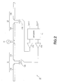
- the tunable antenna 1 As the fundamental configuration thereof is shown in FIG. 2, two antenna elements 11, 12 constituting ⁇ /2 dipole antenna are respectively bisected, and a switch 13A for connecting the bisected antenna elements 11A, 11B therebetween and a switch 13B for connecting the bisected antenna elements 12A, 12B therebetween are provided at the bisected (divisional) positions so that structure resonating at two kinds of frequency bands is provided.
- the switches 13A, 13B are opened, the tunable antenna 1 functions as ⁇ a/2 dipole antenna resonating at the frequency band of the high frequency band side only by two antenna elements 11A, 12A of feed-point side connected to a RF power feed terminal 16.
- the switches 13A, 13B are closed, the tunable antenna 1 functions as ⁇ b/2 dipole antenna by the entirety of the antenna elements 11A, 11B, 12A, 12B which have been bisected.
- the tunable antenna 1 is caused to be of the structure in which wavelength where resonating operation takes place at 5.2 GHz band is caused to be ⁇ a, wavelength where resonating operation is performed at 2.4 GHz band is caused to be ⁇ b, lengths of respective antenna elements 11A, 12A of the feed-point side are caused to be ⁇ a/4, and antenna elements 11B, 12B having length of ( ⁇ b - Xa)/4 are connected to respective antenna elements 11A, 12A of the feed-point side through the switch 13B, whereby in the state where the switches 13A, 13B are opened, the tunable antenna 1 functions as ⁇ a/2 dipole antenna resonating at 5.2 GHz band used for data communication in conformity with the IEEE802.
- the tunable antenna 1 functions as ⁇ b/2 dipole antenna resonating at 2.4 GHz band used for data communication in conformity with the IEEE802.
- 11b by the entirety of the antenna elements 11A, 11B, 12A, 12B which have been bisected.
- switches 13A, 13B there are respectively used MEMS (Micro-Electro-Mechanical-System) switches.
- Control signals (cont1, cont2) are delivered from the system control unit 6 to drivers 14A, 14B for driving the respective switches 13A, 13B through a decoder 15.
- the operation mode is communication mode in conformity with the IEEE802. 11a
- the respective switches 13A, 13B are placed in opened state.
- the operation mode is communication mode inconformity with the IEEE802. 11b
- these switches are placed in closed state.
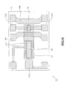
- FIG. 3 shows the configuration example of the tunable antenna 1 in which symmetry-type dipole antenna excited (driven) from feed-point is formed on printed wiring board.
- a power feed terminal section 110 bisected folded pattern-shaped respective antenna element patterns 111A, 111B, 112A, 112B, and MEMS switch elements 113A, 113B located at the bisected positions.
- the length of one side dipole element is approximately 1/4 ⁇ (substantially Rout( ⁇ ) in material having dielectric constant ⁇ ). Switching of a desired length is performed by MEMS switch elements 113A, 113B, thereby making it possible to change resonance frequency as shown in FIG. 4.
- FIG. 4 shows the state of band tuning of the tunable antenna 1 in which there is formed ⁇ /2 dipole antenna capable of switching resonance band into two kinds of frequency bands of 5.2GHz band and 2.4 GHz band by the MEMS switch elements (SW1, 2) 113A, 113B.
- the abscissa indicates frequency (GHz), and the ordinate indicates insertion loss (dB).
- the tunable antenna 1 functions as a dual band antenna in which in the state where MEMS switch elements 113A, 113B are opened, the tunable antenna 1 resonates at 5.2GHz band, and in the state where the MEMS switch elements 113A, 113B are closed, the tunable antenna 1 resonates at 2.4GHz band.
- MEMS switch elements 113A, 113B used as respective switches 13A, 13B of the tunable antenna 1 have similar structure, only the structure of the MEMS switch element 113 will be explained.
- the MEMS switch element 113 is composed of a silicon substrate 130 where first and second control electrode patterns 131A, 131B, first and second ground patterns 132A, 132B, and first and second fixed contact electrode patterns 133A, 133B are formed in the state where they are insulated from each other, and a cantilever 134 comprised of thin plate shaped insulating material having elasticity, which is supported in the cantilever state as the result of the fact that one end thereof is fixed at the position of the first control electrode pattern 131A on the silicon substrate 130.
- an opposite electrode pattern 135 electrically connected to the first control electrode pattern 131A and extended up to the position opposite to the second control electrode pattern 131B.
- a movable contact piece 136 at the free end side thereof, in a manner opposite to both the first and second fixed contact electrode patterns 133A, 133B.
- the MEMS switch element 113 of such a structure when drive signals are delivered from the drivers 14A, 14B to the first and second control electrode patterns 131A, 131B, electrostatic attractive force is produced by drive voltage applied to the opposite portion of the first and second control electrode patterns 131A, 131B.
- the cantilever 134 of the cantilever support structure is bent.
- the cantilever 134 when drive signals for applying drive voltage of reverse bias are delivered from drivers 14A, 14B to the first and second control electrode patterns 131A, 131B in the closed state, the cantilever 134 returns to the initial state so that the movable contact piece 136 is away from the first and second fixed contact electrode patterns 133A, 133B, the MEMS switch element 113 is placed in closed state.
- the MEMS switch element 113 is mounted by the processing as described below. Namely, the MEMS switch element 113 is mounted after undergone positioning on an organic base substrate 100A where wiring patterns 120 are formed as shown in FIG. 7A in the state where the silicon substrate 130 is caused to be located at the upper side as shown in FIG. 7B to hold opposite spacing by metallic ball bumps 121. Further, ultrasonic wave is applied while pressurizing the metallic ball bumps 121 on the order of several ten grams in the state where, e.g., the organic base substrate 100A is heated so that its temperature is 80°C to 120°C to thereby mount the MEMS switch element 113 on the organic base substrate 100A.
- the method of mounting MEMS switch element 113 is not limited to such ultrasonic flip-chip mounting method, but suitable bare chip mounting method may be employed.
- a cap substrate 100B where shield pattern 122 is formed is further mounted and bonded on the organic base substrate 100A on which MEMS switch element 113 is mounted in this way.
- a recessed portion 123 having dimensions sufficient to cover the MEMS switch element 113 is formed at the bonding surface to the organic base substrate 100A.
- the shield pattern 122 is formed as film at the recessed portion 123 by the MID (Molded Interconnect Device) method or deposition method, etc. for three-dimensionally forming electric circuit patterns with respect to, e.g., resin molded material.
- the cap substrate 100B is bonded onto the organic base substrate 100A in a manner as described below.
- the organic base substrate 100A and the cap substrate 100B are integrated by, e.g., ultrasonic wave welding method in the state where the cap substrate 100B is overlaid with respect to the organic base substrate 100A after undergone positioning.
- the organic base substrate 100A and the cap substrate 100B are adapted to accommodate MEMS switch 113 in the state where nitrogen is sealed within a MEMS switch accommodating space section 124 constituted by the recessed portion 123 under bonded condition. Accordingly, since the MEMS switch element 113 is mounted into the MEMS switch accommodating space portion 124 in the state where moisture resistance characteristic and oxidation resistance characteristic are maintained, oxidation of respective components and/or sticking of the movable contact piece 136, etc. are prevented. Thus, improvement in durability and operating stability can be realized. As a result, it is possible to prevent high frequency loss and to form the entirety of the antenna by the compact structure.
- the MEMS switch element 113 of the antenna board 100 where the organic base substrate 100A and the cap substrate 100B are bonded in this way is buried, and antenna element patterns 125A, 125B connected, through vias 126A, 126B, to the wiring patterns 120 formed on the organic base substrate 100A are formed as film on the cap substrate 100B.
- the first transmitting/receiving circuit 4 and the second transmitting/receiving circuit 5 are connected to the tunable antenna 1 through the duplexer 2 and the first and second transmit/receive changeover switches 3A, 3B.
- the operations of the first and second transmit/receive changeover switches 3A, 3B are controlled by the system control unit 6 in a manner as described later.
- the first trtansmitting/receiving circuit 4 is composed of a digital control unit 40 and a RF front end unit 140 which employs Orthogonal Frequency Division Multiplexing (OFDM) system as modulation system for transmit data to perform data communication A in conformity with the IEEE802. 11a at carrier of 5.2 GHz band.
- OFDM Orthogonal Frequency Division Multiplexing
- the digital control unit 40 is composed of a CPU41, a flash memory 42, a digital physical layer 43, and a MAC (Media Access Control) 44, etc., and serves to generate transmit data to send the transmit data thus generated to the RF front end unit 140, and to receive demodulated receive data from the RF front end unit 140.
- the RF front end unit 140 is composed of a transmitting block 240, a receiving block 340 and a local oscillation block 440.
- the transmitting block 240 is composed of a data conversion unit 242 supplied with transmit data from the digital control unit 40 through a demultiplexer (DEMUX) 241, a D/A converting unit 243 connected to the data converting unit 242, a modulation unit 244 connected to the D/A converting unit 243, a power amplifier unit 245 supplied with modulated output of the modulation processing unit 244, and a distortion compensation processing unit (digital predistortion) 246 for compensating signal distortion taking place at the power amplifier unit 245, etc.
- DEMUX demultiplexer
- D/A converting unit 243 connected to the data converting unit 242
- modulation unit 244 connected to the D/A converting unit 243
- a power amplifier unit 245 supplied with modulated output of the modulation processing unit 244
- a distortion compensation processing unit (digital predistortion) 246 for compensating signal distortion taking place at the power amplifier unit 245, etc.
- the data converting unit 242 serves to convert transmit data (time series data) delivered through the demultiplexer (DEMUX) 241 from serial data to parallel data to thereby allocate bits of the transmit data to respective carriers to be transmitted to perform Inverse- Fast Fourier Transform (1-FFT) to thereby transform the data thus obtained into data of time region.
- DEMUX demultiplexer
- 1-FFT Inverse- Fast Fourier Transform
- the D/A converting unit 243 serves to convert transmit data of the time region allocated to respective carriers into analog signal by the data converting unit 242 to deliver the analog signal thus obtained to the modulation unit 244.
- the modulation unit 244 modulates orthogonal carriers by the transmit data of the time region which has been converted into the analog signal by the D/A converting unit 243.
- the power amplifier unit 245 serves to amplify orthogonally modulated signal obtained by the modulation unit 244.
- the orthogonally modulated signal which has been amplified by the power amplifier unit 245 is delivered to the tunable antenna 1 through the first transmit/receive changeover switch 3A and the duplexer 2.
- the distortion compensation processing unit 246 performs, in advance, distortion compensation processing for compensating signal distortion taking place in orthogonally modulated signal outputted from the power amplifier unit 245 with respect to transmit data of the time region which has been allocated to respective carriers.
- the receiving block 340 serves to perform processing opposite to that of the transmitting block 240, and is composed of a RF amplifier unit 341, a demodulation unit 342, an A/D converting unit 343, a data inverting unit 344, and a multiplexer (MUX) 345.
- a RF amplifier unit 341 a demodulation unit 342, an A/D converting unit 343, a data inverting unit 344, and a multiplexer (MUX) 345.
- MUX multiplexer
- the RF amplifier unit 341 serves to amplify receive signal delivered, through the duplexer 2 and the first transmit/receive changeover switch 3A, from the tunable antenna 1 to deliver the signal thus obtained to the demodulation unit 342.
- the demodulation unit 342 serves to multiply receive signal (orthogonally modulated signal) delivered from the RF amplifier unit 341 by orthogonal carriers to thereby modulate an analog signal of receive data of the time region in which bits are allocated to respective carriers.
- the A/D converting unit 343 digitizes the analog signal of the receive data of the time region to thereby convert is into receive data of the time region to deliver the receive data thus obtained to the data inverting unit 344, and to deliver reception intensity signal (RSSI_A) indicated by amplitude value of analog signal of receive data of the time region to the system control unit 6.
- RSSI_A reception intensity signal
- the data inverting unit 344 converts receive data of the frequency region obtained by performing Inverse-Fast Fourier Transform (I-FFT) of receive data of the time region delivered from the A/D converting unit 343 from serial data to parallel data to deliver the parallel data thus obtained to the digital control unit 40 through multiplexer (DEMUX).
- I-FFT Inverse-Fast Fourier Transform
- the local oscillation block 440 is composed of a voltage controlled oscillator (VCO) 441 for generating orthogonal two-phase signal of 5.2 GHz band, and a PLL circuit for performing PLL control of the VCO 441, and serves to deliver the orthogonal two-phase signal obtained by the VCO 441 to the modulation unit 244 of the transmitting block 240 as orthogonal carrier for transmission, and to deliver the orthogonal two-phase signal to the demodulation unit 342 of the receiving block 340 as orthogonal carrier for orthogonal modulation.
- VCO voltage controlled oscillator
- the second transmitting/receiving circuit 5 is composed of a digital control unit 50 and a RF front end unit 150 which employ Orthogonal Frequency Division Multiplexing (OFDM) system as modulation system for transmit data to perform data communication B in conformity with the IEEE802. 11b at carrier of 2.4 GHz band.
- OFDM Orthogonal Frequency Division Multiplexing
- the digital control unit 50 is composed of a CPU51, a flash memory 52, a digital physical layer 53, and a MAC (Media Access Control) 54, etc., and serves to generate transmit data to send the transmit data thus generated to the RF front end unit 150 to receive demodulated receive data from the RF front end unit 150.
- the RF front end unit 150 is composed of a transmitting block 250, a receiving block 350, and a local oscillation block 450.
- the transmitting block 250 is composed of a data converting unit 252 supplied with transmit data from the digital control unit 50 through a demultiplexer (DEMUX) 251, a D/A converting unit 253 connected to the data converting unit 252, a modulation unit 254 connected to the D/A converting unit 253, etc, a power amplifier unit 255 supplied with modulated output of the modulation processing unit 254, and a distortion compensation processing unit (digital predistortion) 256 for compensating signal distortion taking place at the power amplifier unit 255, etc.
- DEMUX demultiplexer
- D/A converting unit 253 connected to the data converting unit 252
- modulation unit 254 connected to the D/A converting unit 253, etc
- a power amplifier unit 255 supplied with modulated output of the modulation processing unit 254
- a distortion compensation processing unit digital predistortion
- the data converting unit 252 serves to convert transmit data (time series data) delivered through the demoultiplexer (DEMUX) 251 from serial data to parallel data to thereby allocate bits of transmit data to respective carriers to be transmitted to perform Inverse-Fast Fourier Transform (I-FFT) to transform it into data of the time region.
- transmit data time series data
- DEMUX demoultiplexer
- I-FFT Inverse-Fast Fourier Transform
- the D/A converting unit 253 serves to convert transmit data of the time region which has been allocated to respective carriers into an analog signal by the data converting unit 252 to deliver the analog signal thus obtained to the modulation unit 254.
- the modulation unit 254 modulates orthogonal carrier by transmit data of the time region which has been converted into analog signal by the D/A converting unit 253.
- the power amplifier unit 255 amplifies orthogonally modulated signal obtained by the modulation unit 254.
- the orthogonally modulated signal which has been amplified by the power amplifier unit 255 is delivered to the tunable antenna 1 through the first transmit/receive changeover switch 3B and the duplexer 2.
- the distortion compensation processing unit 256 performs, in advance, distortion compensation processing for compensating signal distortion taking place in orthogonally modulated signal outputted from the power amplifier unit 255 with respect to transmit data of the time region which has been allocated to respective carriers.
- the receiving block 350 serves to perform processing opposite to that of the transmitting block 250, and is composed of a RF amplifier unit 351, a demodulation unit 352, an A/D converting unit 353, a data inverting unit 354, and a multiplexer (MUX) 355.
- a RF amplifier unit 351 a demodulation unit 352, an A/D converting unit 353, a data inverting unit 354, and a multiplexer (MUX) 355.
- MUX multiplexer
- the RF amplifier unit 351 amplifiers receive signal delivered, through the duplexer 2 and the second transmit/receive changeover switch 3B, from the tunable antenna 1 to deliver the signal thus obtained to the demodulation unit 352.
- the demodulation unit 352 serves to multiply receive signal (orthogonally modulated signal) delivered from the RF amplifier unit 351 by orthogonal carriers to thereby demodulate an analog signal of receive data of the time region where bits are allocated to respective carriers.
- the A/D converting unit 353 digitizes the analog signal of the receive data of the time region to thereby convert it into receive data of the time region to deliver the receive data of the time region to the data inverting unit 354, and to deliver reception intensity signal (RSSI_B) indicated by amplitude value of the analog signal of the receive data of the time region to the system control unit 6.
- RSSI_B reception intensity signal
- the data inverting unit 354 converts receive data of the frequency region obtained by performing Inverse-Fast Fourier Transform (I-FFT) of the receive data of the time region delivered from the A/D converting unit 353 from serial data to parallel data to deliver the receive data thus obtained to the digital control unit 50 through the multiplexer (MUX) 355.
- I-FFT Inverse-Fast Fourier Transform
- the local oscillation block 450 is composed of a voltage controlled oscillator (VCO) 451 for generating orthogonal two-phase signal of 2.4 GHz band, and a PLL circuit 452 for performing PLL control of the VCO 451, and serves to deliver orthogonal two-phase signal obtained by the VCO 451 to the modulation unit 254 of the transmitting block 250 as orthogonal carrier for transmission, and to deliver the orthogonal two-phase signal to the demodulation unit 352 of the receiving block 350 as orthogonal carrier for orthogonal modulation.
- VCO voltage controlled oscillator
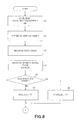
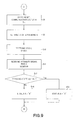
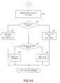
- system control unit 6 controls the wireless communication system 10 in accordance with the procedure shown in the flowcharts of FIGS. 8 to 10.
- the system control unit 6 allows the entirety of the wireless communication system 10 to be in reset state thereafter to allow the operation mode to be communication mode in conformity with the IEEE802.
- 11b where data communication B is performed by the second transmitting/receiving circuit 5 (step S1) to allow control signals (cont1, cont2) to be turned ON to allow respective switches 13A, 13B of the tunable antenna 1 to be placed in closed state to thereby make a setting such that the tunable antenna 1 functions as ⁇ b/2 dipole antenna resonating at 2.4GHz band used in data communication B in conformity with the IEEE802. 11b (step S2).
- the local oscillation block 440 of the second transmitting/receiving circuit 5 is controlled to perform frequency scan (step S3) to judge, while monitoring reception intensity signal (RSSI_B) of the second transmitting/receiving circuit 5 (step S4), whether or not data communication B in conformity with the IEEE802. 11b can be made (step S5).
- step S5 i.e., data communication B in conformity with the IEEE802. 11b can be made, status B indicating available/non-available (usable/unusable) state of the data communication B in conformity with the IEEE802. 11b is caused to be "0" to store that status B into memory (step S6).
- step S7 in the case where judgment result at the step S5 is NO, i.e., data communication B in conformity with the IEEE802. 11b cannot be made, status B indicating available/non-available state of data communication B in conformity with the IEEE802. 11b is caused to be "0" to store that status B into memory (step S7).
- the system control unit 6 allows the entirety of the wireless communication system 10 to be in reset state to allow the operation mode to be communication mode in conformity with the IEEE802.
- 11a where data communication A is performed by the first transmitting/receiving circuit 4 (step S8) to allow control signals (cont1, cont2) to be turned OFF to allow respective switches 13A, 13B of the tunable antenna 1 to be placed in opened state to thereby make a setting such that the tunable antenna 1 functions as ⁇ a/2 dipole antenna resonating at 5.2 GHz band used for data communication A in conformity with the IEEE802. 11a (step S9).
- the local oscillation block 440 of the first transmitting/receiving circuit 4 is controlled to perform frequency Scan (step S10) to judge, while monitoring reception intensity signal (RSSI_A) of the first transmitting/receiving circuit 4 (step S11), whether or not data communication A in conformity with the IEEE802. 11a can be made (step S12).
- RSSI_A reception intensity signal
- step S12 i.e., data communication A in conformity with the IEEE802. 11a can be made, status A indicating available/non-available state of the data communication A in conformity with the IEEE802. 11a is caused to be "0" to store that status A into memory (step S13).
- step S12 i.e., data communication A in conformity with the IEEE802. 11a cannot be made
- status A indicating available/non-available state of the data communication A in conformity with the IEEE802. 11a is caused to be "0" to store that status A into memory (step S14).
- the system control unit 6 judges, in this way, available/non-available state of data communication A in conformity with the IEEE802. 11a and data communication B in conformity with the IEEE802. 11b to store, into memory, the status A and the status B which indicate the available/non-available state of data communication A and data communication B (step S 15).
- the system control unit 6 checks the status A and the status B which have been stored in the memory (step S16). When both the data communication A and the data communication B can be used, the system control unit 6 checks whether or not current state of the slave device is desired communication mode (power saving mode or high communication Rate mode) (step S17).
- control signals (cont1, cont2) are caused to be turned ON to fix the communication mode to the receiving mode at the data communication B in conformity with the IEEE802. 11b (step S 18).
- control signals (cont1, cont2) are caused to be turned OFF to perform tuning so that receiving sensitivity of the tunable antenna 1 is set to 5.2 GHz band thereafter to set the communication mode to the receiving mode at the data communication A in conformity with the IEEE802. 11a (step S19).
- the system control unit 6 serves to compulsorily fix the communication mode to usable communication system to display a notification that current communication mode is compulsory mode (step S20).
- the system control unit 6 displays that data communication cannot be used to allow the communication to be turned “OFF” (step S21).
- control signals (cont1, cont2) are generated at the system control unit 6 on the basis of reception intensity signals (RSSI signals) obtained by respective transmitting/receiving circuits 4, 5 to switch the operation mode, thereby making it possible to automatically select reasonable communication mode to perform data communication.
- RSSI signals reception intensity signals
- the previously described available/non-available state of two data communication systems may be monitored, e.g., at specific time interval, whereby when either one communication system is placed in unusable state for any cause, e.g., when waking is made from the sleep mode and/or the state is reset, etc., switching into either one usable system can be also automatically performed.
- ⁇ /2 dipole antenna including folded pattern-shaped antenna element patterns 111A, 111B, 112A, 112A, 112B is used as the tunable antenna 1 in the above-described example
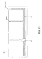
- the length of antenna element pattern 211 may be switched by MEMS switch element 213 at inverted F-type mono-pole antenna 210 as shown in FIG. 11 to change resonance frequency
- antenna element patterns 311 may be switched by MEMS switch element 313 at micro-strip fed slot type antenna 310 as shown in FIG. 12 to change resonance frequency.
- the multi-layer structure of multi-layer printed wiring board may be utilized to constitute antenna of three-dimensional structure to perform switching by MEMS switch elements.
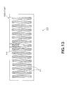
- resonance frequency may be switched by MEMS switch element 413 at mono-pole antenna 410 having antenna patterns 411 of spiral shape formed by making use of multi-layer structure of the multi-layer printed wiring board.
- troublesomeness in which plural communication systems are used while performing selective switching thereof can be eliminated.
- user can select and use communication system corresponding to the environment and/or use state at that place without becoming conscious that any communication is used.
- MEMS switch elements are included within the printed wiring board, thereby making it possible to provide compact configuration with low power consumption.
Landscapes
- Transceivers (AREA)
- Variable-Direction Aerials And Aerial Arrays (AREA)
- Details Of Aerials (AREA)
Applications Claiming Priority (3)
| Application Number | Priority Date | Filing Date | Title |
|---|---|---|---|
| JP2002378431 | 2002-12-26 | ||
| JP2002378431A JP2004214726A (ja) | 2002-12-26 | 2002-12-26 | 無線通信アンテナ及び無線通信装置 |
| PCT/JP2003/015884 WO2004059791A1 (ja) | 2002-12-26 | 2003-12-11 | 無線通信アンテナ及び無線通信装置 |
Publications (2)
| Publication Number | Publication Date |
|---|---|
| EP1580841A1 true EP1580841A1 (de) | 2005-09-28 |
| EP1580841A4 EP1580841A4 (de) | 2006-01-18 |
Family
ID=32677430
Family Applications (1)
| Application Number | Title | Priority Date | Filing Date |
|---|---|---|---|
| EP03778825A Withdrawn EP1580841A4 (de) | 2002-12-26 | 2003-12-11 | Antenne zur drahtlosen kommunikation und vorrichtung zur drahtlosen kommunikation |
Country Status (5)
| Country | Link |
|---|---|
| US (1) | US20060079177A1 (de) |
| EP (1) | EP1580841A4 (de) |
| JP (1) | JP2004214726A (de) |
| KR (1) | KR20050088330A (de) |
| WO (1) | WO2004059791A1 (de) |
Cited By (6)
| Publication number | Priority date | Publication date | Assignee | Title |
|---|---|---|---|---|
| EP1826873A1 (de) | 2006-02-27 | 2007-08-29 | Alps Electric Co., Ltd. | Antenne mit verbesserter Empfangsempfindlichkeit im Breitband |
| US7315287B2 (en) | 2004-11-09 | 2008-01-01 | Alps Electric Co., Ltd. | Antenna device having enhanced reception sensitivity in wide bands |
| WO2009130369A1 (en) * | 2008-04-25 | 2009-10-29 | Nokia Corporation | Method for enhancing an antenna performance, antenna, and apparatus |
| CN101098040B (zh) * | 2007-05-29 | 2011-07-06 | 东南大学 | 平面转折射频袖珍隐形天线 |
| EP2071733A3 (de) * | 2007-12-13 | 2012-07-25 | Broadcom Corporation | Verfahren und System für in einem integrierten Schaltungspaket hergestellte MEMS-Schalter |
| GB2522941A (en) * | 2013-12-19 | 2015-08-12 | Cambridge Silicon Radio Ltd | Apparatus for wirelessly charging a rechargeable battery |
Families Citing this family (27)
| Publication number | Priority date | Publication date | Assignee | Title |
|---|---|---|---|---|
| US8743837B2 (en) | 2003-04-10 | 2014-06-03 | Qualcomm Incorporated | Modified preamble structure for IEEE 802.11A extensions to allow for coexistence and interoperability between 802.11A devices and higher data rate, MIMO or otherwise extended devices |
| US7916803B2 (en) | 2003-04-10 | 2011-03-29 | Qualcomm Incorporated | Modified preamble structure for IEEE 802.11a extensions to allow for coexistence and interoperability between 802.11a devices and higher data rate, MIMO or otherwise extended devices |
| US7586884B2 (en) | 2003-08-15 | 2009-09-08 | Qualcomm Incorporated | Joint packet detection in wireless communication system with one or more receiver |
| US7539260B2 (en) | 2004-05-27 | 2009-05-26 | Qualcomm Incorporated | Detecting the number of transmit antennas in wireless communication systems |
| US7239290B2 (en) * | 2004-09-14 | 2007-07-03 | Kyocera Wireless Corp. | Systems and methods for a capacitively-loaded loop antenna |
| US7408517B1 (en) * | 2004-09-14 | 2008-08-05 | Kyocera Wireless Corp. | Tunable capacitively-loaded magnetic dipole antenna |
| US7348928B2 (en) * | 2004-12-14 | 2008-03-25 | Intel Corporation | Slot antenna having a MEMS varactor for resonance frequency tuning |
| JP4834077B2 (ja) * | 2005-03-21 | 2011-12-07 | クゥアルコム・インコーポレイテッド | 1またはそれ以上の受信器を備えた無線通信システムにおける統合パケット検出 |
| JP2007021713A (ja) * | 2005-06-17 | 2007-02-01 | Semiconductor Energy Lab Co Ltd | 半導体装置、およびその作製方法 |
| JP4704287B2 (ja) * | 2005-08-02 | 2011-06-15 | パナソニック株式会社 | アンテナ装置および携帯無線機 |
| KR100878750B1 (ko) * | 2005-09-23 | 2009-01-14 | 삼성전자주식회사 | 직교주파수 다중분할방식 네트워크에서 협력적중계를 위한혼종 포워딩 장치 및 방법 |
| US7746815B2 (en) | 2005-09-23 | 2010-06-29 | Samsung Electronics Co., Ltd | Hybrid forwarding apparatus and method for cooperative relaying in an OFDM network |
| CN1983714A (zh) * | 2005-12-14 | 2007-06-20 | 三洋电机株式会社 | 多频段终端天线及使用其的天线系统 |
| KR100922001B1 (ko) * | 2007-09-10 | 2009-10-14 | 한국전자통신연구원 | 교차 다이폴, 교차 다이폴 모듈, 배열 안테나 및 다중 입력다중 출력 안테나 |
| JP4603617B2 (ja) * | 2008-11-27 | 2010-12-22 | 京セラ株式会社 | 通信機器 |
| JP5321290B2 (ja) * | 2009-06-30 | 2013-10-23 | 株式会社村田製作所 | アンテナ構造 |
| EP2478471A1 (de) * | 2009-09-14 | 2012-07-25 | Ingecom Sàrl | Identifikationsmodul mit aktiver kennzeichnung |
| JP4738526B2 (ja) * | 2009-11-26 | 2011-08-03 | 株式会社東芝 | 電子機器 |
| JP5092035B2 (ja) * | 2011-04-25 | 2012-12-05 | 株式会社東芝 | 電子機器 |
| JP5742491B2 (ja) | 2011-06-09 | 2015-07-01 | ソニー株式会社 | 通信制御装置、無線通信端末、処理実行装置、通信システムおよび通信制御方法 |
| KR102062212B1 (ko) * | 2013-10-04 | 2020-01-03 | 삼성전자주식회사 | 전자 기기의 안테나 장치 |
| US9791470B2 (en) * | 2013-12-27 | 2017-10-17 | Intel Corporation | Magnet placement for integrated sensor packages |
| US9502775B1 (en) * | 2014-04-16 | 2016-11-22 | Google Inc. | Switching a slot antenna |
| US10347967B2 (en) * | 2016-01-26 | 2019-07-09 | Qualcomm Incorporated | Signal delivery and antenna layout using flexible printed circuit board (PCB) |
| JP2019101735A (ja) * | 2017-12-01 | 2019-06-24 | 東芝テック株式会社 | Rfidタグ |
| US12362481B2 (en) * | 2022-06-29 | 2025-07-15 | Beijing Boe Technology Development Co., Ltd. | Tunable antenna, method for preparing the same, and electronic device using the same |
| CN117458151A (zh) * | 2023-11-27 | 2024-01-26 | 维沃移动通信有限公司 | 天线装置和电子设备 |
Family Cites Families (11)
| Publication number | Priority date | Publication date | Assignee | Title |
|---|---|---|---|---|
| US6061025A (en) * | 1995-12-07 | 2000-05-09 | Atlantic Aerospace Electronics Corporation | Tunable microstrip patch antenna and control system therefor |
| US6069587A (en) * | 1998-05-15 | 2000-05-30 | Hughes Electronics Corporation | Multiband millimeterwave reconfigurable antenna using RF mem switches |
| GB2354115A (en) * | 1999-09-09 | 2001-03-14 | Univ Surrey | Adaptive multifilar antenna |
| US6853067B1 (en) * | 1999-10-12 | 2005-02-08 | Microassembly Technologies, Inc. | Microelectromechanical systems using thermocompression bonding |
| US6417807B1 (en) * | 2001-04-27 | 2002-07-09 | Hrl Laboratories, Llc | Optically controlled RF MEMS switch array for reconfigurable broadband reflective antennas |
| JP2001148609A (ja) * | 1999-11-19 | 2001-05-29 | Kojima Press Co Ltd | アンテナ、平衡不平衡変換器および受信機 |
| JP4348498B2 (ja) * | 2000-07-17 | 2009-10-21 | ソニー株式会社 | 無線通信機器 |
| GB0030741D0 (en) * | 2000-12-16 | 2001-01-31 | Koninkl Philips Electronics Nv | Antenna arrangement |
| JP2002232319A (ja) * | 2001-02-01 | 2002-08-16 | Fujitsu Ltd | 情報処理装置および通信監視制御プログラム |
| JP3469880B2 (ja) * | 2001-03-05 | 2003-11-25 | ソニー株式会社 | アンテナ装置 |
| WO2002096166A1 (en) * | 2001-05-18 | 2002-11-28 | Corporation For National Research Initiatives | Radio frequency microelectromechanical systems (mems) devices on low-temperature co-fired ceramic (ltcc) substrates |
-
2002
- 2002-12-26 JP JP2002378431A patent/JP2004214726A/ja not_active Abandoned
-
2003
- 2003-12-11 US US10/540,647 patent/US20060079177A1/en not_active Abandoned
- 2003-12-11 KR KR1020057011958A patent/KR20050088330A/ko not_active Withdrawn
- 2003-12-11 WO PCT/JP2003/015884 patent/WO2004059791A1/ja not_active Ceased
- 2003-12-11 EP EP03778825A patent/EP1580841A4/de not_active Withdrawn
Cited By (10)
| Publication number | Priority date | Publication date | Assignee | Title |
|---|---|---|---|---|
| US7315287B2 (en) | 2004-11-09 | 2008-01-01 | Alps Electric Co., Ltd. | Antenna device having enhanced reception sensitivity in wide bands |
| EP1826873A1 (de) | 2006-02-27 | 2007-08-29 | Alps Electric Co., Ltd. | Antenne mit verbesserter Empfangsempfindlichkeit im Breitband |
| CN101098040B (zh) * | 2007-05-29 | 2011-07-06 | 东南大学 | 平面转折射频袖珍隐形天线 |
| EP2071733A3 (de) * | 2007-12-13 | 2012-07-25 | Broadcom Corporation | Verfahren und System für in einem integrierten Schaltungspaket hergestellte MEMS-Schalter |
| US8384500B2 (en) | 2007-12-13 | 2013-02-26 | Broadcom Corporation | Method and system for MEMS switches fabricated in an integrated circuit package |
| WO2009130369A1 (en) * | 2008-04-25 | 2009-10-29 | Nokia Corporation | Method for enhancing an antenna performance, antenna, and apparatus |
| US7773044B2 (en) | 2008-04-25 | 2010-08-10 | Nokia Corporation | Method for enhancing an antenna performance, antenna, and apparatus |
| GB2522941A (en) * | 2013-12-19 | 2015-08-12 | Cambridge Silicon Radio Ltd | Apparatus for wirelessly charging a rechargeable battery |
| US9325184B2 (en) | 2013-12-19 | 2016-04-26 | Qualcomm Technologies International, Ltd. | Apparatus for wirelessly charging a rechargeable battery |
| GB2522941B (en) * | 2013-12-19 | 2020-08-05 | Qualcomm Technologies Int Ltd | Apparatus for wirelessly charging a rechargeable battery |
Also Published As
| Publication number | Publication date |
|---|---|
| US20060079177A1 (en) | 2006-04-13 |
| EP1580841A4 (de) | 2006-01-18 |
| KR20050088330A (ko) | 2005-09-05 |
| JP2004214726A (ja) | 2004-07-29 |
| WO2004059791A1 (ja) | 2004-07-15 |
Similar Documents
| Publication | Publication Date | Title |
|---|---|---|
| US20060079177A1 (en) | Wireless communicatin antenna and wireless communication device | |
| US6124831A (en) | Folded dual frequency band antennas for wireless communicators | |
| CN102394372B (zh) | 电子设备和可调谐天线系统 | |
| US6480155B1 (en) | Antenna assembly, and associated method, having an active antenna element and counter antenna element | |
| CN103296384B (zh) | 用于手持式设备的可调谐天线 | |
| CN203071220U (zh) | 电子装置和天线 | |
| US7358902B2 (en) | Dual-band antenna for a wireless local area network device | |
| US7831230B2 (en) | Terminal and associated transducer assembly and method for selectively transducing in at least two frequency bands | |
| US20010050643A1 (en) | Small-size broad-band printed antenna with parasitic element | |
| CN100530987C (zh) | 天线装置及使用该天线装置的无线电通信设备 | |
| JP2004519916A (ja) | モジュール及び電子デバイス | |
| CN103337702A (zh) | 带有滤波器和调谐电路的电子设备天线 | |
| EP1387435A1 (de) | Antenneneinrichtung | |
| US20040160368A1 (en) | Dual-band antenna | |
| US8155607B2 (en) | Antenna apparatus of portable terminal | |
| JP2005535239A (ja) | デュアルバンドアンテナシステム | |
| KR100640365B1 (ko) | 휴대용 단말기의 안테나 장치 | |
| JP4112178B2 (ja) | アンテナ装置及び無線機 | |
| US20020075185A1 (en) | Concealed antenna for mobile communication device | |
| JPH11251981A (ja) | 移動通信機 | |
| JPH08307303A (ja) | 携帯無線機 | |
| US6414640B1 (en) | Antenna assembly, and associated method, which exhibits circular polarization | |
| US20010045909A1 (en) | Electronic device having a compact antenna assembly which exhibits circular polarization | |
| US20050128157A1 (en) | Multi-band cable antenna | |
| JPH1032426A (ja) | アンテナ装置 |
Legal Events
| Date | Code | Title | Description |
|---|---|---|---|
| PUAI | Public reference made under article 153(3) epc to a published international application that has entered the european phase |
Free format text: ORIGINAL CODE: 0009012 |
|
| 17P | Request for examination filed |
Effective date: 20050624 |
|
| AK | Designated contracting states |
Kind code of ref document: A1 Designated state(s): AT BE BG CH CY CZ DE DK EE ES FI FR GB GR HU IE IT LI LU MC NL PT RO SE SI SK TR |
|
| A4 | Supplementary search report drawn up and despatched |
Effective date: 20051206 |
|
| RBV | Designated contracting states (corrected) |
Designated state(s): DE FR GB |
|
| 17Q | First examination report despatched |
Effective date: 20060705 |
|
| 17Q | First examination report despatched |
Effective date: 20060705 |
|
| STAA | Information on the status of an ep patent application or granted ep patent |
Free format text: STATUS: THE APPLICATION HAS BEEN WITHDRAWN |
|
| 18W | Application withdrawn |
Effective date: 20080515 |