EP1580604A2 - Stage device and exposure apparatus - Google Patents
Stage device and exposure apparatus Download PDFInfo
- Publication number
- EP1580604A2 EP1580604A2 EP05251631A EP05251631A EP1580604A2 EP 1580604 A2 EP1580604 A2 EP 1580604A2 EP 05251631 A EP05251631 A EP 05251631A EP 05251631 A EP05251631 A EP 05251631A EP 1580604 A2 EP1580604 A2 EP 1580604A2
- Authority
- EP
- European Patent Office
- Prior art keywords
- substrate
- region
- stator unit
- exposure
- coil group
- Prior art date
- Legal status (The legal status is an assumption and is not a legal conclusion. Google has not performed a legal analysis and makes no representation as to the accuracy of the status listed.)
- Withdrawn
Links
Images


Classifications
-
- F—MECHANICAL ENGINEERING; LIGHTING; HEATING; WEAPONS; BLASTING
- F16—ENGINEERING ELEMENTS AND UNITS; GENERAL MEASURES FOR PRODUCING AND MAINTAINING EFFECTIVE FUNCTIONING OF MACHINES OR INSTALLATIONS; THERMAL INSULATION IN GENERAL
- F16B—DEVICES FOR FASTENING OR SECURING CONSTRUCTIONAL ELEMENTS OR MACHINE PARTS TOGETHER, e.g. NAILS, BOLTS, CIRCLIPS, CLAMPS, CLIPS OR WEDGES; JOINTS OR JOINTING
- F16B7/00—Connections of rods or tubes, e.g. of non-circular section, mutually, including resilient connections
- F16B7/18—Connections of rods or tubes, e.g. of non-circular section, mutually, including resilient connections using screw-thread elements
- F16B7/187—Connections of rods or tubes, e.g. of non-circular section, mutually, including resilient connections using screw-thread elements with sliding nuts or other additional connecting members for joining profiles provided with grooves or channels
-
- G—PHYSICS
- G03—PHOTOGRAPHY; CINEMATOGRAPHY; ANALOGOUS TECHNIQUES USING WAVES OTHER THAN OPTICAL WAVES; ELECTROGRAPHY; HOLOGRAPHY
- G03F—PHOTOMECHANICAL PRODUCTION OF TEXTURED OR PATTERNED SURFACES, e.g. FOR PRINTING, FOR PROCESSING OF SEMICONDUCTOR DEVICES; MATERIALS THEREFOR; ORIGINALS THEREFOR; APPARATUS SPECIALLY ADAPTED THEREFOR
- G03F7/00—Photomechanical, e.g. photolithographic, production of textured or patterned surfaces, e.g. printing surfaces; Materials therefor, e.g. comprising photoresists; Apparatus specially adapted therefor
- G03F7/70—Microphotolithographic exposure; Apparatus therefor
- G03F7/708—Construction of apparatus, e.g. environment aspects, hygiene aspects or materials
- G03F7/70858—Environment aspects, e.g. pressure of beam-path gas, temperature
- G03F7/70866—Environment aspects, e.g. pressure of beam-path gas, temperature of mask or workpiece
- G03F7/70875—Temperature, e.g. temperature control of masks or workpieces via control of stage temperature
-
- E—FIXED CONSTRUCTIONS
- E04—BUILDING
- E04H—BUILDINGS OR LIKE STRUCTURES FOR PARTICULAR PURPOSES; SWIMMING OR SPLASH BATHS OR POOLS; MASTS; FENCING; TENTS OR CANOPIES, IN GENERAL
- E04H12/00—Towers; Masts or poles; Chimney stacks; Water-towers; Methods of erecting such structures
- E04H12/02—Structures made of specified materials
- E04H12/08—Structures made of specified materials of metal
- E04H12/085—Details of flanges for tubular masts
-
- F—MECHANICAL ENGINEERING; LIGHTING; HEATING; WEAPONS; BLASTING
- F16—ENGINEERING ELEMENTS AND UNITS; GENERAL MEASURES FOR PRODUCING AND MAINTAINING EFFECTIVE FUNCTIONING OF MACHINES OR INSTALLATIONS; THERMAL INSULATION IN GENERAL
- F16B—DEVICES FOR FASTENING OR SECURING CONSTRUCTIONAL ELEMENTS OR MACHINE PARTS TOGETHER, e.g. NAILS, BOLTS, CIRCLIPS, CLAMPS, CLIPS OR WEDGES; JOINTS OR JOINTING
- F16B7/00—Connections of rods or tubes, e.g. of non-circular section, mutually, including resilient connections
- F16B7/18—Connections of rods or tubes, e.g. of non-circular section, mutually, including resilient connections using screw-thread elements
- F16B7/182—Connections of rods or tubes, e.g. of non-circular section, mutually, including resilient connections using screw-thread elements for coaxial connections of two rods or tubes
-
- G—PHYSICS
- G03—PHOTOGRAPHY; CINEMATOGRAPHY; ANALOGOUS TECHNIQUES USING WAVES OTHER THAN OPTICAL WAVES; ELECTROGRAPHY; HOLOGRAPHY
- G03F—PHOTOMECHANICAL PRODUCTION OF TEXTURED OR PATTERNED SURFACES, e.g. FOR PRINTING, FOR PROCESSING OF SEMICONDUCTOR DEVICES; MATERIALS THEREFOR; ORIGINALS THEREFOR; APPARATUS SPECIALLY ADAPTED THEREFOR
- G03F7/00—Photomechanical, e.g. photolithographic, production of textured or patterned surfaces, e.g. printing surfaces; Materials therefor, e.g. comprising photoresists; Apparatus specially adapted therefor
- G03F7/70—Microphotolithographic exposure; Apparatus therefor
- G03F7/70691—Handling of masks or workpieces
- G03F7/70758—Drive means, e.g. actuators, motors for long- or short-stroke modules or fine or coarse driving
-
- Y—GENERAL TAGGING OF NEW TECHNOLOGICAL DEVELOPMENTS; GENERAL TAGGING OF CROSS-SECTIONAL TECHNOLOGIES SPANNING OVER SEVERAL SECTIONS OF THE IPC; TECHNICAL SUBJECTS COVERED BY FORMER USPC CROSS-REFERENCE ART COLLECTIONS [XRACs] AND DIGESTS
- Y10—TECHNICAL SUBJECTS COVERED BY FORMER USPC
- Y10T—TECHNICAL SUBJECTS COVERED BY FORMER US CLASSIFICATION
- Y10T74/00—Machine element or mechanism
- Y10T74/20—Control lever and linkage systems
- Y10T74/20012—Multiple controlled elements
- Y10T74/20201—Control moves in two planes
Definitions
- the present invention relates to a stage device and, more particularly, is suitably used by a stage device in an exposure apparatus in which an alignment system and exposure system are formed independently of each other.
- a structure in which an alignment system and exposure system are formed independently of each other and a plane motor is employed as a positioning stage is disclosed in Japanese Patent Laid-Open No. 2001-217183.
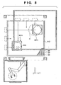
- Fig. 8 is a view showing a stage device in the exposure apparatus disclosed in Japanese Patent Laid-Open No. 2001-217183.
- reference symbol PL denotes a projection optical system
- ALG an alignment optical system.
- a stator 112 as a base has a measurement (alignment) region and exposure region.
- Two movable stages (WST1 and WST2) can move in the measurement region and exposure region independently of each other. In this exposure system, exposure and alignment measurement can be performed simultaneously, so that the throughput can be improved.
- the plane motor has a magnet group (not shown) arrayed on the lower surfaces of the movable stages (WST1 and WST2) and a coil group 98 arrayed in a matrix in the stator 112.
- the Lorentz force generated by the mutual operation of the magnetic fluxes of the magnet group and a current flowing through the coil group can move the movable stages (WST1 and WST2) relative to the stator 112.
- Fig. 7 shows the coil cooling structure of a plane motor disclosed in Japanese Patent Laid-Open No. 2001-175434.
- the coil group of the plane motor stator is sealed by a stator main body 32.
- a refrigerant is supplied from 88A (88B) and discharged from 92A (92B) to cool the coil group in the stator.
- stage operation for performing alignment measurement and stage operation for performing exposure are often different from each other.
- scanning must be performed for every shot of the exposure target.
- the stage moves uniformly to a certain degree through the entire region.
- the movement required of the stage varies depending on the accuracy to be obtained and a measuring method. Therefore, usually, the energization amount for the coil group arranged in the exposure region and that for the coil group arranged in the measurement region are different, and naturally the heat values of the two coil groups are expected to be different.
- the alignment measurement assume that a scheme that does not measure the entire wafer but measures only a certain representative point is employed.
- the movement of the stage required in the alignment measurement may be smaller than that required in the exposure region, and the energization amount and energization time of the coils are accordingly smaller than those for the coils in the exposure region. Therefore, the heat amount of the coil group in the measurement region becomes smaller than that in the exposure region. In fine, heat generation of the coil group in the stator largely differs between the two regions.
- the flow rate of the refrigerant flowing through a refrigerant pipe 89A (89B) of Fig. 7 is set such that the temperature of the refrigerant becomes equal to or less than an allowable temperature with respect to a coil with the largest heat generation.
- Embodiments of the present invention seek to efficiently remove, in a stage device having different process regions, heat generated by driving of a movable element having an object thereon.
- a stage device for driving a movable element, mounted with an object thereon, by using a plane motor comprising a stator unit having a coil group, and the movable element which moves on the stator unit, the stator unit comprising a first region where the object is to be subjected to a first process, and a second region where the object is to be subjected to a second process, wherein the coil group in the stator unit is temperature-controlled independently between the first and second regions.
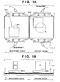
- Figs. 1A and 1B show a stage device according to the first embodiment.
- Fig. 1A is a view of the stage device seen from above
- Fig. 1B is a sectional view of the stage device seen from the horizontal direction.
- the stage device is divided into an exposure region and measurement region.
- An exposure optical system PL is arranged in the exposure region, and a measurement optical system ALG for alignment measurement is arranged in the measurement region.
- two movable stages can perform exposure operation and measurement operation in the corresponding regions.
- the movable stages WST1 and WST2 can be swapped between the exposure region and measurement region.
- the movable stage WST2 where wafer measurement operation has been finished swaps regions with the movable stage WST1 where exposure has been finished.
- the movable stage WST2 continuously starts exposure operation.
- the movable stage WST1 transfers an exposed wafer to a wafer transport system (not shown) and receives a new wafer to start alignment operation.
- Magnet groups (not shown) are arranged on the lower surfaces of the plate-like top plates of the movable stages WST1 and WST2, respectively.
- the stator units 3 facing the movable stages include coil groups 4 and 5, each formed of a large number of layers of coil arrays, and cooling jackets 6 and 7 which seal the coil groups 4 and 5.
- the Lorentz force generated by the interaction of the magnet groups of the movable stages and a current supplied to the coil groups moves the movable stages WST1 and WST2 with respect to the stator units 3.
- a refrigerant such as temperature-controlled pure water or an inert refrigerant flows through the cooling jackets 6 and 7 to be able to cool the coils directly.
- the coils may be cooled by providing cooling pipes among the coils.
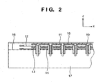
- Fig. 2 is an enlarged view of part of the coil group 4 or 5 in the corresponding stator unit 3.
- the coil group has a large number of layers of coil arrays in the vertical direction.
- a coil array 11 at the first layer from the top is a coil array that contributes to driving in an X-axis direction and ⁇ z direction (rotational direction about the Z-axis).
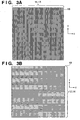
- the coil array 11 is formed by arranging a plurality of coils 18, having straight portions elongated in the Y-axis direction as shown in Fig. 3A, in the X-axis direction.
- a coil array 12 at the second layer from the top is a coil array that contributes to driving in a Y-axis direction and the ⁇ z direction.
- the coil array 12 is formed by arranging a plurality of coils 19, having straight portions elongated in the X-axis direction as shown in Fig. 3B, in the Y-axis direction.
- a coil array 13 at the third layer is a coil array that contributes to driving in a Z-axis direction and ⁇ y direction (rotational direction about the Y-axis).
- the coil array 13 is formed as shown in Fig. 3A.
- a coil array 14 at the fourth layer is a coil array that contributes to driving in the Z-axis direction and an ⁇ x direction (rotational direction about the X-axis).
- the coil array 14 is formed as shown in Fig. 4.
- the four layers of coil arrays can drive the movable stages in 6-axis directions.
- the arrangement of the coil group is not limited to this. As shown in Fig. 8, coils may be arranged in a matrix. Furthermore, the plane motor suffices as far as its stator unit has a coil group serving as a heat generating portion.
- the respective coil arrays are supported on a base surface plate 17 through support members 10.
- the gaps among the coil arrays form refrigerant flow channels. More specifically, the upper and lower surfaces of the coils come into contact with the circulating refrigerant so that they can be cooled directly.
- the coil group is cooled in this manner by circulating the refrigerant in the cooling jacket that surrounds the coil group, heat generated by the coils is removed quickly to prevent excessive temperature rise of the coils and temperature rise of the stator unit.
- the cooling jackets 6 and 7 are provided to the exposure region and measurement region independently of each other, and can optimally cool the corresponding regions independently of each other. If all the stators of a plane motor are cooled collectively as in the prior art, the entire cooling efficiency is poor, and the refrigerant temperature controlling unit, refrigerant circulating unit, and the like may become bulky.
- the respective regions can be cooled (e.g., flow rate of the refrigerant, temperature, and the type of the refrigerant) optimally for the movement of the stages. Then, an increase in the cooling efficiency can be expected, and units related to temperature control can be made compact.
- the cooling amount (the flow rate of the refrigerant, the temperature of the refrigerant, and the type of the refrigerant) is adjusted for a coil with the largest heat generation.
- the cooling amount is set to a value for the coil with the largest heat generation among all the coils.
- the stages move in the measurement region and exposure region largely differently from each other, and accordingly the heat generation amount of the coils is largely different between the measurement region and exposure region.
- the stage in the exposure region moves actively while the stage in the measurement stage does not move very actively so much as a stage because of wafer transfer or the like. Then, only the coil group in the exposure region generates heat largely, and the coil group in the measurement region rarely generates heat.
- the refrigerant in a cooling amount for the coils in the exposure region is supplied to the entire cooling jacket, so that an excessively large amount of refrigerant flows to the coil group in the measurement region wastefully.
- an excessively large flow rate of the refrigerant is required for all the stators.
- the cooling efficiency (the removing rate of heat generated by the coils to the flow rate of the refrigerant) decreases, and the units concerning temperature control become bulky.
- the measurement region and exposure region can be cooled independently of each other. More specifically, as the stages in the measurement region and exposure region move largely differently, cooling of the respective regions is optimized independently to increase the cooling efficiency as a whole. Cooling optimization includes, e.g., a change in at least one of the flow rate of the refrigerant, the temperature, and the type of the refrigerant between the measurement region and exposure region.
- the flowing direction of the refrigerant can also be changed.
- the refrigerant can be supplied into each region from the vicinity of a coil with the largest heat generation, so that optimal cooling can be performed.
- the above example mainly aims at optimizing cooling in the measurement region and exposure region independently.
- the cooling method (the flow rate of the refrigerant, the temperature, the type of the refrigerant, and the like) need not be changed between the measurement region and exposure region.
- stator units 3 appear to be provided to the measurement region and exposure region independently.
- the stator units themselves may be independent for the respective regions or be integral throughout the respective regions. It suffices as far as the interiors of the cooling jackets 6 and 7 can be temperature-controlled independently of each other.
- the minimum size of the stator unit of the plane motor is substantially determined by the wafer size.
- the necessary stroke of the movable stage in each of the measurement region and exposure region is about 400 mm (distance necessary for movement through the entire wafer region + distance necessary for the acceleration/deceleration region of the stage).
- the stator unit is assumed to require a size of 700 mm (300 mm as wafer size + 400 mm for stroke) or more at the minimum.
- the size of a stator unit including the measurement region and exposure region is at a minimum of 700 mm (X direction in Fig. 8) x 1,400 mm (Y direction in Fig. 8).
- the size of the stator unit tends to become larger due to various factors. If the stator unit having this size is to be fabricated as one integral unit, the necessary material may be difficult to obtain and the degree of freedom of machining may be limited by the limitations of the machine tool highly likely. Accordingly, the cost may be expected to increase. That is, if a measurement region and exposure region are provided independently of each other, the size of the stator may increase to cause difficulties in the manufacture.
- each fabrication size becomes half.
- an exposure region unit and fabrication of a measurement region unit can be fabricated simultaneously, so that the fabrication lead time can also be decreased.
- a countermeasure need be taken only for a unit where a trouble occurs.
- the maintenance need only be performed often on a small scale.
- stage device using a plane motor In a stage device provided with separate linear motors to drive respective stages for the exposure region and measurement region as well, to temperature-control the respective driving means independently of each other is effective in terms of the cooling efficiency. Note that the stage device using a plane motor is effective because the exposure region and measurement region can be cooled independently of each other with a simple structure and the heat generation amount of the coils is large.
- Fig. 4 shows an exposure apparatus for semiconductor device manufacture which uses a stage device similar to that described above as a wafer stage.
- This exposure apparatus is used to manufacture devices having fine patterns, e.g., a semiconductor device such as a semiconductor integrated circuit, a micromachine, and a thin-film magnetic head.
- Exposure light (this is a generic term for visible light, ultraviolet light, EUV light, X-rays, an electron beam, a charged particle beam, or the like) serving as an exposure energy from an illumination system unit 501 through a reticle as an original irradiates a semiconductor wafer W as a substrate through a projection lens 503 (this is a generic term for a dioptric lens, reflecting lens, cata-dioptric lens system, charged particle lens, or the like) serving as a projecting system to form a desired pattern on a substrate mounted on a wafer stage 504. As the wavelength of the exposure light becomes short, the exposure apparatus requires exposure in a vacuum atmosphere.
- a wafer (object) as a substrate is held on a chuck mounted on the wafer stage 504.
- the pattern of the reticle as the original mounted on a reticle stage 502 is transferred onto the respective regions on the wafer by the illumination system unit 501 in accordance with step & repeat or step & scan.
- the stage device described above is used as the wafer stage 504.
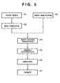
- Fig. 5 is a flowchart showing the flow of the entire semiconductor device manufacturing process.
- step 1 circuit design
- step 2 mask fabrication
- a mask is fabricated on the basis of the designed circuit pattern.
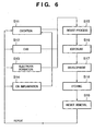
- the wafer process of the above step 4 includes the following steps (Fig. 6), i.e., an oxidation step of oxidizing the surface of the wafer, a CVD step of forming an insulating film on the wafer surface, an electrode formation step of forming an electrode on the wafer by deposition, an ion implantation step of implanting ions in the wafer, a resist process step of applying a photosensitive agent to the wafer, an exposure step of transferring the circuit pattern to the wafer after the resist process step by the exposure apparatus described above, a developing step of developing the wafer exposed in the exposure step, an etching step of removing portions other than the resist image developed in the developing step, and a resist removal step of removing any unnecessary resist after etching. These steps are repeated to form multiple circuit patterns on the wafer.
Landscapes
- Engineering & Computer Science (AREA)
- Physics & Mathematics (AREA)
- General Engineering & Computer Science (AREA)
- General Physics & Mathematics (AREA)
- Health & Medical Sciences (AREA)
- Life Sciences & Earth Sciences (AREA)
- Atmospheric Sciences (AREA)
- Environmental & Geological Engineering (AREA)
- Epidemiology (AREA)
- Public Health (AREA)
- Toxicology (AREA)
- Mechanical Engineering (AREA)
- Architecture (AREA)
- Materials Engineering (AREA)
- Wood Science & Technology (AREA)
- Chemical & Material Sciences (AREA)
- Civil Engineering (AREA)
- Structural Engineering (AREA)
- Exposure And Positioning Against Photoresist Photosensitive Materials (AREA)
- Exposure Of Semiconductors, Excluding Electron Or Ion Beam Exposure (AREA)
- Linear Motors (AREA)
Abstract
Description
the present invention, there is provided a stage device for driving a movable element, mounted with an object thereon, by using a plane motor, comprising a stator unit having a coil group, and the movable element which moves on the stator unit, the stator unit comprising a first region where the object is to be subjected to a first process, and a second region where the object is to be subjected to a second process, wherein the coil group in the stator unit is temperature-controlled independently between the first and second regions.
device having different process regions, heat generated by driving of a movable object mounted with an object thereon can be removed more efficiently.
Claims (12)
- A stage device for driving a movable element, mounted with an object thereon, by using a plane motor, comprising:said stator unit comprising:(i) a stator unit having a coil group; and(ii) said movable element which moves on said stator unit,wherein said coil group in said stator unit is temperature-controlled independently between said first and second regions.(a) a first region where the object is to be subjected to a first process; and(b) a second region where the object is to be subjected to a second process,
- The device according to claim 1, wherein
said stator unit has a cooling jacket which surrounds said coil group, and
said coil group is cooled by supplying a refrigerant into said cooling jacket. - The device according to claim 2, wherein the refrigerant flows in different directions between said first and second regions.
- The device according to claims 2 or 3, wherein a cooling amount of the refrigerant that cools said coil group differs between said first and second regions.
- The device according to claim 4, wherein at least one of a flow rate, temperature, and medium of the refrigerant that cools said coil group differs between said first and second regions.
- The device according to any one of claims 1 to 5, wherein said stator unit is divided between said first and second regions.
- The device according to any one of claims 1 to 6, wherein said movable element includes two movable elements, said two movable elements being capable of swapped between said first and second regions, by using the plane motor.
- The device according to any one of claims 1 to 7, wherein said movable element has a magnet group on a surface thereof which opposes said stator unit, said magnet group serving to generate a force with respect to said coil group of said stator unit.
- An exposure apparatus for positioning a substrate by using a stage device according to any one of claims 1 to 8, wherein
the first process comprises a process of exposing the substrate, and
the second process comprises a process of measuring a position of the substrate. - An exposure apparatus having an exposure region to expose a substrate and a measurement region to measure a position of the substrate, comprising:wherein said first and second driving means are temperature-controlled independently of each other.first driving means for driving in said exposure region a movable element mounted with the substrate thereon; andsecond driving means for driving said movable element in said measurement region,
- A device manufacturing method which has a step of exposing a substrate by using an exposure apparatus according to claims 9 or 10, a step of developing the exposed substrate, and one or more further steps for using all or part of the developed substrate to make an article.
- A stage arrangement for carrying a mask or a substrate in exposure apparatus for exposing a substrate with a pattern, comprising:characterised in thata stage;drive means for driving the stage; andcooling means for cooling the drive means,
the cooling means is arranged so that it can be used to cool different parts of the drive means independently of each other.
Applications Claiming Priority (2)
| Application Number | Priority Date | Filing Date | Title |
|---|---|---|---|
| JP2004087078 | 2004-03-24 | ||
| JP2004087078A JP4418699B2 (en) | 2004-03-24 | 2004-03-24 | Exposure equipment |
Publications (2)
| Publication Number | Publication Date |
|---|---|
| EP1580604A2 true EP1580604A2 (en) | 2005-09-28 |
| EP1580604A3 EP1580604A3 (en) | 2009-10-28 |
Family
ID=34858434
Family Applications (1)
| Application Number | Title | Priority Date | Filing Date |
|---|---|---|---|
| EP05251631A Withdrawn EP1580604A3 (en) | 2004-03-24 | 2005-03-17 | Stage device and exposure apparatus |
Country Status (6)
| Country | Link |
|---|---|
| US (2) | US7282820B2 (en) |
| EP (1) | EP1580604A3 (en) |
| JP (1) | JP4418699B2 (en) |
| KR (1) | KR100715784B1 (en) |
| CN (1) | CN1673872A (en) |
| TW (1) | TWI274376B (en) |
Cited By (2)
| Publication number | Priority date | Publication date | Assignee | Title |
|---|---|---|---|---|
| CN102854752A (en) * | 2011-05-27 | 2013-01-02 | 恩斯克科技有限公司 | Proximity exposure device |
| CN104638983B (en) * | 2013-11-14 | 2017-04-26 | 北京环境特性研究所 | Small magnetic levitation stabilization platform |
Families Citing this family (14)
| Publication number | Priority date | Publication date | Assignee | Title |
|---|---|---|---|---|
| JP4418699B2 (en) * | 2004-03-24 | 2010-02-17 | キヤノン株式会社 | Exposure equipment |
| JP2006287014A (en) * | 2005-04-01 | 2006-10-19 | Canon Inc | Positioning device and linear motor |
| JP4781049B2 (en) * | 2005-08-30 | 2011-09-28 | キヤノン株式会社 | Exposure apparatus and device manufacturing method |
| KR101323565B1 (en) * | 2006-01-19 | 2013-10-29 | 가부시키가이샤 니콘 | Moving body drive method, moving body drive system, pattern formation method, pattern formation device, exposure method, exposure device, and device fabrication method |
| TWI454859B (en) * | 2006-03-30 | 2014-10-01 | 尼康股份有限公司 | Mobile device, exposure device and exposure method, and component manufacturing method |
| JP4315455B2 (en) | 2006-04-04 | 2009-08-19 | キヤノン株式会社 | Exposure apparatus and device manufacturing method |
| JP2007312516A (en) * | 2006-05-18 | 2007-11-29 | Canon Inc | Drive apparatus, exposure apparatus, and device manufacturing method |
| DE102006039368A1 (en) * | 2006-08-22 | 2008-03-13 | Siemens Ag | Electric motor with self-cooling |
| TWI547771B (en) * | 2006-08-31 | 2016-09-01 | 尼康股份有限公司 | Mobile body drive system and moving body driving method, pattern forming apparatus and method, exposure apparatus and method, component manufacturing method, and method of determining |
| US7592760B2 (en) * | 2006-09-11 | 2009-09-22 | Asml Netherlands B.V. | Lithographic apparatus and device manufacturing method |
| JP5137879B2 (en) * | 2009-03-04 | 2013-02-06 | キヤノン株式会社 | Exposure apparatus and device manufacturing method |
| JP5918965B2 (en) | 2011-10-25 | 2016-05-18 | キヤノン株式会社 | Processing machine system and processing machine arrangement method |
| US9778579B2 (en) * | 2011-11-10 | 2017-10-03 | Nikon Corporation | System and method for controlling a temperature of a reaction assembly |
| US10268128B2 (en) | 2015-07-08 | 2019-04-23 | Asml Netherlands B.V. | Lithographic apparatus |
Family Cites Families (35)
| Publication number | Priority date | Publication date | Assignee | Title |
|---|---|---|---|---|
| US5231291A (en) * | 1989-08-01 | 1993-07-27 | Canon Kabushiki Kaisha | Wafer table and exposure apparatus with the same |
| JP3363662B2 (en) * | 1994-05-19 | 2003-01-08 | キヤノン株式会社 | Scanning stage apparatus and exposure apparatus using the same |
| JP3484684B2 (en) * | 1994-11-01 | 2004-01-06 | 株式会社ニコン | Stage apparatus and scanning type exposure apparatus |
| JP3613291B2 (en) * | 1995-03-08 | 2005-01-26 | 株式会社ニコン | Exposure equipment |
| JP3709896B2 (en) * | 1995-06-15 | 2005-10-26 | 株式会社ニコン | Stage equipment |
| US5959732A (en) * | 1996-04-10 | 1999-09-28 | Nikon Corporation | Stage apparatus and a stage control method |
| JPH09320934A (en) * | 1996-05-28 | 1997-12-12 | Nikon Corp | Stage device |
| JPH09308218A (en) * | 1996-05-10 | 1997-11-28 | Canon Inc | Linear motor and stage device and exposure device using the same |
| JP3661291B2 (en) * | 1996-08-01 | 2005-06-15 | 株式会社ニコン | Exposure equipment |
| EP0827186A3 (en) * | 1996-08-29 | 1999-12-15 | Tokyo Electron Limited | Substrate treatment system |
| JPH11307430A (en) | 1998-04-23 | 1999-11-05 | Canon Inc | Exposure apparatus, device manufacturing method, and driving apparatus |
| JP4088728B2 (en) * | 1998-07-09 | 2008-05-21 | 株式会社ニコン | Planar motor device, driving device and exposure device |
| JP2001175434A (en) | 1999-10-14 | 2001-06-29 | Xerox Corp | Method for operating digital printing device |
| JP2001217183A (en) | 2000-02-04 | 2001-08-10 | Nikon Corp | Motor apparatus, stage apparatus, exposure apparatus, and device manufacturing method |
| TW588222B (en) * | 2000-02-10 | 2004-05-21 | Asml Netherlands Bv | Cooling of voice coil motors in lithographic projection apparatus |
| JP3870002B2 (en) | 2000-04-07 | 2007-01-17 | キヤノン株式会社 | Exposure equipment |
| JP4383626B2 (en) | 2000-04-13 | 2009-12-16 | キヤノン株式会社 | Positioning apparatus and exposure apparatus |
| US6842248B1 (en) * | 2000-11-28 | 2005-01-11 | Nikon Corporation | System and method for calibrating mirrors of a stage assembly |
| JP4724297B2 (en) | 2000-12-26 | 2011-07-13 | キヤノン株式会社 | Exposure apparatus and device manufacturing method |
| US6570273B2 (en) * | 2001-01-08 | 2003-05-27 | Nikon Corporation | Electric linear motor |
| JP2002280283A (en) | 2001-03-16 | 2002-09-27 | Canon Inc | Substrate processing equipment |
| JP3768825B2 (en) * | 2001-03-29 | 2006-04-19 | キヤノン株式会社 | Electromagnetic actuator, linear motor, exposure apparatus, semiconductor device manufacturing method, semiconductor manufacturing factory, and exposure apparatus maintenance method |
| TW552805B (en) * | 2001-05-17 | 2003-09-11 | Koninkl Philips Electronics Nv | Output stabilization for a laser matrix |
| EP1276016B1 (en) | 2001-07-09 | 2009-06-10 | Canon Kabushiki Kaisha | Exposure apparatus |
| JP4745556B2 (en) | 2001-08-20 | 2011-08-10 | キヤノン株式会社 | Positioning apparatus, exposure apparatus, and device manufacturing method |
| JP2004146492A (en) | 2002-10-23 | 2004-05-20 | Canon Inc | EUV exposure equipment |
| TW200305927A (en) * | 2002-03-22 | 2003-11-01 | Nippon Kogaku Kk | Exposure apparatus, exposure method and manufacturing method of device |
| JP2004134566A (en) * | 2002-10-10 | 2004-04-30 | Canon Inc | Device manufacturing equipment |
| JP4266713B2 (en) | 2003-06-03 | 2009-05-20 | キヤノン株式会社 | Positioning apparatus and exposure apparatus |
| JP3748559B2 (en) | 2003-06-30 | 2006-02-22 | キヤノン株式会社 | Stage apparatus, exposure apparatus, charged beam drawing apparatus, device manufacturing method, substrate potential measuring method, and electrostatic chuck |
| JP3894562B2 (en) | 2003-10-01 | 2007-03-22 | キヤノン株式会社 | Substrate adsorption apparatus, exposure apparatus, and device manufacturing method |
| JP3814598B2 (en) | 2003-10-02 | 2006-08-30 | キヤノン株式会社 | Temperature adjustment apparatus, exposure apparatus, and device manufacturing method |
| JP4418699B2 (en) * | 2004-03-24 | 2010-02-17 | キヤノン株式会社 | Exposure equipment |
| US7959780B2 (en) * | 2004-07-26 | 2011-06-14 | Emporia Capital Funding Llc | Textured ion exchange membranes |
| JP4315455B2 (en) * | 2006-04-04 | 2009-08-19 | キヤノン株式会社 | Exposure apparatus and device manufacturing method |
-
2004
- 2004-03-24 JP JP2004087078A patent/JP4418699B2/en not_active Expired - Fee Related
-
2005
- 2005-03-09 US US11/074,642 patent/US7282820B2/en not_active Expired - Fee Related
- 2005-03-11 TW TW094107541A patent/TWI274376B/en not_active IP Right Cessation
- 2005-03-17 EP EP05251631A patent/EP1580604A3/en not_active Withdrawn
- 2005-03-22 CN CNA2005100548854A patent/CN1673872A/en active Pending
- 2005-03-24 KR KR1020050024323A patent/KR100715784B1/en not_active Expired - Fee Related
-
2007
- 2007-10-12 US US11/871,328 patent/US20080036981A1/en not_active Abandoned
Cited By (2)
| Publication number | Priority date | Publication date | Assignee | Title |
|---|---|---|---|---|
| CN102854752A (en) * | 2011-05-27 | 2013-01-02 | 恩斯克科技有限公司 | Proximity exposure device |
| CN104638983B (en) * | 2013-11-14 | 2017-04-26 | 北京环境特性研究所 | Small magnetic levitation stabilization platform |
Also Published As
| Publication number | Publication date |
|---|---|
| EP1580604A3 (en) | 2009-10-28 |
| KR20060044654A (en) | 2006-05-16 |
| TWI274376B (en) | 2007-02-21 |
| CN1673872A (en) | 2005-09-28 |
| US7282820B2 (en) | 2007-10-16 |
| US20050212361A1 (en) | 2005-09-29 |
| US20080036981A1 (en) | 2008-02-14 |
| TW200532770A (en) | 2005-10-01 |
| JP4418699B2 (en) | 2010-02-17 |
| KR100715784B1 (en) | 2007-05-10 |
| JP2005277030A (en) | 2005-10-06 |
Similar Documents
| Publication | Publication Date | Title |
|---|---|---|
| US20080036981A1 (en) | Stage Device And Exposure Apparatus | |
| EP2998983B1 (en) | Stage apparatus, exposure apparatus and device fabricating method | |
| US6590355B1 (en) | Linear motor device, stage device, and exposure apparatus | |
| KR102278378B1 (en) | Motor assembly, lithographic apparatus and device manufacturing method | |
| KR101716267B1 (en) | Lithographic apparatus and device manufacturing method | |
| US7282874B2 (en) | Alignment apparatus, exposure apparatus, and device manufacturing method | |
| EP1788694A1 (en) | Planar motor equipment, stage equipment, exposure equipment and device manufacturing method | |
| KR20170133526A (en) | Exposure apparatus and device manufacturing method | |
| JP2000201471A (en) | Actuators and transducers | |
| JP2004146492A (en) | EUV exposure equipment | |
| JP2000331929A (en) | Lithographic projection apparatus and method | |
| JP4566697B2 (en) | Positioning apparatus, exposure apparatus using the same, and device manufacturing method | |
| JP2005295762A (en) | Stage apparatus and exposure apparatus | |
| US7408276B2 (en) | Plane motor device with surrounding member surrounding coil unit and with cooling channel provided within surrounding member | |
| US20080079953A1 (en) | Alignment apparatus, exposure apparatus, and device manufacturing method using exposure apparatus | |
| JP2008235470A (en) | Planar motor apparatus, stage apparatus, exposure apparatus, and device manufacturing method | |
| US7239051B2 (en) | Driving apparatus and exposure apparatus | |
| US7245092B2 (en) | Alignment stage apparatus, exposure apparatus, and semiconductor device manufacturing method | |
| US7391495B2 (en) | Stage apparatus, exposure system using the same, and device manufacturing method | |
| JP2010200452A (en) | Motor device, stage device, and aligner | |
| JP2006156554A (en) | STAGE APPARATUS, EXPOSURE APPARATUS USING SAME, AND DEVICE MANUFACTURING METHOD | |
| JP3944198B2 (en) | Stage apparatus, exposure apparatus, and device manufacturing method | |
| JP2004335677A (en) | Flat motor device | |
| HK1218185B (en) | Stage apparatus, exposure apparatus and device fabricating method | |
| HK1124693A (en) | Pattern formation method and pattern formation apparatus, exposure metho and exposure apparatus, and device manufacturing method |
Legal Events
| Date | Code | Title | Description |
|---|---|---|---|
| PUAI | Public reference made under article 153(3) epc to a published international application that has entered the european phase |
Free format text: ORIGINAL CODE: 0009012 |
|
| AK | Designated contracting states |
Kind code of ref document: A2 Designated state(s): AT BE BG CH CY CZ DE DK EE ES FI FR GB GR HU IE IS IT LI LT LU MC NL PL PT RO SE SI SK TR |
|
| AX | Request for extension of the european patent |
Extension state: AL BA HR LV MK YU |
|
| PUAL | Search report despatched |
Free format text: ORIGINAL CODE: 0009013 |
|
| AK | Designated contracting states |
Kind code of ref document: A3 Designated state(s): AT BE BG CH CY CZ DE DK EE ES FI FR GB GR HU IE IS IT LI LT LU MC NL PL PT RO SE SI SK TR |
|
| AX | Request for extension of the european patent |
Extension state: AL BA HR LV MK YU |
|
| STAA | Information on the status of an ep patent application or granted ep patent |
Free format text: STATUS: THE APPLICATION HAS BEEN WITHDRAWN |
|
| 18W | Application withdrawn |
Effective date: 20100325 |