EP1577943A2 - Semiconductor substrate, manufacturing method therefor, and semiconductor device - Google Patents
Semiconductor substrate, manufacturing method therefor, and semiconductor device Download PDFInfo
- Publication number
- EP1577943A2 EP1577943A2 EP04011379A EP04011379A EP1577943A2 EP 1577943 A2 EP1577943 A2 EP 1577943A2 EP 04011379 A EP04011379 A EP 04011379A EP 04011379 A EP04011379 A EP 04011379A EP 1577943 A2 EP1577943 A2 EP 1577943A2
- Authority
- EP
- European Patent Office
- Prior art keywords
- layer
- silicon
- substrate
- strained
- semiconductor
- Prior art date
- Legal status (The legal status is an assumption and is not a legal conclusion. Google has not performed a legal analysis and makes no representation as to the accuracy of the status listed.)
- Withdrawn
Links
Images

Classifications
-
- H—ELECTRICITY
- H10—SEMICONDUCTOR DEVICES; ELECTRIC SOLID-STATE DEVICES NOT OTHERWISE PROVIDED FOR
- H10D—INORGANIC ELECTRIC SEMICONDUCTOR DEVICES
- H10D30/00—Field-effect transistors [FET]
- H10D30/60—Insulated-gate field-effect transistors [IGFET]
- H10D30/67—Thin-film transistors [TFT]
- H10D30/674—Thin-film transistors [TFT] characterised by the active materials
- H10D30/6741—Group IV materials, e.g. germanium or silicon carbide
- H10D30/6748—Group IV materials, e.g. germanium or silicon carbide having a multilayer structure or superlattice structure
-
- H—ELECTRICITY
- H10—SEMICONDUCTOR DEVICES; ELECTRIC SOLID-STATE DEVICES NOT OTHERWISE PROVIDED FOR
- H10D—INORGANIC ELECTRIC SEMICONDUCTOR DEVICES
- H10D84/00—Integrated devices formed in or on semiconductor substrates that comprise only semiconducting layers, e.g. on Si wafers or on GaAs-on-Si wafers
- H10D84/01—Manufacture or treatment
- H10D84/0123—Integrating together multiple components covered by H10D12/00 or H10D30/00, e.g. integrating multiple IGBTs
- H10D84/0126—Integrating together multiple components covered by H10D12/00 or H10D30/00, e.g. integrating multiple IGBTs the components including insulated gates, e.g. IGFETs
- H10D84/0165—Integrating together multiple components covered by H10D12/00 or H10D30/00, e.g. integrating multiple IGBTs the components including insulated gates, e.g. IGFETs the components including complementary IGFETs, e.g. CMOS devices
- H10D84/0167—Manufacturing their channels
-
- H—ELECTRICITY
- H10—SEMICONDUCTOR DEVICES; ELECTRIC SOLID-STATE DEVICES NOT OTHERWISE PROVIDED FOR
- H10D—INORGANIC ELECTRIC SEMICONDUCTOR DEVICES
- H10D84/00—Integrated devices formed in or on semiconductor substrates that comprise only semiconducting layers, e.g. on Si wafers or on GaAs-on-Si wafers
- H10D84/01—Manufacture or treatment
- H10D84/0123—Integrating together multiple components covered by H10D12/00 or H10D30/00, e.g. integrating multiple IGBTs
- H10D84/0126—Integrating together multiple components covered by H10D12/00 or H10D30/00, e.g. integrating multiple IGBTs the components including insulated gates, e.g. IGFETs
- H10D84/0165—Integrating together multiple components covered by H10D12/00 or H10D30/00, e.g. integrating multiple IGBTs the components including insulated gates, e.g. IGFETs the components including complementary IGFETs, e.g. CMOS devices
- H10D84/0188—Manufacturing their isolation regions
-
- H—ELECTRICITY
- H10—SEMICONDUCTOR DEVICES; ELECTRIC SOLID-STATE DEVICES NOT OTHERWISE PROVIDED FOR
- H10D—INORGANIC ELECTRIC SEMICONDUCTOR DEVICES
- H10D84/00—Integrated devices formed in or on semiconductor substrates that comprise only semiconducting layers, e.g. on Si wafers or on GaAs-on-Si wafers
- H10D84/01—Manufacture or treatment
- H10D84/02—Manufacture or treatment characterised by using material-based technologies
- H10D84/03—Manufacture or treatment characterised by using material-based technologies using Group IV technology, e.g. silicon technology or silicon-carbide [SiC] technology
- H10D84/038—Manufacture or treatment characterised by using material-based technologies using Group IV technology, e.g. silicon technology or silicon-carbide [SiC] technology using silicon technology, e.g. SiGe
-
- H—ELECTRICITY
- H10—SEMICONDUCTOR DEVICES; ELECTRIC SOLID-STATE DEVICES NOT OTHERWISE PROVIDED FOR
- H10D—INORGANIC ELECTRIC SEMICONDUCTOR DEVICES
- H10D84/00—Integrated devices formed in or on semiconductor substrates that comprise only semiconducting layers, e.g. on Si wafers or on GaAs-on-Si wafers
- H10D84/80—Integrated devices formed in or on semiconductor substrates that comprise only semiconducting layers, e.g. on Si wafers or on GaAs-on-Si wafers characterised by the integration of at least one component covered by groups H10D12/00 or H10D30/00, e.g. integration of IGFETs
- H10D84/82—Integrated devices formed in or on semiconductor substrates that comprise only semiconducting layers, e.g. on Si wafers or on GaAs-on-Si wafers characterised by the integration of at least one component covered by groups H10D12/00 or H10D30/00, e.g. integration of IGFETs of only field-effect components
- H10D84/83—Integrated devices formed in or on semiconductor substrates that comprise only semiconducting layers, e.g. on Si wafers or on GaAs-on-Si wafers characterised by the integration of at least one component covered by groups H10D12/00 or H10D30/00, e.g. integration of IGFETs of only field-effect components of only insulated-gate FETs [IGFET]
- H10D84/85—Complementary IGFETs, e.g. CMOS
- H10D84/856—Complementary IGFETs, e.g. CMOS the complementary IGFETs having different architectures than each other, e.g. high-voltage and low-voltage CMOS
-
- H—ELECTRICITY
- H10—SEMICONDUCTOR DEVICES; ELECTRIC SOLID-STATE DEVICES NOT OTHERWISE PROVIDED FOR
- H10D—INORGANIC ELECTRIC SEMICONDUCTOR DEVICES
- H10D86/00—Integrated devices formed in or on insulating or conducting substrates, e.g. formed in silicon-on-insulator [SOI] substrates or on stainless steel or glass substrates
- H10D86/01—Manufacture or treatment
-
- H—ELECTRICITY
- H10—SEMICONDUCTOR DEVICES; ELECTRIC SOLID-STATE DEVICES NOT OTHERWISE PROVIDED FOR
- H10D—INORGANIC ELECTRIC SEMICONDUCTOR DEVICES
- H10D86/00—Integrated devices formed in or on insulating or conducting substrates, e.g. formed in silicon-on-insulator [SOI] substrates or on stainless steel or glass substrates
- H10D86/201—Integrated devices formed in or on insulating or conducting substrates, e.g. formed in silicon-on-insulator [SOI] substrates or on stainless steel or glass substrates the substrates comprising an insulating layer on a semiconductor body, e.g. SOI
Definitions
- the present invention relates to a semiconductor substrate, manufacturing method therefor, and semiconductor device and, more particularly, to a semiconductor substrate including, e.g., regions with different strained states in a surface layer, i.e., a strained semiconductor region and unstrained semiconductor region, a manufacturing method therefor, and a semiconductor device using the semiconductor substrate.
- the strained Si layer is defined as an Si layer whose lattice constant deviates from an original Si lattice constant owing to the stress.
- An Si layer without stress having an original Si lattice constant will be called as a relaxed Si layer, compared to the strained Si layer.
- silicon germanium (SiGe) silicon germanium to be described later, an SiGe layer with stress will be called a strained SiGe layer, and an SiGe layer without stress will be called as a relaxed SiGe layer.
- the operation speed of a semiconductor device can be increased when the device is formed using, e.g., a strained Si layer with tensile stress for a channel of an n-channel metal-oxide semiconductor field effect transistor (MOSFET: to be referred to as an nMOS hereinafter).
- MOSFET metal-oxide semiconductor field effect transistor
- a high-performance, advanced-function semiconductor device can be manufactured by embedding semiconductor devices with various functions on a strained Si substrate having a strained Si layer.
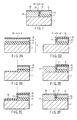
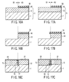
- FIGS. 18A and 18B An example of the substrate is shown in FIGS. 18A and 18B.
- This example employs a strained silicon on insulator (SOI) substrate 3 (FIG. 18A) having a thin strained Si layer 21 formed above a substrate 1 and a buried oxide film (BOX) layer 11 and relaxed SiGe layer 12 without stress which are sandwiched between the strained Si layer 21 and the Si substrate 1.
- SOI silicon on insulator
- BOX buried oxide film
- relaxed SiGe layer 12 without stress which are sandwiched between the strained Si layer 21 and the Si substrate 1.
- a relaxed Si region B having a relaxed Si layer 22 without stress is formed on part of the substrate surface while a strained Si region A having the strained Si layer 21 remains in the rest of the surface.
- the relaxed Si region B can be formed as follows. First, the entire surface is thermally oxidized to form an oxide film (SiO 2 film), and the strained Si layer 21 in the region B is exposed by patterning. In the region B, the Si substrate 1 is exposed by selectively removing the exposed strained Si layer 21, relaxed SiGe layer 12, and BOX layer 11. A relaxed Si layer 22 without stress is formed on the Si substrate 1 by selective epitaxial growth, then the SiO 2 film on the strained Si layer 21 surface is removed. In this manner, a semiconductor substrate having the strained Si region A whose surface is the strained Si layer 21 and the relaxed Si region B whose surface is the relaxed Si layer 22 without stress is formed, as shown in FIG. 18B.
- annealing at a relatively high temperature such as thermal oxidization or hydrogen annealing is generally performed before selective epitaxial growth.
- the annealing generates misfit dislocations near an interface between the strained Si layer 21 and the relaxed SiGe layer 12 due to the difference between their lattice constants, thereby relaxing the strain of the strained Si layer 21.
- Thermal oxidization of the thin strained Si layer 21 makes the layer 21 thinner, and also makes it difficult to control the thickness of the strained Si layer 21, exactly.
- Another example is a semiconductor substrate having a strained Si region A and relaxed Si region B by using a strained Si substrate 2, as a starting material, in which a strained Si layer 21 is formed on an SiGe buffer layer 31 on an Si substrate 1, as shown in FIG. 19A.
- a strained Si layer 21 is formed on an SiGe buffer layer 31 on an Si substrate 1, as shown in FIG. 19A.
- its Ge concentration is low in a portion close to the Si substrate 1 in order to suppress the generation of above-mentioned misfit dislocations, and gradually increases toward the surface.
- the relaxed Si region B is formed as follows. First, part of the strained Si layer 21 is covered with a mask, and the relaxed Si region B being formed an Si layer without stress is exposed. Then, the strained Si layer 21 and SiGe buffer layer 31 in the region B are selectively etched away to expose the surface of the unstrained Si substrate 1. The exposed surface is defined as the relaxed Si region B, as shown in FIG. 19B. In this structure, a step is formed between the strained Si region A on the SiGe buffer layer 31 and the relaxed Si region B from which the SiGe buffer layer 31 is removed.
- the SiGe buffer layer 31 is a so-called graded SiGe layer in which the Ge concentration in Si is not uniform in the direction of thickness, lower near the Si substrate 1, and gradually higher toward the surface.
- the SiGe buffer layer 31 is etched away, as described above.
- the selectivity in the etching between the SiGe buffer layer 31 and Si substrate 1 becomes low, failing to control the etching amount. Consequently, the etching uniformity in a wafer, between wafers and among lots becomes worse, and the level of the relaxed Si region B becomes nonuniform.
- the SiGe buffer layer 31 contains many misfit dislocations in order to relax the difference in lattice constant between the Si substrate 1 and the SiGe buffer layer 31.
- a deep semiconductor element e.g., a trench memory cell
- the trench may cross the misfit dislocation.
- the dislocation acts as a current leakage path, and the element characteristics is degraded by an increased leakage current.
- a semiconductor substrate In order to manufacture a semiconductor device with excellent desired characteristics, a semiconductor substrate must be obtained in which (1) the entire substrate is flat without any step between the strained Si region and the relaxed Si region, (2) the strained Si layer and relaxed Si layer, in which semiconductor elements are to be formed, are uniform in, for example, the thicknesses and impurity concentrations, and (3) lattice defects such as misfit dislocations do not exist in a trench formation region in the substrate.
- a semiconductor substrate comprises a support substrate, a first semiconductor region including a first silicon layer formed above the support substrate, a second semiconductor region including a strained second silicon layer formed above the support substrate, a surface of the second silicon layer being formed at substantially the same level as a surface of the first silicon layer, and an insulating film at an interface between the first semiconductor region and the second semiconductor region.
- a semiconductor device comprises a support substrate, a first semiconductor region including a second silicon layer formed on a first silicon layer above the support substrate, a second semiconductor region including a strained third silicon layer formed on a silicon germanium layer above the support substrate, a surface of the third silicon layer being formed at substantially the same level as a surface of the second silicon layer, an insulating film which is formed on an interface between the first semiconductor region and the second semiconductor region below an isolation insulator formed between the first semiconductor region and the second semiconductor region, a trench memory cell which is formed in the first semiconductor region, and a field effect transistor which is formed in the second semiconductor region.
- a semiconductor substrate manufacturing method for forming a first insulating film on a semiconductor substrate including a first semiconductor layer, patterning the first insulating film, removing part of the semiconductor substrate to form a recess, forming a second insulating film on an entire surface, removing the second insulating film from a bottom surface in the recess, forming a second semiconductor layer in the recess from a material different from a material of the first semiconductor layer, removing the first and second insulating films from a surface of the first semiconductor layer, and simultaneously forming a first silicon layer on the first semiconductor layer and a second silicon layer on the second semiconductor layer, a surface of the second silicon layer being substantially flush with a surface of the first silicon layer.
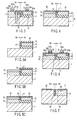
- the first embodiment uses, as a starting material, a substrate 4 (to be referred to as a silicon germanium on insulator (SGOI) substrate hereinafter) prepared by forming a relaxed SiGe layer 12 on a BOX layer 11 serving as an insulating layer on an Si substrate 1 serving as a support substrate.
- a semiconductor substrate according to the first embodiment has a strained Si region A1 including a strained Si layer 21 formed on the relaxed SiGe layer 12 by an epitaxial growth of Si, and a relaxed Si region B1 including a relaxed Si layer 22 without stress that is formed on a selectively epitaxially grown Si layer 15 at almost the same level as the strained Si layer 21. According to the feature of the semiconductor substrate, control of the film thickness of the strained Si layer 21 is facilitated at high quality.
- the strained state of the surface of the semiconductor substrate manufactured according to the first embodiment was evaluated by Raman spectroscopy analysis. It was confirmed that the strained Si layer 21 was formed on the relaxed SiGe layer 12 and the relaxed Si layer 22 without stress was formed on the epitaxial Si layer 15.
- an isolation IS in the semiconductor substrate in the strained Si region A1, for example, an nMOS having a source/drain SDa, gate insulator GIa, and gate electrode GEa is formed.
- the relaxed Si region B1 for example, a trench type dynamic random access memory (DRAM) cell having a source/drain SDb, gate insulator GIb, gate electrode GEb, and trench capacitor TC is formed.
- DRAM dynamic random access memory
- part of the SiN film 18 remains below the isolation IS at the interface between the strained Si region A1 and the relaxed Si region B1.
- the SiN film 18 has an effect of completely isolating elements.
- the operation of the semiconductor device was evaluated to confirm that the operation speed was higher and the leakage current of the memory cell was lower than those of a semiconductor device manufactured by a conventional technique.
- a semiconductor substrate can be manufactured in which both the strained Si region A1 having the strained Si layer 21 at the surface and the relaxed Si region B1 having the relaxed Si layer 22 without stress are formed at almost the same level.
- a higher-speed, higher-performance semiconductor device than a semiconductor device manufactured by a conventional method can be manufactured.
- the second embodiment is related to a semiconductor substrate preferable to manufacturing a complementary metal-oxide semiconductor (CMOS), based on the first embodiment. Similar to the first embodiment, as shown in FIG. 4, the second embodiment uses an SGOI 4, as a starting material, prepared by forming a relaxed SiGe layer 12 on a BOX layer 11 on an Si substrate 1.
- a semiconductor substrate according to the second embodiment has a strained Si region A1 including a strained Si layer 21 formed on the relaxed SiGe layer 12 on the BOX layer 11 by epitaxial growth of Si, and a relaxed Si region B2 including a relaxed Si layer 22 without stress that is formed on a strained SiGe layer 13 on a selectively epitaxially grown Si layer 15 at almost the same level as the strained Si layer 21. According to the feature of the semiconductor substrate, control of the film thicknesses of the strained Si layer 21 and relaxed Si layer 22 is facilitated at high quality.
- FIG. 5A is a sectional view identical to FIG. 2D. Manufacturing steps up to the step of FIG. 5A are the same as steps (1) to (4) in the first embodiment, and will be briefly explained.
- Formation of the epitaxial Si layer 22 on the strained SiGe layer 13 can also be prevented by performing epitaxial growth while covering the strained SiGe layer 13 with, e.g., an SiO 2 film.
- the strained state of the surface of the semiconductor substrate manufactured according to the second embodiment was evaluated by Raman spectroscopy analysis. It was confirmed that the strained Si layer 21 was formed on the relaxed SiGe layer 12 and the relaxed Si layer 22 without stress was formed on the strained SiGe layer 13 on the epitaxial Si layer 15.
- an isolation IS in the semiconductor substrate in the strained Si region A1, for example, an nMOS having a source/drain SDa, gate insulator GIa, and gate electrode GEa is formed.
- a pMOS having a source/drain SDb, gate insulator GIb, and gate electrode GEb is formed in the relaxed Si region B2.
- the pMOS is so manufactured as to form a channel in the strained SiGe layer 13.
- the SiO 2 film 17 and SiN film 18 partially remain below the isolation IS at the interface between the strained Si region A1 and the relaxed Si region B2.
- the SiO 2 film 17 and SiN film 18 have an effect of completely isolating elements.
- the switching speeds of both the nMOS and pMOS increased in comparison with a semiconductor device manufactured by a conventional technique.
- a semiconductor substrate can be manufactured in which both the strained Si region A1 having the strained Si layer 21 on the surface and the relaxed Si region B2 having the relaxed Si layer 22 without stress are formed at almost the same level.
- a higher-speed, higher-performance semiconductor device than a semiconductor device manufactured by a conventional method can be manufactured.
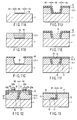
- the third embodiment adopts a substrate (to be referred to as a silicon-germanium on nothing (SGON) hereinafter) prepared by forming a relaxed SiGe layer above a cavity, instead of the SGOI substrate 4.
- the third embodiment forms an SGON structure by using an Si substrate 1 as a starting material.
- a semiconductor substrate according to the third embodiment has a strained Si region A2 including a strained Si layer 21 formed on a relaxed SiGe layer 12 having a cavity 33 by epitaxial growth of Si, and a relaxed Si region B3 including a relaxed Si layer 22 without stress that is formed on the Si substrate 1 at almost the same level as the strained Si layer 21.
- control of the film thickness of the strained Si layer 21 is facilitated at high quality.
- the third embodiment can reduce the number of manufacturing steps and the manufacturing cost in comparison with the first and second embodiments.
- the strained state of the surface of the semiconductor substrate manufactured according to the third embodiment was evaluated by Raman spectroscopy analysis. It was confirmed that the strained Si layer 21 was formed on the relaxed SiGe layer 12 and the relaxed Si layer 22 without stress was formed on the Si substrate 1.
- an isolation IS in the semiconductor substrate in the strained Si region A2, for example, an nMOS having a source/drain SDa, gate insulator GIa, and gate electrode GEa is formed.
- the relaxed Si region B3 for example, a trench DRAM cell having a source/drain SDb, gate insulator GIb, gate electrode GEb, and trench capacitor TC is formed.
- the SiO 2 film 17 and SiN film 18 partially remain below the isolation IS at the interface between the strained Si region A2 and the relaxed Si region B3.
- the SiO 2 film 17 and SiN film 18 have an effect of completely isolating elements.
- the operation of the semiconductor device was evaluated to confirm that the operation speed was higher and the leakage current of the memory cell was lower than those of a semiconductor device manufactured by a conventional technique.
- a semiconductor substrate can be manufactured in which both the strained Si region A2 having the strained Si layer 21 on the surface and the relaxed Si region B3 having the relaxed Si layer 22 without stress are formed at almost the same level.
- a higher-speed, higher-performance semiconductor device than a semiconductor device manufactured by a conventional method can be manufactured.
- the fourth embodiment concerns a substrate applied to a CMOS semiconductor device, similar to the second embodiment.
- the semiconductor substrate according to the fourth embodiment has a strained Si region A3 including a strained Si layer 21 that is epitaxially grown on a relaxed SiGe layer 12-2 on an Si substrate 1, and a relaxed Si region B2 including a relaxed Si layer 22 without stress that is epitaxially grown on a strained SiGe layer 13 on an Si layer 15 formed on the Si substrate 1.
- This semiconductor substrate therefore, has the strained Si region A3 and relaxed Si region B2 at almost the same level. According to the feature of the semiconductor substrate, control of the film thicknesses of the strained Si layer 21 and relaxed Si layer 22 is facilitated at high quality.
- SiGe layer is epitaxially grown to a thickness of, e.g., 200 nm on the entire surface to form SiGe layers 12-2 and 13.
- Epitaxial growth conditions of the SiGe layer are, e.g., 0.4 slm of SiH 2 Cl 2 , 0.2 slm of GeH 4 , a pressure of 10 Torr, and a temperature of 800°C.
- the SiGe layer 12-2 grown on the relaxed SiGe layer 12-1 is a relaxed SiGe layer
- the SiGe layer 13 grown on the epitaxial Si layer 15 is a strained SiGe layer.
- An Si layer is epitaxially grown to a thickness of, e.g., 20 nm on the entire surface to form Si layers 21 and 22.
- Epitaxial growth conditions are, e.g., 0.3 slm of SiH 2 Cl 2 in an H 2 carrier gas, a pressure of 10 Torr, and a temperature of 800°C. Accordingly, as shown in FIG. 11F, the strained Si layer 21 and the relaxed Si layer 22 without stress can be formed at almost the same level on the relaxed SiGe layers 12-2 and 12-1 over the strained SiGe layer 13 on the epitaxial Si layer 15, respectively.
- the strained state of the surface of the semiconductor substrate manufactured according to the fourth embodiment was evaluated by Raman spectroscopy analysis. It was confirmed that the strained Si layer 21 was formed on the relaxed SiGe layers 12-1 and 12-2 and the relaxed Si layer 22 without stress was formed on the strained SiGe layer 13 on the Si substrate 1.
- an isolation IS in the semiconductor substrate in the strained Si region A3, for example, an nMOS having a source/drain SDa, gate insulator GIa, and gate electrode GEa is formed.
- a pMOS having a source/drain SDb, gate insulator GIb, and gate electrode GEb is formed in the relaxed Si region B2.
- the pMOS is so manufactured as to form a channel in the strained SiGe layer 13.
- the SiO 2 film 17 and SiN film 18 partially remain below the isolation IS at the interface between the strained Si region A3 and the relaxed Si region B2.
- the SiO 2 film 17 and SiN film 18 have an effect of completely isolating elements.
- the switching speeds of both the nMOS and pMOS increased in comparison with a semiconductor device manufactured by a conventional technique.
- a semiconductor substrate can be manufactured in which both the strained Si region A3 having the strained Si layer 21 on the surface and the relaxed Si region B2 having the relaxed Si layer 22 without stress are formed at almost the same level.
- a higher-speed, higher-performance semiconductor device than a semiconductor device manufactured by a conventional method can be manufactured.
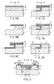
- the fifth embodiment uses, as a starting material, a bulk strained Si substrate 2 prepared by forming a strained Si layer 14 on, e.g., a 2 ⁇ m thick relaxed SiGe layer 12 on an Si substrate 1.
- a semiconductor substrate according to the fifth embodiment has a strained Si region A3 including a strained Si layer 21 on the relaxed SiGe layer 12, and a relaxed Si region B1 including a relaxed Si layer 22 without stress on a selective epitaxial Si layer 15, by epitaxially growing Si on the entire surface, as shown in FIG. 13. That is, this semiconductor substrate has the strained Si region A3 and relaxed Si region B1 at almost the same level.
- the film thickness of the strained Si layer 21 can be easily controlled, and a high-quality strained Si region A3 and relaxed Si region B1 can be formed.
- the strained state of the surface of the semiconductor substrate manufactured according to the fifth embodiment was evaluated by Raman spectroscopy analysis. It was confirmed that the strained Si layer 21 was formed on the relaxed SiGe layer 12 and the relaxed Si layer 22 without stress was formed on the epitaxial Si layer 15.
- an nMOS having, a source/drain SDa, gate insulator GIa, and gate electrode GEa is formed in the relaxed Si region B1.
- a trench DRAM cell having a source/drain SDb, gate insulator GIb, gate electrode GEb, and trench capacitor TC is formed in the relaxed Si region B1.
- the SiO 2 film 17 and SiN film 19 partially remain below the isolation IS at the interface between the strained Si region A3 and the relaxed Si region B1.
- the SiO 2 film 17 and SiN film 19 have an effect of completely isolating elements.
- the operation of the semiconductor device was evaluated to confirm that the operation speed was higher and the leakage current of the memory cell was lower than those of a semiconductor device manufactured by a conventional technique.
- a semiconductor substrate can be manufactured in which both the strained Si region A3 having the strained Si layer 21 on the surface and the relaxed Si region B1 having the relaxed Si layer 22 without stress are formed at almost the same level.
- a higher-speed, higher-performance semiconductor device than a semiconductor device manufactured by a conventional method can be manufactured.
- the first modification a number of manufacturing steps in the fifth embodiment is reduced and so modified as to be suited to high integration.
- the first modification employs, as a starting material, a relaxed SiGe substrate 5 prepared by forming, e.g., a 2 ⁇ m thick relaxed SiGe layer 12 on an Si substrate 1. This can omit a step of removing a strained Si layer by, e.g., thermal oxidation.
- the first modification can prevent to concentrate Ge in the surface of the relaxed SiGe layer 12 due to unexpected thermal oxidation of the relaxed SiGe layer 12 during the removal step of the strained Si layer.
- the relaxed SiGe layer 12 in the region A3, where strained Si is to be formed, is removed by anisotropic etching. Therefore, this modification can also prevent undercut below the mask SiN film 18 and SiO 2 film 16 by lateral etching, and is suitable for high integration.
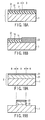
- steps (3) to (6) in the fifth embodiment are executed. More specifically, a second SiO 2 film 17 and second SiN film 19 are formed on the entire surface. The second SiN film 19 and second SiO 2 film 17 on the Si substrate 1 are removed, and an Si layer 15 is formed on the exposed Si substrate 1 by selective epitaxial growth. The SiN films 18 and 19 and the SiO 2 films 16 and 17 on the surface of the relaxed SiGe layer 12 are removed, and an Si layer is epitaxially grown on the entire surface to form Si layers 21 and 22. Consequently, as shown in FIG. 16C, a semiconductor substrate can be formed in which the strained Si layer 21 and the relaxed Si layer 22 without stress can be formed at almost the same level on the relaxed SiGe layer 12 and the epitaxial Si layer 15, respectively. In the semiconductor substrate of the first modification, the width of the boundary region between the strained Si layer 21 and the relaxed Si layer 22 without stress can be narrowed as compared with the semiconductor substrate of the fifth embodiment.
- the strained state of the surface of the semiconductor substrate manufactured according to the first modification was evaluated by Raman spectroscopy analysis. It was confirmed that the strained Si layer 21 was formed on the relaxed SiGe layer 12 and the relaxed Si layer 22 without stress was formed on the epitaxial Si layer 15.
- an nMOS is formed in the strained Si region A3, and a trench DRAM cell is formed in the relaxed Si region B1.
- the operation of the semiconductor device was evaluated to confirm that the operation speed was higher and the leakage current of the memory cell was lower than those of a semiconductor device manufactured by a conventional technique.
- a semiconductor substrate can be manufactured in which both the strained Si region A3 having the strained Si layer 21 on the surface and the relaxed Si region B1 having the relaxed Si layer 22 without stress are formed at almost the same level.
- the second modification avoids the possibility of damaging the Si substrate 1 by RIE in the forming process of the relaxed Si region B1 in the first modification.
- the second modification uses, as a starting material, a relaxed SiGe substrate 5 prepared by forming, e.g., a 2 ⁇ m thick relaxed SiGe layer 12 on an Si substrate 1.
- the second modification can simplify the process, similar to the first modification to the fifth embodiment.
- the relaxed SiGe layer 12 in the region A3 where strained Si is to be formed is removed by anisotropic etching, then, the Si substrate 1 is removed by wet etching. Undercut below the mask SiN film 18 and SiO 2 film 16 by lateral etching can be suppressed, and any damage to the Si substrate 1 by RIE can also be prevented.
- steps (3) to (6) in the fifth embodiment are executed. More specifically, a second SiO 2 film 17 and second SiN film 19 are formed on the entire surface. The second SiN film 19 and second SiO 2 film 17 on the Si substrate 1 are removed, and an Si layer 15 is formed on the exposed Si substrate 1 by selective epitaxial growth. The SiN films 18 and 19 and the SiO 2 film 16 on the surface of the relaxed SiGe layer 12 are removed, and an Si layer is epitaxially grown on the entire surface to form Si layers 21 and 22. As shown in FIG. 17C, a semiconductor substrate can be manufactured in which the strained Si layer 21 and the relaxed Si layer 22 without stress can be formed at almost the same level on the relaxed SiGe layer 12 and the epitaxial Si layer 15, respectively.
- the width of the boundary region between the strained Si layer 21 and the relaxed Si layer 22 without stress can be narrowed.
- the second modification avoids the possibility of damaging the surface of the Si substrate 1 by RIE.
- the crystallinity of the epitaxial Si layer 15 can improve.
- the strained state of the surface of the semiconductor substrate manufactured according to the second modification was evaluated by Raman spectroscopy analysis. It was confirmed that the strained Si layer 21 was formed on the relaxed SiGe layer 12 and the relaxed Si layer 22 without stress was formed on the epitaxial Si layer 15.
- an nMOS is formed in the strained Si region A3, and a trench DRAM cell is formed in the relaxed Si region B1.
- the operation of the semiconductor device was evaluated to confirm that the operation speed was higher and the leakage current of the memory cell was lower than those of a semiconductor device manufactured by a conventional technique.
- a semiconductor substrate can, therefore, be manufactured in which both the strained Si region A3 having the strained Si layer 21 on the surface and the relaxed Si region B1 having the relaxed Si layer 22 without stress are formed at almost the same level with the strained Si layer 21.
- this semiconductor substrate a higher-speed, higher-performance semiconductor device than a semiconductor device manufactured by a conventional method can be manufactured.
Landscapes
- Insulated Gate Type Field-Effect Transistor (AREA)
- Recrystallisation Techniques (AREA)
- Metal-Oxide And Bipolar Metal-Oxide Semiconductor Integrated Circuits (AREA)
- Semiconductor Memories (AREA)
- Thin Film Transistor (AREA)
- Element Separation (AREA)
Abstract
Description
Claims (19)
- A semiconductor substrate characterized by comprising:a support substrate (1);a first semiconductor region (B1, B2, B3) including a first silicon layer (22) formed above the support substrate (1);a second semiconductor region (A1, A2, A3) including a strained second silicon layer (21), a surface of the second silicon layer (21) being formed at substantially the same level as a surface of the first silicon layer (22) above the support substrate (1); andan insulating film (17, 18, 19) on an interface between the first semiconductor region (B1, B2, B3) and the second semiconductor region (A1, A2, A3).
- The substrate according to claim 1, characterized in thatthe first semiconductor region (B1) includes a first silicon layer (22) which is formed on a third silicon layer (15) above the support substrate (1); andthe second semiconductor region (A3) includes a strained second silicon layer (21) which is formed on a silicon germanium layer (12) above the support substrate (1).
- The substrate according to claim 1, characterized in thatthe first semiconductor region (B1) includes a first silicon layer (22) which is formed on a third silicon layer (15) above the support substrate (1); andthe second semiconductor region (A1) includes a strained second silicon layer (21) which is formed on a silicon germanium layer (12) over an insulating layer (11) above the support substrate (1).
- The substrate according to claim 1, characterized in thatthe first semiconductor region (B2) includes a first silicon layer (22) which is formed on a first silicon germanium layer (13) over a third silicon layer (15) above the support substrate (1); andthe second semiconductor region (A1) includes a strained second silicon layer (21) which is formed on a second silicon germanium layer (12) over an insulating layer (11) above the support substrate (1).
- The substrate according to claim 1, characterized in that the second semiconductor region (A2) includes a strained second silicon layer (21) which is formed on a silicon germanium layer (12) having a cavity (33) above the support substrate (1).
- The substrate according to claim 1, characterized in thatthe first semiconductor region (B2) includes a first silicon layer (22) which is formed on a first silicon germanium layer (13) over a third silicon layer (15) above the support substrate (1), andthe second semiconductor region (A3) includes a strained second silicon layer (21) which is formed on a second silicon germanium layer (12-1, 12-2) above the support substrate (1).
- The substrate according to any one of claims 1 to 6, characterized in that the first silicon layer (22) includes an silicon layer without stress.
- A semiconductor device characterized by comprising:a support substrate (1);a first semiconductor region (B1) including a second silicon layer (22) formed on a first silicon layer (15) above the support substrate (1);a second semiconductor region (A1, A3) including a strained third silicon layer (21) formed on a silicon germanium layer (12) above the support substrate (1), a surface of the third silicon layer (21) being formed at substantially the same level as a surface of the second silicon layer (22);an insulating film (17, 18, 19) which is formed on an interface between the first semiconductor region (B1) and the second semiconductor region (A1, A3) below an isolation insulator (IS) formed between the first semiconductor region (B1) and the second semiconductor region (A1, A3) ;a trench memory cell which is formed in the first semiconductor region (B1); anda field effect transistor which is formed in the second semiconductor region (A1, A3).
- The device according to claim 8, characterized in thatthe second semiconductor region (A1) includes a strained third silicon layer (21) which is formed on a silicon germanium layer (12) over an insulating layer (11) above the support substrate (1), a surface of the third silicon layer (21) being formed at substantially the same level as the surface of the second silicon layer (22).
- A semiconductor device characterized by comprising:a support substrate (1);a first semiconductor region (B2) including a second silicon layer (22) formed on a first silicon germanium layer (13) over a first silicon layer (15) above the support substrate (1);a second semiconductor region (A1) including a third strained silicon layer (21) formed on a second silicon germanium layer (12) over an insulating layer (11) above the support substrate (1), a surface of the third silicon layer (21) being formed at substantially the same level as a surface of the second silicon layer (22);an insulating film (17, 18) which is formed on an interface between the first semiconductor region (B2) and the second semiconductor region (A1) below an isolation insulator (IS) formed between the first semiconductor region (B2) and the second semiconductor region (A1);a first field effect transistor which is formed in the first semiconductor region (B2); anda second field effect transistor which is formed in the second semiconductor region (A1) and has a conductivity type opposite to a conductivity type of the first field effect transistor.
- A semiconductor substrate manufacturing method characterized by comprising:forming a first insulating film (16) on a semiconductor substrate (4) including a first semiconductor layer (12);patterning the first insulating film (16);removing part of the semiconductor substrate (4) to form a recess;forming a second insulating film (17, 18) on an entire surface;removing the second insulating film (17, 18) from a bottom surface in the recess;forming a second semiconductor layer (15) in the recess from a material different from a material of the first semiconductor layer (12);removing the first and second insulating films (16, 17, 18) from a surface of the first semiconductor layer (12); andsimultaneously forming a first silicon layer (21) on the first semiconductor layer (12) and a second silicon layer (22) on the second semiconductor layer (15), a surface of the second silicon layer (22) being substantially flush with a surface of the first silicon layer (21).
- The method according to claim 11, characterized in thatthe first semiconductor layer (12) includes a silicon germanium layer, andthe second semiconductor layer (15) includes a silicon layer.
- The method according to claim 11 or 12, characterized in that the semiconductor substrate (4) includes a silicon germanium layer (12) which is formed on an insulating layer (11) above the support substrate (1).
- The method according to claim 13, characterized in that the recess is formed by removing the silicon germanium layer (12) and the insulating layer (11).
- The method according to claim 13 or 14, characterized in that the second silicon layer (22) is formed on a second silicon germanium layer (13) above the second semiconductor layer (15).
- The method according to any one of claims 11 to 15, characterized in thatthe first silicon layer (21) includes a strained silicon layer, andthe second silicon layer (22) includes a silicon layer without stress.
- A semiconductor substrate manufacturing method characterized by comprising:removing a first silicon layer from a substrate having the first silicon layer formed on a silicon germanium layer (12) on a support substrate (1);forming a first insulating film (16, 18) on an entire surface;patterning the first insulating film (16, 18);removing the silicon germanium layer (12) and a part of the support substrate (1);forming a second insulating film (17, 19) on the support substrate (1) and a side surface of the silicon germanium layer (12);removing the second insulating film (17, 19) on the support substrate (1);forming a second silicon layer (15) on the support substrate (1);removing the first and second insulating films (16, 17, 18, 19) from a surface of the silicon germanium layer (12); andsimultaneously forming a third silicon layer (22) on the second silicon layer (15) and a fourth silicon layer (21) on the silicon germanium layer (12), a surface of the fourth silicon layer (21) being substantially flush with a surface of the third silicon layer (22).
- A semiconductor substrate manufacturing method characterized by comprising:forming a first insulating film (16) on a support substrate (1);patterning the first insulating film (16);removing part of the support substrate (1) to form a recess;forming a second insulating film (17, 18) on an entire surface;removing the second insulating film (17, 18) on a bottom surface of the recess in the support substrate (1);forming a silicon germanium layer (13) in the recess in the support substrate (1);forming a trench (32) in the silicon germanium layer (13);annealing the support substrate (1) in hydrogen to change the silicon germanium layer (13) into a relaxed silicon germanium layer (12) and form a cavity (33) in the relaxed silicon germanium layer (12);removing the first insulating film (16) from a surface of the support substrate (1); andsimultaneously forming a first silicon layer (22) on the support substrate (1) and a second silicon layer (21) on the silicon germanium layer (12), a surface of the second silicon layer (21) being is substantially flush with a surface of the first silicon layer (22).
- A semiconductor substrate manufacturing method characterized by comprising:forming a first insulating film (16) on a support substrate (1);patterning the first insulating film (16);forming a first silicon germanium layer (12-1, 35) on an entire surface;removing the first silicon germanium layer (35) on the first insulating film (16) to form a recess;forming a second insulating film (17, 18) on an entire surface;removing the second insulating film (17, 18) on a bottom surface of the recess;forming a first silicon layer (15) on the support substrate (1);removing the second insulating film (17, 18) from a surface of the first silicon germanium layer (12-1);forming a second silicon germanium layer (13) on the first silicon layer (15) and a third silicon germanium layer (12-2) on the first silicon germanium layer (12-1) at the same time as the second silicon germanium layer (13); andsimultaneously forming a second silicon layer (22) on the second silicon germanium layer (13) and a third silicon layer (21) on the third silicon germanium layer (12-2), a surface of the third silicon layer (21) being substantially flush with a surface of the second silicon layer (22).
Applications Claiming Priority (2)
| Application Number | Priority Date | Filing Date | Title |
|---|---|---|---|
| JP2004074969A JP4177775B2 (en) | 2004-03-16 | 2004-03-16 | Semiconductor substrate, manufacturing method thereof, and semiconductor device |
| JP2004074969 | 2004-03-16 |
Publications (2)
| Publication Number | Publication Date |
|---|---|
| EP1577943A2 true EP1577943A2 (en) | 2005-09-21 |
| EP1577943A3 EP1577943A3 (en) | 2007-08-01 |
Family
ID=34836517
Family Applications (1)
| Application Number | Title | Priority Date | Filing Date |
|---|---|---|---|
| EP04011379A Withdrawn EP1577943A3 (en) | 2004-03-16 | 2004-05-13 | Semiconductor substrate, manufacturing method therefor, and semiconductor device |
Country Status (4)
| Country | Link |
|---|---|
| US (1) | US7525154B2 (en) |
| EP (1) | EP1577943A3 (en) |
| JP (1) | JP4177775B2 (en) |
| CN (1) | CN1314120C (en) |
Cited By (1)
| Publication number | Priority date | Publication date | Assignee | Title |
|---|---|---|---|---|
| DE102009014507B4 (en) * | 2009-03-24 | 2017-08-31 | Texas Instruments Deutschland Gmbh | A method of forming an electrical contact between a carrier wafer and the surface of an upper silicon layer of a silicon-on-insulator wafer and electrical device having such an electrical contact |
Families Citing this family (21)
| Publication number | Priority date | Publication date | Assignee | Title |
|---|---|---|---|---|
| WO2003017336A2 (en) * | 2001-08-13 | 2003-02-27 | Amberwave Systems Corporation | Dram trench capacitor and method of making the same |
| JP4177775B2 (en) * | 2004-03-16 | 2008-11-05 | 株式会社東芝 | Semiconductor substrate, manufacturing method thereof, and semiconductor device |
| US7172930B2 (en) * | 2004-07-02 | 2007-02-06 | International Business Machines Corporation | Strained silicon-on-insulator by anodization of a buried p+ silicon germanium layer |
| US7384829B2 (en) | 2004-07-23 | 2008-06-10 | International Business Machines Corporation | Patterned strained semiconductor substrate and device |
| US7348635B2 (en) * | 2004-12-10 | 2008-03-25 | International Business Machines Corporation | Device having enhanced stress state and related methods |
| US7037856B1 (en) * | 2005-06-10 | 2006-05-02 | Sharp Laboratories Of America, Inc. | Method of fabricating a low-defect strained epitaxial germanium film on silicon |
| JP2007103842A (en) * | 2005-10-07 | 2007-04-19 | Toshiba Corp | Semiconductor device |
| JP2007329200A (en) * | 2006-06-06 | 2007-12-20 | Toshiba Corp | Manufacturing method of semiconductor device |
| JP5160080B2 (en) * | 2006-06-23 | 2013-03-13 | アイメック | Method for manufacturing strained multi-gate transistor and device obtained therefrom |
| US7510929B2 (en) * | 2006-10-18 | 2009-03-31 | Macronix International Co., Ltd. | Method for making memory cell device |
| US7718496B2 (en) * | 2007-10-30 | 2010-05-18 | International Business Machines Corporation | Techniques for enabling multiple Vt devices using high-K metal gate stacks |
| US20100102393A1 (en) * | 2008-10-29 | 2010-04-29 | Chartered Semiconductor Manufacturing, Ltd. | Metal gate transistors |
| CN102054735A (en) * | 2009-10-28 | 2011-05-11 | 上海华虹Nec电子有限公司 | Method for filling high-aspect ratio groove isolation area |
| CN102446853A (en) * | 2010-09-30 | 2012-05-09 | 中国科学院微电子研究所 | Strained semiconductor channel forming method and semiconductor device |
| US8680576B2 (en) * | 2012-05-16 | 2014-03-25 | Taiwan Semiconductor Manufacturing Company, Ltd. | CMOS device and method of forming the same |
| KR102210325B1 (en) * | 2013-09-06 | 2021-02-01 | 삼성전자주식회사 | Complementary metal oxide semiconductor device and method of manufacturing the same |
| US9209065B1 (en) | 2014-09-11 | 2015-12-08 | International Business Machines Corporation | Engineered substrate and device for co-integration of strained silicon and relaxed silicon |
| US9472575B2 (en) | 2015-02-06 | 2016-10-18 | International Business Machines Corporation | Formation of strained fins in a finFET device |
| US9496185B2 (en) | 2015-03-27 | 2016-11-15 | International Business Machines Corporation | Dual channel finFET with relaxed pFET region |
| US9972622B2 (en) | 2015-05-13 | 2018-05-15 | Imec Vzw | Method for manufacturing a CMOS device and associated device |
| CN109637974A (en) * | 2018-12-19 | 2019-04-16 | 上海华力集成电路制造有限公司 | A kind of FDSOI formation method |
Family Cites Families (31)
| Publication number | Priority date | Publication date | Assignee | Title |
|---|---|---|---|---|
| US5155571A (en) * | 1990-08-06 | 1992-10-13 | The Regents Of The University Of California | Complementary field effect transistors having strained superlattice structure |
| JP3372158B2 (en) | 1996-02-09 | 2003-01-27 | 株式会社東芝 | Semiconductor device and manufacturing method thereof |
| US5847419A (en) * | 1996-09-17 | 1998-12-08 | Kabushiki Kaisha Toshiba | Si-SiGe semiconductor device and method of fabricating the same |
| US6399970B2 (en) * | 1996-09-17 | 2002-06-04 | Matsushita Electric Industrial Co., Ltd. | FET having a Si/SiGeC heterojunction channel |
| EP0838858B1 (en) * | 1996-09-27 | 2002-05-15 | Infineon Technologies AG | CMOS integrated circuit and method of manufacturing the same |
| JP4258034B2 (en) * | 1998-05-27 | 2009-04-30 | ソニー株式会社 | Semiconductor device and manufacturing method of semiconductor device |
| DE10025264A1 (en) * | 2000-05-22 | 2001-11-29 | Max Planck Gesellschaft | Field effect transistor based on embedded cluster structures and method for its production |
| JP3998408B2 (en) * | 2000-09-29 | 2007-10-24 | 株式会社東芝 | Semiconductor device and manufacturing method thereof |
| JP3678661B2 (en) * | 2001-03-08 | 2005-08-03 | シャープ株式会社 | Semiconductor device |
| US20020167048A1 (en) * | 2001-05-14 | 2002-11-14 | Tweet Douglas J. | Enhanced mobility NMOS and PMOS transistors using strained Si/SiGe layers on silicon-on-insulator substrates |
| WO2003017336A2 (en) * | 2001-08-13 | 2003-02-27 | Amberwave Systems Corporation | Dram trench capacitor and method of making the same |
| JP3984014B2 (en) * | 2001-09-26 | 2007-09-26 | 株式会社東芝 | Method for manufacturing substrate for semiconductor device and substrate for semiconductor device |
| JP4322453B2 (en) * | 2001-09-27 | 2009-09-02 | 株式会社東芝 | Semiconductor device and manufacturing method thereof |
| JP3943932B2 (en) * | 2001-12-27 | 2007-07-11 | 株式会社東芝 | Manufacturing method of semiconductor device |
| US6569729B1 (en) * | 2002-07-19 | 2003-05-27 | Taiwan Semiconductor Manufacturing Company | Method of fabricating three dimensional CMOSFET devices for an embedded DRAM application |
| US6635909B2 (en) * | 2002-03-19 | 2003-10-21 | International Business Machines Corporation | Strained fin FETs structure and method |
| DE10218381A1 (en) * | 2002-04-24 | 2004-02-26 | Forschungszentrum Jülich GmbH | Method for producing one or more single-crystalline layers, each with a different lattice structure, in one plane of a layer sequence |
| JP3506694B1 (en) * | 2002-09-02 | 2004-03-15 | 沖電気工業株式会社 | MOSFET device and manufacturing method thereof |
| JP2004165197A (en) | 2002-11-08 | 2004-06-10 | Renesas Technology Corp | Semiconductor integrated circuit device and method of manufacturing the same |
| US7262451B2 (en) * | 2003-01-08 | 2007-08-28 | International Business Machines Corporation | High performance embedded DRAM technology with strained silicon |
| US6963078B2 (en) * | 2003-03-15 | 2005-11-08 | International Business Machines Corporation | Dual strain-state SiGe layers for microelectronics |
| US6927414B2 (en) * | 2003-06-17 | 2005-08-09 | International Business Machines Corporation | High speed lateral heterojunction MISFETs realized by 2-dimensional bandgap engineering and methods thereof |
| US6943407B2 (en) * | 2003-06-17 | 2005-09-13 | International Business Machines Corporation | Low leakage heterojunction vertical transistors and high performance devices thereof |
| JP2005072084A (en) * | 2003-08-28 | 2005-03-17 | Toshiba Corp | Semiconductor device and manufacturing method thereof |
| US7034362B2 (en) * | 2003-10-17 | 2006-04-25 | International Business Machines Corporation | Double silicon-on-insulator (SOI) metal oxide semiconductor field effect transistor (MOSFET) structures |
| US7247534B2 (en) * | 2003-11-19 | 2007-07-24 | International Business Machines Corporation | Silicon device on Si:C-OI and SGOI and method of manufacture |
| US7183593B2 (en) * | 2003-12-05 | 2007-02-27 | Taiwan Semiconductor Manufacturing Company, Ltd. | Heterostructure resistor and method of forming the same |
| DE10360774A1 (en) | 2003-12-23 | 2005-07-28 | Robert Bosch Gmbh | Method of manufacturing a fuel injector and fuel injector |
| JP2005244020A (en) * | 2004-02-27 | 2005-09-08 | Toshiba Corp | Semiconductor device and manufacturing method thereof |
| US7923782B2 (en) * | 2004-02-27 | 2011-04-12 | International Business Machines Corporation | Hybrid SOI/bulk semiconductor transistors |
| JP4177775B2 (en) * | 2004-03-16 | 2008-11-05 | 株式会社東芝 | Semiconductor substrate, manufacturing method thereof, and semiconductor device |
-
2004
- 2004-03-16 JP JP2004074969A patent/JP4177775B2/en not_active Expired - Fee Related
- 2004-05-13 EP EP04011379A patent/EP1577943A3/en not_active Withdrawn
- 2004-05-25 US US10/852,511 patent/US7525154B2/en not_active Expired - Fee Related
-
2005
- 2005-03-15 CN CNB2005100553053A patent/CN1314120C/en not_active Expired - Fee Related
Cited By (1)
| Publication number | Priority date | Publication date | Assignee | Title |
|---|---|---|---|---|
| DE102009014507B4 (en) * | 2009-03-24 | 2017-08-31 | Texas Instruments Deutschland Gmbh | A method of forming an electrical contact between a carrier wafer and the surface of an upper silicon layer of a silicon-on-insulator wafer and electrical device having such an electrical contact |
Also Published As
| Publication number | Publication date |
|---|---|
| CN1314120C (en) | 2007-05-02 |
| EP1577943A3 (en) | 2007-08-01 |
| CN1670956A (en) | 2005-09-21 |
| JP2005268322A (en) | 2005-09-29 |
| JP4177775B2 (en) | 2008-11-05 |
| US20050205929A1 (en) | 2005-09-22 |
| US7525154B2 (en) | 2009-04-28 |
Similar Documents
| Publication | Publication Date | Title |
|---|---|---|
| US7525154B2 (en) | Semiconductor substrate, manufacturing method therefor, and semiconductor device | |
| US9653552B2 (en) | Body-tied, strained-channel multi-gate device and methods | |
| US7902008B2 (en) | Methods for fabricating a stressed MOS device | |
| US7575968B2 (en) | Inverse slope isolation and dual surface orientation integration | |
| CN100362618C (en) | A kind of semiconductor device and manufacturing method | |
| CN100356525C (en) | Strained finFETs and method of manufacture | |
| US7560328B2 (en) | Strained Si on multiple materials for bulk or SOI substrates | |
| US7670934B1 (en) | Methods for fabricating MOS devices having epitaxially grown stress-inducing source and drain regions | |
| US20080083948A1 (en) | SiGe selective growth without a hard mask | |
| JPH11340337A (en) | Semiconductor device and method of manufacturing semiconductor device | |
| US7749829B2 (en) | Step height reduction between SOI and EPI for DSO and BOS integration | |
| US7326601B2 (en) | Methods for fabrication of a stressed MOS device | |
| JP2004039831A (en) | Method for manufacturing semiconductor device | |
| US7238588B2 (en) | Silicon buffered shallow trench isolation | |
| US8895381B1 (en) | Method of co-integration of strained-Si and relaxed Si or strained SiGe FETs on insulator with planar and non-planar architectures | |
| US9865511B2 (en) | Formation of strained fins in a finFET device | |
| US7378306B2 (en) | Selective silicon deposition for planarized dual surface orientation integration | |
| JPWO2005122272A1 (en) | MIS field effect transistor with strained silicon channel layer | |
| US8674444B2 (en) | Structure and method of forming a transistor with asymmetric channel and source/drain regions | |
| JP2011009580A (en) | Method of manufacturing semiconductor device |
Legal Events
| Date | Code | Title | Description |
|---|---|---|---|
| PUAI | Public reference made under article 153(3) epc to a published international application that has entered the european phase |
Free format text: ORIGINAL CODE: 0009012 |
|
| 17P | Request for examination filed |
Effective date: 20040513 |
|
| AK | Designated contracting states |
Kind code of ref document: A2 Designated state(s): AT BE BG CH CY CZ DE DK EE ES FI FR GB GR HU IE IT LI LU MC NL PL PT RO SE SI SK TR |
|
| AX | Request for extension of the european patent |
Extension state: AL HR LT LV MK |
|
| PUAL | Search report despatched |
Free format text: ORIGINAL CODE: 0009013 |
|
| AK | Designated contracting states |
Kind code of ref document: A3 Designated state(s): AT BE BG CH CY CZ DE DK EE ES FI FR GB GR HU IE IT LI LU MC NL PL PT RO SE SI SK TR |
|
| AX | Request for extension of the european patent |
Extension state: AL HR LT LV MK |
|
| 17Q | First examination report despatched |
Effective date: 20071107 |
|
| AKX | Designation fees paid |
Designated state(s): DE FR GB |
|
| STAA | Information on the status of an ep patent application or granted ep patent |
Free format text: STATUS: THE APPLICATION IS DEEMED TO BE WITHDRAWN |
|
| 18D | Application deemed to be withdrawn |
Effective date: 20080318 |