EP1577685B1 - Arrayed waveguide grating type optical multilexer/demultiplexer circuit - Google Patents
Arrayed waveguide grating type optical multilexer/demultiplexer circuit Download PDFInfo
- Publication number
- EP1577685B1 EP1577685B1 EP03768372A EP03768372A EP1577685B1 EP 1577685 B1 EP1577685 B1 EP 1577685B1 EP 03768372 A EP03768372 A EP 03768372A EP 03768372 A EP03768372 A EP 03768372A EP 1577685 B1 EP1577685 B1 EP 1577685B1
- Authority
- EP
- European Patent Office
- Prior art keywords
- waveguide
- optical
- parabola
- arrayed
- grating type
- Prior art date
- Legal status (The legal status is an assumption and is not a legal conclusion. Google has not performed a legal analysis and makes no representation as to the accuracy of the status listed.)
- Expired - Fee Related
Links
Images


Classifications
-
- G—PHYSICS
- G02—OPTICS
- G02B—OPTICAL ELEMENTS, SYSTEMS OR APPARATUS
- G02B6/00—Light guides; Structural details of arrangements comprising light guides and other optical elements, e.g. couplings
- G02B6/10—Light guides; Structural details of arrangements comprising light guides and other optical elements, e.g. couplings of the optical waveguide type
- G02B6/12—Light guides; Structural details of arrangements comprising light guides and other optical elements, e.g. couplings of the optical waveguide type of the integrated circuit kind
- G02B6/12007—Light guides; Structural details of arrangements comprising light guides and other optical elements, e.g. couplings of the optical waveguide type of the integrated circuit kind forming wavelength selective elements, e.g. multiplexer, demultiplexer
- G02B6/12009—Light guides; Structural details of arrangements comprising light guides and other optical elements, e.g. couplings of the optical waveguide type of the integrated circuit kind forming wavelength selective elements, e.g. multiplexer, demultiplexer comprising arrayed waveguide grating [AWG] devices, i.e. with a phased array of waveguides
- G02B6/12016—Light guides; Structural details of arrangements comprising light guides and other optical elements, e.g. couplings of the optical waveguide type of the integrated circuit kind forming wavelength selective elements, e.g. multiplexer, demultiplexer comprising arrayed waveguide grating [AWG] devices, i.e. with a phased array of waveguides characterised by the input or output waveguides, e.g. tapered waveguide ends, coupled together pairs of output waveguides
-
- G—PHYSICS
- G02—OPTICS
- G02B—OPTICAL ELEMENTS, SYSTEMS OR APPARATUS
- G02B6/00—Light guides; Structural details of arrangements comprising light guides and other optical elements, e.g. couplings
- G02B6/10—Light guides; Structural details of arrangements comprising light guides and other optical elements, e.g. couplings of the optical waveguide type
- G02B6/12—Light guides; Structural details of arrangements comprising light guides and other optical elements, e.g. couplings of the optical waveguide type of the integrated circuit kind
- G02B6/12007—Light guides; Structural details of arrangements comprising light guides and other optical elements, e.g. couplings of the optical waveguide type of the integrated circuit kind forming wavelength selective elements, e.g. multiplexer, demultiplexer
- G02B6/12009—Light guides; Structural details of arrangements comprising light guides and other optical elements, e.g. couplings of the optical waveguide type of the integrated circuit kind forming wavelength selective elements, e.g. multiplexer, demultiplexer comprising arrayed waveguide grating [AWG] devices, i.e. with a phased array of waveguides
- G02B6/12011—Light guides; Structural details of arrangements comprising light guides and other optical elements, e.g. couplings of the optical waveguide type of the integrated circuit kind forming wavelength selective elements, e.g. multiplexer, demultiplexer comprising arrayed waveguide grating [AWG] devices, i.e. with a phased array of waveguides characterised by the arrayed waveguides, e.g. comprising a filled groove in the array section
-
- G—PHYSICS
- G02—OPTICS
- G02B—OPTICAL ELEMENTS, SYSTEMS OR APPARATUS
- G02B6/00—Light guides; Structural details of arrangements comprising light guides and other optical elements, e.g. couplings
- G02B6/10—Light guides; Structural details of arrangements comprising light guides and other optical elements, e.g. couplings of the optical waveguide type
- G02B6/12—Light guides; Structural details of arrangements comprising light guides and other optical elements, e.g. couplings of the optical waveguide type of the integrated circuit kind
- G02B6/122—Basic optical elements, e.g. light-guiding paths
- G02B6/1228—Tapered waveguides, e.g. integrated spot-size transformers
-
- G—PHYSICS
- G02—OPTICS
- G02B—OPTICAL ELEMENTS, SYSTEMS OR APPARATUS
- G02B6/00—Light guides; Structural details of arrangements comprising light guides and other optical elements, e.g. couplings
- G02B6/10—Light guides; Structural details of arrangements comprising light guides and other optical elements, e.g. couplings of the optical waveguide type
- G02B6/12—Light guides; Structural details of arrangements comprising light guides and other optical elements, e.g. couplings of the optical waveguide type of the integrated circuit kind
- G02B2006/12035—Materials
- G02B2006/12038—Glass (SiO2 based materials)
Definitions
- the present invention relates to an arrayed waveguide grating type optical multiplexer/demultiplexer for use in optical wavelength division multiplexing communication systems.
- an arrayed waveguide grating type optical multiplexer/demultiplexer circuit is widely used in optical wavelength multiplexing and demultiplexing circuits for multiplexing a plurality of optical signals at the transmitter side or for demultiplexing a plurality of optical signals traveling through one optical fiber into different ports at the receiver side.
- Fig. 8 is a block diagram of a conventional arrayed waveguide grating type optical multiplexer/demultiplexer circuit.
- a conventional arrayed waveguide grating type optical multiplexer/demultiplexer circuit has an input waveguide 1, a first slab waveguide 2 connected to the input waveguide 1, an arrayed waveguide 3 connected to the first slab waveguide 2 and constituted of a plurality of optical waveguides sequentially becoming longer with a predetermined waveguide length differences, a second slab waveguide 4 connected to the arrayed waveguide 3, and a plurality of output waveguides 5 connected to the second slab waveguide 4 (for an example, refertoK. Okamoto, "Fundamentals of Optical Waveguides", Academic Press, pp. 346-381, 2000 ).
- These are constituted by using an optical waveguide which is made up of a core with high refractive index formed on a flat substrate 10 and a clad around the core.
- the light led into the input waveguide 1 is spread in the first slab waveguide 2 and branched to respective optical waveguides in the arrayed waveguide 3. Moreover, the light is multiplexed by the second slab waveguide 4 again and led into the output waveguides 5.
- an optical field pattern projected to an end of the first slab waveguide 2 at the arrayed waveguide 3 side is basically replicated to an end of the second slab waveguide 4 at the arrayed waveguide 3 side.
- an optical field has an inclination which depends on the wavelength of the input light.
- the optical field changes its focusing position depending on each wavelength by the inclination at the output waveguide 5 side of the second slab waveguide 4 and as a result, it is possible to demultiplex the wavelength.
- light of different wavelength is multiplexed and emitted from the input waveguide 1.
- This arrayed waveguide grating type optical multiplexer/demultiplexer circuit is becoming an indispensable optical component in optical multiplex communication systems in that it can make a single optical fiber transmit a plurality of signals of different wavelength.
- Figs. 9A and 9B are block diagrams of a conventional pass-band-expansion arrayed waveguide grating type optical multiplexer/demultiplexer circuit.
- the conventional pass-band-expansion arrayed waveguide grating type optical multiplexer/demultiplexer circuit has a configuration in which a parabola waveguide 6 in a parabolic shape is provided between the input waveguide 1 and the first slab waveguide 2 of the conventional arrayed waveguide grating type optical multiplexer/demultiplexer circuit shown in Fig. 8 .
- a parabola waveguide 6 in a parabolic shape is provided between the input waveguide 1 and the first slab waveguide 2 of the conventional arrayed waveguide grating type optical multiplexer/demultiplexer circuit shown in Fig. 8 .
- the width W of the input optical waveguide 1 contacting with the first slab waveguide 2 is defined with respect to the propagation axis Z of the optical wave by the following equation.
- Z A W 2 - W 0 2 - Z 0
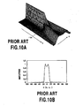
- Fig. 10A a three-dimensional distribution illustration of an optical field in the parabola waveguide 6 shown in Fig. 9B and Fig. 10B is a two-dimensional distribution illustration of an optical field in the width direction (x direction) of the parabola waveguide 6 at an end portion of the parabola waveguide 6, that is, the boundary between the parabola waveguide 6 and the first slab waveguide 2.
- the optical field in the input waveguide 1 has one peak.
- the distribution of optical fields at the boundary portion at which the parabola waveguide 6 contacts with the slab waveguide 2 has a double peak as shown in Fig. 10B . Accordingly, at the end of the second slab waveguide 4 at the output waveguide 5 side, the optical field having the double peak is also reproduced and combined with the output waveguide 5. Therefore, it is possible to expand a transmission wavelength band.
- the conventional pass-band-expansion arrayed waveguide grating type optical multiplexer/demultiplexer circuit provided with the above parabola waveguide has a serious drawback. That is, it has a high wavelength dispersion value due to a phase distribution in the parabola waveguide.
- Fig. 11 shows graphs of wavelength dispersion and loss with respect to an optical wavelength in the conventional pass-band-expansion arrayed waveguide grating type optical multiplexer/demultiplexer circuit. As obvious in Fig. 11 , it is found that the wavelength dispersion value with respect to the optical wavelength is high at the central wavelength, which is taken as a maximum wavelength dispersion value, and greatly changes in wavelength regions around the central wavelength.
- a double-peaked intensity distribution is formed at the slab interface by the parabolic waveguide horn.
- a 1dB bandwidth of 98GHz, 3dB bandwidth of 124GHz and 20dB bandwidth of 196GHz are obtained for 200GHz channel spacing.
- the crosstalk to neighbouring channels is less than -27dB and the on-chip insertion losses range from 6.1 to 6,4dB, respectively.
- document US 2002/0150338 A1 discloses an array waveguide grating module, an optical communication unit and an optical communication system. Specifically, first channel waveguides of an array waveguide grating are connected via a first to a third exponential function shape optical waveguide to a first sector-shape slab waveguide.
- second channel waveguides are connected via a first to a third taper shape optical waveguide to a second sector-shape slab waveguide.
- the present invention is made to solve the above problem and its object is to provide an arrayed waveguide grating type optical multiplexer/demultiplexer circuit with reduced wavelength dispersion.
- an arrayed waveguide grating type optical multiplexer/demultiplexer circuit of the present invention for solving the above problem is characterized in that the optical waveguide comprises a quartz-glass optical waveguide on a flat silicon substrate.
- the circuit has a parabola waveguide and the field distribution of far-fields of the parabola waveguide is equiphase and rectangular.
- the amplitude of the field distribution of far-fields of the parabola waveguide becomes a sinc function.
- Fig. 1 is an illustration showing a graph of amplitude and phase to be a sinc function.
- the variable ⁇ is an angle (rad.) value normalized by p.
- the amplitude serving as a sinc function becomes a distribution having a main peak at the center and symmetrically having a plurality of small peaks at both sides thereof.
- the field distribution of far-fields of an actual parabola waveguide becomes that of the graph shown in Fig. 2 .
- amplitudes of the field distribution of far-fields of the parabola waveguide are similar to the sinc function and show a distribution in which two side peaks (first side peaks) are present at the both sides of a main peak.
- the amplitude indicates an absolute value and the angle ⁇ is obtained by putting the traveling direction (optical axis) of a light wave incident on the parabola waveguide to 0.
- the present invention realizes an equiphase rectangular field distribution and the transmission characteristic and low-wavelength dispersion of a flat pass band by specifying the field distribution of far-fields of a parabola waveguide as an approximate scale with a sinc function in an arrayed waveguide grating type optical multiplexer/demultiplexer circuit.
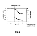
- Fig. 3 shows the relative amplitude and relative phase of a first side peak to the amplitude and phase of a main peak as an approximate scale with a sinc function in the field distribution of parabola waveguide far-fields.
- the relative amplitude and relative phase of the first side peak are calculated by Fourier-transforming the near-field pattern of a parabola waveguide obtained by using the beam propagation method.
- Fig. 3 is obtained by expressing the amplitude of the first side peak as an relative amplitude when setting the amplitude of the main peak to 1 and expressing the difference between phases of the first side peak to the phase of the main peak as the relative phase and plotting them to the variable ⁇ respectively.
- Z 0 is set to 250 ⁇ m.
- the value of Z 0 of a parabola waveguide depends on the transmission characteristic of a pass band, etc., moreover, depends on the value of A in Fig. 9B .
- the relative amplitude of a sinc function is 0.217 and the relative phase thereof is 3.14.
- Fig. 3 it is found that as the value of ⁇ increases, both of the relative amplitude and relative phase tend to decrease.
- From the viewpoint of the relative phase it is necessary to bring ⁇ to a value nearby 1.8. Therefore, though it is impossible to make the both values completely coincide with each ideal value of the sinc function, it is estimated that there is an optimum design point of the value of ⁇ between 1.5 and 1.8.
- Fig. 4 shows the wavelength dispersion characteristic in an arrayed waveguide grating type optical multiplexer/demultiplexer circuit having a parabola waveguide whose structure is specified by ⁇ and whose pass band is expanded. Moreover, this shows the dependency of wavelength dispersion on the variable ⁇ showing the structure of a parabola waveguide on a wavelength (for example, wavelength close to 1, 550 nm in Fig. 11 ) for providing highest wavelength dispersion in a channel.
- This arrayed waveguide grating type optical multiplexer/demultiplexer circuit has a channel spacing of 50 GHz.
- wavelength dispersion becomes zero.
- This value ranges between 1.5 and 1.8 and therefore, it is possible to confirm the presence of the optimum design point as previously described. That is, by properly setting the variable ⁇ showing the structure of a parabola waveguide, the field distribution of far-fields of the parabola waveguide is properly defined and this represents that a wavelength dispersion value is resultantly decreased.
- the variable ⁇ becomes an opt imum value for reducing wavelength dispersion under a condition (refer to Fig. 3 ) determined by ⁇ to take 0.217 as an upper limit in an relative amplitude and ⁇ to take 3.14 as a lower limit in a relative phase. Therefore, it is possible to simultaneously realize the broad band characteristic of a transmission wavelength of a conventional parabola waveguide and the low wavelength dispersion characteristic which has not been realized so far at the same time.
- the whole arrayed waveguide grating type optical multiplexer/demultiplexer circuit is analyzed through numerical calculation to derive wavelength dispersion from second order differentiation of the phase angle of the transfer function of the analyzed value.
- the procedure for deriving wavelength dispersion can be omitted by using the variable ⁇ , it is possible to provide a guide for properly determining the length of a parabola waveguide and greatly shorten the design time for optical circuit manufacturing.
- Fig. 5A shows a block diagram of an arrayed waveguide grating type optical multiplexer/demultiplexer circuit serving as an embodiment of the present invention for realizing the above advantage and the circuit is described in detail by referring to Fig. 5A .
- an arrayed waveguide grating type optical multiplexer/demultiplexer circuit of the present invention shown in Fig. 5A may have almost the same configuration as a conventional arrayed waveguide grating type optical multiplexer/demultiplexer circuit shown in Fig. 8 .
- the circuit has an input waveguide 1 serving as a first optical waveguide, a first slab waveguide 2 connected to the input waveguide 1, an arrayed waveguide 3 constituted of a plurality of optical waveguides which are connected to the first slab waveguide 2 and whose lengths sequentially become longer with a predetermined waveguide length difference, a second slab waveguide 4 connected to the arrayed waveguide 3, and an output waveguide 5 serving as second optical waveguides and a plurality thereof connected to the second slab waveguide 4.
- These are constituted by using a core formed on a flat substrate 10 and having a high refractive index and an optical waveguide constituted of a clad around the core. It is also allowed to use a plurality of input waveguides 1.
- a parabola waveguide 6 in a parabolic shape is arranged between the input waveguide 1 and the first slab waveguide 2.
- the parabola waveguide 6 may be the same as that shown in Fig. 9B .
- W 0 as the width of the input waveguide 1
- Z 0 as the length of the parabola waveguide 6 from the first slab waveguide 2
- the width W of the input optical waveguide 1 contacting with the first slab waveguide 2 is defined by the following equation with respect to the propagation axis Z of optical wave (refer to Fig. 5B ).
- Z A W 2 - W 0 2 - Z 0 In this case, the following conditions are satisfied: 0 ⁇ Z ⁇ -Z 0 ' and A>0.
- Z 0 is set so that the structure of the parabola waveguide defined by the above equation (1) has the variable ⁇ with low wavelength dispersion in accordance with the graphs shown in Figs. 3 and 4 . That is, it requires conditions that the parabola waveguide length Z 0 is present in a range decided by Z a,0 in which a ratio in the amplitude absolute value between the main peak and the first side peaks of the field distribution for the parabola waveguide far-fields has a value of 0.217 and Z p,0 in which a relative phase between the main peak and the first side peaks in the field distribution for the parabola waveguide far-fields has a value of 3.14 radian. That is, the condition of Z 0 is Z a , 0 ⁇ Z 0 ⁇ Z p , 0 .
- a taper waveguide 7 is further arranged between the second slab waveguide 4 and the output waveguide 5.
- W 0 ' as the width of the output waveguide 5
- Z 0 ' as the length of the taper waveguide 7 from the second slab waveguide 4
- the width W' of the output optical waveguide 5 contacting with the second slab waveguide 4 is defined by the following equation with respect to the propagation axis Z of optical wave ( Fig. 5C ).
- Z A ⁇ W ⁇ - W 0 ⁇ ⁇ - Z 0 ⁇ ⁇
- the following conditions are satisfied: 0 ⁇ Z ⁇ -Z 0 ' and A ⁇ 0.
- the above taper waveguide includes an optical waveguide with constant width when A' is equal to 0, that is, the inclination of the taper waveguide is 0. But it is not always necessary that the waveguide has a tapered shape.
- a lower clad glass soot 12 mainly containing SiO 2 and core glass soot 13 obtained by adding GeO 2 to SiO 2 are deposited on a silicon substrate 11 serving as a flat substrate by using the Flame Hydrate Deposition method ( Fig. 6A ).
- the lower clad glass soot 12 becomes a lower clad glass layer 14 and the core glass soot 13 becomes core glass 15.
- the lower clad glass soot 12 and core glass soot 13 are deposited so that the lower clad glass layer 14 has a thickness of 30 ⁇ m and the core glass 15 has a thickness of 7 ⁇ m ( Fig. 6B ).
- an etching mask 16 is formed on the core glass 15 by using the photolithography technique ( Fig. 6C ) to pattern the core glass 15 through reactive ion etching ( Fig. 6D ).
- an optical waveguide having the shape shown in Fig. 5 is formed.
- an upper clad glass 17 is formed again by the Flame Hydrate Deposition method.
- a dopant such as B 2 O 3 or P 2 O 5 is added to the upper clad glass 17 to lower a glass transition temperature and the upper clad glass 17 is filled in the narrow gap between the patterned core glasses 15 ( Fig. 6E ).
- the above optical circuit shows an arrayed waveguide grating type optical multiplexer/demultiplexer circuit in which an optical waveguide is constituted of a quartz glass optical waveguide on a flat silicon substrate as an embodiment of the present invention. Even if the material of the optical waveguide is polyimide, silicone, semiconductor, LiNbO 3 or the like, the present invention can be applied. Moreover, the flat substrate is not restricted to silicon.
- Fig. 4 the wavelength dispersion of an arrayed waveguide grating type optical multiplexer/demultiplexer circuit in which a parabola waveguide length is designed in a range of 250 to 600 pm is measured.
- a low wavelength dispersion characteristic of -15 ps/nm or less is realized and it is possible to almost flatten the wavelength dispersion to a wavelength within 3 dB band.
- This wavelength dispersion is greatly decreased up to almost 1/4 (approx. 26%) compared to the dispersion value -58 ps/nm according to conventional design shown in Fig. 4 .
- the present invention makes it possible to expand the transmission pass band of an arrayed waveguide grating type optical multiplexer/demultiplexer circuit and realize reduction of wavelength dispersion which has not been achieved so far at the same time. Moreover, by providing a parabola waveguide design guide which is not clarified in the prior art, it is possible to design efficiently.
Description
- The present invention relates to an arrayed waveguide grating type optical multiplexer/demultiplexer for use in optical wavelength division multiplexing communication systems.
- At present, development of an optical wavelength division multiplexing communication system using a plurality of optical wavelengths being actively pursued in order to increase communication capacity. In this optical wavelength division multiplexing communication system, an arrayed waveguide grating type optical multiplexer/demultiplexer circuit is widely used in optical wavelength multiplexing and demultiplexing circuits for multiplexing a plurality of optical signals at the transmitter side or for demultiplexing a plurality of optical signals traveling through one optical fiber into different ports at the receiver side.
-
Fig. 8 is a block diagram of a conventional arrayed waveguide grating type optical multiplexer/demultiplexer circuit. - As shown in
Fig. 8 , a conventional arrayed waveguide grating type optical multiplexer/demultiplexer circuit has aninput waveguide 1, afirst slab waveguide 2 connected to theinput waveguide 1, anarrayed waveguide 3 connected to thefirst slab waveguide 2 and constituted of a plurality of optical waveguides sequentially becoming longer with a predetermined waveguide length differences, asecond slab waveguide 4 connected to thearrayed waveguide 3, and a plurality ofoutput waveguides 5 connected to the second slab waveguide 4 (for an example, refertoK. Okamoto, "Fundamentals of Optical Waveguides", Academic Press, pp. 346-381, 2000). These are constituted by using an optical waveguide which is made up of a core with high refractive index formed on aflat substrate 10 and a clad around the core. - In the case of the conventional arrayed waveguide grating type optical multiplexer/demultiplexer circuit shown in
Fig. 8 , the light led into theinput waveguide 1 is spread in thefirst slab waveguide 2 and branched to respective optical waveguides in thearrayed waveguide 3. Moreover, the light is multiplexed by thesecond slab waveguide 4 again and led into theoutput waveguides 5. In this case, an optical field pattern projected to an end of thefirst slab waveguide 2 at thearrayed waveguide 3 side is basically replicated to an end of thesecond slab waveguide 4 at thearrayed waveguide 3 side. - Furthermore, because the
arrayed waveguide 3 is provided so that adjacent optical waveguides differ from each other in optical path length by ΔL, an optical field has an inclination which depends on the wavelength of the input light.
The optical field changes its focusing position depending on each wavelength by the inclination at theoutput waveguide 5 side of thesecond slab waveguide 4 and as a result, it is possible to demultiplex the wavelength. Upon receiving light from theoutput waveguide 5 side, due to reciprocity of light, light of different wavelength is multiplexed and emitted from theinput waveguide 1. - This arrayed waveguide grating type optical multiplexer/demultiplexer circuit is becoming an indispensable optical component in optical multiplex communication systems in that it can make a single optical fiber transmit a plurality of signals of different wavelength.
- Moreover, various pass-band-expansion arrayed waveguide grating type optical multiplexer/demultiplexer circuits have been proposed which respectively expand the transmission wavelength band width of the arrayed waveguide grating type optical multiplexer/demultiplexer circuit shown in
Fig. 8 (for an example, refer to K. Okamoto and A. Sugita, "Flat spectral response arrayed-Waveguide grating multiplexer with Parabola waveguide horns", Electronics Letters, Vol. 32, No. 18, pp. 1661-1662, 1996). -
Figs. 9A and 9B are block diagrams of a conventional pass-band-expansion arrayed waveguide grating type optical multiplexer/demultiplexer circuit. - As shown in
Fig. 9A , the conventional pass-band-expansion arrayed waveguide grating type optical multiplexer/demultiplexer circuit has a configuration in which aparabola waveguide 6 in a parabolic shape is provided between theinput waveguide 1 and thefirst slab waveguide 2 of the conventional arrayed waveguide grating type optical multiplexer/demultiplexer circuit shown inFig. 8 . As shown inFig. 9B , when expressing a coefficient as A, the width of theinput waveguide 1 as W0, and the length of theparabola waveguide 6 from thefirst slab waveguide 2 as Z0, the width W of the inputoptical waveguide 1 contacting with thefirst slab waveguide 2 is defined with respect to the propagation axis Z of the optical wave by the following equation.
- When using this
parabola waveguide 6, an optical field formed by theparabola waveguide 6 becomes distributions shown inFigs. 10A and 10B. Fig. 10A a three-dimensional distribution illustration of an optical field in theparabola waveguide 6 shown inFig. 9B andFig. 10B is a two-dimensional distribution illustration of an optical field in the width direction (x direction) of theparabola waveguide 6 at an end portion of theparabola waveguide 6, that is, the boundary between theparabola waveguide 6 and thefirst slab waveguide 2. - As shown in
Fig. 10A , the optical field in theinput waveguide 1 has one peak. However, in the parabola waveguide 6 (at the right portion of the position of Z=-Z0 inFig. 10A ), a distribution of optical fields having two peaks is formed. Moreover, the distribution of optical fields at the boundary portion at which the parabola waveguide 6 contacts with theslab waveguide 2 has a double peak as shown inFig. 10B . Accordingly, at the end of thesecond slab waveguide 4 at theoutput waveguide 5 side, the optical field having the double peak is also reproduced and combined with theoutput waveguide 5. Therefore, it is possible to expand a transmission wavelength band. - However, the conventional pass-band-expansion arrayed waveguide grating type optical multiplexer/demultiplexer circuit provided with the above parabola waveguide has a serious drawback. That is, it has a high wavelength dispersion value due to a phase distribution in the parabola waveguide.
Fig. 11 shows graphs of wavelength dispersion and loss with respect to an optical wavelength in the conventional pass-band-expansion arrayed waveguide grating type optical multiplexer/demultiplexer circuit. As obvious inFig. 11 , it is found that the wavelength dispersion value with respect to the optical wavelength is high at the central wavelength, which is taken as a maximum wavelength dispersion value, and greatly changes in wavelength regions around the central wavelength. This wavelength dispersion characteristic causes a problem that an optical signal (pulse) is extremely deteriorated because the dispersion provides different delay times for optical signal spectrum components in one channel.
In the Electronic Letters, IEE Stevenage, GB, vol. 32, no. 18, August 29, 1996, pages 1661-1662, ISSN: 0013-5194 the article of OKAMOTO K. et al: "Flat spectral response arrayed-waveguide grating multiplexer with parabolic waveguide horns" discloses an eight-channel flat spectral response arrayed-waveguide grating multiplexer with parabolic waveguide horns which has been fabricated on a planar lightwave circuit (PLC). Specifically, a double-peaked intensity distribution is formed at the slab interface by the parabolic waveguide horn. A 1dB bandwidth of 98GHz, 3dB bandwidth of 124GHz and 20dB bandwidth of 196GHz are obtained for 200GHz channel spacing. The crosstalk to neighbouring channels is less than -27dB and the on-chip insertion losses range from 6.1 to 6,4dB, respectively.
Furthermore, documentUS 2002/0150338 A1 discloses an array waveguide grating module, an optical communication unit and an optical communication system. Specifically, first channel waveguides of an array waveguide grating are connected via a first to a third exponential function shape optical waveguide to a first sector-shape slab waveguide. In a second boundary part which is disposed symmetrically with a first boundary part via a channel waveguide array, second channel waveguides are connected via a first to a third taper shape optical waveguide to a second sector-shape slab waveguide. By adopting exponential function shape optical waveguides at least partly, the optical frequency characteristics can be improved compared to the case of the second degree function shape, and also the degree of freedom can also be improved compared to the case of the rectangular shape. - The present invention is made to solve the above problem and its object is to provide an arrayed waveguide grating type optical multiplexer/demultiplexer circuit with reduced wavelength dispersion.
- An arrayed waveguide grating type optical multiplexer/demultiplexer circuit for solving the above problem is constituted by using optical waveguides provided with a core with high refractive index on a flat substrate and a clad around the core; and comprises a plurality of first optical waveguides, a first slab waveguide connected to the first optical waveguides, an arrayed waveguide constituted of a plurality of optical waveguides which are connected to the first slab waveguide and each of which length sequentially becomes longer with a prescribed waveguide length difference, a second slab waveguide connected to the arrayed waveguide, and a plurality of second optical waveguides connected to the second slab waveguide; further comprises
a parabola waveguide in which a width W of the first optical waveguide contacting with the first slab waveguide is defined by the following equation with respect to the propagation axis Z of optical wave:
a taper waveguide in which a width W' of the second optical waveguide contacting with the second slab waveguide is defined by the following equation with respect to the propagation axis Z of optical wave:
- Moreover, an arrayed waveguide grating type optical multiplexer/demultiplexer circuit of the present invention for solving the above problem is characterized in that the optical waveguide comprises a quartz-glass optical waveguide on a flat silicon substrate.
-
-
Fig. 1 is a graph showing amplitude and phase of a general sinc function; -
Fig. 2 is a graph showing amplitude and phase in the far-field of a parabola waveguide; -
Fig. 3 is a graph showing a relation between amplitude and phase of a first side peak to a main peak and variable showing structure of the parabola waveguide; -
Fig. 4 is a graph showing a relation between wavelength dispersion and variable ζ showing a structure of the parabola waveguide; -
Fig. 5A is a block diagram of an arrayed waveguide grating type optical multiplexer/demultiplexer circuit showing an embodiment of the present invention and an overall view thereof; -
Fig. 5B is a block diagram of an arrayed waveguide grating type optical multiplexer/demultiplexer circuit of an embodiment of the present invention, that is, a block diagram of a parabola waveguide; -
Fig. 5C is a block diagram of an arrayed waveguide grating type optical multiplexer/demultiplexer circuit showing an embodiment of the present invention, that is, a block diagram of a taper waveguide; -
Figs. 6A to 6E are illustrations showing manufacturing steps of an arrayed waveguide grating type optical multiplexer/demultiplexer circuit of the present invention; -
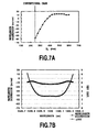
Fig. 7A is a graph showing a relation between parabola waveguide length Z0 and wavelength dispersion of an arrayed waveguide grating type optical multiplexer/demultiplexer circuit of the present invention; -
Fig. 7B is a graph showing a wavelength dispersion characteristic and loss of an arrayed waveguide grating type optical multiplexer/demultiplexer circuit of the present invention; -
Fig. 8 is a block diagram of a conventional arrayed waveguide grating type optical multiplexer/demultiplexer circuit; -
Fig. 9A is a block diagram of a conventional pass-band-expansion arrayed waveguide grating type optical multiplexer/demultiplexer circuit and an overall view of thereof; -
Fig. 9B is a block diagram of a conventional pass-band-expansion arrayed waveguide grating type optical multiplexer/demultiplexer circuit, that is, a block diagram of a parabola waveguide; -
Figs. 10A and 10B are distribution illustrations of an optical field of a parabola waveguide; and -
Fig. 11 is a graph showing a wavelength dispersion characteristic and loss of a conventional pass-band-expansion arrayed waveguide grating type optical multiplexer/demultiplexer circuit. - For an arrayed waveguide grating type optical multiplexer/demultiplexer circuit to have a pass band of a flat transmission characteristic and low wavelength dispersion, it is preferable that the circuit has a parabola waveguide and the field distribution of far-fields of the parabola waveguide is equiphase and rectangular. In this case, it is known that the amplitude of the field distribution of far-fields of the parabola waveguide becomes a sinc function.
- The equation of a general sinc function is shown below.
Fig. 1 is an illustration showing a graph of amplitude and phase to be a sinc function.
- As shown in
Fig. 1 , the amplitude serving as a sinc function becomes a distribution having a main peak at the center and symmetrically having a plurality of small peaks at both sides thereof. Moreover, the sinc function is a real function and its imaginary part is zero. Therefore, phase planes become equal. That is, a phase characteristics shows a rectangular shape having a flat phase (equiphase) portion close to the variable ξ=0. - However, the field distribution of far-fields of an actual parabola waveguide becomes that of the graph shown in
Fig. 2 . As shown inFig. 2 , amplitudes of the field distribution of far-fields of the parabola waveguide are similar to the sinc function and show a distribution in which two side peaks (first side peaks) are present at the both sides of a main peak. Moreover, phases show a distribution having an almost flat phase portion close to the angle θ=0. In the graph inFig. 2 , the amplitude indicates an absolute value and the angle θ is obtained by putting the traveling direction (optical axis) of a light wave incident on the parabola waveguide to 0. - As understood from the comparison between
Figs. 1 and2 , to realize an ideal field distribution, that is, an equiphase rectangular field distribution, it is allowed to consider the amplitude and phase of a first side peak as approximate scales with a sinc function on the basis of the amplitude and phase of the main peak in the field distribution of far-fields of an actual parabola waveguide. That is, the present invention realizes an equiphase rectangular field distribution and the transmission characteristic and low-wavelength dispersion of a flat pass band by specifying the field distribution of far-fields of a parabola waveguide as an approximate scale with a sinc function in an arrayed waveguide grating type optical multiplexer/demultiplexer circuit. -
Fig. 3 shows the relative amplitude and relative phase of a first side peak to the amplitude and phase of a main peak as an approximate scale with a sinc function in the field distribution of parabola waveguide far-fields.
Specifically, the relative amplitude and relative phase of the first side peak are calculated by Fourier-transforming the near-field pattern of a parabola waveguide obtained by using the beam propagation method.Fig. 3 is obtained by expressing the amplitude of the first side peak as an relative amplitude when setting the amplitude of the main peak to 1 and expressing the difference between phases of the first side peak to the phase of the main peak as the relative phase and plotting them to the variable ζ respectively. This variable ζ is a parameter showing the structure of a parabola waveguide and is normalized so that the length of a design value of a conventional parabola waveguide becomes ζ=1. InFig. 3 , Z0 is set to 250 µm. The value of Z0 of a parabola waveguide depends on the transmission characteristic of a pass band, etc., moreover, depends on the value of A inFig. 9B . - Referring to
Fig. 1 , the relative amplitude of a sinc function is 0.217 and the relative phase thereof is 3.14. Referring toFig. 3 , it is found that as the value of ζ increases, both of the relative amplitude and relative phase tend to decrease. To make the value of a conventional design of ζ=1 approach an ideal value of a sinc function, it is necessary to bring ζ to a value close to 1.5 from the viewpoint of the relative amplitude. Moreover, from the viewpoint of the relative phase, it is necessary to bring ζ to a value nearby 1.8. Therefore, though it is impossible to make the both values completely coincide with each ideal value of the sinc function, it is estimated that there is an optimum design point of the value of ζ between 1.5 and 1.8. - Therefore, to confirm the optimum design point of wavelength dispersion to the variable ζ,
Fig. 4 shows the wavelength dispersion characteristic in an arrayed waveguide grating type optical multiplexer/demultiplexer circuit having a parabola waveguide whose structure is specified by ζ and whose pass band is expanded. Moreover, this shows the dependency of wavelength dispersion on the variable ζ showing the structure of a parabola waveguide on a wavelength (for example, wavelength close to 1, 550 nm inFig. 11 ) for providing highest wavelength dispersion in a channel. This arrayed waveguide grating type optical multiplexer/demultiplexer circuit has a channel spacing of 50 GHz. - As shown by the graph in
Fig. 4 , when setting the variable to 1.6, wavelength dispersion becomes zero. This value ranges between 1.5 and 1.8 and therefore, it is possible to confirm the presence of the optimum design point as previously described. That is, by properly setting the variable ζ showing the structure of a parabola waveguide, the field distribution of far-fields of the parabola waveguide is properly defined and this represents that a wavelength dispersion value is resultantly decreased. Specifically, the variable ζ becomes an opt imum value for reducing wavelength dispersion under a condition (refer toFig. 3 ) determined by ζ to take 0.217 as an upper limit in an relative amplitude and ζ to take 3.14 as a lower limit in a relative phase. Therefore, it is possible to simultaneously realize the broad band characteristic of a transmission wavelength of a conventional parabola waveguide and the low wavelength dispersion characteristic which has not been realized so far at the same time. - Moreover, conventionally to derive wavelength dispersion, the whole arrayed waveguide grating type optical multiplexer/demultiplexer circuit is analyzed through numerical calculation to derive wavelength dispersion from second order differentiation of the phase angle of the transfer function of the analyzed value. However, in the present invention, because the procedure for deriving wavelength dispersion can be omitted by using the variable ζ, it is possible to provide a guide for properly determining the length of a parabola waveguide and greatly shorten the design time for optical circuit manufacturing.
-
Fig. 5A shows a block diagram of an arrayed waveguide grating type optical multiplexer/demultiplexer circuit serving as an embodiment of the present invention for realizing the above advantage and the circuit is described in detail by referring toFig. 5A . - It is allowed that an arrayed waveguide grating type optical multiplexer/demultiplexer circuit of the present invention shown in
Fig. 5A may have almost the same configuration as a conventional arrayed waveguide grating type optical multiplexer/demultiplexer circuit shown inFig. 8 . That is, the circuit has aninput waveguide 1 serving as a first optical waveguide, afirst slab waveguide 2 connected to theinput waveguide 1, an arrayedwaveguide 3 constituted of a plurality of optical waveguides which are connected to thefirst slab waveguide 2 and whose lengths sequentially become longer with a predetermined waveguide length difference, asecond slab waveguide 4 connected to the arrayedwaveguide 3, and anoutput waveguide 5 serving as second optical waveguides and a plurality thereof connected to thesecond slab waveguide 4. These are constituted by using a core formed on aflat substrate 10 and having a high refractive index and an optical waveguide constituted of a clad around the core. It is also allowed to use a plurality ofinput waveguides 1. - Moreover, a
parabola waveguide 6 in a parabolic shape is arranged between theinput waveguide 1 and thefirst slab waveguide 2. Theparabola waveguide 6 may be the same as that shown inFig. 9B . When expressing A as a coefficient, W0 as the width of theinput waveguide 1, and Z0 as the length of theparabola waveguide 6 from thefirst slab waveguide 2, the width W of the inputoptical waveguide 1 contacting with thefirst slab waveguide 2 is defined by the following equation with respect to the propagation axis Z of optical wave (refer toFig. 5B ).
- However, in the case of the present invention, Z0 is set so that the structure of the parabola waveguide defined by the above equation (1) has the variable ζ with low wavelength dispersion in accordance with the graphs shown in
Figs. 3 and4 . That is, it requires conditions that the parabola waveguide length Z0 is present in a range decided by Za,0 in which a ratio in the amplitude absolute value between the main peak and the first side peaks of the field distribution for the parabola waveguide far-fields has a value of 0.217 and Zp,0 in which a relative phase between the main peak and the first side peaks in the field distribution for the parabola waveguide far-fields has a value of 3.14 radian. That is, the condition of Z0 is Za,0≤Z0≤Zp,0. - Moreover, in the case of an arrayed waveguide grating type optical multiplexer/demultiplexer circuit of the present invention, a
taper waveguide 7 is further arranged between thesecond slab waveguide 4 and theoutput waveguide 5. In the case of thetaper waveguide 7, when expressing A' as a coefficient. W0' as the width of theoutput waveguide 5, Z0'as the length of thetaper waveguide 7 from thesecond slab waveguide 4, the width W' of the outputoptical waveguide 5 contacting with thesecond slab waveguide 4 is defined by the following equation with respect to the propagation axis Z of optical wave (Fig. 5C ).
- The above taper waveguide includes an optical waveguide with constant width when A' is equal to 0, that is, the inclination of the taper waveguide is 0. But it is not always necessary that the waveguide has a tapered shape.
- Then, a manufacturing method of a waveguide of an optical circuit of the present invention is briefly described by referring to
Figs. 6A to 6E . - A lower
clad glass soot 12 mainly containing SiO2 andcore glass soot 13 obtained by adding GeO2 to SiO2 are deposited on asilicon substrate 11 serving as a flat substrate by using the Flame Hydrate Deposition method (Fig. 6A ). - Thereafter, by transparentizing glass at a high temperature of 1,000°C or higher, the lower
clad glass soot 12 becomes a lowerclad glass layer 14 and thecore glass soot 13 becomescore glass 15. In this case, the lowerclad glass soot 12 andcore glass soot 13 are deposited so that the lowerclad glass layer 14 has a thickness of 30µm and thecore glass 15 has a thickness of 7µm (Fig. 6B ). - Then, an
etching mask 16 is formed on thecore glass 15 by using the photolithography technique (Fig. 6C ) to pattern thecore glass 15 through reactive ion etching (Fig. 6D ). In this case, an optical waveguide having the shape shown inFig. 5 is formed. - After removing the
etching mask 16, an upper cladglass 17 is formed again by the Flame Hydrate Deposition method. A dopant such as B2O3 or P2O5 is added to the upper cladglass 17 to lower a glass transition temperature and the upper cladglass 17 is filled in the narrow gap between the patterned core glasses 15 (Fig. 6E ). - The above optical circuit shows an arrayed waveguide grating type optical multiplexer/demultiplexer circuit in which an optical waveguide is constituted of a quartz glass optical waveguide on a flat silicon substrate as an embodiment of the present invention. Even if the material of the optical waveguide is polyimide, silicone, semiconductor, LiNbO3 or the like, the present invention can be applied. Moreover, the flat substrate is not restricted to silicon.
- To actually verify the dependency of the wavelength dispersion shown in
Fig. 4 on ζ, the wavelength dispersion of an arrayed waveguide grating type optical multiplexer/demultiplexer circuit in which a parabola waveguide length is designed in a range of 250 to 600 pm is measured. In this case, a parabola waveguide length Z0=250 pm according to conventional design is used as a reference.Fig. 7A shows a relation between parabola waveguide length Z0 and wavelength dispersion. That is, it is confirmed that wavelength dispersion becomes almost zero at ζ=1.6, that it Z0=400 µm -
Fig. 7B shows the wavelength dispersion characteristic and loss of an arrayed waveguide grating type optical multiplexer/demultiplexer circuit having a parabola waveguide designed by setting ζ to 1.6, that is, setting Z0 to 1.6×250=400µm and a channel spacing of 50 GHz. As shown inFig. 7B , in the case of the arrayed waveguide grating type optical multiplexer/demultiplexer circuit of the present invention, a low wavelength dispersion characteristic of -15 ps/nm or less is realized and it is possible to almost flatten the wavelength dispersion to a wavelength within 3 dB band. This wavelength dispersion is greatly decreased up to almost 1/4 (approx. 26%) compared to the dispersion value -58 ps/nm according to conventional design shown inFig. 4 . - The present invention makes it possible to expand the transmission pass band of an arrayed waveguide grating type optical multiplexer/demultiplexer circuit and realize reduction of wavelength dispersion which has not been achieved so far at the same time. Moreover, by providing a parabola waveguide design guide which is not clarified in the prior art, it is possible to design efficiently.
Claims (2)
- An arrayed waveguide grating type optical multiplexer/demultiplexer circuit, comprising on a flat substrate (10) a plurality of first optical waveguides (1), a first slab waveguide (2) which is connected to the first optical waveguides, an arrayed waveguide (3), connected to the first slab waveguide, consisting of a plurality of optical waveguides which sequentially become longer with a prescribed waveguide length difference, a second slab waveguide (4) which is connected to the arrayed waveguides, and a plurality of second optical waveguides (5) which are connected to the second slab waveguide;
a parabola waveguide (6) in which a width W of the first optical waveguide contacting with the first slab waveguide is defined by the following equation with respect to a propagation axis Z of optical wave,
where, A: a coefficient, and A>0, W0: a width of the first optical waveguide, and Z0: a length of the parabola waveguide;
and a taper waveguide (7) in which a width W' of the second optical waveguide contacting with the second slab waveguide is defined by the following equation with respect to a propagation axis Z of optical wave,
where,
A': a coefficient, W0': a width of the second optical waveguide, and Z0': a length of the taper waveguide;
characterized in that
the length Z0 is set within a range defined by the following condition,
where
Za,0: a parabola waveguide length for which a ratio of the amplitude absolute value between a main peak and first side peaks in the field distribution of the parabola waveguide far-field has a value of 0.217, and Zp,0: a parabola waveguide length for which a relative phase between the main peak and the first side peaks in the field distribution of far-field has a value of 3.14 radians. - An arrayed waveguide grating type optical multiplexer/demultiplexer circuit according to claim 1, wherein each waveguide is a silica glass optical waveguide on a flat silicon substrate.
Applications Claiming Priority (3)
| Application Number | Priority Date | Filing Date | Title |
|---|---|---|---|
| JP2002378882 | 2002-12-27 | ||
| JP2002378882A JP3775673B2 (en) | 2002-12-27 | 2002-12-27 | Arrayed waveguide grating type optical multiplexer / demultiplexer |
| PCT/JP2003/017065 WO2004061496A1 (en) | 2002-12-27 | 2003-12-26 | Array waveguide lattice type optical multilexer/demultiplexer circuit |
Publications (3)
| Publication Number | Publication Date |
|---|---|
| EP1577685A1 EP1577685A1 (en) | 2005-09-21 |
| EP1577685A4 EP1577685A4 (en) | 2006-04-12 |
| EP1577685B1 true EP1577685B1 (en) | 2010-02-17 |
Family
ID=32708354
Family Applications (1)
| Application Number | Title | Priority Date | Filing Date |
|---|---|---|---|
| EP03768372A Expired - Fee Related EP1577685B1 (en) | 2002-12-27 | 2003-12-26 | Arrayed waveguide grating type optical multilexer/demultiplexer circuit |
Country Status (8)
| Country | Link |
|---|---|
| US (1) | US7400800B2 (en) |
| EP (1) | EP1577685B1 (en) |
| JP (1) | JP3775673B2 (en) |
| KR (1) | KR100722250B1 (en) |
| CN (1) | CN100381843C (en) |
| AU (1) | AU2003292722A1 (en) |
| DE (1) | DE60331352D1 (en) |
| WO (1) | WO2004061496A1 (en) |
Families Citing this family (6)
| Publication number | Priority date | Publication date | Assignee | Title |
|---|---|---|---|---|
| JP2007286077A (en) * | 2004-05-20 | 2007-11-01 | Nec Corp | Optical multiplexer/demultiplexer |
| KR100968891B1 (en) | 2007-12-14 | 2010-07-09 | 한국전자통신연구원 | The wavelength division multiplexer/demultiplexer having flat wavelength response |
| US8086105B2 (en) | 2007-12-14 | 2011-12-27 | Electronics And Telecommunications Research Institute | Wavelength division multiplexer/demultiplexer having flat wavelength response |
| KR102364302B1 (en) | 2015-01-27 | 2022-02-21 | 한국전자통신연구원 | Flat-top mode controller and arrayed waveguide grating |
| KR102029739B1 (en) | 2015-03-27 | 2019-11-08 | 한국전자통신연구원 | Arrayed Waveguide Grating Device and Method for Manufacturing Arrayed Waveguide Grating |
| CN109597162B (en) * | 2018-12-27 | 2021-04-09 | 华为技术有限公司 | Planar optical waveguide, PLC chip, beam shaping structure and WSS |
Family Cites Families (19)
| Publication number | Priority date | Publication date | Assignee | Title |
|---|---|---|---|---|
| US5136671A (en) | 1991-08-21 | 1992-08-04 | At&T Bell Laboratories | Optical switch, multiplexer, and demultiplexer |
| JP3238266B2 (en) | 1994-01-28 | 2001-12-10 | 松下電器産業株式会社 | Switching power supply |
| JP3201560B2 (en) * | 1994-06-13 | 2001-08-20 | 日本電信電話株式会社 | Optical signal processing circuit |
| US5467418A (en) | 1994-09-02 | 1995-11-14 | At&T Ipm Corp. | Frequency routing device having a spatially filtered optical grating for providing an increased passband width |
| FR2743234B1 (en) | 1995-12-28 | 1998-01-23 | Alcatel Optronics | WAVELENGTH DEMULTIPLEXER |
| JP3112246B2 (en) * | 1996-05-01 | 2000-11-27 | 日本電信電話株式会社 | Array waveguide grating |
| JP3238890B2 (en) | 1997-11-13 | 2001-12-17 | 日本電信電話株式会社 | Array waveguide type wavelength multiplexer / demultiplexer |
| US6069990A (en) | 1997-11-27 | 2000-05-30 | Hitachi Cable Ltd. | Optical wavelength multiplexer/demultiplexer |
| US6222956B1 (en) | 1998-05-29 | 2001-04-24 | Hitachi Cable Ltd. | Optical wavelength multiplexer/demultiplexer |
| KR100293954B1 (en) | 1999-05-11 | 2001-06-15 | 윤종용 | Low loss awg demultiplexer with flat spectral response |
| JP3736303B2 (en) * | 2000-06-29 | 2006-01-18 | 日本電気株式会社 | Array waveguide grating, multiplexer device, demultiplexer device, node device, and optical communication system |
| US6298186B1 (en) * | 2000-07-07 | 2001-10-02 | Metrophotonics Inc. | Planar waveguide grating device and method having a passband with a flat-top and sharp-transitions |
| JP3735024B2 (en) | 2000-09-13 | 2006-01-11 | 住友電気工業株式会社 | Optical multiplexer / demultiplexer |
| US6633703B2 (en) * | 2000-09-13 | 2003-10-14 | Sumitomo Electric Industries, Ltd. | Optical multiplexer/demultiplexer |
| JP4659969B2 (en) * | 2000-11-15 | 2011-03-30 | 矢崎総業株式会社 | Congestion degree display system |
| JP2002311264A (en) | 2001-04-16 | 2002-10-23 | Nec Corp | Array waveguide grating, array waveguide grating module and optical communication system |
| US6563988B2 (en) * | 2001-04-25 | 2003-05-13 | Lightwave Microsystems Corporation | Optical apparatus and method having predetermined group velocity dispersion |
| US6728442B2 (en) | 2001-05-21 | 2004-04-27 | Jds Uniphase Corporation | Controlling the dispersion and passband characteristics of an arrayed waveguide grating |
| JP2003227948A (en) | 2002-02-04 | 2003-08-15 | Ntt Electornics Corp | Optical multiplexer/demultiplexer and method of manufacturing the same |
-
2002
- 2002-12-27 JP JP2002378882A patent/JP3775673B2/en not_active Expired - Lifetime
-
2003
- 2003-12-26 US US10/540,789 patent/US7400800B2/en not_active Expired - Fee Related
- 2003-12-26 AU AU2003292722A patent/AU2003292722A1/en not_active Abandoned
- 2003-12-26 EP EP03768372A patent/EP1577685B1/en not_active Expired - Fee Related
- 2003-12-26 KR KR1020057012049A patent/KR100722250B1/en not_active IP Right Cessation
- 2003-12-26 DE DE60331352T patent/DE60331352D1/en not_active Expired - Lifetime
- 2003-12-26 CN CNB200380107773XA patent/CN100381843C/en not_active Expired - Fee Related
- 2003-12-26 WO PCT/JP2003/017065 patent/WO2004061496A1/en active Application Filing
Also Published As
| Publication number | Publication date |
|---|---|
| EP1577685A1 (en) | 2005-09-21 |
| AU2003292722A1 (en) | 2004-07-29 |
| DE60331352D1 (en) | 2010-04-01 |
| KR100722250B1 (en) | 2007-05-29 |
| JP3775673B2 (en) | 2006-05-17 |
| WO2004061496A1 (en) | 2004-07-22 |
| AU2003292722A8 (en) | 2004-07-29 |
| KR20050097923A (en) | 2005-10-10 |
| JP2004212435A (en) | 2004-07-29 |
| CN1732397A (en) | 2006-02-08 |
| CN100381843C (en) | 2008-04-16 |
| US7400800B2 (en) | 2008-07-15 |
| US20060233491A1 (en) | 2006-10-19 |
| EP1577685A4 (en) | 2006-04-12 |
Similar Documents
| Publication | Publication Date | Title |
|---|---|---|
| US6757454B2 (en) | Polarization desensitized optical waveguide interferometer | |
| US6195481B1 (en) | Array waveguide diffraction grating optical multiplexer/demultiplexer | |
| JP2005010805A6 (en) | Waveguide type optical interferometer | |
| US7174071B2 (en) | Arrayed waveguide grating with increased uniformity of a performance parameter | |
| US6404946B1 (en) | Arrayed waveguide grating type optical multiplexer/demultiplexer | |
| EP1577685B1 (en) | Arrayed waveguide grating type optical multilexer/demultiplexer circuit | |
| EP1113297A2 (en) | Arrayed waveguide grating multiplexer with tapered waveguides | |
| US6798952B2 (en) | Optical multiplexer/demultiplexer | |
| US6741772B2 (en) | Optical multiplexer/demultiplexer and waveguide type optical coupler | |
| EP1111418A2 (en) | Arrayed-waveguide grating | |
| KR100446524B1 (en) | Wavelength division multiplexer / demultiplexer | |
| US6735363B1 (en) | Waveguide-grating router with output tapers configured to provide a passband that is optimized for each channel individually | |
| KR20110002619A (en) | Optical device | |
| JP3921385B2 (en) | Arrayed waveguide grating, arrayed waveguide grating module, and optical communication system | |
| CN110892302B (en) | Broadband star coupler | |
| EP1278098A2 (en) | Planar lightwave circuit type variable optical attenuator | |
| Shaari et al. | Design implementation of up to 20 channel silica-based arrayed waveguide WDM | |
| JP4163553B2 (en) | Arrayed waveguide diffraction grating type optical multiplexer / demultiplexer | |
| Takahashi | Arrayed Waveguide Grating (AWG) | |
| Fan et al. | A Flat-top Arrayed Waveguide Grating Using A MMI Based on V-shaped Subwavelength Gratings |
Legal Events
| Date | Code | Title | Description |
|---|---|---|---|
| PUAI | Public reference made under article 153(3) epc to a published international application that has entered the european phase |
Free format text: ORIGINAL CODE: 0009012 |
|
| 17P | Request for examination filed |
Effective date: 20050627 |
|
| AK | Designated contracting states |
Kind code of ref document: A1 Designated state(s): AT BE BG CH CY CZ DE DK EE ES FI FR GB GR HU IE IT LI LU MC NL PT RO SE SI SK TR |
|
| AX | Request for extension of the european patent |
Extension state: AL LT LV MK |
|
| A4 | Supplementary search report drawn up and despatched |
Effective date: 20060223 |
|
| DAX | Request for extension of the european patent (deleted) | ||
| RBV | Designated contracting states (corrected) |
Designated state(s): DE FR GB IT |
|
| GRAP | Despatch of communication of intention to grant a patent |
Free format text: ORIGINAL CODE: EPIDOSNIGR1 |
|
| GRAS | Grant fee paid |
Free format text: ORIGINAL CODE: EPIDOSNIGR3 |
|
| RAP1 | Party data changed (applicant data changed or rights of an application transferred) |
Owner name: NTT ELECTRONICS CORPORATION Owner name: NIPPON TELEGRAPH AND TELEPHONE CORPORATION |
|
| GRAA | (expected) grant |
Free format text: ORIGINAL CODE: 0009210 |
|
| AK | Designated contracting states |
Kind code of ref document: B1 Designated state(s): DE FR GB IT |
|
| REG | Reference to a national code |
Ref country code: GB Ref legal event code: FG4D |
|
| REF | Corresponds to: |
Ref document number: 60331352 Country of ref document: DE Date of ref document: 20100401 Kind code of ref document: P |
|
| PLBE | No opposition filed within time limit |
Free format text: ORIGINAL CODE: 0009261 |
|
| STAA | Information on the status of an ep patent application or granted ep patent |
Free format text: STATUS: NO OPPOSITION FILED WITHIN TIME LIMIT |
|
| 26N | No opposition filed |
Effective date: 20101118 |
|
| PGFP | Annual fee paid to national office [announced via postgrant information from national office to epo] |
Ref country code: FR Payment date: 20110107 Year of fee payment: 8 |
|
| PGFP | Annual fee paid to national office [announced via postgrant information from national office to epo] |
Ref country code: GB Payment date: 20101221 Year of fee payment: 8 |
|
| PGFP | Annual fee paid to national office [announced via postgrant information from national office to epo] |
Ref country code: DE Payment date: 20101229 Year of fee payment: 8 Ref country code: IT Payment date: 20101228 Year of fee payment: 8 |
|
| GBPC | Gb: european patent ceased through non-payment of renewal fee |
Effective date: 20111226 |
|
| REG | Reference to a national code |
Ref country code: FR Ref legal event code: ST Effective date: 20120831 |
|
| REG | Reference to a national code |
Ref country code: DE Ref legal event code: R119 Ref document number: 60331352 Country of ref document: DE Effective date: 20120703 |
|
| PG25 | Lapsed in a contracting state [announced via postgrant information from national office to epo] |
Ref country code: GB Free format text: LAPSE BECAUSE OF NON-PAYMENT OF DUE FEES Effective date: 20111226 Ref country code: DE Free format text: LAPSE BECAUSE OF NON-PAYMENT OF DUE FEES Effective date: 20120703 |
|
| PG25 | Lapsed in a contracting state [announced via postgrant information from national office to epo] |
Ref country code: IT Free format text: LAPSE BECAUSE OF NON-PAYMENT OF DUE FEES Effective date: 20111226 |
|
| PG25 | Lapsed in a contracting state [announced via postgrant information from national office to epo] |
Ref country code: FR Free format text: LAPSE BECAUSE OF NON-PAYMENT OF DUE FEES Effective date: 20120102 |