EP1577648B1 - Dispositif de mesure - Google Patents
Dispositif de mesure Download PDFInfo
- Publication number
- EP1577648B1 EP1577648B1 EP04006043A EP04006043A EP1577648B1 EP 1577648 B1 EP1577648 B1 EP 1577648B1 EP 04006043 A EP04006043 A EP 04006043A EP 04006043 A EP04006043 A EP 04006043A EP 1577648 B1 EP1577648 B1 EP 1577648B1
- Authority
- EP
- European Patent Office
- Prior art keywords
- circuit board
- sensor
- printed circuit
- module according
- teeth
- Prior art date
- Legal status (The legal status is an assumption and is not a legal conclusion. Google has not performed a legal analysis and makes no representation as to the accuracy of the status listed.)
- Expired - Lifetime
Links
- 238000007789 sealing Methods 0.000 claims description 3
- 150000001875 compounds Chemical class 0.000 claims description 2
- 238000007493 shaping process Methods 0.000 claims description 2
- 238000004519 manufacturing process Methods 0.000 abstract description 3
- WABPQHHGFIMREM-UHFFFAOYSA-N lead(0) Chemical compound [Pb] WABPQHHGFIMREM-UHFFFAOYSA-N 0.000 description 6
- 238000013461 design Methods 0.000 description 5
- 230000008901 benefit Effects 0.000 description 3
- 238000000034 method Methods 0.000 description 3
- 230000008569 process Effects 0.000 description 3
- 230000008859 change Effects 0.000 description 2
- 238000004891 communication Methods 0.000 description 2
- 238000012937 correction Methods 0.000 description 2
- 230000001419 dependent effect Effects 0.000 description 2
- 238000001514 detection method Methods 0.000 description 2
- 238000010586 diagram Methods 0.000 description 2
- 238000012544 monitoring process Methods 0.000 description 2
- 230000032683 aging Effects 0.000 description 1
- 238000004378 air conditioning Methods 0.000 description 1
- 230000005540 biological transmission Effects 0.000 description 1
- 238000005266 casting Methods 0.000 description 1
- 230000001143 conditioned effect Effects 0.000 description 1
- 238000010276 construction Methods 0.000 description 1
- 238000003745 diagnosis Methods 0.000 description 1
- 238000007599 discharging Methods 0.000 description 1
- 230000006870 function Effects 0.000 description 1
- 238000010438 heat treatment Methods 0.000 description 1
- 238000005304 joining Methods 0.000 description 1
- 230000013011 mating Effects 0.000 description 1
- 238000000465 moulding Methods 0.000 description 1
- 239000004033 plastic Substances 0.000 description 1
- 230000009467 reduction Effects 0.000 description 1
- 230000001105 regulatory effect Effects 0.000 description 1
- 239000011347 resin Substances 0.000 description 1
- 229920005989 resin Polymers 0.000 description 1
- 239000000565 sealant Substances 0.000 description 1
- 239000002356 single layer Substances 0.000 description 1
- 229910000679 solder Inorganic materials 0.000 description 1
- 238000003860 storage Methods 0.000 description 1
- 229920001169 thermoplastic Polymers 0.000 description 1
- 239000004416 thermosoftening plastic Substances 0.000 description 1
- 238000009423 ventilation Methods 0.000 description 1
Images

Classifications
-
- G—PHYSICS
- G01—MEASURING; TESTING
- G01D—MEASURING NOT SPECIALLY ADAPTED FOR A SPECIFIC VARIABLE; ARRANGEMENTS FOR MEASURING TWO OR MORE VARIABLES NOT COVERED IN A SINGLE OTHER SUBCLASS; TARIFF METERING APPARATUS; MEASURING OR TESTING NOT OTHERWISE PROVIDED FOR
- G01D11/00—Component parts of measuring arrangements not specially adapted for a specific variable
- G01D11/24—Housings ; Casings for instruments
- G01D11/245—Housings for sensors
Definitions
- the invention relates to a measuring device referred to in the preamble of claim 1 Art.
- Such measuring devices are advantageously used in heating, ventilation and air conditioning (HVAC) for buildings to capture a process variable.
- HVAC heating, ventilation and air conditioning
- Such a measuring device is an example of a device for detecting the humidity in a room or in a device for supplying or discharging air.
- Such measuring devices can also be used for detecting the illuminance or for gas detection.
- the present invention can be used in principle if process variables are detected with sensor elements having electrical connecting wires. Such a measuring device can therefore also be used in a vehicle.
- a known measuring device for detecting the humidity has a capacitive humidity sensor and a temperature sensor. For the detection of electrical measuring signals connecting wires of the two sensors are connected via plug or solder connections with an electronic circuit or with a connection cable.
- the invention is based on the object to provide a measuring device with electrical sensors in which uninsulated thin leads of a sensor - for example, those with a wire diameter in the order of 0.1 mm - reproducible, safe and inexpensive with a circuit board are connected.
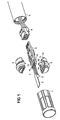
- FIG. 1, 1 designates a sensor module with a first sensor element 2 and a second sensor element 3, with a single-layer or multilayer printed circuit board 4, with a first shell 5 and a second shell 6.
- the first sensor element 2 is a humidity sensor and the second sensor element 3 is a temperature sensor.
- the two sensor elements 2 and 3 for example, the relative humidity of a room or an air duct can be detected.
- the sensor module 1 has a plurality of sensor elements or only a single sensor element.
- the two shells 5 and 6 are designed such that they put together a holding function for the sensor module 1 exercise.
- the sensor elements 2 and 3 are protected by a cover or by a filter 7, which are advantageously attached to the sensor module 1 via the two shells 5 and 6.
- the circuit board 4 can be covered with a sensor tube 8, which is advantageously attached to the sensor module 1 via the two shells 5 and 6.
- the printed circuit board 4 is connected, for example via a cable 9 provided with a plug, to a higher-level system, typically to a control or regulating device.
- a communication device for wireless data transmission between the sensor module and the higher-level system is arranged on the printed circuit board 4.
- the two shells 5 and 6 serve in an advantageous manner during assembly of the sensor module 1 as a production tool.
- Forms of the printed circuit board 4 and the first shell 5 are advantageously matched to one another such that the printed circuit board 4 is stored in the first shell 5 at least in a region 10 in which the sensor elements 2 and 3 are to be contacted with the printed circuit board 4.
- the shells 5 and 6 and the circuit board 4 matched design means on, by which the guide plate 4 is held in the mounted state in the two shells 5 and 6.
- the first shell 5 For storage of the printed circuit board 4, the first shell 5 by way of example on opposite paragraphs 11, through which the positioning of the circuit board 4 is determined on the first shell 5.
- the first shell 5 has, for example, cams 12 which, in conjunction with recesses 13 formed on the printed circuit board 4, hold the printed circuit board 4 in the shells 4 and 5 in the mounted state.
- the circuit board 4 is mounted in the usable as a production tool first shell 5, wherein the second shell 6 is shown in the lifted state.
- a first tooth 20, a second tooth 21 and a third tooth 22 belong to a first row of teeth arranged against the sensor elements 2 and 3, which is advantageously formed in the first shell 5 and through which electrical connection wires 23, 24 and 25 of the sensor elements 2 and 3 are insulated from one another at a certain distance from the printed circuit board 4.
- the electrical connection wires 23, 24 and 25 are soldered directly to the printed circuit board 4.
- the second tooth 21 is shown in a section.
- Denoted by 26 is a fourth tooth, which belongs to a second row of teeth, which is formed offset in relation to the first row of teeth against the printed circuit board in the second shell 6.
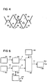
- the first row of teeth formed in the first shell 5 and the second row of teeth formed in the second shell 6 are partially and simplified in FIG 4, wherein the two shells 5 and 6 are not yet fully assembled, and the view of the sensor elements 2 and 3 is shown forth.
- the second row of teeth has a fifth tooth 27 and a sixth tooth 28.
- the row of teeth formed in the first shell 5 with the teeth 20, 21 and 22 and the row of teeth formed in the second shell 6 with the teeth 26, 27 and 28, which are opposite to the teeth 20, 21 and 22 of the first row of teeth form a arranged between the circuit board 4 and the sensor elements 2 and 3 guide means by which the electrical leads 23, 24 and 25 isolated from each other at a certain distance to the circuit board 4 are guided.
- the guide means is adaptable to exacting requirements within the exact design and design within wide limits; for example, the number and mass of the sensor elements used, the shape and wire diameter of the connecting wires, a required quality of the seal around the connecting wires and a required creepage or even dielectric strength between individual connecting wires.
- the two shells 5 and 6 are made of a plastic, in particular certain thermoplastics are advantageous, which hardly absorb moisture.
- the teeth 20, 21, 22, 26, 27 and 28 are formed substantially wedge-shaped.
- the two rows of teeth are designed and arranged in such a way in that a first channel 30 associated with a first connecting wire 23 is delimited by two adjacent teeth 20 and 21 of the first row of teeth and by two adjacent teeth 27 and 26 of the second row of teeth.
- a second channel 31 associated with a second lead wire 24 is bounded by two further adjacent teeth 21 and 22 of the first row of teeth and two further adjacent teeth 26 and 28 of the second row of teeth.
- the cross section of the first channel 30 and the cross section of the second channel 31 decrease more and more, wherein the inserted in the first channel 30 connecting wire and captured in a between the first tooth 20 and the second tooth 21st formed saddle 32 is positioned and wherein also the inserted in the second channel 31 connecting wire is captured and positioned in a formed between the second tooth 21 and the third tooth 22 further saddle 33.
- a steepness of the tooth flanks dependent on a wedge angle ⁇ of the teeth of the second row of teeth or on a wedge angle ⁇ of the teeth of the first row of teeth is chosen to be at least so steep that no self-locking occurs when the connecting wires 23 and 24 are caught.
- the formed between adjacent teeth of a row of teeth saddle 32 or 33 is advantageously adapted to the shape and diameter of the received lead wire 23 and 24, that a certain degree of sealing, between the sensor element 2 or 3 and the circuit board in the assembled state of the two assembled shells 5 and 6 is achieved.
- the guide means on a third row of teeth which is arranged between the second row of teeth and the circuit board 4 and formed on the first shell 5.
- the third row of teeth one seventh tooth 35 (FIG. 2), an eighth tooth 36 and a ninth tooth 37, wherein the lead wire 23 of the first sensor element 2 is between the seventh tooth 35 and the eighth tooth 36, and the lead wire 24 of the second sensor element 3 is between the eighth Tooth 36 and the ninth tooth 37 is located.
- the teeth 35, 36 and 37 of the third row of teeth seen from the sensor elements 2 and 3 are arranged just behind the corresponding teeth 20, 21 and 22 of the first row of teeth and the second row of teeth is in the assembled state of the two shells 5 and 6 between inserted the first and the third row of teeth.
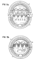
- Fig. 5a and Fig. 5b the two shells 5 and 6 are shown in a view of the sensor elements 2 and 3 ago, wherein the two shells 5 and 6 in Fig. 5a are not yet fully assembled in Fig. 5b ,
- FIG. 5 a the second row of teeth displaced to the rear relative to the first row of teeth is shown with dashed lines - thus invisibly marked - tooth tips of the teeth 27, 26 and 28.
- a tooth 27 or 26 or 28 is exactly behind a corresponding tooth 20 or 21 or 22, wherein the tooth tips of the first row of teeth are directed opposite to the tooth tips of the second row of teeth.
- the two shells 5 and 6 have positioning means by which the two shells 5 and 6 when mating against each other are precisely aligned.
- the second shell 6 has, for example, cams 70 and 71 which, when the two shells 5 and 6 are joined together, are inserted into corresponding holes 72 and 73 recessed on the first shell 5.
- a denotes the distance between the two adjacent lead wires 23 and 24 and b the Distance between the two adjacent leads 24 and 25.
- the distance a or b between two connecting wires is so small that could form on the surface of the two shells 5 and 6 unacceptably high leakage currents between the connecting wires 23 and 24 or 24 and 25, is advantageously at the two shells 5 and 6 design a surface shape such that a significant path for leakage currents is greater than the distance a or b between the connecting wires 23 and 24 or 24 and 25.
- a significant reduction of leakage currents can be achieved by forming a substantially frusto-conical structure 80, 81 and 82 at exit points of the connecting wires 23, 24, 25.
- the two shells 5 and 6 are advantageously matched to the diameter and the shape of the connecting wires 23, 24 and 25 such that a printed circuit board side on the two shells 5 and 6 applied sealant sensor side for creepage currents between the connecting wires 23, 24 and 25 decisive shaping of the guide means is not affected effectively.
- the two shells 5 and 6 are shown completely separated prior to assembly.
- the two shells 5 and 6 by a with Advantage side of the shells 5 and 6 arranged hinge connected to each other, wherein a rotation axis of the hinge is parallel to the lead wires 23, 24 and 25.
- the hinge is formed directly in the integral molding of the two shells 5 and 6.
- a measuring device shown in FIG. 6 has a capacitive humidity sensor 60 and a temperature sensor 61.
- An electrical signal S1 of the humidity sensor 60 is guided to form a humidity signal H with advantage on a connected to the humidity sensor 60 first transducer 62, while an electrical signal S2 of the temperature sensor 61 to form a temperature signal T with advantage on a connected to the temperature sensor 61 second Signal converter 63 is guided.
- the two transducers 62 and 63 are connected to a microprocessor 64.
- a data memory 65 has correction data K for correcting the humidity signal H.
- An output Hr corresponding to the detected relative humidity is calculable by the microprocessor 64 using the humidity signal H, the temperature signal T and the correction data K.
- the output signal Hr is conditioned in an interface unit 66 for a certain communication standard and provided as a standardized output signal Hrs.
- a change in an important sensor characteristic value is detected by a monitoring unit 67 over a relatively long period of time, that is to say over several months or years.
- a change in the ohmic resistance of the humidity sensor 60 is detected by the monitoring unit 67.
- a larger deviation of the resistance value of the capacitive humidity sensor 60 on indicate an error or advanced aging of the humidity sensor 60.
- a status signal ⁇ R is output at an output 68, which is evaluated or forwarded, for example, by the microprocessor 64.
- the status signal ⁇ R is forwarded, for example, as additional information with the output signal Hr or provided in a variant of the measuring device independently of the output signal Hr.
- the signal converters 62 and 63, the microprocessor 64, the data memory 65 are advantageously arranged on the printed circuit board 4 (FIG. 1).
- the interface unit 66 is accommodated on the printed circuit board 4 or in a variant on the side of the sensor tube 8 facing away from the printed circuit board 4 in a further housing.
Landscapes
- Physics & Mathematics (AREA)
- General Physics & Mathematics (AREA)
- Investigating Or Analyzing Materials By The Use Of Electric Means (AREA)
- Measuring Pulse, Heart Rate, Blood Pressure Or Blood Flow (AREA)
- Eye Examination Apparatus (AREA)
- Optical Transform (AREA)
Claims (14)
- Module de capteur doté d'au moins un élément de capteur présentant des fils électriques de connexion et d'un circuit imprimé, les fils électriques de connexion de l'élément de capteur étant raccordés au circuit imprimé de manière électro-conductrice,
un moyen de guidage (20, 21, 22, 26, 27, 28), disposé entre le circuit imprimé (4) et l'élément de capteur (2, 3), étant présent, par l'intermédiaire duquel les fils électriques de connexion (23, 24, 25) sont menés vers le circuit imprimé (4) en étant isolés les uns des autres d'une certaine distance,
le moyen de guidage (20, 21, 22, 26, 27, 28) présentant une première partie et une deuxième partie (26, 27, 28) et les fils de connexion (23, 24, 25) étant disposés entre la première partie (20, 21, 22) et la deuxième partie (26, 27, 28),
caractérisé en ce que la première partie (20, 21, 22) présente des dents (20, 21, 22) de forme essentiellement conique, qui sont exécutées et disposées de telle manière qu'un fil de connexion (23, 24, 25) est situé entre deux dents disposées l'une à côté de l'autre, et
en ce que la deuxième partie (26, 27, 28) présente des dents (26, 27, 28) de forme essentiellement conique, qui sont exécutées et disposées de telle manière que le fil de connexion (23, 24, 25) est situé entre deux dents disposées l'une à côté de l'autre, et
en ce que les dents de la première partie (20, 21, 22) sont disposées de manière décalée par rapport aux dents de la deuxième partie (26, 27, 28). - Module de capteur selon la revendication 1, caractérisé en ce que le moyen de guidage (20, 21, 22, 26, 27, 28), à un point de sortie d'un fil de connexion, présente une forme de surface, par laquelle une trajectoire déterminante pour un courant de fuite entre le fil de connexion et un autre fil de connexion est supérieure à la distance entre les deux fils de connexion.
- Module de capteur selon l'une quelconque des revendications précédentes, caractérisé en ce que deux dents adjacentes (20, 21) de la première partie forment un espace dans lequel est logé un fil de connexion (23), un col (32) de l'espace, sur lequel repose le fil de connexion (23) et duquel part respectivement un flanc de dent des deux dents (20, 21) adjacentes, étant situé dans un plan présentant une couche conductrice du circuit imprimé (4).
- Module de capteur selon l'une quelconque des revendications précédentes, caractérisé en ce que la première partie (20, 21, 22) est formée sur une première coque (5), et en ce que la deuxième partie (26, 27, 28) est formée sur une deuxième coque (6), le circuit imprimé (4) étant fixé au moins à l'une des deux coques (5, 6).
- Module de capteur selon l'une quelconque des revendications précédentes, caractérisé en ce que le circuit imprimé (4) est logé dans la première coque (5).
- Module de capteur selon l'une quelconque des revendications précédentes, caractérisé en ce que les fils de connexion (23, 24, 25) de l'élément de capteur (2, 3) sont soudés au circuit imprimé (4).
- Module de capteur selon l'une quelconque des revendications précédentes, caractérisé en ce que les deux coques (5, 6) sont adaptées de telle manière au diamètre et à la forme des fils de connexion (23, 24, 25) de l'élément de capteur (2, 3) qu'une masse d'étanchéité appliquée du côté du circuit imprimé sur les deux coques (5, 6) n'influence pas essentiellement, du côté du capteur, un façonnage du moyen de guidage (20, 21, 22, 26, 27, 28) déterminant pour des courants de fuite entre les fils de connexion (23, 24, 25).
- Module de capteur selon l'une quelconque des revendications précédentes, caractérisé en ce qu'un montage (62, 63) électronique est placé sur le circuit imprimé (4) pour convertir des signaux électriques de capteur.
- Module de capteur selon l'une quelconque des revendications précédentes, caractérisé en ce qu'une mémoire de données (65) comportant des données (K) est placée sur le circuit imprimé (4) pour corriger des signaux électriques de capteur.
- Module de capteur selon l'une quelconque des revendications précédentes, caractérisé en ce qu'un processeur (64) est disposé sur le circuit imprimé (4), par l'intermédiaire duquel les signaux de capteur sont transformables.
- Module de capteur selon l'une quelconque des revendications précédentes, caractérisé en ce que l'élément de capteur peut être recouvert par un filtre (7).
- Module de capteur selon l'une quelconque des revendications précédentes, caractérisé en ce qu'un tube palpeur (8) recouvrant le circuit imprimé (4) est disposé.
- Module de capteur selon l'une quelconque des revendications précédentes, caractérisé en ce que l'élément de capteur (2, 3) est un capteur d'humidité.
- Module de capteur selon l'une quelconque des revendications précédentes, caractérisé en ce que l'élément de capteur (2, 3) est un capteur de température.
Priority Applications (4)
| Application Number | Priority Date | Filing Date | Title |
|---|---|---|---|
| DE502004001155T DE502004001155D1 (de) | 2004-03-15 | 2004-03-15 | Messeinrichtung |
| AT04006043T ATE335988T1 (de) | 2004-03-15 | 2004-03-15 | Messeinrichtung |
| EP04006043A EP1577648B1 (fr) | 2004-03-15 | 2004-03-15 | Dispositif de mesure |
| US11/080,676 US7345591B2 (en) | 2004-03-15 | 2005-03-15 | Measuring device |
Applications Claiming Priority (1)
| Application Number | Priority Date | Filing Date | Title |
|---|---|---|---|
| EP04006043A EP1577648B1 (fr) | 2004-03-15 | 2004-03-15 | Dispositif de mesure |
Publications (2)
| Publication Number | Publication Date |
|---|---|
| EP1577648A1 EP1577648A1 (fr) | 2005-09-21 |
| EP1577648B1 true EP1577648B1 (fr) | 2006-08-09 |
Family
ID=34833594
Family Applications (1)
| Application Number | Title | Priority Date | Filing Date |
|---|---|---|---|
| EP04006043A Expired - Lifetime EP1577648B1 (fr) | 2004-03-15 | 2004-03-15 | Dispositif de mesure |
Country Status (3)
| Country | Link |
|---|---|
| EP (1) | EP1577648B1 (fr) |
| AT (1) | ATE335988T1 (fr) |
| DE (1) | DE502004001155D1 (fr) |
Cited By (1)
| Publication number | Priority date | Publication date | Assignee | Title |
|---|---|---|---|---|
| US9689719B2 (en) | 2014-10-29 | 2017-06-27 | Siemens Aktiengesellschaft | Cover for a duct sensor |
Families Citing this family (1)
| Publication number | Priority date | Publication date | Assignee | Title |
|---|---|---|---|---|
| EP4067182A1 (fr) * | 2021-02-19 | 2022-10-05 | Transportation IP Holdings, LLC | Ensemble capteur, sécheur et système de commande de véhicule l'utilisant |
Family Cites Families (4)
| Publication number | Priority date | Publication date | Assignee | Title |
|---|---|---|---|---|
| DE4241242C2 (de) * | 1992-12-08 | 1995-01-19 | Honeywell Bv | Elektrischer Zustandsfühler |
| DE19719010C2 (de) * | 1996-05-24 | 2003-04-30 | Ifm Electronic Gmbh | Wärmeübergangskontroll- und/oder -meßgerät |
| DE19938868B4 (de) * | 1999-08-17 | 2005-11-24 | Siemens Ag | Sensoreinrichtung und Verfahren zum Herstellen einer Sensoreinrichtung |
| DE10146156A1 (de) * | 2000-09-20 | 2002-04-04 | Delphi Tech Inc | Modulare Sensoranordnung und Verfahren zur Herstellung derselben |
-
2004
- 2004-03-15 EP EP04006043A patent/EP1577648B1/fr not_active Expired - Lifetime
- 2004-03-15 DE DE502004001155T patent/DE502004001155D1/de not_active Expired - Lifetime
- 2004-03-15 AT AT04006043T patent/ATE335988T1/de active
Cited By (1)
| Publication number | Priority date | Publication date | Assignee | Title |
|---|---|---|---|---|
| US9689719B2 (en) | 2014-10-29 | 2017-06-27 | Siemens Aktiengesellschaft | Cover for a duct sensor |
Also Published As
| Publication number | Publication date |
|---|---|
| EP1577648A1 (fr) | 2005-09-21 |
| DE502004001155D1 (de) | 2006-09-21 |
| ATE335988T1 (de) | 2006-09-15 |
Similar Documents
| Publication | Publication Date | Title |
|---|---|---|
| DE19936300B4 (de) | Druckerkennungsvorrichtung und Druckerkennungsvorrichtung-Anordnung hiermit | |
| EP1202024B1 (fr) | Module de capteur avec une plaque de métal découpée ( capteur magnéto résistif vanne papillon ) | |
| EP2989669A1 (fr) | Procédé de fabrication d'un système de mise en contact électrique de batterie et système de mise en contact électrique de batterie | |
| DE112015002366T5 (de) | Elektronische drosselkörperanordnung | |
| DE102008006542A1 (de) | Batteriezustand-Detektorvorrichtung | |
| DE102007009569B4 (de) | Anschlusseinrichtung und Verfahren zu deren Herstellung | |
| DE112016004799T5 (de) | Leiterelementmodul und Batterieverbund | |
| DE102006019497A1 (de) | Sensorvorrichtung für eine Starterbatterie in einem Kraftfahrzeug | |
| WO2014037354A1 (fr) | Transducteur ultrasonore et procédé de fabrication d'un transducteur ultrasonore | |
| WO2003046496A1 (fr) | Capteur et ensemble de detection | |
| EP4221966A1 (fr) | Procédé de fabrication d'un ensemble constitué d'une partie tube en plastique ayant au moins un insert tube-fils et un connecteur de borne | |
| WO2017194606A2 (fr) | Dispositif de régulation de température, utilisation du dispositif, procédé de fabrication d'un boîtier et boîtier | |
| US7345591B2 (en) | Measuring device | |
| EP1577648B1 (fr) | Dispositif de mesure | |
| DE102013215145A1 (de) | Elektronisches Steuergerät | |
| WO2006048231A1 (fr) | Capteur de courant de batterie pour vehicule automobile | |
| DE10158529A1 (de) | Temperatur sensor | |
| EP2737326B1 (fr) | Circuit de conduction d'un courant électrique | |
| DE112016000903B4 (de) | Motorvorrichtung | |
| EP1353160B1 (fr) | Capteur de pression | |
| DE10158554B4 (de) | Temperatursensor | |
| DE102004056866A1 (de) | Extrudierte Flachleitung sowie Verfahren zum Erzeugen einer extrudierten Flachleitung | |
| WO2009033676A2 (fr) | Module de raccordement, module collecteur de courant et ensemble doté de ces modules pour un collecteur en amont dans une installation photovoltaïque | |
| DE102020112464B4 (de) | Massenstrom-Sensor-Baugruppe sowie Verfahren zur Herstellung einer Massenstrom-Sensor-Baugruppe | |
| DE102007018175A1 (de) | Stromverteiler für Leitungssatz inbesondere in einem Kraftfahrzeug |
Legal Events
| Date | Code | Title | Description |
|---|---|---|---|
| PUAI | Public reference made under article 153(3) epc to a published international application that has entered the european phase |
Free format text: ORIGINAL CODE: 0009012 |
|
| AK | Designated contracting states |
Kind code of ref document: A1 Designated state(s): AT BE BG CH CY CZ DE DK EE ES FI FR GB GR HU IE IT LI LU MC NL PL PT RO SE SI SK TR |
|
| AX | Request for extension of the european patent |
Extension state: AL LT LV MK |
|
| RAP1 | Party data changed (applicant data changed or rights of an application transferred) |
Owner name: SIEMENS SCHWEIZ AG |
|
| 17P | Request for examination filed |
Effective date: 20051021 |
|
| GRAP | Despatch of communication of intention to grant a patent |
Free format text: ORIGINAL CODE: EPIDOSNIGR1 |
|
| AKX | Designation fees paid |
Designated state(s): AT BE BG CH CY CZ DE DK EE ES FI FR GB GR HU IE IT LI LU MC NL PL PT RO SE SI SK TR |
|
| GRAS | Grant fee paid |
Free format text: ORIGINAL CODE: EPIDOSNIGR3 |
|
| GRAA | (expected) grant |
Free format text: ORIGINAL CODE: 0009210 |
|
| AK | Designated contracting states |
Kind code of ref document: B1 Designated state(s): AT BE BG CH CY CZ DE DK EE ES FI FR GB GR HU IE IT LI LU MC NL PL PT RO SE SI SK TR |
|
| PG25 | Lapsed in a contracting state [announced via postgrant information from national office to epo] |
Ref country code: IT Free format text: LAPSE BECAUSE OF FAILURE TO SUBMIT A TRANSLATION OF THE DESCRIPTION OR TO PAY THE FEE WITHIN THE PRESCRIBED TIME-LIMIT;WARNING: LAPSES OF ITALIAN PATENTS WITH EFFECTIVE DATE BEFORE 2007 MAY HAVE OCCURRED AT ANY TIME BEFORE 2007. THE CORRECT EFFECTIVE DATE MAY BE DIFFERENT FROM THE ONE RECORDED. Effective date: 20060809 Ref country code: SK Free format text: LAPSE BECAUSE OF FAILURE TO SUBMIT A TRANSLATION OF THE DESCRIPTION OR TO PAY THE FEE WITHIN THE PRESCRIBED TIME-LIMIT Effective date: 20060809 Ref country code: IE Free format text: LAPSE BECAUSE OF FAILURE TO SUBMIT A TRANSLATION OF THE DESCRIPTION OR TO PAY THE FEE WITHIN THE PRESCRIBED TIME-LIMIT Effective date: 20060809 Ref country code: SI Free format text: LAPSE BECAUSE OF FAILURE TO SUBMIT A TRANSLATION OF THE DESCRIPTION OR TO PAY THE FEE WITHIN THE PRESCRIBED TIME-LIMIT Effective date: 20060809 Ref country code: NL Free format text: LAPSE BECAUSE OF FAILURE TO SUBMIT A TRANSLATION OF THE DESCRIPTION OR TO PAY THE FEE WITHIN THE PRESCRIBED TIME-LIMIT Effective date: 20060809 Ref country code: RO Free format text: LAPSE BECAUSE OF FAILURE TO SUBMIT A TRANSLATION OF THE DESCRIPTION OR TO PAY THE FEE WITHIN THE PRESCRIBED TIME-LIMIT Effective date: 20060809 Ref country code: FI Free format text: LAPSE BECAUSE OF FAILURE TO SUBMIT A TRANSLATION OF THE DESCRIPTION OR TO PAY THE FEE WITHIN THE PRESCRIBED TIME-LIMIT Effective date: 20060809 Ref country code: PL Free format text: LAPSE BECAUSE OF FAILURE TO SUBMIT A TRANSLATION OF THE DESCRIPTION OR TO PAY THE FEE WITHIN THE PRESCRIBED TIME-LIMIT Effective date: 20060809 Ref country code: CZ Free format text: LAPSE BECAUSE OF FAILURE TO SUBMIT A TRANSLATION OF THE DESCRIPTION OR TO PAY THE FEE WITHIN THE PRESCRIBED TIME-LIMIT Effective date: 20060809 |
|
| REG | Reference to a national code |
Ref country code: GB Ref legal event code: FG4D Free format text: NOT ENGLISH |
|
| REG | Reference to a national code |
Ref country code: CH Ref legal event code: EP |
|
| REG | Reference to a national code |
Ref country code: IE Ref legal event code: FG4D Free format text: LANGUAGE OF EP DOCUMENT: GERMAN |
|
| REF | Corresponds to: |
Ref document number: 502004001155 Country of ref document: DE Date of ref document: 20060921 Kind code of ref document: P |
|
| PG25 | Lapsed in a contracting state [announced via postgrant information from national office to epo] |
Ref country code: DK Free format text: LAPSE BECAUSE OF FAILURE TO SUBMIT A TRANSLATION OF THE DESCRIPTION OR TO PAY THE FEE WITHIN THE PRESCRIBED TIME-LIMIT Effective date: 20061109 Ref country code: BG Free format text: LAPSE BECAUSE OF FAILURE TO SUBMIT A TRANSLATION OF THE DESCRIPTION OR TO PAY THE FEE WITHIN THE PRESCRIBED TIME-LIMIT Effective date: 20061109 |
|
| PG25 | Lapsed in a contracting state [announced via postgrant information from national office to epo] |
Ref country code: ES Free format text: LAPSE BECAUSE OF FAILURE TO SUBMIT A TRANSLATION OF THE DESCRIPTION OR TO PAY THE FEE WITHIN THE PRESCRIBED TIME-LIMIT Effective date: 20061120 |
|
| GBT | Gb: translation of ep patent filed (gb section 77(6)(a)/1977) |
Effective date: 20061030 |
|
| REG | Reference to a national code |
Ref country code: SE Ref legal event code: TRGR |
|
| PG25 | Lapsed in a contracting state [announced via postgrant information from national office to epo] |
Ref country code: PT Free format text: LAPSE BECAUSE OF FAILURE TO SUBMIT A TRANSLATION OF THE DESCRIPTION OR TO PAY THE FEE WITHIN THE PRESCRIBED TIME-LIMIT Effective date: 20070109 |
|
| NLV1 | Nl: lapsed or annulled due to failure to fulfill the requirements of art. 29p and 29m of the patents act | ||
| ET | Fr: translation filed | ||
| REG | Reference to a national code |
Ref country code: IE Ref legal event code: FD4D |
|
| PLBE | No opposition filed within time limit |
Free format text: ORIGINAL CODE: 0009261 |
|
| STAA | Information on the status of an ep patent application or granted ep patent |
Free format text: STATUS: NO OPPOSITION FILED WITHIN TIME LIMIT |
|
| 26N | No opposition filed |
Effective date: 20070510 |
|
| BERE | Be: lapsed |
Owner name: SIEMENS SCHWEIZ A.G. Effective date: 20070331 |
|
| PG25 | Lapsed in a contracting state [announced via postgrant information from national office to epo] |
Ref country code: BE Free format text: LAPSE BECAUSE OF NON-PAYMENT OF DUE FEES Effective date: 20070331 |
|
| PG25 | Lapsed in a contracting state [announced via postgrant information from national office to epo] |
Ref country code: MC Free format text: LAPSE BECAUSE OF NON-PAYMENT OF DUE FEES Effective date: 20070331 |
|
| PG25 | Lapsed in a contracting state [announced via postgrant information from national office to epo] |
Ref country code: GR Free format text: LAPSE BECAUSE OF FAILURE TO SUBMIT A TRANSLATION OF THE DESCRIPTION OR TO PAY THE FEE WITHIN THE PRESCRIBED TIME-LIMIT Effective date: 20061110 |
|
| PG25 | Lapsed in a contracting state [announced via postgrant information from national office to epo] |
Ref country code: EE Free format text: LAPSE BECAUSE OF FAILURE TO SUBMIT A TRANSLATION OF THE DESCRIPTION OR TO PAY THE FEE WITHIN THE PRESCRIBED TIME-LIMIT Effective date: 20060809 |
|
| REG | Reference to a national code |
Ref country code: FR Ref legal event code: TP |
|
| REG | Reference to a national code |
Ref country code: CH Ref legal event code: NV Representative=s name: SIEMENS SCHWEIZ AG Ref country code: CH Ref legal event code: PUE Owner name: SIEMENS AKTIENGESELLSCHAFT Free format text: SIEMENS SCHWEIZ AG#ALBISRIEDERSTRASSE 245#8047 ZUERICH (CH) -TRANSFER TO- SIEMENS AKTIENGESELLSCHAFT#WITTELSBACHERPLATZ 2#80333 MUENCHEN (DE) |
|
| REG | Reference to a national code |
Ref country code: GB Ref legal event code: 732E Free format text: REGISTERED BETWEEN 20090514 AND 20090520 |
|
| PG25 | Lapsed in a contracting state [announced via postgrant information from national office to epo] |
Ref country code: CY Free format text: LAPSE BECAUSE OF FAILURE TO SUBMIT A TRANSLATION OF THE DESCRIPTION OR TO PAY THE FEE WITHIN THE PRESCRIBED TIME-LIMIT Effective date: 20060809 Ref country code: LU Free format text: LAPSE BECAUSE OF NON-PAYMENT OF DUE FEES Effective date: 20070315 |
|
| PG25 | Lapsed in a contracting state [announced via postgrant information from national office to epo] |
Ref country code: HU Free format text: LAPSE BECAUSE OF FAILURE TO SUBMIT A TRANSLATION OF THE DESCRIPTION OR TO PAY THE FEE WITHIN THE PRESCRIBED TIME-LIMIT Effective date: 20070210 Ref country code: TR Free format text: LAPSE BECAUSE OF FAILURE TO SUBMIT A TRANSLATION OF THE DESCRIPTION OR TO PAY THE FEE WITHIN THE PRESCRIBED TIME-LIMIT Effective date: 20060809 |
|
| PG25 | Lapsed in a contracting state [announced via postgrant information from national office to epo] |
Ref country code: DE Free format text: LAPSE BECAUSE OF NON-PAYMENT OF DUE FEES Effective date: 20111001 |
|
| REG | Reference to a national code |
Ref country code: CH Ref legal event code: PUE Owner name: SIEMENS SCHWEIZ AG, CH Free format text: FORMER OWNER: SIEMENS AKTIENGESELLSCHAFT, DE |
|
| REG | Reference to a national code |
Ref country code: FR Ref legal event code: PLFP Year of fee payment: 12 |
|
| REG | Reference to a national code |
Ref country code: GB Ref legal event code: 732E Free format text: REGISTERED BETWEEN 20150220 AND 20150225 |
|
| REG | Reference to a national code |
Ref country code: DE Ref legal event code: R081 Ref document number: 502004001155 Country of ref document: DE Owner name: SIEMENS SCHWEIZ AG, CH Free format text: FORMER OWNER: SIEMENS AKTIENGESELLSCHAFT, 80333 MUENCHEN, DE Effective date: 20150407 |
|
| REG | Reference to a national code |
Ref country code: AT Ref legal event code: PC Ref document number: 335988 Country of ref document: AT Kind code of ref document: T Owner name: SIEMENS SCHWEIZ AG, CH Effective date: 20150330 |
|
| REG | Reference to a national code |
Ref country code: FR Ref legal event code: TP Owner name: SIEMENS SCHWEIZ AG, CH Effective date: 20160202 |
|
| REG | Reference to a national code |
Ref country code: FR Ref legal event code: PLFP Year of fee payment: 13 |
|
| REG | Reference to a national code |
Ref country code: FR Ref legal event code: PLFP Year of fee payment: 14 |
|
| REG | Reference to a national code |
Ref country code: FR Ref legal event code: PLFP Year of fee payment: 15 |
|
| PGFP | Annual fee paid to national office [announced via postgrant information from national office to epo] |
Ref country code: FR Payment date: 20230317 Year of fee payment: 20 Ref country code: AT Payment date: 20230207 Year of fee payment: 20 |
|
| PGFP | Annual fee paid to national office [announced via postgrant information from national office to epo] |
Ref country code: SE Payment date: 20230307 Year of fee payment: 20 Ref country code: IT Payment date: 20230321 Year of fee payment: 20 Ref country code: DE Payment date: 20220620 Year of fee payment: 20 |
|
| PGFP | Annual fee paid to national office [announced via postgrant information from national office to epo] |
Ref country code: CH Payment date: 20230612 Year of fee payment: 20 |
|
| PGFP | Annual fee paid to national office [announced via postgrant information from national office to epo] |
Ref country code: GB Payment date: 20230403 Year of fee payment: 20 |
|
| REG | Reference to a national code |
Ref country code: DE Ref legal event code: R071 Ref document number: 502004001155 Country of ref document: DE Ref country code: CH Ref legal event code: PL |
|
| REG | Reference to a national code |
Ref country code: GB Ref legal event code: PE20 Expiry date: 20240314 |
|
| PG25 | Lapsed in a contracting state [announced via postgrant information from national office to epo] |
Ref country code: GB Free format text: LAPSE BECAUSE OF EXPIRATION OF PROTECTION Effective date: 20240314 |
|
| REG | Reference to a national code |
Ref country code: SE Ref legal event code: EUG |
|
| REG | Reference to a national code |
Ref country code: AT Ref legal event code: MK07 Ref document number: 335988 Country of ref document: AT Kind code of ref document: T Effective date: 20240315 |