EP1575023A2 - Flüssigkristall-Anzeigvorrichtung und Verfahren zu deren Ansteuerung - Google Patents
Flüssigkristall-Anzeigvorrichtung und Verfahren zu deren Ansteuerung Download PDFInfo
- Publication number
- EP1575023A2 EP1575023A2 EP05005279A EP05005279A EP1575023A2 EP 1575023 A2 EP1575023 A2 EP 1575023A2 EP 05005279 A EP05005279 A EP 05005279A EP 05005279 A EP05005279 A EP 05005279A EP 1575023 A2 EP1575023 A2 EP 1575023A2
- Authority
- EP
- European Patent Office
- Prior art keywords
- supplemental
- voltage
- pixel electrode
- liquid crystal
- electrode
- Prior art date
- Legal status (The legal status is an assumption and is not a legal conclusion. Google has not performed a legal analysis and makes no representation as to the accuracy of the status listed.)
- Withdrawn
Links
Images




Classifications
-
- G—PHYSICS
- G09—EDUCATION; CRYPTOGRAPHY; DISPLAY; ADVERTISING; SEALS
- G09G—ARRANGEMENTS OR CIRCUITS FOR CONTROL OF INDICATING DEVICES USING STATIC MEANS TO PRESENT VARIABLE INFORMATION
- G09G3/00—Control arrangements or circuits, of interest only in connection with visual indicators other than cathode-ray tubes
- G09G3/20—Control arrangements or circuits, of interest only in connection with visual indicators other than cathode-ray tubes for presentation of an assembly of a number of characters, e.g. a page, by composing the assembly by combination of individual elements arranged in a matrix no fixed position being assigned to or needed to be assigned to the individual characters or partial characters
- G09G3/34—Control arrangements or circuits, of interest only in connection with visual indicators other than cathode-ray tubes for presentation of an assembly of a number of characters, e.g. a page, by composing the assembly by combination of individual elements arranged in a matrix no fixed position being assigned to or needed to be assigned to the individual characters or partial characters by control of light from an independent source
- G09G3/36—Control arrangements or circuits, of interest only in connection with visual indicators other than cathode-ray tubes for presentation of an assembly of a number of characters, e.g. a page, by composing the assembly by combination of individual elements arranged in a matrix no fixed position being assigned to or needed to be assigned to the individual characters or partial characters by control of light from an independent source using liquid crystals
-
- G—PHYSICS
- G09—EDUCATION; CRYPTOGRAPHY; DISPLAY; ADVERTISING; SEALS
- G09G—ARRANGEMENTS OR CIRCUITS FOR CONTROL OF INDICATING DEVICES USING STATIC MEANS TO PRESENT VARIABLE INFORMATION
- G09G3/00—Control arrangements or circuits, of interest only in connection with visual indicators other than cathode-ray tubes
- G09G3/20—Control arrangements or circuits, of interest only in connection with visual indicators other than cathode-ray tubes for presentation of an assembly of a number of characters, e.g. a page, by composing the assembly by combination of individual elements arranged in a matrix no fixed position being assigned to or needed to be assigned to the individual characters or partial characters
- G09G3/34—Control arrangements or circuits, of interest only in connection with visual indicators other than cathode-ray tubes for presentation of an assembly of a number of characters, e.g. a page, by composing the assembly by combination of individual elements arranged in a matrix no fixed position being assigned to or needed to be assigned to the individual characters or partial characters by control of light from an independent source
- G09G3/36—Control arrangements or circuits, of interest only in connection with visual indicators other than cathode-ray tubes for presentation of an assembly of a number of characters, e.g. a page, by composing the assembly by combination of individual elements arranged in a matrix no fixed position being assigned to or needed to be assigned to the individual characters or partial characters by control of light from an independent source using liquid crystals
- G09G3/3611—Control of matrices with row and column drivers
- G09G3/3648—Control of matrices with row and column drivers using an active matrix
-
- G—PHYSICS
- G02—OPTICS
- G02F—OPTICAL DEVICES OR ARRANGEMENTS FOR THE CONTROL OF LIGHT BY MODIFICATION OF THE OPTICAL PROPERTIES OF THE MEDIA OF THE ELEMENTS INVOLVED THEREIN; NON-LINEAR OPTICS; FREQUENCY-CHANGING OF LIGHT; OPTICAL LOGIC ELEMENTS; OPTICAL ANALOGUE/DIGITAL CONVERTERS
- G02F1/00—Devices or arrangements for the control of the intensity, colour, phase, polarisation or direction of light arriving from an independent light source, e.g. switching, gating or modulating; Non-linear optics
- G02F1/01—Devices or arrangements for the control of the intensity, colour, phase, polarisation or direction of light arriving from an independent light source, e.g. switching, gating or modulating; Non-linear optics for the control of the intensity, phase, polarisation or colour
- G02F1/13—Devices or arrangements for the control of the intensity, colour, phase, polarisation or direction of light arriving from an independent light source, e.g. switching, gating or modulating; Non-linear optics for the control of the intensity, phase, polarisation or colour based on liquid crystals, e.g. single liquid crystal display cells
- G02F1/133—Constructional arrangements; Operation of liquid crystal cells; Circuit arrangements
-
- G—PHYSICS
- G09—EDUCATION; CRYPTOGRAPHY; DISPLAY; ADVERTISING; SEALS
- G09G—ARRANGEMENTS OR CIRCUITS FOR CONTROL OF INDICATING DEVICES USING STATIC MEANS TO PRESENT VARIABLE INFORMATION
- G09G2300/00—Aspects of the constitution of display devices
- G09G2300/08—Active matrix structure, i.e. with use of active elements, inclusive of non-linear two terminal elements, in the pixels together with light emitting or modulating elements
- G09G2300/0876—Supplementary capacities in pixels having special driving circuits and electrodes instead of being connected to common electrode or ground; Use of additional capacitively coupled compensation electrodes
-
- G—PHYSICS
- G09—EDUCATION; CRYPTOGRAPHY; DISPLAY; ADVERTISING; SEALS
- G09G—ARRANGEMENTS OR CIRCUITS FOR CONTROL OF INDICATING DEVICES USING STATIC MEANS TO PRESENT VARIABLE INFORMATION
- G09G2320/00—Control of display operating conditions
- G09G2320/04—Maintaining the quality of display appearance
- G09G2320/043—Preventing or counteracting the effects of ageing
-
- G—PHYSICS
- G09—EDUCATION; CRYPTOGRAPHY; DISPLAY; ADVERTISING; SEALS
- G09G—ARRANGEMENTS OR CIRCUITS FOR CONTROL OF INDICATING DEVICES USING STATIC MEANS TO PRESENT VARIABLE INFORMATION
- G09G3/00—Control arrangements or circuits, of interest only in connection with visual indicators other than cathode-ray tubes
- G09G3/20—Control arrangements or circuits, of interest only in connection with visual indicators other than cathode-ray tubes for presentation of an assembly of a number of characters, e.g. a page, by composing the assembly by combination of individual elements arranged in a matrix no fixed position being assigned to or needed to be assigned to the individual characters or partial characters
- G09G3/34—Control arrangements or circuits, of interest only in connection with visual indicators other than cathode-ray tubes for presentation of an assembly of a number of characters, e.g. a page, by composing the assembly by combination of individual elements arranged in a matrix no fixed position being assigned to or needed to be assigned to the individual characters or partial characters by control of light from an independent source
- G09G3/36—Control arrangements or circuits, of interest only in connection with visual indicators other than cathode-ray tubes for presentation of an assembly of a number of characters, e.g. a page, by composing the assembly by combination of individual elements arranged in a matrix no fixed position being assigned to or needed to be assigned to the individual characters or partial characters by control of light from an independent source using liquid crystals
- G09G3/3611—Control of matrices with row and column drivers
- G09G3/3614—Control of polarity reversal in general
-
- G—PHYSICS
- G09—EDUCATION; CRYPTOGRAPHY; DISPLAY; ADVERTISING; SEALS
- G09G—ARRANGEMENTS OR CIRCUITS FOR CONTROL OF INDICATING DEVICES USING STATIC MEANS TO PRESENT VARIABLE INFORMATION
- G09G3/00—Control arrangements or circuits, of interest only in connection with visual indicators other than cathode-ray tubes
- G09G3/20—Control arrangements or circuits, of interest only in connection with visual indicators other than cathode-ray tubes for presentation of an assembly of a number of characters, e.g. a page, by composing the assembly by combination of individual elements arranged in a matrix no fixed position being assigned to or needed to be assigned to the individual characters or partial characters
- G09G3/34—Control arrangements or circuits, of interest only in connection with visual indicators other than cathode-ray tubes for presentation of an assembly of a number of characters, e.g. a page, by composing the assembly by combination of individual elements arranged in a matrix no fixed position being assigned to or needed to be assigned to the individual characters or partial characters by control of light from an independent source
- G09G3/36—Control arrangements or circuits, of interest only in connection with visual indicators other than cathode-ray tubes for presentation of an assembly of a number of characters, e.g. a page, by composing the assembly by combination of individual elements arranged in a matrix no fixed position being assigned to or needed to be assigned to the individual characters or partial characters by control of light from an independent source using liquid crystals
- G09G3/3611—Control of matrices with row and column drivers
- G09G3/3648—Control of matrices with row and column drivers using an active matrix
- G09G3/3659—Control of matrices with row and column drivers using an active matrix the addressing of the pixel involving the control of two or more scan electrodes or two or more data electrodes, e.g. pixel voltage dependant on signal of two data electrodes
-
- G—PHYSICS
- G09—EDUCATION; CRYPTOGRAPHY; DISPLAY; ADVERTISING; SEALS
- G09G—ARRANGEMENTS OR CIRCUITS FOR CONTROL OF INDICATING DEVICES USING STATIC MEANS TO PRESENT VARIABLE INFORMATION
- G09G3/00—Control arrangements or circuits, of interest only in connection with visual indicators other than cathode-ray tubes
- G09G3/20—Control arrangements or circuits, of interest only in connection with visual indicators other than cathode-ray tubes for presentation of an assembly of a number of characters, e.g. a page, by composing the assembly by combination of individual elements arranged in a matrix no fixed position being assigned to or needed to be assigned to the individual characters or partial characters
- G09G3/34—Control arrangements or circuits, of interest only in connection with visual indicators other than cathode-ray tubes for presentation of an assembly of a number of characters, e.g. a page, by composing the assembly by combination of individual elements arranged in a matrix no fixed position being assigned to or needed to be assigned to the individual characters or partial characters by control of light from an independent source
- G09G3/36—Control arrangements or circuits, of interest only in connection with visual indicators other than cathode-ray tubes for presentation of an assembly of a number of characters, e.g. a page, by composing the assembly by combination of individual elements arranged in a matrix no fixed position being assigned to or needed to be assigned to the individual characters or partial characters by control of light from an independent source using liquid crystals
- G09G3/3611—Control of matrices with row and column drivers
- G09G3/3674—Details of drivers for scan electrodes
- G09G3/3677—Details of drivers for scan electrodes suitable for active matrices only
Definitions
- the invention relates to a display device, particularly to a display device having a pixel portion.
- the liquid crystal display device need use a driving method of inversing a potential of a pixel electrode relative to a potential of a common electrode in a predetermined cycle.
- One of such driving methods of the liquid crystal display device is a DC driving method of applying a DC voltage to the common electrode.
- a line inversion driving method of inverting the pixel potential relative to a potential of the common electrode to be applied with a DC voltage in each of horizontal periods has been known.
- This technology is proposed in "Introduction to liquid crystal display engineering," pp. 101-103, written by Yasoji Suzuki and published by the Nikkan Kogyo Shimbun, Ltd., at November 20, 1998. It is noted that one horizontal period means a period of writing an image signal to all the pixel portions arrayed along one gate line.
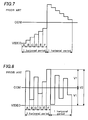
- Fig. 7 shows a waveform chart in a case where a liquid crystal display device is driven by using a conventional line inversion driving method.
- image signals are inverted relative to a potential COM of a common electrode in each of the horizontal periods.
- Each of the image signals is changed in each of pixel portions A to F according to an image to be displayed.
- a liquid crystal display device using a dot inversion driving method of inverting each of image signals relative to a potential COM of a common electrode in each of adjacent pixel portions A to F has been proposed, too.
- Fig. 8 is a waveform chart in a case where a liquid crystal display device is driven by using the conventional dot inversion driving method.
- the liquid crystal display device is driven by using the conventional dot inversion driving method, different from the conventional line inversion driving method shown in Fig. 7, each of the image signals corresponding to the image to be displayed is inverted relative to the potential COM of the common electrode in each of the pixel portions A to F.
- the invention provides a liquid crystal display device that includes a plurality of drain lines, a plurality of gate lines arranged to ran across, preferably substantially normal, to the drain lines, a plurality of pixel electrodes connected to corresponding drain lines, a common electrode, a liquid crystal layer disposed between the pixel electrodes and the common electrode, and a plurality of supplemental capacitors each provided for corresponding pixel electrodes.
- Each of the supplemental capacitors comprises a first electrode connected to a corresponding pixel electrode and a second electrode.
- the device also includes a plurality of supplemental capacitance lines each connected to corresponding second electrodes and configured to receive supplemental voltages, and a correction circuit correcting image signals supplied to the pixel electrodes through the drain lines and the supplemental capacitors when a start voltage that is a voltage of a pixel electrode at a start of receiving a supplemental voltage or an end voltage that is a voltage of the pixel electrode at an end of receiving the supplemental voltage falls within a range of voltage applied to the pixel electrode that corresponds to a change in a capacitance of the liquid crystal.
- the invention also provides a method of controlling a liquid crystal display device.
- the method includes providing a liquid crystal display device that includes a gate line, a first pixel electrode and a second pixel electrode connected to the gate line, a common electrode, a liquid crystal layer disposed between the first and second pixel electrodes and the common electrode, a first supplemental capacitor provided for the first pixel electrode, a second supplemental capacitor provided for the second pixel electrode, a first supplemental capacitance line connected to the first supplemental capacitor and configured to receive a first supplemental voltage, and a second supplemental capacitance line connected to the second supplemental capacitor and configured to receive a second supplemental voltage. supplying the first supplemental voltage to the first supplemental capacitance line after completion of applying an image signal to the first pixel electrode.
- the method also includes supplying the second supplemental voltage to the second supplemental capacitance line after completion of applying another image signal to the second pixel electrode, and performing gamma correction to the another image signal based on a transmittance characteristic of the liquid crystal layer observed during the supplying of the first supplemental voltage.
- Fig. 1 is a plan view of a liquid crystal display device of a first embodiment of the invention.
- a display portion 2 is provided on a substrate 1.
- Pixel portions 3-1a to 3-1d, 3-2a to 3-2d are arrayed on the display portion 2.
- Fig. 1 shows a matrix of two rows and four columns formed of two gate lines G1 and G2, four drain lines D1 to D4 crossing the gate lines G1 and G2, and eight pixel portions 3-1a to 3-1d and 3-2a to 3-2d, for simplifying the drawing.
- a plurality of gate lines and a plurality of drain lines are arrayed crossing each other, and a plurality of pixel portions is arrayed in a matrix of m rows and n columns.
- Each of the pixel portions 3-1a to 3-1d and 3-2a to 3-2d includes a liquid crystal layer 31, a transistor 32, and a supplemental capacitance 33.
- the liquid crystal layer 31 is provided between a pixel electrode 34 and a common electrode 35.
- Drains of the transistors 32 in the pixel portions 3-1a and 3-2a are connected with the drain line D1, and drains of the transistors 32 in the pixel portions 3-1b and 3-2b are connected with the drain line D2.
- drains of the transistors 32 in the pixel portions 3-1c and 3-2c are connected with the drain line D3
- drains of the transistors 32 in the pixel portions 3-1d and 3-2d are connected with the drain line D4.
- Sources in all the pixel portions are connected with the pixel electrodes 34, respectively.
- One electrode 36 of the supplemental capacitance 33 in each of the pixel portions is connected with the pixel electrode 34.
- Another electrodes 37-1a and 37-1c of the supplemental capacitance 33 in the pixel portions 3-1a to 3-1c are connected with the supplemental capacitance line SC1-1, and another electrodes 37-1b and 37-1d of the supplemental capacitance 33 in the pixel portions 3-1b and 3-1d are connected with the supplemental capacitance line SC2-1.
- another electrodes 37-2a and 37-2c of the supplemental capacitance 33 in the pixel portions 3-2a and 3-2c are connected with the supplemental capacitance line SC1-2
- another electrodes 37-2b and 37-2d of the supplemental capacitance 33 in the pixel portions 3-2b and 3-2d are connected with the supplemental capacitance line SC2-2.
- H switches (n-channel transistor) 4a to 4d for driving (scanning) the drain lines D1 to D4 and drain lines in five or more columns (not shown) and an H driver 5 are provided on the substrate 1.
- the H switch 4a corresponding to the pixel portion 3-1a (drain line D1) is connected with an image signal line VIDE01
- the H switch 4b corresponding to the pixel portion 3-1b (drain line D2) is connected with an image signal line VIDE02.
- the H switch denotes an H switch in this embodiment, the H switch can be a transfer gate formed of an H switch and a p-channel transistor or other means.
- a V driver 46 for driving (scanning) the gate line G1 in the first row, the gate line G2 in the second row, and gate lines in the third or more rows (not shown in Fig. 1) is provided on the substrate 1.
- a drive IC 9 is provided outside the substrate 1.
- This drive IC 9 supplies a positive potential HVDD, a negative potential HVSS, a start signal STH, and a clock signal CKH to the H driver 5.
- the IC 9 supplies a positive potential VVDD, a negative potential VVSS, a start signal STV, a clock signal CKV, and an enable signal ENB to the V driver 46.
- the IC 9 supplies a positive potential VSCH, a negative potential VSCL, and a clock signal CKVSC to a potential supply circuit 7.
- Fig. 2 is a timing chart for explaining an operation of the V driver 46 and the potential supply circuit 47 of the liquid crystal display device of the first embodiment.
- a start signal STV of H level is inputted to the V driver 46.
- a clock signal CKV1 turns H level in the V driver 46, and thus a signal of H level is inputted from a shift resister circuit portion 461a (Fig. 3) to an AND circuit portion 462a.
- the clock signal CKV1 turns L level and a clock signal CKV2 turns H level, so that a signal of H level is inputted from the shift resister circuit portion 461b to the And circuit portions 462a and 462b.
- the enable signal ENB turns H level, and thus all the three signals (the signals of the shift resister circuit portions 461a and 461b and the enable signal ENB) inputted to the AND circuit portion 462a become H level. Therefore, a signal of H level is supplied from the AND circuit portion 462a to the gate line G1.
- the enable signal ENB turns L level, so that a signal of L level is supplied from the AND circuit portion 462a to the gate line G1 and the gate line G1 retains L level for one frame period.
- the clock signal CKV2 turns L level.
- the clock signal CKV1 turns H level again, and thus a signal of H level is inputted from the shift resister circuit portion 461c to the AND circuit portions 462b and 462c.
- the enable signal ENB turns H level again, and thus all the three signals (the signals of the shift resister portions 461b and 461c and the enable signal ENB) inputted to the AND circuit portion 462b become H level. Therefore, a signal of H level is supplied from the AND circuit portion 462b to the gate line G2.
- the enable signal ENB turns L level, and thus a signal of L level is supplied from the AND circuit portion 462b to the gate line G2 and the gate line G2 retains L level for one frame period.
- the clock signal CKV1 turns L level.
- the AND circuit portions 462b to 462e for supplying signals to the second or more gate lines sequentially input signals of H level to potential supply circuit portions 47a to 47d.
- a potential supply circuit portion 47a supplies a H level potential VSCH to the supplemental capacitance line SC1-1 and a L level potential VSCL to the supplemental capacitance line SC2-1.
- the H level potential VSCH and the L level potential VSCL are still supplied to the supplemental capacitance line SC1-1 and the supplemental capacitance line SC2-1 respectively, being retained for one frame period.
- the potentials supplied to these supplemental capacitance lines are inverted and retained for one frame period again.
- the potential supply circuit portions 47b to 47d shown in Fig. 3 also perform the same operation as that of the potential supply circuit portion 47a.
- the high level potentials VSCH and the low level potentials VSCL from the potential supply circuit portions 47a to 47d are sequentially supplied to the supplemental capacitance lines SC1-1 to SC1-4 and the supplemental capacitance lines SC2-1 to SC2-4 respectively, at the same timings as the timings of the H level signals supplied to the gate lines G2 to G5.
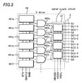
- Fig. 3 is a block diagram of the V driver 46 shown in Fig. 1.
- the V driver 46 has the shift resister circuits portions 461a to 461f, the AND circuit portions 462a to 462e each having three input terminals and one output terminal, and the potential supply circuits 47a to 47d.
- the input terminal of the AND circuit portion 462a is inputted with the output signals of the shift resister circuit portions 461a and 461b and the enable signal ENB.
- Each of the AND circuit portions 462b and the following AND circuit portions is also inputted with the output signals of the two shift resister circuit portions shifted by one portion from the previous shift resister circuit portions and the enable signal ENB.
- the output terminals of the AND circuit portions 462a to 462e are connected with the gate lines G1 to G5, respectively.
- the V driver 46 has the potential supply circuit 47 therein, and the potential supply circuit 47 has the potential supply circuit portions 47a to 47d.
- the potential supply circuit portions 47a to 47d are provided corresponding to the gate lines G1 to G4, respectively.
- the potential supply circuit portion corresponding to the gate line G5 is not shown for simplification of the drawing.
- the potential supply circuit portion 47a corresponding to G1 is inputted with the output signal of the AND circuit portion 462b the output terminal of which is connected with the gate line G2. That is, in this embodiment, the potential supply circuit portion connected with the supplemental capacitance line corresponding to a predetermined gate line is inputted with the output signal of the AND circuit portion the output terminal of which is connected with the next gate line. Furthermore, each of the potential supply circuit portions 47b to 47d has the same circuit structure as that of the potential supply circuit portion 47a.
- the supplemental capacitance lines SC1-1 and SC2-1 are connected with the potential supply circuit portion 47a, and the supplemental capacitance lines SC1-2 and SC2-2 are connected with the potential supply circuit portion 47b.
- These potential supply circuit portions 47a and 47b have functions of supplying the H level potential VSCH and the L level potential VSCL to the supplemental capacitance lines SC1-1 and SC2-1, and SC1-2 and SC2-2, respectively, alternately in each of one frame periods. It is noted that one frame period means a period of writing image signals to all the pixel portions forming the display portion 2.
- the shift resister portion 461 has a function of driving the potential supply circuit 47 so as to sequentially supply signals from the potential supply circuit 47 to a pair of the supplemental capacitance lines SC1-1 and SC2-1 along the first gate line G1 to a pair of supplemental capacitance lines (not shown) along the last gate line.
- the potential of the supplemental capacitance line is changed by ⁇ V after the image signal is inputted to the pixel electrode 34.
- the potential of the pixel electrode 34 which is at the same potential as the electrode 36 of the supplemental capacitance 33, changes by the amount of (C SC /C ALL ) ⁇ V, so that a voltage applied between the pixel electrode 34 and the common electrode 35, that is, a voltage applied to the liquid crystal layer, changes.
- a display can be made even with an image signal of low potential by using a supplemental capacitance coupling, thereby lowering voltages.
- C ALL means all the capacitance in the pixel, and is a sum of the capacitance C SC of the supplemental capacitance 33, the liquid crystal capacitance C LC , and other capacitances in the pixel (e.g. parasitic capacitance).
- the dielectric constant of the liquid crystal changes when a voltage is applied to the liquid crystal, and thus the liquid crystal capacitance changes. Therefore, even when the potential of the supplemental capacitance line is changed by ⁇ V, sometimes the potential of the pixel electrode 34 do not change by (C SC /C ALL ) ⁇ V.
- This is shown as the liquid crystal capacitance as a function of the voltage (C-V curve) in Fig. 4. That is, the liquid crystal capacitance C LC changes by the change of the potential of the supplemental capacitance line when at least one of voltages of the pixel electrode 34 for the common electrode 35 before or after the potential of the supplemental capacitance line is changed lies within a transition region R.
- the transition region R is a region of voltages in which the liquid crystal capacitance C LC largely changes.
- C LC which is one of components of C ALL of the amount (C SC /C ALL ) ⁇ V of potential change of the pixel electrode 34 caused by the potential change of the supplemental capacitance line, changes. Therefore, by correcting the image signal by adding the changing amount of the potential of the pixel electrode 34 using C ALL including the changed C LC , a smooth grayscale image can be realized and a high quality display can be obtained.
- the transition region R is set from a voltage starting the change of the liquid crystal capacitance C LC to a voltage ending the change.
- the changing amounts at the start and the end are small and have a little influence on the display, so that the transition region can be set as a range of voltages providing the changing amounts of 10% or more and less than 90%, at least.
- a correction circuit 19 compensates the image signal with (C SC /C ALL ) ⁇ V corresponding to the liquid crystal capacitance C LC at the end of the changing.
- Fig. 1 shows the correction circuit 19 disposed in the substrate 1, but it is preferable that the compensation is performed in the drive IC 9 and so on outride the substrate 1. More preferably, the compensation is performed in a gamma correction circuit (not shown) built in the drive IC 9 and so on.
- a smooth grayscale display can be obtained by a driving method of changing the potential of the pixel electrode after the image signal is supplied thereto, as described above. This can realize a high quality display and reduce power consumption.
- the potential supply circuit 47 is set in the V driver 46 and the potential supply circuit portions 47a to 47d are sequentially driven by using signals for sequentially driving the gate lines G2 to G5, a circuit size can be reduced and a yield can be improved.
- the potential supply circuit portion corresponding to the predetermined gate line is driven by inputting an output signal of the AND circuit portion, the output terminal of which is connected with the next gate line, to the potential supply circuit portion corresponding to the predetermined gate line. Therefore, the output signal from the next shift resister circuit portion to the predetermined portion is outputted after the output signal of the shift resister circuit portion for driving the predetermined gate line is outputted. Accordingly, either the H level potential VSCH or the L level potential VSCL can be easily supplied to each of the pair of the supplemental capacitance lines corresponding to the predetermined gate line after the completion of writing the image signal to the pixel portions arrayed along the predetermined gate line.
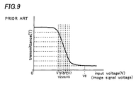
- an input voltage to a pixel electrode is almost equal to an effective voltage to the liquid crystal layer.
- the potential of the pixel electrode itself is changed by changing the potential of the supplemental capacitance line after the image signal is inputted to the pixel electrode, and the liquid crystal capacitance is also changed by the change of the potential of the pixel electrode. Therefore, the input voltage to the pixel electrode is different from the effective voltage applied to the liquid crystal layer, and it is difficult to measure the effective voltage finally applied to the liquid crystal layer although it is possible to calculate the effective voltage. Since a calculated value differs among setting methods of C ALL , the accuracy lowers.
- this embodiment uses a gamma correction circuit performing gamma correction by relying on the relation between an input voltage applied to the liquid crystal layer before the potential of the supplemental capacitance line is changed and a transmittance of the liquid crystal finally obtained after the potential of the pixel electrode is changed using the supplemental capacitance coupling, without using the effective voltage to the liquid crystal.
- This gamma correction circuit can be provided either inside or outside the substrate. The structure and the driving method thereof are the same as those of the first embodiment.
- Fig. 5 shows the transmittance of the liquid crystal as a function of the applied voltage.
- an x axis shows the input voltage for the pixel electrode
- a y axis shows the transmittance of the liquid crystal finally obtained when the potential of the supplemental capacitance line is changed after the signal of the potential of the input voltage is supplied to the pixel electrode.
- a solid line shows the relation between the input voltage and the transmittance in this embodiment
- a dotted line shows the relation between the input voltage and the transmittance when the conventional driving method is used in a display device using a liquid crystal layer made of the same liquid crystal material as that of the embodiment.
- a curve in this embodiment is more relaxed. Therefore, by performing gamma correction with the curve shown in Fig. 5, voltage differences between grayscales increase, so that the grayscales can be displayed more accurately and multiple grayscale images can be obtained.
- This invention is not limited to the above embodiment.
- another shift resister 8 supplying signals to the plurality of supplemental capacitance lines sequentially can be provided as shown in Fig. 6.
- this embodiment shows the case where two image signal lines are provided, the invention can have a structure where one image signal line is provided connecting with all the drain lines.
Landscapes
- Physics & Mathematics (AREA)
- Engineering & Computer Science (AREA)
- General Physics & Mathematics (AREA)
- Crystallography & Structural Chemistry (AREA)
- Chemical & Material Sciences (AREA)
- Theoretical Computer Science (AREA)
- Computer Hardware Design (AREA)
- Nonlinear Science (AREA)
- Mathematical Physics (AREA)
- Optics & Photonics (AREA)
- Control Of Indicators Other Than Cathode Ray Tubes (AREA)
- Liquid Crystal (AREA)
- Liquid Crystal Display Device Control (AREA)
Applications Claiming Priority (2)
| Application Number | Priority Date | Filing Date | Title |
|---|---|---|---|
| JP2004067895A JP4596797B2 (ja) | 2004-03-10 | 2004-03-10 | 液晶表示装置及びその制御方法 |
| JP2004067895 | 2004-03-10 |
Publications (1)
| Publication Number | Publication Date |
|---|---|
| EP1575023A2 true EP1575023A2 (de) | 2005-09-14 |
Family
ID=34824587
Family Applications (1)
| Application Number | Title | Priority Date | Filing Date |
|---|---|---|---|
| EP05005279A Withdrawn EP1575023A2 (de) | 2004-03-10 | 2005-03-10 | Flüssigkristall-Anzeigvorrichtung und Verfahren zu deren Ansteuerung |
Country Status (6)
| Country | Link |
|---|---|
| US (1) | US7564437B2 (de) |
| EP (1) | EP1575023A2 (de) |
| JP (1) | JP4596797B2 (de) |
| KR (1) | KR100702096B1 (de) |
| CN (1) | CN100414413C (de) |
| TW (1) | TWI280540B (de) |
Cited By (1)
| Publication number | Priority date | Publication date | Assignee | Title |
|---|---|---|---|---|
| EP1918905A1 (de) * | 2006-10-24 | 2008-05-07 | Samsung Electronics Co., Ltd. | Anzeigevorrichtung und Verfahren zu ihrer Ansteuerung |
Families Citing this family (7)
| Publication number | Priority date | Publication date | Assignee | Title |
|---|---|---|---|---|
| KR101136282B1 (ko) * | 2005-06-30 | 2012-04-19 | 엘지디스플레이 주식회사 | 액정표시장치 |
| US8154494B2 (en) * | 2006-01-06 | 2012-04-10 | Canon Kabushiki Kaisha | Image display device with liquid crystal modulation elements |
| KR101219043B1 (ko) * | 2006-01-26 | 2013-01-07 | 삼성디스플레이 주식회사 | 표시 장치 및 그 구동 장치 |
| CN100388491C (zh) * | 2006-03-13 | 2008-05-14 | 友达光电股份有限公司 | 显示器电路结构 |
| US7675498B2 (en) * | 2006-07-20 | 2010-03-09 | Tpo Displays Corp. | Dot-inversion display devices and driving method thereof with low power consumption |
| KR101393638B1 (ko) * | 2006-10-24 | 2014-05-26 | 삼성디스플레이 주식회사 | 표시 장치 및 그의 구동 방법 |
| US11120764B2 (en) * | 2017-12-21 | 2021-09-14 | Semiconductor Energy Laboratory Co., Ltd. | Display device and electronic device |
Family Cites Families (7)
| Publication number | Priority date | Publication date | Assignee | Title |
|---|---|---|---|---|
| JP3229156B2 (ja) * | 1995-03-15 | 2001-11-12 | 株式会社東芝 | 液晶表示装置 |
| JP3305240B2 (ja) * | 1997-10-23 | 2002-07-22 | キヤノン株式会社 | 液晶表示パネル駆動装置と駆動方法 |
| CN1394320A (zh) * | 2000-10-27 | 2003-01-29 | 松下电器产业株式会社 | 显示器件 |
| JP2002333870A (ja) * | 2000-10-31 | 2002-11-22 | Matsushita Electric Ind Co Ltd | 液晶表示装置、el表示装置及びその駆動方法、並びに副画素の表示パターン評価方法 |
| TW550531B (en) * | 2002-02-07 | 2003-09-01 | Chi Mei Optoelectronics Corp | Pixel driving device of liquid crystal display |
| JP3627710B2 (ja) * | 2002-02-14 | 2005-03-09 | セイコーエプソン株式会社 | 表示駆動回路、表示パネル、表示装置及び表示駆動方法 |
| JP2003295157A (ja) * | 2002-03-29 | 2003-10-15 | Matsushita Electric Ind Co Ltd | 液晶表示装置 |
-
2004
- 2004-03-10 JP JP2004067895A patent/JP4596797B2/ja not_active Expired - Lifetime
- 2004-12-29 TW TW093141072A patent/TWI280540B/zh not_active IP Right Cessation
-
2005
- 2005-03-09 KR KR1020050019459A patent/KR100702096B1/ko not_active Expired - Fee Related
- 2005-03-09 US US11/074,942 patent/US7564437B2/en active Active
- 2005-03-10 CN CNB2005100537440A patent/CN100414413C/zh not_active Expired - Fee Related
- 2005-03-10 EP EP05005279A patent/EP1575023A2/de not_active Withdrawn
Cited By (2)
| Publication number | Priority date | Publication date | Assignee | Title |
|---|---|---|---|---|
| EP1918905A1 (de) * | 2006-10-24 | 2008-05-07 | Samsung Electronics Co., Ltd. | Anzeigevorrichtung und Verfahren zu ihrer Ansteuerung |
| US8164562B2 (en) | 2006-10-24 | 2012-04-24 | Samsung Electronics Co., Ltd. | Display device and driving method thereof |
Also Published As
| Publication number | Publication date |
|---|---|
| JP2005257931A (ja) | 2005-09-22 |
| TWI280540B (en) | 2007-05-01 |
| CN100414413C (zh) | 2008-08-27 |
| CN1667478A (zh) | 2005-09-14 |
| US20050212743A1 (en) | 2005-09-29 |
| US7564437B2 (en) | 2009-07-21 |
| KR20060043558A (ko) | 2006-05-15 |
| KR100702096B1 (ko) | 2007-04-02 |
| TW200532619A (en) | 2005-10-01 |
| JP4596797B2 (ja) | 2010-12-15 |
Similar Documents
| Publication | Publication Date | Title |
|---|---|---|
| KR100323117B1 (ko) | 액정표시장치의구동회로및액정표시장치 | |
| KR101318043B1 (ko) | 액정표시장치 및 그 구동방법 | |
| KR101415565B1 (ko) | 표시 장치 | |
| RU2443071C1 (ru) | Дисплейное устройство и способ для возбуждения дисплейного устройства | |
| US8866717B2 (en) | Display device and drive method providing improved signal linearity | |
| JP2000310767A (ja) | 液晶表示装置及びその駆動方法 | |
| US8416175B2 (en) | Liquid crystal display device and method for driving the same | |
| KR100668544B1 (ko) | 액정 표시 장치 | |
| KR20090093797A (ko) | 전기 광학 장치, 구동 방법 및 전자 기기 | |
| KR100389027B1 (ko) | 액정표시장치 및 그 구동방법 | |
| EP1575023A2 (de) | Flüssigkristall-Anzeigvorrichtung und Verfahren zu deren Ansteuerung | |
| KR101556778B1 (ko) | 액정 표시 장치 및 그것의 구동 방법 | |
| US8791895B2 (en) | Liquid crystal display device and drive method therefor | |
| JP2000322031A (ja) | 液晶表示装置 | |
| US20100118016A1 (en) | Video voltage supplying circuit, electro-optical apparatus and electronic apparatus | |
| KR100496543B1 (ko) | 액정 표시 장치 및 그 구동 방법 | |
| CN101939779B (zh) | 液晶显示装置的驱动电路 | |
| US20110001743A1 (en) | Drive circuit, drive method, liquid crystal display panel, liquid crystal module, and liquid cystal display device | |
| JPH0973065A (ja) | 液晶駆動方法 | |
| KR100931488B1 (ko) | 액정표시패널 | |
| KR100389023B1 (ko) | 액정표시장치의 감마전압 보정 방법 및 장치 | |
| CN113870806A (zh) | 用于双闸极显示器的补偿系统和方法 | |
| KR20040048523A (ko) | 2도트 인버젼 액정 표시 장치의 구동 방법 및 장치 | |
| KR101432568B1 (ko) | 2도트 인버젼 액정표시장치의 구동 장치 및 방법 | |
| KR20050055159A (ko) | 액정표시장치 및 그 구동방법 |
Legal Events
| Date | Code | Title | Description |
|---|---|---|---|
| PUAI | Public reference made under article 153(3) epc to a published international application that has entered the european phase |
Free format text: ORIGINAL CODE: 0009012 |
|
| AK | Designated contracting states |
Kind code of ref document: A2 Designated state(s): AT BE BG CH CY CZ DE DK EE ES FI FR GB GR HU IE IS IT LI LT LU MC NL PL PT RO SE SI SK TR |
|
| AX | Request for extension of the european patent |
Extension state: AL BA HR LV MK YU |
|
| STAA | Information on the status of an ep patent application or granted ep patent |
Free format text: STATUS: THE APPLICATION HAS BEEN WITHDRAWN |
|
| 18W | Application withdrawn |
Effective date: 20070326 |