EP1569495A1 - Vorrichtung und System einer opto-elektronischen integrierten Schaltung und darauf basierendes Übertragungsverfahren - Google Patents
Vorrichtung und System einer opto-elektronischen integrierten Schaltung und darauf basierendes Übertragungsverfahren Download PDFInfo
- Publication number
- EP1569495A1 EP1569495A1 EP05250983A EP05250983A EP1569495A1 EP 1569495 A1 EP1569495 A1 EP 1569495A1 EP 05250983 A EP05250983 A EP 05250983A EP 05250983 A EP05250983 A EP 05250983A EP 1569495 A1 EP1569495 A1 EP 1569495A1
- Authority
- EP
- European Patent Office
- Prior art keywords
- opto
- integrated circuit
- input
- optical signal
- electronic integrated
- Prior art date
- Legal status (The legal status is an assumption and is not a legal conclusion. Google has not performed a legal analysis and makes no representation as to the accuracy of the status listed.)
- Withdrawn
Links
Images


Classifications
-
- B—PERFORMING OPERATIONS; TRANSPORTING
- B26—HAND CUTTING TOOLS; CUTTING; SEVERING
- B26D—CUTTING; DETAILS COMMON TO MACHINES FOR PERFORATING, PUNCHING, CUTTING-OUT, STAMPING-OUT OR SEVERING
- B26D7/00—Details of apparatus for cutting, cutting-out, stamping-out, punching, perforating, or severing by means other than cutting
- B26D7/18—Means for removing cut-out material or waste
- B26D7/1818—Means for removing cut-out material or waste by pushing out
-
- H—ELECTRICITY
- H04—ELECTRIC COMMUNICATION TECHNIQUE
- H04Q—SELECTING
- H04Q11/00—Selecting arrangements for multiplex systems
- H04Q11/0001—Selecting arrangements for multiplex systems using optical switching
- H04Q11/0005—Switch and router aspects
-
- H—ELECTRICITY
- H10—SEMICONDUCTOR DEVICES; ELECTRIC SOLID-STATE DEVICES NOT OTHERWISE PROVIDED FOR
- H10W—GENERIC PACKAGES, INTERCONNECTIONS, CONNECTORS OR OTHER CONSTRUCTIONAL DETAILS OF DEVICES COVERED BY CLASS H10
- H10W90/00—Package configurations
- H10W90/20—Configurations of stacked chips
- H10W90/293—Configurations of stacked chips characterised by non-galvanic coupling between the chips, e.g. capacitive coupling
-
- B—PERFORMING OPERATIONS; TRANSPORTING
- B26—HAND CUTTING TOOLS; CUTTING; SEVERING
- B26F—PERFORATING; PUNCHING; CUTTING-OUT; STAMPING-OUT; SEVERING BY MEANS OTHER THAN CUTTING
- B26F1/00—Perforating; Punching; Cutting-out; Stamping-out; Apparatus therefor
- B26F1/38—Cutting-out; Stamping-out
- B26F1/40—Cutting-out; Stamping-out using a press, e.g. of the ram type
-
- H—ELECTRICITY
- H04—ELECTRIC COMMUNICATION TECHNIQUE
- H04Q—SELECTING
- H04Q11/00—Selecting arrangements for multiplex systems
- H04Q11/0001—Selecting arrangements for multiplex systems using optical switching
- H04Q11/0005—Switch and router aspects
- H04Q2011/0052—Interconnection of switches
- H04Q2011/0058—Crossbar; Matrix
-
- H—ELECTRICITY
- H10—SEMICONDUCTOR DEVICES; ELECTRIC SOLID-STATE DEVICES NOT OTHERWISE PROVIDED FOR
- H10W—GENERIC PACKAGES, INTERCONNECTIONS, CONNECTORS OR OTHER CONSTRUCTIONAL DETAILS OF DEVICES COVERED BY CLASS H10
- H10W90/00—Package configurations
- H10W90/701—Package configurations characterised by the relative positions of pads or connectors relative to package parts
- H10W90/721—Package configurations characterised by the relative positions of pads or connectors relative to package parts of bump connectors
- H10W90/724—Package configurations characterised by the relative positions of pads or connectors relative to package parts of bump connectors between a chip and a stacked insulating package substrate, interposer or RDL
Definitions
- the present invention relates to an opto-electronic integrated circuit device, an opto-electronic integrated circuit system and a transmission method using the opto-electronic integrated circuit system.
- opto-electronic integrated circuit devices each including optical elements and electronic devices integrated on a substrates are proposed.
- the elements for converting electric signals to optical signals are, e.g. , laser diodes, etc.
- the elements for converting optical signals to electric signals are, e.g., photodiodes, etc.
- the optical elements are interconnected by optical fibers, etc.
- the electronic devices are interconnected by electric interconnections.
- Such opto-electronic integrated circuit device which includes optical elements and electronic devices mounted on one and the same substrate, can be generally downsized and integrated.
- N is a natural number of 2 or more
- opto-electronic integrated circuit devices thus proposed are arranged, and optical signals are transmitted among these opto-electronic integrated circuit devices
- N ⁇ (N-1)/2 optical interconnections are necessary.
- (N-1) laser diodes and (N-1) photodiodes must be provided on each opto-electronic integrated circuit devices. Accordingly, it is not easy to form a system which enables the transmission of optical signals among a number of opto-electronic integrated circuit devices, and even when such system is formed, the system will be bulky.
- an opto-electronic integrated circuit device comprising: an optical switch disposed in an input port of a first input/output port over a substrate, and changing over an optical path of an optical signal inputted from the input port and outputting the optical signal from any one of a plurality of output terminals; an opto-electric conversion element optically connected to one of the plural output terminals of the optical switch, and converting the optical signal outputted from said one output terminal of the optical switch to an electric signal and inputting the converted electric signal into the a semiconductor element mounted over the substrate; and an optical waveguide optically connected to another of the plural output terminal of the optical switch, and outputting the optical signal outputted from said another output terminal of the optical switch through an output port of a second input/output port over the substrate.
- an opto-electronic integrated circuit system comprising a plurality of opto-electronic integrated circuit devices arranged in a matrix, each opto-electronic integrated circuit device including an optical switch disposed in an input port of a first input/output port over a substrate, and changing over an optical path of an optical signal inputted from the input port and outputting the optical signal from any one of a plurality of output terminals; an opto-electric conversion element optically connected to one of the plural output terminals of the optical switch, and converting the optical signal outputted from said one output terminal of the optical switch to an electric signal and inputting the converted electric signal into a semiconductor element mounted over the substrate; an optical waveguide optically connected to another of the plural output terminal of the optical switch, and outputting the optical signal outputted from said another output terminal of the optical switch through an output port of a second input/output port over the substrate; an electric-optic conversion element converting an electric signal outputted from the semiconductor element to an optical
- a transmission method using an opto-electronic integrated circuit system comprising a plurality of opto-electronic integrated circuit device arranged in a matrix, each opto-electronic integrated circuit device including an optical switch disposed in an input port of a first input/output port over a substrate, and changing over an optical path of an optical signal inputted from the input port and outputting the optical signal from any one of a plurality of output terminals; an opto-electric conversion element optically connected to one of the plural output terminals of the optical switch, and converting the optical signal outputted from said one output terminal of the optical switch to an electric signal and inputting the converted electric signal into the a semiconductor element mounted over the substrate; an optical waveguide optically connected to another of the plural output terminal of the optical switch, and outputting the optical signal outputted from said another output terminal of the optical switch through an output port of a second input/output port over the substrate; an electric-optic conversion element converting an electric signal outputted
- a transmission method using an opto-electronic integrated circuit system comprising a plurality of opto-electronic integrated circuit device arranged in a matrix, each opto-electronic integrated circuit device including an optical switch disposed in an input port of a first input/output port over a substrate, and changing over an optical path of an optical signal inputted from the input port and outputting the optical signal from any one of a plurality of output terminals; an opto-electric conversion element optically connected to one of the plural output terminals of the optical switch, and converting the optical signal outputted from said one output terminal of the optical switch to an electric signal and inputting the converted electric signal into the a semiconductor element mounted over the substrate; an optical waveguide optically connected to another of the plural output terminal of the optical switch, and outputting the optical signal outputted from said another output terminal of the optical switch to an output port of a second input/output port over the substrate; an electric-optic conversion element converting an electric signal outputted
- the inputted optical signal when an optical signal inputted to one opto-electronic integrated circuit device is to be processed by said one opto-electronic integrated circuit the optical signal has been inputted to, the inputted optical signal can be converted to an electric signal and inputted to the semiconductor chip or others.
- the optical switch is changed over, and the inputted optical signal can be transmitted as it is to said another opto-electronic integrated circuit device.
- the optical signal when an optical signal is to be processed by said another opto-electronic integrated circuit device, the optical signal is not converted to an electric signal and from the electric signal by the opto-electronic integrated circuit device the optical signal has been inputted to, which can prevent the decrease of the transmission speed.
- the delay of the signal can be prevented, and the opto-electronic integrated circuit system can be small-sized.
- the optical signal when an optical signal is transmitted via a number of opto-electronic integrated circuit devices, the optical signal is converted to an electric signal and converted to the optical signal by the opto-electronic integrated circuit devices the optical signal passes through in the transmission and is outputted, whereby the attenuated optical signal can be amplified.
- the present invention can provide the large-scale opto-electronic integrated circuit system wherein an optical signal passes through a number of the opto-electronic integrated circuit devices.
- the opto-electronic integrated circuit when an optical signal inputted to an opto-electronic integrated circuit is to be processed by another opto-electronic integrated circuit, the opto-electronic integrated circuit the optical signal has been inputted to need not convert the optical signal to an electric signal or the electric signal to the optical signal, which can decrease the load of the processing of the opto-electronic integrated circuit devices to be decreased.
- the opto-electronic integrated circuit device when an optical signal inputted to an opto-electronic integrated circuit is to be processed by another opto-electronic integrated circuit, the opto-electronic integrated circuit device the optical signal has been inputted to does not convert the optical signal to an electric signal and the electric signal to the optical signal, which can decrease the electric power consumption.
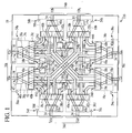
- FIG. 1 is a plan view of the opto-electronic integrated circuit device according to the present embodiment.
- FIG. 2 is a sectional view of the opto-electronic integrated circuit device according to the present embodiment.
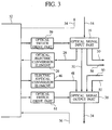
- FIG. 3 is a circuit diagram of a part of the opto-electronic integrated circuit device according to the present embodiment.
- optical waveguides 14 are provided respectively in input ports 12a - 12d on a substrate 10.
- the substrate 10 is, e.g., a silicon substrate, a ceramic substrate, a resin substrate (printed circuit board) or others.
- the optical waveguides 14 are for inputting optical signals from the outside.
- Optical signal input parts 16a - 16d are connected respectively to the optical waveguides 14.
- the optical signal input parts 16a - 16d each comprise a combination of a plurality of optical switches 18a - 18c.
- Each optical switch 18 outputs an optical signal inputted from one input terminal to either of 2 output terminals.
- the optical input parts 16a - 16d each comprise the optical switches 18 cascade connected in two stages.
- the output terminal of the optical switch 18a in the first stage is optically connected to the input terminals of the optical switches 18b, 18c in the second stage by optical waveguides 20.
- An optical signal inputted to the input terminal of the optical switch 18a in the first stage is outputted from either of the two output terminals of the optical switch 18a in the first stage to be inputted to the input terminal of one of the two optical switches 18b, 18c in the second stage.
- the optical signal inputted to the input terminal of said one of the optical switch 18b, 18c in the second stage is outputted from either of the two output terminals of said one of the optical switch 18b, 18c in the second stage.
- Two optical switches 18b, 18c are provided in the second stage, and the total number of the output terminals of the optical switches 18b, 18c in the second stage is four. Accordingly, an optical signal inputted to the one input terminal (input end) 22 of the optical signal input part 16a is outputted from either of the four output terminals (output ends) 24a - 24d of the optical signal input part.
- Opto-electric conversion elements 26a - 26d are provided respectively for the optical signal input parts 12a - 12d. Opto-electric conversion elements 26a - 26d are connected to the output terminals 24a of the optical signal input parts 16a - 16d via optical waveguides 28. Optical signals outputted from the output terminals 24a of the optical signal input parts 16a - 16d are inputted to the opto-electric conversion elements 26a - 26d via the optical waveguides 28 to be converted to electric signals by the opto-electric conversion elements 26a - 26d.
- a semiconductor chip (semiconductor element) 30 is mounted on the substrate 10 (see FIG. 2).
- the semiconductor chip 30 is connected to an electrode (not illustrated) formed on the substrate by means of, e.g., solder bumps 31.
- an electrode not illustrated
- the output terminals (not illustrated) of the opto-electric conversion elements 26a - 26d are electrically connected to the input terminals (not illustrated) of the semiconductor chip 30 by means of electric interconnections (not illustrated).
- the output terminal of the opto-electric conversion element 26a and the output terminal of the semiconductor chip 30 may be interconnected by a solder bump or others.
- Optical signals inputted to the opto-electric conversion elements 26a - 26d are converted to electric signals by the opto-electric conversion elements 26a - 26d to be inputted to the semiconductor chip 30. It is possible that optical signals inputted to the opto-electric conversion elements 26a - 26d are converted to electric signals by the opto-electric conversion elements 26a - 26d to be inputted further to other semiconductor elements (not illustrated), etc. provided on the substrate 10.
- Optical waveguides 34 are formed respectively in output ports 32a - 32d on the substrate 10.
- the optical waveguides 34 are for outputting optical signals to the outside.
- the input ports 12a - 12d and the output ports 32a - 32d constitute input/output ports 36a - 36d.
- Optical output parts 38a - 38d are connected to the optical waveguides 34.
- Each optical output part 38a - 38d comprises a combination of a plurality of optical switches 40a - 40c.
- Each optical switch 40a - 40c outputs an optical signal inputted to either of two input terminals from one output terminal.
- the optical output parts 38a - 38d each comprise the optical switches 40a - 40c cascade connected in two stages.
- the output terminals of the optical switches 40a, 40b in the first stage and the input terminal of the optical switch 40c in the second stage are optically interconnected by optical waveguides 42.
- An optical signal inputted to either of the two input terminals of the optical switch 40a in the first stage is outputted fromthe output terminal of the optical switch 40a in the first stage to be inputted to one of the two input terminals of the optical switch 40c in the second stage.
- the optical signal inputted to either of the two input terminals of the optical switch 40b in the first stage is outputted from the output terminal of the optical switch 40b in the first stage to be inputted to the other of the two input terminals of the optical switch 40c in the second stage.
- An optical signal inputted to either of the two input terminals of the optical switch 40c in the second stage is outputted from the one output terminal of the optical switch 40c in the second stage.
- the optical switches 40a, 40b in the first stage are two, and the total number of the input terminals of the optical switches 40a, 40b in the first stage is four. Accordingly, an optical signal inputted to either of the four input terminals (input ends) 44a - 44d of each optical signal output part 38a, 38d is outputted from the 1 output terminal (output end) 45 of each optical signal output part 38a - 38d.
- Electric-optic conversion elements 46a - 46d are provided respectively in the optical signal output parts 38a - 38d.
- the electric-optic conversion elements 46a - 46d are connected respectively to the input terminals 44a of the optical signal output parts 38a - 38d via optical waveguides 48.
- the electric-optic conversion elements 46a - 46d are electrically connected to the semiconductor chip 30 via electric interconnections (not illustrated). Electric signals outputted from the semiconductor chip 30 are converted to optical signals by the electric-optic conversion elements 46a - 46d to be inputted to the input terminals 44a of the optical signal output parts 38 via the optical waveguides 48. It is possible that electric signals outputted from other semiconductor elements (not illustrated) provided on the substrate are inputted further to the electric-optic conversion elements 46a - 46d.
- the output terminals 24b - 24d of the optical signal input part 16, and the input terminals 44b - 44d of the optical signal output parts 38 of the other input/output ports 36 are optically interconnected respectively via optical waveguides 50.
- the output terminal 24d of the optical signal input part 16a of a first input/output port 36a is optically connected to the input terminal 44d of the optical signal output part 38b of a second input/output port 36b via an optical waveguide 50. Accordingly, an optical signal outputted from the output terminal 24d of the optical signal input part 16a of the first input/output port 36a is inputted to the input terminal 44d of the optical signal output part 38b of the second input/output port 36b via the optical waveguide 50.
- the output terminal 24c of the optical signal input part 16a of the first input/output port 36a is optically connected to the input terminal 44c of the optical signal output part 38c of a third input/output port 36c via an optical waveguide 50. Accordingly, an optical signal outputted fromthe output terminal 24c of the optical signal input part 16a of the first input/output port 36a is inputted to the input terminal 44c of the optical signal output part 38c of the third input/output port 36c via the optical waveguide 50.
- the output terminal 24b of the optical signal input part 16a of the first input/output port 36a is optically connected to the input terminal 44b of the optical signal output part 38d of a fourth input/output port 36d via an optical waveguide 50. Accordingly, an optical signal outputted fromthe output terminal 24b of the optical signal input part 16a of the first input/output port 36c is inputted to the input terminal 44b of the optical signal output part 38d of the fourth input/output port 36d via the optical waveguide 50.
- the output terminal 24d of the optical signal input part 16b of the second input/output port 36b is optically connected to the input terminal 44d of the optical signal output part 38c of the third input/output port 36c via an optical waveguide 50. Accordingly, an optical signal outputted from the output terminal 24d of the optical signal input part 16b of the second input/output port 36b is inputted to the input terminal 44d of the optical signal output part 38c of the third input/output port 36c via the optical waveguide 50.
- the output terminal 24c of the optical signal input part 16b of the second input/output port 36b is optically connected to the input terminal 44c of the optical signal output part 38d of the fourth input/output port 36d via an optical waveguide 50. Accordingly, an optical signal outputted from the output terminal 24c of the optical signal input part 16b of the second input/output port 36b is inputted to the input terminal 44c of the optical signal output port 38d of the fourth input/output port 36d via the optical waveguide 50.
- the output terminal 24b of the optical signal input part 16b of the second input/output port 36b is optically connected to the input terminal 44b of the optical signal output part 38a of the first input/output port 36a via an optical waveguide 50. Accordingly, an optical signal outputted fromthe output terminal 2 4b of the optical signal input part 16b of the second input/output port 36b is inputted to the input terminal 44b of the optical signal output part 38a of the first input/output port 36a via the optical waveguide 50.
- the output terminal 24d of the optical signal input part 16c of the third input/output port 36c is optically connected to the input terminal 44d of the optical signal output part 38d of the fourth input/output port 36d. Accordingly, an optical signal outputted from the output terminal 24d of the optical signal input part 16c of the third input/output port 36c is inputted to the input terminal 44d of the optical signal output part 38d of the fourth input/output port 36d via the optical waveguide 50.
- the output terminal 24c of the optical signal input part 16c of the third input/output port 36c is optically connected to the input terminal 44c of the optical signal output part 38a of the first input/output port 36a via an optical waveguide 50. Accordingly, an optical signal outputted fromthe output terminal 24c of the optical signal input part 16c of the third input/output port 36c is inputted to the input terminal 44c of the optical signal output part 38a of the first input/output port 36a via the optical waveguide 50.
- the output terminal 24b of the optical signal input part 16c of the third input/output port 36c is optically connected to the input terminal 44b of the optical signal output part 38b of the second input/output port 36b via an optical waveguide 50. Accordingly, an optical signal outputted from the output terminal 24b of the optical signal input part 16c of the third input/output port 36c is inputted to the input terminal 44b of the optical signal output part 38b of the second input/output port 36 via the optical waveguide 50.
- the output terminal 24d of the optical signal input part 16d of the fourth input/output port 36d is optically connected to the input terminal 44d of the optical signal output part 16a of the first input/output port 38a via an optical waveguide 50. Accordingly, an optical signal outputted fromthe output terminal 24d of the optical signal input part 16d of the fourth input/output port 38d is inputted to the input terminal 44d of the optical signal output part 38a of the first input/output port 36a via the optical waveguide 50.
- the output terminal 24c of the optical signal input part 16d of the fourth input/output port 36d is optically connected to the input terminal 44c of the optical signal output part 38b of the second input/output port 38b via an optical waveguide 50. Accordingly, an optical signal outputted from the output terminal 24c of the optical signal input part 16d of the fourth input/output port 36d is inputted to the input terminal 44c of the optical signal output part 38b of the second input/output port 38b via the optical waveguide 50.
- the output terminal 24b of the optical signal input part 16d of the fourth input/output port 36d is optically connected to the input terminal 44b of the optical signal output part 38c of the third input/output port 36c via an optical waveguide 50. Accordingly, an optical signal outputted fromthe output terminal 24b of the optical signal input part 16d of the fourth input/output port 36d is inputted to the input terminal 44b of the optical signal output part 38c of the third input/output port 36c via the optical waveguide 50.
- a control part 52 (see FIG. 3) which generally controls the opto-electronic integrated circuit device according to the present embodiment is provided on the substrate 10.
- the control part 52 may be provided in the semiconductor chip 30 or mounted on the substrate 10 separate from the semiconductor chip 30.
- Electric signal output parts 54a - 54d are provided respectively in the input/output ports 36a - 36d for outputting electric signals to the outside. Electric signals outputted from the electric signal output parts 54 are inputted to the electric signal input parts 56a - 56d of the input/output ports 36 of other opto-electronic integrated circuit devices via electric interconnections 58 (see FIG. 4).
- Electric signal input parts 56a - 56d which receive electric signals from the outside are provided respectively in the input/output ports 36a - 36d. Electric signals outputted from the electric signal output parts 54 of other opto-electronic integrated circuit devices are inputted to the electric signal input parts 56a - 56d via electric interconnections 60 (see FIG. 4) .
- Electric signals outputted from the electric signal output parts 54a - 54d are used to make responses, etc. to commands, etc. from other opto-electronic integrated circuit devices.
- the electric signal output parts 52a - 54d make responses as to whether or not to permit the input of the optical signals to said other opto-electronic integrated circuit devices by means of electric signals.
- Electric signals can be used also to inform said other opto-electronic integrated circuit device of the completion of the receipt of the optical signals. To make responses, etc.
- optical signals are not used, but electric signals are used so that the electric signal output parts 54a - 54b can response to other opto-electronic integrated circuit devices without converting electric signals to optical signals. That is, demands from other opto-electronic integrated circuit devices are judged by the control part 52 provided in the opto-electronic integrated circuit device. A result of a judgment of the control part 52, which is electrically operative, is outputted in an electric signal from the control part 52.
- the electric signals must be converted to optical signals, and the electric-optic conversion elements 46a - 46d must be used, which increases the load of the processing of the electric-optic conversion elements 46a - 46d , and the power consumption is increased.
- the electric signals must not be converted to optical signals, which can prevent the increase of the processing load of the electric-optic conversion elements 46a -46d and can contribute to the decrease of the power consumption.
- electric signals are used to response to other opto-electronic integrated circuit devices.
- the responses, etc. to the demands, etc. from other opto-electronic integrated circuit devices have small information quantities, and use of electric signals makes no problem.
- the electric signals inputted and outputted to and from the electric signal input parts 56a - 56d and the electric signal output parts 54a - 54d are, e.g., 3-bit type.
- the signal indicating the permission of the input of optical signals is, e.g., "100”.
- the signal indicating the finish of the input of the optical signals is, e.g., "101”.
- the signal indicating that the input of the optical signals is not admitted, i.e., the prohibition of the input of the optical signals is, e.g., "111”.
- the signal indicating the detection of an error is, e.g., "110".
- the electric signal is 3-bit type, the number of the electric interconnections 58 (see FIG.
- connecting the electric signal output parts 54 to the electric signal input parts 56 of the other opto-electronic integrated circuit devices may be respectively, e.g., three
- the number of the electric interconnections 60 (see FIG. 4) connecting the electric signal input parts 56 to the optical signal output parts 54 of other opto-electronic integrated circuit devices may be respectively, e.g., three.
- the electric signal may be serially transmitted.
- the leading 1 bit is a start bit to asynchronously transmit the electric signal.
- the number of the electric interconnections 58 (see FIG. 4) connecting the electric signal output parts 54 to the electric signal input parts 56 of the other opto-electronic integrated circuit devices is respectively, e.g., one
- the number of the electric interconnections 60 (see FIG. 4) interconnecting the electric signal input parts 56 to the electric signal output parts 54 of the other opto-electronic integrated circuit devices is respectively, e.g., one.
- the control part 52 judges whether or not to permit the input of an optical signal, based on, e. g. , a state of the optical switches 18a - 18c of the optical signal input parts 16a - 16d, a state of the optical switches 40a - 40c of the optical signal output parts 38a - 38d, an operational state of the electric-optic conversion elements 46a - 46d, etc.
- the control part 52 controls the optical switches 18a - 18c of the optical signal input parts 16a - 16d, the optical switches 40a - 40c of the optical signal output parts 38a - 38d, etc.
- the header of data of an optical signal includes data indicating a priority level. For example, when a priority level of an optical signal whose input is demanded and a priority level of data being processed by the semiconductor chip 30, the control part 52 or others, are compared with each other, and the former is higher by above a prescribed value than the latter, the optical signal is inputted to the semiconductor chip 30 or others via the opto-electric conversion elements 26.
- the priority level of the optical signal whose input is demanded is higher by above the prescribed value than the priority level of the data being processed by the semiconductor chip 30 or others, the input of the optical signal to the optical signal input parts 16 is rejected, or the optical signal to be inputted to the optical signal input parts 16 is outputted from the optical signal output parts 38 of another input/output ports 36.
- optical switch driving parts 59 are connected respectively to the optical signal input parts 16.
- the optical switch drive parts 59 drive the optical switches 18a - 18c (see FIG. 1) provided in the optical signal input parts 16.
- the optical switch drive parts 59 are connected to the control part 52.
- Optical switch driving parts 61 are connected respectively to the optical signal output parts 38.
- the optical switch drive parts 61 drive the optical switches 40a - 40c (see FIG. 1) of the optical signal output parts 38.
- the optical switches 61 are connected to the control part 52.
- the optical switch drive parts 59, 61 drive the optical switches 18a - 18c, 40a - 40c, based on electric signals inputted from the control part 52 to the optical switch drive parts 59, 61.
- the respective optical switches 18a - 18c, 40a - 40c may be interlocked to be changed over or may be individually changed over.
- the respective optical switches 18a - 18c, 40a - 40c are interlocked to be switched, whereby the number of states of the optical switches 18a - 18c, 40a - 40c to be stored can be made small, and also the control can be made simple.
- the optical switches 18a - 18c of the optical signal input part 16a of the first input/output port 36a are set so that the optical signal inputted to the input terminal 22 of the optical signal input part 16a of the first input/output port 36a is outputted from the output terminal 24d of the optical signal input part 16a of the first input/output port 36a
- the optical switches 40a - 40c of the optical signal output part 38b of the second input/output port 36b are set so that the optical signal inputted to the input terminal 44d of the optical signal output part 38b of the second input/output port 36b is outputted from the output terminal 45 of the optical signal output part 38b of the second input/output port 36b.
- An electric signal indicating the permission of the input of the optical signal is outputted from the electric signal output part 54a of the first input/output port 36a. Then, the optical signal inputted to the optical signal input part 16a of the first input/output port 36a is outputted from the optical signal output part 38b of the second input/output port 36b via the optical waveguide 50.
- the optical switches 18a - 18c of the optical signal input part 16a of the first input/output port 36a are set so that the optical signal inputted to the input terminal 22 of the optical signal input part 16a of the first input/output port 36a is outputted from the output terminal 24c of the optical signal input part 16a of the first input/output port 36a, and the optical switches 40a - 40c of the optical signal output part 38c of the third input/output port 36c are set so that the optical signal inputted to the input terminal 44c of the optical signal output part 38c of the third input/output port 36c is outputted from the output terminal 45 of the optical signal output part 38c of the third input/output port 36c.
- An electric signal indicating the permission of the input of the optical signal is outputted from the electric signal output part 54a of the first input/output port 36a. Then, the optical signal inputted to the optical signal input part 16a of the first input/output port 36a is outputted from the optical signal output part 38c of the third input/output port 36c via the optical waveguide 50.
- the optical switches 18a - 18c of the optical signal input part 16a of the first input/output port 36a are set so that the optical signal inputted to the input terminal 22 of the optical signal input part 16a of the first input/output port 36a is outputted from the output terminal 24b of the optical signal input part 16a of the first input/output port 36a
- the optical switches 40a - 40d of the optical signal output part 38d of the fourth input/output port 36d are set so that the optical signal inputted to the input terminal 44b of the optical signal output part 38d of the fourth input/output port 36d is outputted from the output terminal 45 of the optical signal output part 38d of the fourth input/output port 36d.
- An electric signal indicating the permission of the input of the optical signal is outputted from the electric signal output part 54a of the first input/output port 36a. Then, the optical signal inputted to the optical signal input part 16a of the first input/output port 36a is outputted from the optical signal output part 38d of the fourth input/output port 36d via the optical waveguide 50.
- the optical switches 18a - 18c, 40a - 40c are suitably set in the same way as described above.
- the optical signal output parts 38a - 38d each comprise the optical switches 40a - 40c but may each comprise optical multiplexers.
- the optical signal output parts 38a - 38d may each comprise a combination of a plurality of optical multiplexers each outputting from one output terminal an optical signal inputted from either of two input terminals.
- the optical signal output parts 38a - 38d may each comprise a optical multiplexers outputting from one output terminal an optical signal inputted from four input terminals.
- the optical signal output parts 38a - 38d each comprise optical multiplexers, which makes it unnecessary to control the optical switches of the optical signal output parts 38a - 38d.
- the control can be accordingly simplified.
- the opto-electronic integrated circuit device 100 is constituted.
- FIG. 4 is a conceptual plan view of the opto-electronic integrated circuit system according to the present embodiment.
- opto-electronic integrated circuit devices 100a - 100p are arranged in a matrix.
- optical signal input parts 16 and the optical signal output parts 38 of the optoelectronic integrated circuit devices 100 adjacent to each other are respectively connected to each other by optical waveguides 104, 106.
- optical connectors (not illustrated), for example, are used.
- the electric signal input parts 56 and the electric signal output parts 54 of the opto-electronic integrated circuit devices 100 adjacent to each other are respectively connected by the electric interconnections 58, 60.
- the electric signal input parts 56 and the electric interconnections 58, 60 and the connection between the electric signal output parts 54 and the electric interconnections 58, 60 are used for example.
- the connection between the electric signal input parts 56 and the electric interconnections 58, 60 and the connection between the electric signal output parts 54 and the electric interconnections 58, 60 may be made by solder bumps or others.
- the opto-electronic integrated circuit system 108 is constituted.
- the transmission method will be explained by means of the case that dataistransmittedfrom the opto-electronicintegrated circuit device 100a to the opto-electronic integrated circuit device 100g.
- the shortest routes are to the optoelectronic integrated circuit device 100g via the opto-electronic integrated circuit device 100b and the opto-electronic integrated circuit device 100c, to the opto-electronic integrated circuit device 100g via the opto-electronic integrated circuit device 100b and the opto-electronic integrated circuit device 100f, and to the opto-electronic integrated circuit device 100g via the opto-electronic integrated circuit device 100e and the opto-electronic integrated circuit device 100f.
- the control part 52 (see FIG. 1) of the opto-electronic integrated circuit device 100a outputs an optical signal to the opto-electronic integrated circuit 100b for the permission of the input to the optical signal by the opto-electronic integrated circuit device 100b.
- the optical switches 18a - 18c of the optical signal input parts 16a - 16d are set, in the initial state, so that an optical signal inputted to the optical signal input parts 16a - 16d are inputted to the opto-electric conversion elements 26a - 26d.
- the optical signal inputted to the optical signal input part 16a of the input/output port 36a of the opto-electronic integrated circuit device 100b is inputted to the opto-electric conversion element 26a and converted to the electric signal by the opto-electric conversion element 26a and the converted electric signal is inputted to the control part 52 (see FIG. 3) .
- the header of the optical signal inputted to the opto-electronic integrated circuit device 100b has data which indicates the optical signal is to be transmitted to the opto-electronic integrated circuit device 100g.
- the respective opto-electronic integrated circuit devices 100 has IDs, and the control part 52 of the opto-electronic integrated circuit device 100b can judge whether or not the inputted optical signal is to be processed by the opto-electronic integrated circuit device 100b or by the opto-electronic integrated circuit device 100g.
- the data of the IDs of the respective opto-electronic integrated circuit devices 100 may be stored in memories provided in the semiconductor chips 30 or memory means, such as ROMs or others, mounted on the substrate 10 separate from the semiconductor chips 30.
- the control part 52 of the opto-electronic integrated circuit device 100b judges whether or not the optical signal inputted from the optical signal input part 16a of the input/output port 36a can be outputted from the optical signal output part 16c of the input/output port 36c via the optical waveguide 50 and if possible, outputs an optical signal which demands the permission of the input of the optical signal to the opto-electronic integrated circuit device 100c.
- the control part of the opto-electronic integrated circuit device 100b judges whether or not to permit the input of the optical signal from the opto-electronic integrated circuit device 100a, based on set states of the optical switches 18a - 18c of the optical signal input parts 16a - 16d, set states of the optical switches 40a - 40c of the optical signal output parts 38a - 38d, operational states of the electric-optic conversion elements 46a - 46d, a priority level of the optical signal, etc.
- the header of the optical signal inputted to the opto-electronic integrated circuit device 100c has data indication that the optical signal is to be transmitted to the opto-electronic integrated circuit device 100g.
- the control part 52 of the opto-electronic integrated circuit device 100c judges whether or not the optical signal inputted from the optical signal input part 16a of the input/output port 36a can be outputted from the optical signal output part 16b of the input/output port 36b via the optical waveguide 50 and, if possible, outputs an optical signal demanding the permission of the input of the optical signal to the opto-electronic integrated circuit device 100g.
- the header of the optical signal inputted to the opto-electronic integrated circuit device 100g has data indicating the optical signal is to be transmitted to the opto-electronic integrated circuit device 100g.
- the control part of the opto-electronic integrated circuit device 100g recognizes that the inputted optical signal is data to be processed by the opto-electronic integrated circuit device 100g.
- the control part 52 of the opto-electronic integrated circuit device 100g outputs an electric signal indicating the permission of the input of the optical signal to the opto-electronic integrated circuit device 100c via the electric signal output part 54d.
- the electric signal outputted from the electric signal output part 54d of the opto-electronic integrated circuit device 100g is inputted to the electric signal input part 56b of the opto-electronic integrated circuit device 100c.
- the control part 52 of the opto-electronic integrated circuit device 100c reads the electric signal inputted from the electric signal input part 56b and recognizes that the opto-electronic integrated circuit device 100g has permitted the input of the optical signal.
- the control part 52 of the opto-electronic integrated circuit device 100c sets the optical switches 18a - 18c of the optical signal input part 16a and the optical switches 40a - 40c of the optical signal output part 38b so that the optical signal inputted from the optical signal input part 16a of the input/output port 36a is outputted from the optical signal output part 38b of the input/output port 36b.
- the control part 52 of the opto-electronic integrated circuit device 100c outputs an electric signal indicating the permission of the input of the optical signal to the opto-electronic integrated circuit device 100b via the electric signal output part 54a.
- the electric signal outputted from the electric signal output part 54b of the opto-electronic integrated circuit device 100c is inputted to the electric signal input part 56c of the opto-electronic integrated circuit device 100b.
- the control part 52 of the opto-electronic integrated circuit device 100b reads the electric signal inputted from the electric signal input part 56c and recognizes that the opto-electronic integrated circuit device 100b and the opto-electronic integrated circuit device 100g have permitted the input of the optical signal.
- the control part 52 of the opto-electronic integrated circuit device 100b changes over the optical switches 18a - 18c of the optical signal input part 16a and the optical switches 40a - 40c of the optical signal output part 38c so that the optical signal inputted from the optical signal input part 16a of the input/output port 36a is outputted from the optical signal output part 38c of the input/output port 36c. Then, the control part of the opto-electronic integrated circuit device 100b outputs an electric signal indicating the permission of the input of the optical signal to the opto-electronic integrated circuit 100a via the electric signal output part 54a.
- the control part 52 of the opto-electronic integrated circuit device 100a reads the electric signal inputted from the electric signal input part 56c and recognizes that the opto-electronic integrated circuit device 100b, the opto-electronic integrated circuit device 100c and the opto-electronic integrated circuit device 100g have permitted the input of the optical signal.
- the control part 52 of the opto-electronic integrated circuit device 100a sets the optical switches 40a - 40c of the optical signal output part 38c so that the electric signal outputted from the semiconductor chip 30 is converted to an optical signal by the electric-optic conversion element 46c to be outputted form the optical signal output part 38c.
- the semiconductor chip 30 of the opto-electronic integrated circuit device 100a outputs an electric signal.
- the electric signal outputted from the semiconductor chip 30 is converted to an optical signal by the electric-optic conversion element 46c and outputted via the optical signal output part 38c of the input/output port 36c.
- the optical signal outputted from the input/output port 36c of the opto-electronic integrated circuit device 100a is inputted to the opto-electronic integrated circuit device 100g via the opto-electronic integrate circuit 100b and the opto-electronic integrate circuit device 100c.
- the optical signal transmitted to the opto-electronic integrated circuit device 100g is subjected to required processing by the semiconductor chip 30, etc. mounted on the opto-electronic integrated circuit device 100g.
- An optical signal contains data indicating the tail of the optical signal.
- the opto-electronic integrated circuit device 100g receives the data indicating the tail of the optical signal and outputs an electric signal indicating the completion of the transmission of the optical signal to the opto-electronic integrated circuit device 100c via the electric signal output part 54d so as to inform the opto-electronic integrated circuit device 100c of the completion of the transmission of the optical signal.
- the control part 52 of the opto-electronic integrated circuit device 100g resets the settings of the optical switches 18a - 18c of the optical signal input parts 16a -16d and the optical switches 40a - 40c of the optical signal output parts 38a - 38d.
- An electric signal indicating the completion of the transfer of the optical signal is inputted to the opto-electronic integrated circuit device 100c via the electric signal input part 56b.
- the opto-electronic integrated circuit device 100c outputs an electric signal indicating the completion of the transfer of the optical signal to the opto-electronic integrated circuit device 100b via the electric signal output part 54a so as to inform the opto-electric integrated circuit device 100b of the completion of the transfer of the optical signal.
- the control part 52 of the opto-electronic integrated circuit device 100c resets the settings of the optical switches 18a - 18d of the optical signal input parts 16a - 16d and the optical switches 40a - 40d of the optical signal output parts 38a - 38d.
- An electric signal indicating the completion of the transfer of the optical signal is inputted to the opto-electronic integrated circuit device 100b via the electric signal input part 56c.
- the opto-electronic integrated circuit device 100b outputs an electric signal indicating the completion of the transfer of the optical signal to the opto-electronic integrated circuit device 100a via the electric signal output part 54a so as to inform the opto-electric integrated circuit device 100a of the completion of the transfer of the optical signal.
- the control part 52 of the opto-electronic integrated circuit device 100b resets the settings of the optical switches 18a - 18c of the optical signal input parts 16a - 16d and the optical switches 40a - 40c of the optical signal output parts 38a - 38d.
- An electric signal indicating the completion of the transmission of the optical signal is inputted to the opto-electronic integrated circuit device 100a via the electric signal input part 56c.
- the control part 52 of the opto-electronic integrated circuit device 100a resets the settings of the optical switches 18a - 18c of the optical signal input parts 16a - 16d and the optical switches 40a - 40c of the optical signal output parts 38a - 38d.
- the optical signal outputted from the opto-electronic integrated circuit device 100a is transmitted to the opto-electronic integrated circuit device 100g via the opto-electronic integrated circuit device 100b and the opto-electronic integrated circuit device 100c.
- the steps of the opto-electronic integrated circuit device 100b outputting an optical signal to the opto-electronic integrated circuit device 100c so as to demand the permission of the input of the optical signal of the opto-electronic integrated circuit device 100c including this step are the same as described above, and their explanation will be omitted.
- the control part 52 of the opto-electronic integrated circuit device 100b judges whether or not the optical signal inputted from the optical signal input part 16a of the input/output port 36a can be outputted from the optical signal output part 38b of the input/output port 36b via the optical waveguide 50.
- the control part 52 of the opto-electronic integrated circuit device 100b outputs to the opto-electronic integrated circuit device 100f an optical signal demanding the permission of the input of the optical signal.
- the header of the optical signal inputted to the opto-electronic integrated circuit device 100f contains data indicating that the data is to be processed by the opto-electronic integrated circuit device 100g.
- the control part 52 of the opto-electronic integrated circuit device 100f judges whether or not the optical signal inputted from the optical signal input part 16d of the input/output port 36d can be outputted from the optical signal output part 38c of the input/output port 36c and, when possible, outputs to the opto-electronic integrated circuit device 100g an optical signal demanding the permission of the input of the optical signal.
- the header of the optical signal inputted to the opto-electronic integrated circuit 100g contains data indicating that the data is to be processed by the opto-electronic integrated circuit device 100g.
- the control part 52 of the opto-electronic integrated circuit 100g recognizes that the inputted optical signal is to be processed by the opto-electronic integrated circuit device 100g.
- the control part 52 of the opto-electronic integrated circuit device 100g outputs an electric signal indicating the permission of the input of the optical signal to the opto-electronic integrated circuit device 100f via the electric signal output part 54a.
- the electric signal outputted from the electric signal output part 54a of the opto-electronic integrated circuit device 100g is inputted to the electric signal input part 56c of the opto-electronic integrated device 100f.
- the control part 52 of the opto-electronic integrated circuit device 100f reads the electric signal inputted to the electric signal input part 56c and recognizes that the opto-electronic integrated circuit device 100f has permitted the input of the optical signal.
- the control part 52 of the opto-electronic integrated circuit device 100f changes over the optical switches 18a - 18d of the optical signal input part 16d and the optical switches 40a - 40c of the optical signal output part 38c so that the optical signal inputted from the optical signal input part 16d of the input/output port 36d is outputted from the optical signal output part 38c of the input/output port 36c. Then, the control part 52 of the opto-electronic integrated circuit device 100f outputs an electric signal indicating the permission of the input of the optical signal to the opto-electronic integrated circuit device 100b via the electric signal output part 54d.
- the electric signal outputted from the electric signal output part 54d of the opto-electronic integrated circuit device 100f is inputted to the electric signal input part 56b of the opto-electronic integrated circuit device 100b.
- the control part 52 of the opto-electronic integrated circuit device 100b reads the electric signal inputted via the electric signal input part 56b and recognizes that the opto-electronic integrated circuit 100f and the opto-electronic integrated circuit device 100g have permitted the input of the optical signal.
- the control part 52 of the opto-electronic integrated circuit device 100b changes over the optical switches 18a - 18c of the optical signal input part 16a and the optical switches 40a - 40c of the optical signal output part 38b so that the optical signal inputted from the optical signal input part 16a of the input/output port 36a is outputted from the optical signal output part 38b of the input/output port 36b.
- the control part 52 of the opto-electronic integrated circuit device 100b outputs to the opto-electronic integrated circuit device 100a an electric signal indicating the permission of the input of the optical signal via the electric signal output part 54a.
- the control part 52 of the opto-electronic integrated circuit device 100a reads the electric signal inputted via the electric signal input part 56c and recognizes that the opto-electronic integrated circuit 110b, the opto-electronic integrated circuit device 100f and the opto-electronic integrated circuit 100g have permitted the input of the optical signal.
- the control part 52 of the opto-electronic integrated circuit device 100a sets the optical switches 40a - 40c of the optical signal output part 38c so that an electric signal outputted from the semiconductor chip 30 is converted to the optical signal by the electric-optic conversion element 46c and outputted from the optical signal output part 38c.
- the semiconductor element 30 outputs an electric signal.
- the electric signal outputted from the semiconductor chip 30 is converted to an optical signal by the electric-optic conversion element 46c to be outputted via the optical signal output part 38c of the input/output port 36c.
- the optical signal outputted from the input/output port 36c of the opto-electronic integratedcircuitdevice100a isinputtedtotheopto-electronic integrated circuit device 100g via the opto-electronic integrate circuit 100b and the opto-electronic integrate circuit device 100f.
- the optical signal transmitted to the opto-electronic integrated circuit device 100g is subjected to required processing by the semiconductor chip 30, etc. mounted on the opto-electronic integrated circuit device 100g.
- the optical signal contains data indicating the tail of the optical signal.
- the opto-electronic integrated circuit device 100g receives the data indicating the tail of the optical signal and outputs an electric signal indicating the completion of the transmission of the optical signal to the opto-electronic integrated circuit device 100f via the electric signal output part 54a so as to inform the opto-electronic integrated circuit device 100f of the completion of the transmission of the optical signal.
- the control part 52 of the opto-electronic integrated circuit device 100g resets the settings of the optical switches 18a - 18c of the optical signal input parts 16a -16d and the optical switches 40a - 40c of the optical signal output parts 38a - 38d.
- An electric signal indicating the completion of the transfer of the optical signal is inputted to the opto-electronic integrated circuit device 100f via the electric signal input part 56c.
- the opto-electronic integrated circuit device 100f outputs an electric signal indicating the completion of the transfer of the optical signal to the opto-electronic integrated circuit device 100b via the electric signal output part 54d so as to inform the opto-electric integrated circuit device 100b of the completion of the transfer of the optical signal.
- the control part 52 of the opto-electronic integrated circuit device 100f resets the settings of the optical switches 18a - 18c of the optical signal input parts 16a - 16d and the optical switches 40a - 40c of the optical signal output parts 38a - 38d.
- An electric signal indicating the completion of the transfer of the optical signal is inputted to the opto-electronic integrated circuit device 100b via the electric signal input part 54b.
- the opto-electronic integrated circuit device 100b outputs an electric signal indicating the completion of the transfer of the optical signal to the opto-electronic integrated circuit device 100a via the electric signal output part 54a so as to inform the opto-electric integrated circuit device 100a of the completion of the transfer of the optical signal.
- the control part 52 of the opto-electronic integrated circuit device 100b resets the settings of the optical switches 18a - 18c of the optical signal input parts 16a - 16d and the optical switches 40a - 40c of the optical signal output parts 38a - 38d.
- An electric signal indicating the completion of the transmission of the optical signal is inputted to the opto-electronic integrated circuit device 100a via the electric signal input part 54c.
- the control part 52 of the opto-electronic integrated circuit device 100a resets the settings of the optical switches 18a - 18c of the optical signal input parts 16a - 16d and the optical switches 40a - 40c of the optical signal output parts 38a - 38d.
- the optical signal outputted from the opto-electronic integrated circuit 100a can be transmitted to the opto-electronic integrated circuit device 100g via the opto-electronic integrated circuit device 100b and the opto-electronic integrated circuit device 100f.
- an optical signal When an optical signal is transmitted, e.g., from the opto-electronic integrated circuit 100a to the opto-electronic integrated circuit 100p, the optical signal often goes on attenuating while passing through a number of the optical switches 18a - 18c, 40a - 40c, the optical waveguides 50, 104, etc.
- the following processing may be performed in any one of the opto-electronic integrated circuit devices 100 to be passed through in the transmission.
- an optical signal inputted from one optical signal input part 16 is converted to an electric signal by the opto-electric conversion element 26. Then, the converted electric signal is converted to an optical signal by the electric-optic conversion element 46. Then, the converted optical signal is outputted from the optical signal output part 38 of the input/output port 36.
- Which opto-electronic integrated circuit devices 100 perform the above-described processing may be decided, based on a number of the stages, etc. of the optical switches 18a - 18c, 40a -40c to be passed through in the optical transmission.
- This processing can amplify attenuated optical signals even in transmitting the optical signals via a number of the opto-electronic integrated circuit devices 100.
- an optical signal can be transmitted without failure.
- the inputted optical signal when an inputted optical signal is to be processed by an opto-electronic integrated circuit device the optical signal has been inputted to, the inputted optical signal can be converted to an electric signal and inputted to the semiconductor chip, etc.
- the optical switches are changed over to thereby transmit the inputted optical signal as it is to said another opto-electronic integrated circuit device.
- a number of optical waveguides, the electric-optic conversion elements and the opto-electric conversion elements are not necessary, and the opto-electronic integrated circuit system can be small sized.
- the optical signal when an optical signal is to be processed by another opto-electronic integrated circuit device, the optical signal is not converted to an electric signal by the opto-electronic integrated circuit device or an electric signal is not converted to an optical signal by the opto-electronic integrated circuit device, whereby the delay of the transfer speed can be prevented.
- the delay of the signal can be prevented, and the opto-electronic integrated circuit system can be small-sized.
- the optical signal when an optical signal is transfer red via a number of opto-electronic integrated circuit devices, the optical signal is converted to an electric signal in the opto-electronic integrated circuit devices to be passed through in the transmission, whereby the attenuated optical signal can be amplified.
- the opto-electronic integrated system can be large-scaled enough for an optical signal to pass through a number of opto-electronic integrated circuit devices.
- an optical signal is to be processed by another opto-electronic integrated circuit device, an opto-electronic integrated circuit device does not need convert the optical signal to an electric signal and the electric signal to an optical signal, which can reduce the load of the processing in the opto-electronic integrated circuit device.
- the conversion of optical signal to an electric signal and the conversion of the electric signal to an optical signal are not performed by the opto-electronic integrated circuit devices the optical signal has been inputted to, whereby the electric power saving can be realized.
- the opto-electronic integrated circuit device includes four input/output ports but is not essentially four.
- the number of the input/output ports can be less or more than four.
- eight input/output ports maybe provided.
- the optical switches 18a - 18c, 40a - 40c are cascade connected in n stages.
- a number of the opto-electronic integrated circuit devices 100 are provided on one and the same substrate 102 but may not provided on one and the same substrate 102.
Landscapes
- Engineering & Computer Science (AREA)
- Computer Networks & Wireless Communication (AREA)
- Life Sciences & Earth Sciences (AREA)
- Forests & Forestry (AREA)
- Mechanical Engineering (AREA)
- Optical Integrated Circuits (AREA)
- Optical Modulation, Optical Deflection, Nonlinear Optics, Optical Demodulation, Optical Logic Elements (AREA)
- Optical Communication System (AREA)
- Optical Couplings Of Light Guides (AREA)
- Photo Coupler, Interrupter, Optical-To-Optical Conversion Devices (AREA)
Applications Claiming Priority (2)
| Application Number | Priority Date | Filing Date | Title |
|---|---|---|---|
| JP2004051131A JP2005244560A (ja) | 2004-02-26 | 2004-02-26 | 光電子集積回路装置、光電子集積回路システム及び伝送方法 |
| JP2004051131 | 2004-02-26 |
Publications (1)
| Publication Number | Publication Date |
|---|---|
| EP1569495A1 true EP1569495A1 (de) | 2005-08-31 |
Family
ID=34747495
Family Applications (1)
| Application Number | Title | Priority Date | Filing Date |
|---|---|---|---|
| EP05250983A Withdrawn EP1569495A1 (de) | 2004-02-26 | 2005-02-22 | Vorrichtung und System einer opto-elektronischen integrierten Schaltung und darauf basierendes Übertragungsverfahren |
Country Status (6)
| Country | Link |
|---|---|
| US (1) | US7224859B2 (de) |
| EP (1) | EP1569495A1 (de) |
| JP (1) | JP2005244560A (de) |
| KR (1) | KR100738865B1 (de) |
| CN (1) | CN100410706C (de) |
| TW (1) | TWI253677B (de) |
Cited By (1)
| Publication number | Priority date | Publication date | Assignee | Title |
|---|---|---|---|---|
| EP2582048B1 (de) * | 2011-10-14 | 2019-04-10 | Thales | System, das mindestens aus einer Anordung mit mindestens einem integrierten Schaltkreis besteht, bei dem diese integrierten Schaltkreise in Form einer Matrixarchitektur miteinander verbunden sind, und das mit mindestens einer optischen Verbindung ausgestattet ist |
Families Citing this family (11)
| Publication number | Priority date | Publication date | Assignee | Title |
|---|---|---|---|---|
| CN101796630A (zh) * | 2007-09-10 | 2010-08-04 | 富士通株式会社 | 集成电路以及噪声测量方法 |
| JP5070342B2 (ja) * | 2007-10-23 | 2012-11-14 | ヒューレット−パッカード デベロップメント カンパニー エル.ピー. | コンピュータシステム装置における全光高速分散アービトレーション |
| WO2015157993A1 (zh) * | 2014-04-18 | 2015-10-22 | 华为技术有限公司 | 互连系统、装置和数据传输方法 |
| US9658403B2 (en) * | 2014-04-25 | 2017-05-23 | Huawei Technologies Co., Ltd. | Apparatus and methods for scalable photonic packet architectures using PIC switches |
| US10359565B2 (en) * | 2017-02-07 | 2019-07-23 | Nokia Of America Corporation | Optoelectronic circuit having one or more double-sided substrates |
| US10914895B2 (en) * | 2018-09-18 | 2021-02-09 | Taiwan Semiconductor Manufacturing Company, Ltd. | Package structure and manufacturing method thereof |
| JP2020052269A (ja) * | 2018-09-27 | 2020-04-02 | 沖電気工業株式会社 | 光チップ、光集積回路及び光モジュール |
| CN115378886B (zh) * | 2021-05-19 | 2024-06-07 | 迈络思科技有限公司 | 混合光电交换机 |
| US11800266B2 (en) * | 2021-05-19 | 2023-10-24 | Mellanox Technologies, Ltd. | Hybrid optoelectrical switches |
| CN113642725B (zh) * | 2021-10-13 | 2022-03-08 | 清华大学 | 用于消息散列算法的消息扩展的光电集成电路 |
| EP4500242A4 (de) * | 2022-03-28 | 2026-03-04 | Lightmatter Inc | Photonische kommunikationsplattform und zugehörige architekturen, systeme und verfahren |
Citations (2)
| Publication number | Priority date | Publication date | Assignee | Title |
|---|---|---|---|---|
| US20030048504A1 (en) * | 2001-09-07 | 2003-03-13 | Ross Halgren | WDM network node module |
| US6542268B1 (en) * | 1998-12-28 | 2003-04-01 | Stmicroelectronics Srl | Optical channel cross connect for telecommunication systems in wdm technology (wavelength division multiplexing) having a double spatial switching structure of optical flows strictly not blocking and interposed functional units operating on single channels |
Family Cites Families (12)
| Publication number | Priority date | Publication date | Assignee | Title |
|---|---|---|---|---|
| JP2986140B2 (ja) | 1993-12-24 | 1999-12-06 | 日本電気株式会社 | マルチチップモジュール |
| US5731887A (en) * | 1995-12-22 | 1998-03-24 | Mci Communications Corporation | System and method for photonic facility and line protection switching |
| US6845184B1 (en) | 1998-10-09 | 2005-01-18 | Fujitsu Limited | Multi-layer opto-electronic substrates with electrical and optical interconnections and methods for making |
| US6611635B1 (en) | 1998-10-09 | 2003-08-26 | Fujitsu Limited | Opto-electronic substrates with electrical and optical interconnections and methods for making |
| JP4529194B2 (ja) | 1998-10-13 | 2010-08-25 | ソニー株式会社 | 光電子集積回路装置 |
| US6148124A (en) * | 1998-11-20 | 2000-11-14 | Lucent Technologies | Wavelength division multiplexed optical networks |
| US6647208B1 (en) | 1999-03-18 | 2003-11-11 | Massachusetts Institute Of Technology | Hybrid electronic/optical switch system |
| EP1116973A1 (de) * | 2000-01-11 | 2001-07-18 | Corning Incorporated | Athermalisierte integrierte optische Wellenleitervorrichtungen |
| US6690847B2 (en) | 2000-09-19 | 2004-02-10 | Newport Opticom, Inc. | Optical switching element having movable optically transmissive microstructure |
| US6490393B1 (en) | 2000-11-27 | 2002-12-03 | Advanced Interfaces, Llc | Integrated optical multiplexer and demultiplexer for wavelength division transmission of information |
| CN1191481C (zh) * | 2001-05-25 | 2005-03-02 | 李志扬 | 阵列波导干涉器 |
| KR100523143B1 (ko) * | 2003-08-07 | 2005-10-19 | 주식회사 팬택앤큐리텔 | 배터리 충전 제어 기능을 가진 이동통신 단말기 및 충전방법 |
-
2004
- 2004-02-26 JP JP2004051131A patent/JP2005244560A/ja active Pending
-
2005
- 2005-02-21 TW TW094105024A patent/TWI253677B/zh not_active IP Right Cessation
- 2005-02-22 EP EP05250983A patent/EP1569495A1/de not_active Withdrawn
- 2005-02-23 US US11/062,663 patent/US7224859B2/en not_active Expired - Fee Related
- 2005-02-25 KR KR1020050015785A patent/KR100738865B1/ko not_active Expired - Fee Related
- 2005-02-25 CN CNB200510008950XA patent/CN100410706C/zh not_active Expired - Fee Related
Patent Citations (2)
| Publication number | Priority date | Publication date | Assignee | Title |
|---|---|---|---|---|
| US6542268B1 (en) * | 1998-12-28 | 2003-04-01 | Stmicroelectronics Srl | Optical channel cross connect for telecommunication systems in wdm technology (wavelength division multiplexing) having a double spatial switching structure of optical flows strictly not blocking and interposed functional units operating on single channels |
| US20030048504A1 (en) * | 2001-09-07 | 2003-03-13 | Ross Halgren | WDM network node module |
Cited By (1)
| Publication number | Priority date | Publication date | Assignee | Title |
|---|---|---|---|---|
| EP2582048B1 (de) * | 2011-10-14 | 2019-04-10 | Thales | System, das mindestens aus einer Anordung mit mindestens einem integrierten Schaltkreis besteht, bei dem diese integrierten Schaltkreise in Form einer Matrixarchitektur miteinander verbunden sind, und das mit mindestens einer optischen Verbindung ausgestattet ist |
Also Published As
| Publication number | Publication date |
|---|---|
| TWI253677B (en) | 2006-04-21 |
| TW200534356A (en) | 2005-10-16 |
| CN1661400A (zh) | 2005-08-31 |
| US7224859B2 (en) | 2007-05-29 |
| KR20060042231A (ko) | 2006-05-12 |
| KR100738865B1 (ko) | 2007-07-16 |
| JP2005244560A (ja) | 2005-09-08 |
| CN100410706C (zh) | 2008-08-13 |
| US20050191004A1 (en) | 2005-09-01 |
Similar Documents
| Publication | Publication Date | Title |
|---|---|---|
| EP1569495A1 (de) | Vorrichtung und System einer opto-elektronischen integrierten Schaltung und darauf basierendes Übertragungsverfahren | |
| US5123011A (en) | Modular multistage switch for a parallel computing system | |
| US6788895B2 (en) | Security mapping and auto reconfiguration | |
| US20110299316A1 (en) | Memory module, method and memory system having the memory module | |
| CN219676335U (zh) | 多通道有源光缆光子集成芯片及有源光缆 | |
| US20210311266A1 (en) | High density optical I/O inside a data center switch using multi-core fibers | |
| US6525563B2 (en) | Crosspoint switch circuit and switch cell electronic circuit | |
| KR20250121434A (ko) | 광학 통신 기판을 사용하는 칩렛 통신 | |
| EP0547262A1 (de) | Modulares Lichtwellenleiter-Verteilungssystem | |
| US20020197008A1 (en) | Wavelength division multiplexer using planar lightwave circuit | |
| US7653272B2 (en) | Highly parallel optical communication system with intracard and intercard communications | |
| US20230291473A1 (en) | Parallel receiver module | |
| CN114930217A (zh) | 使用基于微型发光二极管的互连件的系统 | |
| US6493481B2 (en) | Optical switch unit | |
| JP3167974B2 (ja) | 循環構造を有する光スイッチ装置のスイッチング方法 | |
| US20030031399A1 (en) | Monolithic integration of micro-optics circuits and RF circuits | |
| US5604828A (en) | Multi-purpose optical integrated circuit | |
| US20260063861A1 (en) | Optical-electrical integrated device | |
| EP4521145A1 (de) | Photonischer integrierter schaltungschip | |
| CN116743266B (zh) | 一种可配置的光子芯片光输入信号路由系统及方法 | |
| EP4716115A1 (de) | Optische netzwerkvorrichtung | |
| TW202613621A (zh) | 光子積體電路晶片、光互連模組、光互連裝置、計算裝置和系統 | |
| US6154536A (en) | Order wire accommodation system for interoffice communications | |
| Chamberlain et al. | Topologies and technologies for optically interconnected multicomputers using inverted graphs | |
| CN121217207A (zh) | 一种卫星星上数据交换模块 |
Legal Events
| Date | Code | Title | Description |
|---|---|---|---|
| PUAI | Public reference made under article 153(3) epc to a published international application that has entered the european phase |
Free format text: ORIGINAL CODE: 0009012 |
|
| AK | Designated contracting states |
Kind code of ref document: A1 Designated state(s): AT BE BG CH CY CZ DE DK EE ES FI FR GB GR HU IE IS IT LI LT LU MC NL PL PT RO SE SI SK TR |
|
| AX | Request for extension of the european patent |
Extension state: AL BA HR LV MK YU |
|
| AKX | Designation fees paid | ||
| REG | Reference to a national code |
Ref country code: DE Ref legal event code: 8566 |
|
| STAA | Information on the status of an ep patent application or granted ep patent |
Free format text: STATUS: THE APPLICATION IS DEEMED TO BE WITHDRAWN |
|
| 18D | Application deemed to be withdrawn |
Effective date: 20060301 |