EP1565821B1 - Elektronisches speicherbauelement oder speichermodul, und verfahren zum betreiben desselben - Google Patents
Elektronisches speicherbauelement oder speichermodul, und verfahren zum betreiben desselben Download PDFInfo
- Publication number
- EP1565821B1 EP1565821B1 EP03769799A EP03769799A EP1565821B1 EP 1565821 B1 EP1565821 B1 EP 1565821B1 EP 03769799 A EP03769799 A EP 03769799A EP 03769799 A EP03769799 A EP 03769799A EP 1565821 B1 EP1565821 B1 EP 1565821B1
- Authority
- EP
- European Patent Office
- Prior art keywords
- data bit
- bit
- data
- bits
- redundant
- Prior art date
- Legal status (The legal status is an assumption and is not a legal conclusion. Google has not performed a legal analysis and makes no representation as to the accuracy of the status listed.)
- Expired - Lifetime
Links
Images


Classifications
-
- G—PHYSICS
- G06—COMPUTING OR CALCULATING; COUNTING
- G06F—ELECTRIC DIGITAL DATA PROCESSING
- G06F11/00—Error detection; Error correction; Monitoring
- G06F11/07—Responding to the occurrence of a fault, e.g. fault tolerance
- G06F11/08—Error detection or correction by redundancy in data representation, e.g. by using checking codes
- G06F11/10—Adding special bits or symbols to the coded information, e.g. parity check, casting out 9's or 11's
- G06F11/1008—Adding special bits or symbols to the coded information, e.g. parity check, casting out 9's or 11's in individual solid state devices
Definitions
- the present invention relates in general to the technical field of electronic components, in particular microelectronic components.
- the present invention relates to an electronic memory component or memory module, having at least one memory cell area in which physical states representing regular data are mapped by means of at least one mapping function that describes at least one error correction code, and at least one further physical state representing at least one exceptional or special state in the error correction code.
- the present invention furthermore relates to a method of operating at least one electronic memory component or memory module of the abovementioned type.
- Electronic memory components such as, for example,
- This erroneous reading of the data may be counteracted for example by the use of an error correction code, in which the information is stored redundantly on the physical medium and an algorithm searches the data for errors while said data is being read in.
- an error correction code in which the information is stored redundantly on the physical medium and an algorithm searches the data for errors while said data is being read in.
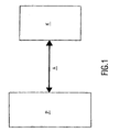
- Fig. 1 shows, in the form of a schematic block diagram, the conventional connection according to the prior art, mediated by the mapping function A of the error correction code, between the physically implemented bits P and the bits K that are available to the user, which latter bits K have where necessary been error-corrected.
- error correction codes are Hamming codes.
- a Hamming code is fundamentally an error correction code in which the difference in bit structure from character to character is particularly great, in order to maximize the probability of complete correction of the character in the event of erroneous data transmission.
- the Hamming code in which check locations can be obtained from various parity checks, it is fundamentally possible to construct codes for correcting more than one error. In the Hamming code, only some of the information locations in the code word or data word are supplemented to give even parity.
- Prior art document EP 0 307 958 A2 discloses an intelligent card comprising an EEPROM (Electrically Erasable Programmable Read-Only Memory) device having a memory cell area comprising memory cells, each memory cell storing regular data therein using the conventional physical data storing states, i. e. "erased state” and "write state". Said regular data are stored by said conventional physical data storing states being mapped by means of an error correction code encoding/decoding means capable of correcting errors occuring in said regular data stored in said memory cells. Thereby each memory cell provides a further physical state, i. e. an "intermediate state” in which a memory cell voltage threshold lies outside the valid voltage threshold ranges for said conventional physical data storing states (i. e.
- said EEPROM comprises an “intermediate state” detection circuit being provided for detecting and signalling such "intermediate states” of any memory cell, the detected “intermediate states” of memory cells being input to said error correction code encoding/decoding means for detecting and correcting erroneous data.
- prior art document US 6 151 246 revealing a multibit-per-cell nonvolatile memory dividing suitable threshold voltages of memory cells into ranges corresponding to allowed states for storage of data and ranges corresponding to forbidden zones indicating a data error.
- a refresh process includes reprogramming the threshold voltage into an allowed state. Error detection and correction codes can be used to identify data errors and generate corrected data for refresh operations.
- microelectronic memory module microelectronic memory component
- redundant data encoding for detecting and/or labeling invalid states, or states that are special in some other way
- a Hamming code error correction code by means of which one erroneous bit within a data block can be corrected ⁇ what is known as single-error correction
- This further physical state (or these further physical states) is (are) expediently selected such that unavoidable physical limitations of the memory medium are taken into account; thus, for example, in an EEPROM the state in which the memory cell transistors of any one bit are switched off and only leakage currents flow can be defined as a specific exceptional or special state.
- the implementation of the error correction code and the possible reactions to the various states can be effected in hardware or in software.
- a memory block as not yet written, by defining this state as a specific exceptional or special state in the error correction code.
- the physically stable state (which could be set after a number of years if no countermeasures are taken) may be defined as "unwritten”.
- all further physical states which can be generated in a relatively simple manner by manipulation of the memory can be characterized as exceptional or special states in the error correction code. These states can then be detected unambiguously by the software and/or by the hardware of the prepaid money card, so that manipulations of the memory can be counteracted.
- Security-related data or features of a chip can also be protected by means of essentially the same method, for example by said area being designed such that in normal operation no exceptional or special states can occur, but on the other hand for example the erasure of a memory block in this area generates an exceptional or special state.
- This exceptional or special state in a security-related memory region which is preferably embedded in at least one doped receiving substrate can then be detected, and thus appropriate measures, such as a "hardware exception” or mode changes, can be performed by the controlling C[entral]P[rocessing]U[nit] in order to ensure the security of the entire memory content and chip.
- appropriate measures such as a "hardware exception” or mode changes, can be performed by the controlling C[entral]P[rocessing]U[nit] in order to ensure the security of the entire memory content and chip.
- EEPROM fuses for example configuration and trim values
- An error detection probability that is increased in accordance with the invention is also highly significant with regard to detecting and monitoring potential attacks on the memory component or memory module, since in particular memory components or memory modules in security-related applications, such as chip cards, smart card controllers or the like, are frequently the target of various possible attacks.
- an error correction circuit is often used which makes it possible, for example, to detect and correct one-bit errors.
- Such an error correction circuit is also used, in a modified form, to detect a range of possible attacks, and this allows a reaction, for instance a deactivation, of the chip.
- One possible attack is the illumination of the memory component or memory module by means of electromagnetic waves, in particular by means of light.
- electromagnetic waves in particular by means of light.
- light sensors are integrated on the chip and the sensitive parts of the circuit, along with the memory cell area, are covered to the largest possible extent with metal, in order to prevent the illumination from having any effect. Additional bits which may be used explicitly as sensor, or read accesses performed at intervals without selection of a byte, are also conceivable.
- the covering with metal does not prevent the memory component or memory module from being illuminated with light of a suitable wavelength through the substrate, that is to say "from behind”. It is also conceivable that at high intensity the metal covering is no longer sufficient. Light sensors cover only parts of the chip surface; local illumination may thus possibly not be determined at all.
- Additional bits considerably increase the surface area of the memory matrix or memory cell area, without increasing the local sensitivity compared with the particularly inventive development presented below. Additional read accesses may also detect attacks on individual bits, but are more unreliable in the case of disturbances varying over time due to the sequential performance of the two read accesses and double memory access time.
- the present invention further relates to an error correction circuit provided for the additional "life-long” detection of possible attacks on the memory component or memory module ( ⁇ "local in-time validation" by means of the error correction code, namely by means of the Hamming code, in accordance with the present invention), implemented or integrated in at least one electronic memory component or memory module of the type mentioned above and/or operating in accordance with the method of the type mentioned above.
- the Hamming code selected as error correction code which is intended to enable the correction of one-bit errors in memory cells, requires a Hamming distance of 3, that is to say that each valid code word or data word must differ from any other code word or data word in at least three bits (if two binary words of the same length, for example bytes, are compared with one another, then, in accordance with DIN 44 300, the number of bits in which the two binary words of the same length differ from one another is what is referred to as the "Hamming distance"; this is used for error detection and error correction in that data units which have arrived via the transmission path are compared with valid characters; any necessary correction of the characters is effected in accordance with the probability principle).
- a Hamming distance of 3 means that, for code words or data words having eight data bits, additionally at least four redundant bits are required (the data bits and the redundant bits together correspond, in a manner which is essential to the invention, to the physical states P, that is to say to the physical representation).
- the redundant bits computed or determined during regular programming (writing) may be physically stored in an inverted manner in the normal mode and in a noninverted manner in the test mode. Accordingly, in accordance with an advantageous development of the present error correction circuit, at least one computation unit intended for computing and/or determining redundant bits is provided, at least one multiplexing unit
- this combined data can be stored as physical data, that is to say can be physically stored.
- the correction unit computes or determines the expected redundant bits from the data bits and compares said expected redundant bits, which are independent of the (test or normal) mode, with the redundant bits which have been switched through by the multiplexing unit, said redundant bits being nonnegated in the test mode and negated in the normal mode. From this comparison, as is customary in the case of Hamming codes, any incorrect bit can be directly ascertained, and this enables direct correction by the correction unit.
- the present invention furthermore relates to the use of at least one electronic memory component or memory module of the abovementioned type in order to detect and/or label invalid physical states or physical states that are special in some other way.
- the present invention finally relates to the use of the method of the abovementioned type in order to implement at least one additional safety feature in at least one smart card, in particular in at least one smart card controller unit
- Fig. 2 shows an example of an embodiment of a method of operating an electronic memory module 100 (or electronic memory component) as shown in Fig. 3.
- physical states P representing regular data are mapped by means of a mapping function A that describes an error correction code, namely a Hamming code.
- the error correction code is then expanded so that exceptional or special states S, L in the physical area can also be detected and reacted to appropriately.
- the user can thus, for example, program or write the physical memory (cell) area 10 with the exceptional or special state "erased" ( ⁇ reference S in Figs. 2 and 4).
- a subsequent read operation ( ⁇ reference L in Figs. 2 and 4) on the same memory area 10 then leads to a suitable exception or to a suitable special case, if this exceptional or special state has not in the meantime been rewritten with regular data. This forces the user to carry out a logically correct sequence of regular programming or write operations ( ⁇ reference S in Figs. 2 and 4) and read operations ( ⁇ reference L in Figs. 2 and 4).
- the implementation as shown in Fig. 2 can also be used to detect an unauthorized external erasure for example of EPROM memory modules or EEPROM memory modules, for instance using U[ltra]V[iolet] light, as an exceptional or special state and to react to it accordingly.
- the implementation as shown in Fig. 2 can also be used to deliberately generate exceptional or special states, in which the successful end of a financial transaction on a prepaid money card is only indicated once said states have been subsequently erased.
- the error correction code is expanded, for example, in order also to detect one or more exceptional or special states.
- the error correction code programs or writes and reads the "normal" data of the user into/from the registers of the bits K, which have where necessary been error-corrected.
- the user also has the option to program or write an exceptional or special state himself. In any case, the user is informed, by means of a suitable signal, when he discovers an exceptional or special state on the physical bits P during the read operation.
- a flash memory module having a memory cell (matrix) 10 according to the present invention which is embedded in a p-doped receiving substrate 20 in the form of an HPW trough.
- bit line 14 Assigned to this memory cell (matrix) 10 are two external sources 12a, 12b, a central bit line 14, a word line 16 arranged between bit line 14 and first source 12a or second source 12b, and a control gate 18 located between bit line 14 and word line.
- the programming voltage is divided into a positive fraction and a negative fraction. This leads to the situation where the p-doped receiving substrate 20, in which the memory cells 10 are formed, can also be connected to a negative potential.
- Fig. 4 show is an example of an embodiment of an error correction circuit 200 designed in accordance with the present invention, which error correction circuit 200 is implemented and integrated in the microelectronic memory module 100 shown in Fig. 3 and is intended to detect potential light attacks, directed at the memory module 100, using the error correction code, specifically using the Hamming code, in accordance with the present invention ( ⁇ "local in-time validation for data integrity purposes, especially for security purposes").
- the error correction code namely the Hamming code, is described by the mapping function A (cf. Figs. 2 and 4).
- the error correction circuit 200 can be used to detect a corresponding illumination attack with relatively low expenditure.
- the Hamming code selected as error correction code which enables the correction of one-bit errors in the memory cell area 10, requires a Hamming distance of 3, that is to say that each valid code word or data word differs from any other code word or data word in at least three bits.
- a Hamming distance of 3 means that, for eight-bit code words or eight-bit data words D (D0, D1, D2, D3, D4, D5, D6, D7), additionally at least four redundant bits R (R0, R1, R2, R3) are required.
- the twelve-fold "and” operation is implemented in the form of a twelve-fold "and” gate G1 which has twelve inputs, namely four inputs for the four redundant bits R (R0, R1, R2, R3) and eight inputs for the eight data bits D (D0, D1, D2, D3, D4, D5, D6, D7).
- the twelve-fold "nor” operation is implemented in the form of a twelve-fold “nor” gate G0 which likewise has twelve inputs, namely four inputs for the four redundant bits R (R0, R1, R2, R3) and eight inputs for the eight data bits D (D0, D1, D2, D3, D4, D5, D6, D7).
- the method shown in Fig. 2 can be implemented as follows:
- this combined data is stored as physical data P.
- the multiplexing unit M to which the four redundant bits R: R0, R1, R2, R3 can be applied via the first data bus B1 of width 4, switches
Landscapes
- Engineering & Computer Science (AREA)
- Theoretical Computer Science (AREA)
- Quality & Reliability (AREA)
- Physics & Mathematics (AREA)
- General Engineering & Computer Science (AREA)
- General Physics & Mathematics (AREA)
- Techniques For Improving Reliability Of Storages (AREA)
- Detection And Correction Of Errors (AREA)
- Credit Cards Or The Like (AREA)
- For Increasing The Reliability Of Semiconductor Memories (AREA)
Claims (22)
- Elektronisches Speicherbauelement oder Speichermodul (100) mit- mindestens einem Speicherzellenbereich (10), in dem physische Zustände (P), die regelmäßige Daten darstellen, mit Hilfe mindestens einer Abbildungsfunktion (A) abgebildet werden, die mindestens einen Fehlerkorrekturcode beschreibt, und- mindestens einem weiteren physischen Zustand, der mindestens einen außerordentlichen oder speziellen Zustand (L, S) in dem Fehlerkorrekturcode darstellt, wobei- der Fehlerkorrekturcode als mindestens ein Hamming-Code konfiguriert ist, der-- für das Korrigieren von Ein-Bit-Fehlern in dem Speicherzellenbereich (10) ausgelegt ist und-- einen Hamming-Abstand von 3 hat, so dass sich jedes gültige Codewort oder Datenwort von jeglichem anderen Codewort oder Datenwort um mindestens drei Bits unterscheidet, wobei- für jedes Acht-Bit-Codewort oder -Datenwort (D: D0,D1,D2,D3,D4,D5,D6,D7) zusätzlich mindestens vier redundante Bits (R: R0,R1,R2,R3) vorgesehen werden, wodurch sich Zwölf-Bit-Codewörter oder -Datenwörter ergeben.
- Speicherbauelement oder Speichermodul nach Anspruch 1, dadurch gekennzeichnet, dass der Fehlerkorrekturcode bzw. die möglichen Reaktionen auf die verschiedenen physischen Zustände mit Hilfe von Hardware bzw. Software ausgeführt werden.
- Speicherbauelement oder Speichermodul nach Anspruch 1 oder 2, dadurch gekennzeichnet, dass der außerordentliche oder spezielle Zustand (L, S) in dem Fehlerkorrekturcode gegeben ist durch- das Fließen von Leckströmen, während die Speicherzellentransistoren von jeglichem Bit abgeschaltet sind,- einen Speicherblock oder Speicherzellenbereich (10), der noch nicht beschrieben wurde,- das Manipulieren des Speicherzellenbereichs (10), beispielsweise durch Bestrahlen des Speicherzellenbereichs (10) mit elektromagnetischen Teilchen oder Wellen, bzw.- das Löschen eines Speicherblocks oder Speicherzellenbereichs (10).
- Speicherbauelement oder Speichermodul nach einem der Ansprüche 1 bis 3, dadurch gekennzeichnet, dass der Hamming-Code so ausgelegt ist, dass jedes gültige Zwölf-Bit-Codewort oder -Datenwort Folgendes aufweist:- mindestens zwei gesetzte Bits (= "1 ") bzw.- mindestens zwei gelöschte Bits (= "0"),- so dass jedes gültige Zwölf-Bit-Codewort oder -Datenwort einen Mindest-Hamming-Abstand von 2 für spezielle Zustände hat,- bei denen alle Bits eines Bytes gesetzt (= "1") (Z1) sind oder- bei denen alle Bits eines Bytes gelöscht (= "0") (Z0) sind.
- Speicherbauelement oder Speichermodul nach einem der Ansprüche 1 bis 4, dadurch gekennzeichnet, dass die vier redundanten Bits (R: R0,R1,R2,R3)- in einem Testbetrieb (T), der auch Zustände umfasst, bei denen alle Bits eines Bytes gesetzt (= "1") (Z1) sind oder bei denen alle Bits eines Bytes gelöscht (= "0") (Z0) sind, folgendermaßen ausgewählt werden:-- das dritte redundante Bit (R3) entspricht der Paritätdes siebten Datenbits (D7),des sechsten Datenbits (D6),des fünften Datenbits (D5),des vierten Datenbits (D4),des ersten Datenbits (D1),-- das zweite redundante Bit (R2) entspricht der Parität (D7),des siebten Datenbitsdes sechsten Datenbits (D6),des dritten Datenbits (D3),des zweiten Datenbits (D2),des nullten Datenbits (D0),-- das erste redundante Bit (R1) entspricht der Paritätdes siebten Datenbits (D7),des fünften Datenbits (D5),des vierten Datenbits (D4),des dritten Datenbits (D3),des nullten Datenbits (D0),-- das nullte redundante Bit (R0) entspricht der Parität (D6),des sechsten Datenbitsdes vierten Datenbits (D4),des dritten Datenbits (D3),des zweiten Datenbits (D2),des ersten Datenbits (D1), bzw.- in einem Normalbetrieb (N) folgendermaßen ausgewählt werden:-- das dritte redundante Bit (R3) entspricht der negierten Paritätdes siebten Datenbits (D7),des sechsten Datenbits (D6),des fünften Datenbits (D5),des vierten Datenbits (D4),des ersten Datenbits (D1),-- das zweite redundante Bit (R2) entspricht der negierten Paritätdes siebten Datenbits (D7),des sechsten Datenbits (D6),des dritten Datenbits (D3),des zweiten Datenbits (D2),des nullten Datenbits (D0),-- das erste redundante Bit (R1) entspricht der negierten Paritätdes siebten Datenbits (D7),des fünften Datenbits (D5),des vierten Datenbits (D4),des dritten Datenbits (D3),des nullten Datenbits (D0),-- das nullte redundante Bit (R0) entspricht der negierten Paritätdes sechsten Datenbits (D6),des vierten Datenbits (D4),des dritten Datenbits (D3),des zweiten Datenbits (D2),des ersten Datenbits (D1).
- Speicherbauelement oder Speichermodul nach einem der Ansprüche 1 bis 5, dadurch gekennzeichnet, dass die Datenbits (D: D0,D1,D2,D3,D4,D5,D6,D7) und die redundanten Bits (R: R0,R1,R2,R3) zusammen den physischen Zuständen (P) entsprechen.
- Speicherbauelement oder Speichermodul nach einem der Ansprüche 1 bis 6, dadurch gekennzeichnet, dass die Speicherzellenmatrix (10)- mindestens einer Quelle (12a, 12b),- mindestens einer Bitleitung (14),- mindestens einer Wortleitung (16) und- mindestens einem Steuergatter (18)zugeordnet ist.
- Speicherbauelement oder Speichermodul nach einem der Ansprüche 1 bis 7, dadurch gekennzeichnet, dass das Speicherbauelement oder Speichermodul (100) konfiguriert ist- als ein E[rasable]P[rogrammable]R[ead]O[nly]M[emory],- als ein E[lectrically]E[rasable]P[rogrammable]R[ead]O[nly]M[emory],- als ein Flash-Speicher,- als ein R[ead]O[nly]M[emory] oder- als ein R[andom]A[ccess]M[emory].
- Speicherbauelement oder Speichermodul nach einem der Ansprüche 1 bis 8, dadurch gekennzeichnet, dass in dem elektronischen Speicherbauelement oder Speichermodul (100) eine Fehlerkorrekturschaltung (200) implementiert oder in ihm integriert ist.
- Speicherbauelement oder Speichermodul nach Anspruch 9, dadurch gekennzeichnet, dass- die Fehlerkorrekturschaltung (200) mindestens eine Recheneinheit umfasst, die für das Berechnen und Ermitteln von redundanten Bits (R: R0,R1,R2,R3) vorgesehen ist, und- dass mindestens eine Multiplexeinheit (M),- der in einem Testbetrieb (T) nicht invertierte redundante Bits zugeführt werden können bzw.- in einem Normalbetrieb (N) invertierte redundante Bits zugeführt werden können, der genannten Recheneinheit nachgeschaltet wird.
- Speicherbauelement oder Speichermodul nach Anspruch 9 oder 10, dadurch gekennzeichnet, dass die Fehlerkorrekturschaltung (200) Folgendes umfasst:- mindestens ein zwölffaches UND-Gatter (G1), dem die Datenbits (D: D0,D1,D2,D3,D4,D5,D6,D7) und die redundanten Bits (R: R0,R1,R2,R3) zugeführt werden können bzw.- mindestens ein zwölffaches NICHT-ODER-Gatter (G0), dem die Datenbits (D: D0,D1,D2,D3,D4,D5,D6,D7) und die redundanten Bits (R: R0,R1,R2,R3) zugeführt werden können,zum Erkennen des außerordentlichen oder speziellen Zustands (L, S) in dem Fehlerkorrekturcode.
- Speicherbauelement oder Speichermodul nach einem der Ansprüche 9 bis 11, dadurch gekennzeichnet, dass die Fehlerkorrekturschaltung (200) mindestens eine Multiplexeinheit (M) umfasst, der die redundanten Bits (R: R0,R1,R2,R3) zugeführt werden können, wobei die Multiplexeinheit so ausgelegt ist, dass sie- im Testbetrieb (T) die nicht negierten redundanten Bits bzw.- im Normalbetrieb (N) die negierten redundanten Bitszu mindestens einer Korrektureinheit (U) durchschaltet, die der Multiplexeinheit (M) nachgeschaltet ist.
- Speicherbauelement oder Speichermodul nach Anspruch 10 oder 12, dadurch gekennzeichnet, dass die Fehlerkorrekturschaltung (200) mindestens eine Invertereinheit (I) umfasst, die dem Eingang (EN) der Multiplexeinheit (M) vorgeschaltet ist, der für den Normalbetrieb (N) vorgesehen ist.
- Speicherbauelement oder Speichermodul nach Anspruch 12 oder 13, dadurch gekennzeichnet, dass die Korrektureinheit (U) die erwarteten redundanten Bits aus den Datenbits (D: D0,D1,D2,D3,D4,D5,D6,D7) berechnet bzw. ermittelt und diese erwarteten redundanten Bits mit den redundanten Bits (R: R0,R1,R2,R3) vergleicht, die von der Multiplexeinheit (M) durchgeschaltet wurden, wobei die genannten redundanten Bits (R: R0,R1,R2,R3) im Testbetrieb (T) nicht negiert und im Normalbetrieb (N) negiert werden.
- Verwendung von mindestens einem elektronischen Speicherbauelement oder Speichermodul (100) nach einem der Ansprüche 1 bis 14 zum Erkennen bzw. Kennzeichnen ungültiger physischer Zustände oder physischer Zustände, die auf eine andere Art speziell sind.
- Verfahren zum Betreiben mindestens eines elektronischen Speicherbauelements oder Speichermoduls, insbesondere nach mindestens einem der Ansprüche 1 bis 14, bei dem durch mindestens eine Abbildungsfunktion (A), die mindestens einen Fehlerkorrekturcode beschreibt,- physische Zustände (P), die regelmäßige Daten darstellen, abgebildet werden und- mindestens ein weiterer physischer Zustand in Form von mindestens einem außerordentlichen oder speziellen Zustand (L, S) im Fehlerkorrekturcode erkannt, codiert bzw. angezeigt werden kann, wobei- mindestens ein Hamming-Code zum Korrigieren von Ein-Bit-Fehlern in dem Speicherzellenbereich (10) und mit einem Hamming-Abstand von 3 als Fehlerkorrekturcode ausgewählt wird, so dass sich jedes gültige Codewort oder Datenwort um mindestens drei Bits von jeglichem anderen Codewort oder Datenwort unterscheidet, und wobei- für jedes Acht-Bit-Codewort oder -Datenwort (D: D0,D1,D2,D3,D4,D5,D6,D7) zusätzlich mindestens vier redundante Bits (R: R0,R1,R2,R3) vorgesehen werden, so dass Zwölf-Bit-Codewörter oder -Datenwörter gebildet werden.
- Verfahren nach Anspruch 16, dadurch gekennzeichnet, dass der weitere physische Zustand auf der Grundlage seines Bitmusters erkannt, codiert bzw. angezeigt werden kann, selbst im Fall eines Fehlererkennungs- bzw. -korrekturvorgangs, der lediglich in beschränktem Umfang für die regelmäßigen Daten verwendet werden kann.
- Verfahren nach Anspruch 16 oder 17, gekennzeichnet durch mindestens einen Codiervorgang von redundanten Daten.
- Verfahren nach einem der Ansprüche 16 bis 18, dadurch gekennzeichnet, dass der Hamming-Code so gewählt wird, dass jedes gültige Zwölf-Bit-Codewort oder - Datenwort Folgendes aufweist:- mindestens zwei gesetzte Bits (= "1") bzw.- mindestens zwei gelöschte Bits (= "0"),- so dass jedes gültige Zwölf-Bit-Codewort oder -Datenwort einen Mindest-Hamming-Abstand von 2 für spezielle Zustände hat,- bei denen alle Bits eines Bytes gesetzt (= "1") (Z1) sind oder- bei denen alle Bits eines Bytes gelöscht (= "0") (Z0) sind.
- Verfahren nach einem der Ansprüche 16 bis 19, gekennzeichnet durch- mindestens eine zwölffache UND-Operation, der die Datenbits (D: D0,D1,D2,D3,D4,D5,D6,D7) und die redundanten Bits (R: R0,R1,R2,R3) zugeführt werden können bzw.- mindestens eine zwölffache NICHT-ODER-Operation, der die Datenbits (D: D0,D1,D2,D3,D4,D5,D6,D7) und die redundanten Bits (R: R0,R1,R2,R3) zugeführt werden können,- zum Erkennen des außerordentlichen oder speziellen Zustands (L, S) in dem Fehlerkorrekturcode.
- Verfahren nach einem der Ansprüche 16 bis 20, dadurch gekennzeichnet, dass die vier redundanten Bits (R: R0,R1,R2,R3)- in einem Testbetrieb (T), der auch Zustände umfasst, bei denen alle Bits eines Bytes gesetzt (="1") (Z1) sind oder bei denen alle Bits eines Bytes gelöscht (="0") (Z0) sind, folgendermaßen ausgewählt werden:-- das dritte redundante Bit (R3) entspricht der Paritätdes siebten Datenbits (D7),des sechsten Datenbits (D6),des fünften Datenbits (D5),des vierten Datenbits (D4),des ersten Datenbits (D1),-- das zweite redundante Bit (R2) entspricht der Paritätdes siebten Datenbits (D7),des sechsten Datenbits (D6),des dritten Datenbits (D3),des zweiten Datenbits (D2),des nullten Datenbits (D0),-- das erste redundante Bit (R1) entspricht der Paritätdes siebten Datenbits (D7),des fünften Datenbits (D5),des vierten Datenbits (D4),des dritten Datenbits (D3),des nullten Datenbits (D0),-- das nullte redundante Bit (R0) entspricht der Paritätdes sechsten Datenbits (D6),des vierten Datenbits (D4),des dritten Datenbits (D3),des zweiten Datenbits (D2),des ersten Datenbits (D1), bzw.- in einem Normalbetrieb (N) folgendermaßen ausgewählt werden:-- das dritte redundante Bit (R3) entspricht der negierten Paritätdes siebten Datenbits (D7),des sechsten Datenbits (D6),des fünften Datenbits (D5),des vierten Datenbits (D4),des ersten Datenbits (D1),-- das zweite redundante Bit (R2) entspricht der negierten Paritätdes siebten Datenbits (D7),des sechsten Datenbits (D6),des dritten Datenbits (D3),des zweiten Datenbits (D2),des nullten Datenbits (D0),-- das erste redundante Bit (R1) entspricht der negierten Paritätdes siebten Datenbits (D7),des fünften Datenbits (D5),des vierten Datenbits (D4),des dritten Datenbits (D3),des nullten Datenbits (D0),-- das nullte redundante Bit (R0) entspricht der negierten Paritätdes sechsten Datenbits (D6),des vierten Datenbits (D4),des dritten Datenbits (D3),des zweiten Datenbits (D2),des ersten Datenbits (D1).
- Verfahren nach einem der Ansprüche 16 bis 20, dadurch gekennzeichnet, dass die Datenbits (D: D0,D1,D2,D3,D4,D5,D6,D7) und die redundanten Bits (R: R0,R1,R2,R3) zusammen den physischen Zuständen (P) entsprechen
Priority Applications (1)
| Application Number | Priority Date | Filing Date | Title |
|---|---|---|---|
| EP03769799A EP1565821B1 (de) | 2002-11-21 | 2003-11-10 | Elektronisches speicherbauelement oder speichermodul, und verfahren zum betreiben desselben |
Applications Claiming Priority (6)
| Application Number | Priority Date | Filing Date | Title |
|---|---|---|---|
| DE2002154324 DE10254324A1 (de) | 2002-11-21 | 2002-11-21 | Elektronisches Speicherbauteil und Verfahren zum Betreiben desselben |
| DE10254324 | 2002-11-21 | ||
| EP03100721 | 2003-03-20 | ||
| EP03100721 | 2003-03-20 | ||
| EP03769799A EP1565821B1 (de) | 2002-11-21 | 2003-11-10 | Elektronisches speicherbauelement oder speichermodul, und verfahren zum betreiben desselben |
| PCT/IB2003/005106 WO2004046927A1 (en) | 2002-11-21 | 2003-11-10 | Electronic memory component or memory module, and mehtod of operating same |
Publications (2)
| Publication Number | Publication Date |
|---|---|
| EP1565821A1 EP1565821A1 (de) | 2005-08-24 |
| EP1565821B1 true EP1565821B1 (de) | 2006-11-02 |
Family
ID=32327504
Family Applications (1)
| Application Number | Title | Priority Date | Filing Date |
|---|---|---|---|
| EP03769799A Expired - Lifetime EP1565821B1 (de) | 2002-11-21 | 2003-11-10 | Elektronisches speicherbauelement oder speichermodul, und verfahren zum betreiben desselben |
Country Status (6)
| Country | Link |
|---|---|
| EP (1) | EP1565821B1 (de) |
| JP (1) | JP2006507611A (de) |
| AT (1) | ATE344489T1 (de) |
| AU (1) | AU2003278500A1 (de) |
| DE (1) | DE60309506T2 (de) |
| WO (1) | WO2004046927A1 (de) |
Cited By (1)
| Publication number | Priority date | Publication date | Assignee | Title |
|---|---|---|---|---|
| DE102009004291A1 (de) | 2009-01-10 | 2010-07-15 | Austria Card Gmbh | Chipkarte mit Austauschindikation |
Families Citing this family (1)
| Publication number | Priority date | Publication date | Assignee | Title |
|---|---|---|---|---|
| JP2007064762A (ja) * | 2005-08-30 | 2007-03-15 | Matsushita Electric Ind Co Ltd | 半導体装置、テストモード制御回路 |
Family Cites Families (4)
| Publication number | Priority date | Publication date | Assignee | Title |
|---|---|---|---|---|
| JPS6476596A (en) * | 1987-09-18 | 1989-03-22 | Oki Electric Ind Co Ltd | Error of eeprom detecting device |
| US5771346A (en) * | 1996-10-24 | 1998-06-23 | Micron Quantum Devices, Inc. | Apparatus and method for detecting over-programming condition in multistate memory device |
| US5909449A (en) * | 1997-09-08 | 1999-06-01 | Invox Technology | Multibit-per-cell non-volatile memory with error detection and correction |
| CN1311354C (zh) * | 2001-04-24 | 2007-04-18 | 皇家菲利浦电子有限公司 | 用于闪速存储器允许可更改位的系统和存储数据的方法 |
-
2003
- 2003-11-10 AT AT03769799T patent/ATE344489T1/de not_active IP Right Cessation
- 2003-11-10 DE DE60309506T patent/DE60309506T2/de not_active Expired - Lifetime
- 2003-11-10 EP EP03769799A patent/EP1565821B1/de not_active Expired - Lifetime
- 2003-11-10 JP JP2004570315A patent/JP2006507611A/ja active Pending
- 2003-11-10 AU AU2003278500A patent/AU2003278500A1/en not_active Abandoned
- 2003-11-10 WO PCT/IB2003/005106 patent/WO2004046927A1/en not_active Ceased
Cited By (1)
| Publication number | Priority date | Publication date | Assignee | Title |
|---|---|---|---|---|
| DE102009004291A1 (de) | 2009-01-10 | 2010-07-15 | Austria Card Gmbh | Chipkarte mit Austauschindikation |
Also Published As
| Publication number | Publication date |
|---|---|
| DE60309506T2 (de) | 2007-09-06 |
| ATE344489T1 (de) | 2006-11-15 |
| JP2006507611A (ja) | 2006-03-02 |
| EP1565821A1 (de) | 2005-08-24 |
| WO2004046927A1 (en) | 2004-06-03 |
| DE60309506D1 (de) | 2006-12-14 |
| AU2003278500A1 (en) | 2004-06-15 |
Similar Documents
| Publication | Publication Date | Title |
|---|---|---|
| US5859858A (en) | Method and apparatus for correcting a multilevel cell memory by using error locating codes | |
| WO2007036834A2 (en) | Error detection / correction circuit and corresponding method | |
| US10114693B2 (en) | Memory systems and electronic systems performing an adaptive error correction operation with pre-checked error rate, and methods of operating the memory systems | |
| KR20040086923A (ko) | 에러정정기능을 가진 플래쉬메모리장치 | |
| JP2006107710A (ja) | 停電によるプログラムエラーの有無を検出することができる集積回路メモリ装置及び方法 | |
| US7178067B2 (en) | Secure EEPROM memory comprising an error correction circuit | |
| US20070283224A1 (en) | System and method for efficient uncorrectable error detection in flash memory | |
| JP6080180B2 (ja) | 不揮発性メモリでのマーカプログラミング | |
| WO2008027759A1 (en) | Allowable bit errors per sector in memory devices | |
| US12038808B2 (en) | Memory integrity check | |
| KR20030023762A (ko) | 에러 보정 방법 및 에러 보정 회로 장치 | |
| US20060076418A1 (en) | Electronic memory component or memory module, and method of operating same | |
| US7232983B2 (en) | Circuit arrangement with non-volatile memory module and method for registering light-attacks on the non-volatile memory module | |
| US20160210063A1 (en) | Data writing method and system | |
| US20060219796A1 (en) | Integrated circuit chip card capable of determining external attack | |
| US8612777B2 (en) | Apparatus and method for writing data to be stored to a predetermined memory area | |
| EP1565821A1 (de) | Elektronisches speicherbauelement oder speichermodul, und verfahren zum betreiben desselben | |
| EP4266311B1 (de) | Nichtflüchtiges speichersystem mit konfiguration zur verringerung von fehlern bei lese- und schreiboperationen | |
| CN108304277B (zh) | 闪速存储器中的纠错方法及装置 | |
| GB2342739A (en) | Memory address checking within a solid state memory device | |
| US11061760B2 (en) | Non-volatile memory | |
| JPH02146200A (ja) | 電気的に消去可能なプログラマブルロム装置 | |
| JPS61161564A (ja) | 記憶装置 | |
| JPH05217400A (ja) | 半導体記憶集積回路 | |
| JPH0380345A (ja) | 単一チップ型マイクロコンピュータ |
Legal Events
| Date | Code | Title | Description |
|---|---|---|---|
| PUAI | Public reference made under article 153(3) epc to a published international application that has entered the european phase |
Free format text: ORIGINAL CODE: 0009012 |
|
| 17P | Request for examination filed |
Effective date: 20050621 |
|
| AK | Designated contracting states |
Kind code of ref document: A1 Designated state(s): AT BE BG CH CY CZ DE DK EE ES FI FR GB GR HU IE IT LI LU MC NL PT RO SE SI SK TR |
|
| AX | Request for extension of the european patent |
Extension state: AL LT LV MK |
|
| DAX | Request for extension of the european patent (deleted) | ||
| GRAP | Despatch of communication of intention to grant a patent |
Free format text: ORIGINAL CODE: EPIDOSNIGR1 |
|
| RTI1 | Title (correction) |
Free format text: ELECTRONIC MEMORY COMPONENT OR MEMORY MODULE, AND METHOD OF OPERATING SAME |
|
| RAP1 | Party data changed (applicant data changed or rights of an application transferred) |
Owner name: PHILIPS INTELLECTUAL PROPERTY & STANDARDS GMBH Owner name: KONINKLIJKE PHILIPS ELECTRONICS N.V. |
|
| GRAS | Grant fee paid |
Free format text: ORIGINAL CODE: EPIDOSNIGR3 |
|
| GRAA | (expected) grant |
Free format text: ORIGINAL CODE: 0009210 |
|
| AK | Designated contracting states |
Kind code of ref document: B1 Designated state(s): AT BE BG CH CY CZ DE DK EE ES FI FR GB GR HU IE IT LI LU MC NL PT RO SE SI SK TR |
|
| PG25 | Lapsed in a contracting state [announced via postgrant information from national office to epo] |
Ref country code: BE Free format text: LAPSE BECAUSE OF FAILURE TO SUBMIT A TRANSLATION OF THE DESCRIPTION OR TO PAY THE FEE WITHIN THE PRESCRIBED TIME-LIMIT Effective date: 20061102 Ref country code: IT Free format text: LAPSE BECAUSE OF FAILURE TO SUBMIT A TRANSLATION OF THE DESCRIPTION OR TO PAY THE FEE WITHIN THE PRESCRIBED TIME-LIMIT;WARNING: LAPSES OF ITALIAN PATENTS WITH EFFECTIVE DATE BEFORE 2007 MAY HAVE OCCURRED AT ANY TIME BEFORE 2007. THE CORRECT EFFECTIVE DATE MAY BE DIFFERENT FROM THE ONE RECORDED. Effective date: 20061102 Ref country code: SK Free format text: LAPSE BECAUSE OF FAILURE TO SUBMIT A TRANSLATION OF THE DESCRIPTION OR TO PAY THE FEE WITHIN THE PRESCRIBED TIME-LIMIT Effective date: 20061102 Ref country code: SI Free format text: LAPSE BECAUSE OF FAILURE TO SUBMIT A TRANSLATION OF THE DESCRIPTION OR TO PAY THE FEE WITHIN THE PRESCRIBED TIME-LIMIT Effective date: 20061102 Ref country code: NL Free format text: LAPSE BECAUSE OF FAILURE TO SUBMIT A TRANSLATION OF THE DESCRIPTION OR TO PAY THE FEE WITHIN THE PRESCRIBED TIME-LIMIT Effective date: 20061102 Ref country code: RO Free format text: LAPSE BECAUSE OF FAILURE TO SUBMIT A TRANSLATION OF THE DESCRIPTION OR TO PAY THE FEE WITHIN THE PRESCRIBED TIME-LIMIT Effective date: 20061102 Ref country code: LI Free format text: LAPSE BECAUSE OF FAILURE TO SUBMIT A TRANSLATION OF THE DESCRIPTION OR TO PAY THE FEE WITHIN THE PRESCRIBED TIME-LIMIT Effective date: 20061102 Ref country code: AT Free format text: LAPSE BECAUSE OF FAILURE TO SUBMIT A TRANSLATION OF THE DESCRIPTION OR TO PAY THE FEE WITHIN THE PRESCRIBED TIME-LIMIT Effective date: 20061102 Ref country code: CZ Free format text: LAPSE BECAUSE OF FAILURE TO SUBMIT A TRANSLATION OF THE DESCRIPTION OR TO PAY THE FEE WITHIN THE PRESCRIBED TIME-LIMIT Effective date: 20061102 Ref country code: CH Free format text: LAPSE BECAUSE OF FAILURE TO SUBMIT A TRANSLATION OF THE DESCRIPTION OR TO PAY THE FEE WITHIN THE PRESCRIBED TIME-LIMIT Effective date: 20061102 Ref country code: FI Free format text: LAPSE BECAUSE OF FAILURE TO SUBMIT A TRANSLATION OF THE DESCRIPTION OR TO PAY THE FEE WITHIN THE PRESCRIBED TIME-LIMIT Effective date: 20061102 |
|
| REG | Reference to a national code |
Ref country code: GB Ref legal event code: FG4D |
|
| PG25 | Lapsed in a contracting state [announced via postgrant information from national office to epo] |
Ref country code: IE Free format text: LAPSE BECAUSE OF NON-PAYMENT OF DUE FEES Effective date: 20061110 |
|
| REG | Reference to a national code |
Ref country code: IE Ref legal event code: FG4D |
|
| PG25 | Lapsed in a contracting state [announced via postgrant information from national office to epo] |
Ref country code: MC Free format text: LAPSE BECAUSE OF NON-PAYMENT OF DUE FEES Effective date: 20061130 |
|
| REG | Reference to a national code |
Ref country code: CH Ref legal event code: EP |
|
| REF | Corresponds to: |
Ref document number: 60309506 Country of ref document: DE Date of ref document: 20061214 Kind code of ref document: P |
|
| PG25 | Lapsed in a contracting state [announced via postgrant information from national office to epo] |
Ref country code: DK Free format text: LAPSE BECAUSE OF FAILURE TO SUBMIT A TRANSLATION OF THE DESCRIPTION OR TO PAY THE FEE WITHIN THE PRESCRIBED TIME-LIMIT Effective date: 20070202 Ref country code: SE Free format text: LAPSE BECAUSE OF FAILURE TO SUBMIT A TRANSLATION OF THE DESCRIPTION OR TO PAY THE FEE WITHIN THE PRESCRIBED TIME-LIMIT Effective date: 20070202 Ref country code: BG Free format text: LAPSE BECAUSE OF FAILURE TO SUBMIT A TRANSLATION OF THE DESCRIPTION OR TO PAY THE FEE WITHIN THE PRESCRIBED TIME-LIMIT Effective date: 20070202 |
|
| PG25 | Lapsed in a contracting state [announced via postgrant information from national office to epo] |
Ref country code: ES Free format text: LAPSE BECAUSE OF FAILURE TO SUBMIT A TRANSLATION OF THE DESCRIPTION OR TO PAY THE FEE WITHIN THE PRESCRIBED TIME-LIMIT Effective date: 20070213 |
|
| PG25 | Lapsed in a contracting state [announced via postgrant information from national office to epo] |
Ref country code: PT Free format text: LAPSE BECAUSE OF FAILURE TO SUBMIT A TRANSLATION OF THE DESCRIPTION OR TO PAY THE FEE WITHIN THE PRESCRIBED TIME-LIMIT Effective date: 20070402 |
|
| NLV1 | Nl: lapsed or annulled due to failure to fulfill the requirements of art. 29p and 29m of the patents act | ||
| REG | Reference to a national code |
Ref country code: CH Ref legal event code: PL |
|
| ET | Fr: translation filed | ||
| PLBE | No opposition filed within time limit |
Free format text: ORIGINAL CODE: 0009261 |
|
| STAA | Information on the status of an ep patent application or granted ep patent |
Free format text: STATUS: NO OPPOSITION FILED WITHIN TIME LIMIT |
|
| 26N | No opposition filed |
Effective date: 20070803 |
|
| PG25 | Lapsed in a contracting state [announced via postgrant information from national office to epo] |
Ref country code: GR Free format text: LAPSE BECAUSE OF FAILURE TO SUBMIT A TRANSLATION OF THE DESCRIPTION OR TO PAY THE FEE WITHIN THE PRESCRIBED TIME-LIMIT Effective date: 20070203 |
|
| PG25 | Lapsed in a contracting state [announced via postgrant information from national office to epo] |
Ref country code: EE Free format text: LAPSE BECAUSE OF FAILURE TO SUBMIT A TRANSLATION OF THE DESCRIPTION OR TO PAY THE FEE WITHIN THE PRESCRIBED TIME-LIMIT Effective date: 20061102 |
|
| PG25 | Lapsed in a contracting state [announced via postgrant information from national office to epo] |
Ref country code: HU Free format text: LAPSE BECAUSE OF FAILURE TO SUBMIT A TRANSLATION OF THE DESCRIPTION OR TO PAY THE FEE WITHIN THE PRESCRIBED TIME-LIMIT Effective date: 20070503 Ref country code: LU Free format text: LAPSE BECAUSE OF NON-PAYMENT OF DUE FEES Effective date: 20061110 Ref country code: TR Free format text: LAPSE BECAUSE OF FAILURE TO SUBMIT A TRANSLATION OF THE DESCRIPTION OR TO PAY THE FEE WITHIN THE PRESCRIBED TIME-LIMIT Effective date: 20061102 |
|
| REG | Reference to a national code |
Ref country code: GB Ref legal event code: 732E |
|
| PG25 | Lapsed in a contracting state [announced via postgrant information from national office to epo] |
Ref country code: CY Free format text: LAPSE BECAUSE OF FAILURE TO SUBMIT A TRANSLATION OF THE DESCRIPTION OR TO PAY THE FEE WITHIN THE PRESCRIBED TIME-LIMIT Effective date: 20061102 |
|
| REG | Reference to a national code |
Ref country code: FR Ref legal event code: TP |
|
| REG | Reference to a national code |
Ref country code: FR Ref legal event code: PLFP Year of fee payment: 13 |
|
| REG | Reference to a national code |
Ref country code: FR Ref legal event code: PLFP Year of fee payment: 14 |
|
| REG | Reference to a national code |
Ref country code: FR Ref legal event code: PLFP Year of fee payment: 15 |
|
| REG | Reference to a national code |
Ref country code: FR Ref legal event code: PLFP Year of fee payment: 16 |
|
| PGFP | Annual fee paid to national office [announced via postgrant information from national office to epo] |
Ref country code: FR Payment date: 20191022 Year of fee payment: 17 |
|
| PGFP | Annual fee paid to national office [announced via postgrant information from national office to epo] |
Ref country code: GB Payment date: 20191022 Year of fee payment: 17 |
|
| PGFP | Annual fee paid to national office [announced via postgrant information from national office to epo] |
Ref country code: DE Payment date: 20201020 Year of fee payment: 18 |
|
| GBPC | Gb: european patent ceased through non-payment of renewal fee |
Effective date: 20201110 |
|
| PG25 | Lapsed in a contracting state [announced via postgrant information from national office to epo] |
Ref country code: FR Free format text: LAPSE BECAUSE OF NON-PAYMENT OF DUE FEES Effective date: 20201130 |
|
| PG25 | Lapsed in a contracting state [announced via postgrant information from national office to epo] |
Ref country code: GB Free format text: LAPSE BECAUSE OF NON-PAYMENT OF DUE FEES Effective date: 20201110 |
|
| REG | Reference to a national code |
Ref country code: DE Ref legal event code: R119 Ref document number: 60309506 Country of ref document: DE |
|
| PG25 | Lapsed in a contracting state [announced via postgrant information from national office to epo] |
Ref country code: DE Free format text: LAPSE BECAUSE OF NON-PAYMENT OF DUE FEES Effective date: 20220601 |