EP1565236B1 - Defibrillateur a etage terminal ameliore - Google Patents
Defibrillateur a etage terminal ameliore Download PDFInfo
- Publication number
- EP1565236B1 EP1565236B1 EP03779960A EP03779960A EP1565236B1 EP 1565236 B1 EP1565236 B1 EP 1565236B1 EP 03779960 A EP03779960 A EP 03779960A EP 03779960 A EP03779960 A EP 03779960A EP 1565236 B1 EP1565236 B1 EP 1565236B1
- Authority
- EP
- European Patent Office
- Prior art keywords
- current
- patient
- higher frequency
- switching
- defibrillator
- Prior art date
- Legal status (The legal status is an assumption and is not a legal conclusion. Google has not performed a legal analysis and makes no representation as to the accuracy of the status listed.)
- Expired - Lifetime
Links
Images

Classifications
-
- A—HUMAN NECESSITIES
- A61—MEDICAL OR VETERINARY SCIENCE; HYGIENE
- A61N—ELECTROTHERAPY; MAGNETOTHERAPY; RADIATION THERAPY; ULTRASOUND THERAPY
- A61N1/00—Electrotherapy; Circuits therefor
- A61N1/18—Applying electric currents by contact electrodes
- A61N1/32—Applying electric currents by contact electrodes alternating or intermittent currents
- A61N1/38—Applying electric currents by contact electrodes alternating or intermittent currents for producing shock effects
- A61N1/39—Heart defibrillators
- A61N1/3906—Heart defibrillators characterised by the form of the shockwave
- A61N1/3912—Output circuitry therefor, e.g. switches
Definitions
- the invention relates to a defibrillator with a driven via a drive circuit for delivering a biphasic defibrillation pulse, an H-bridge between a positive pole and a negative terminal of an energy storage device having power amplifier, wherein a patient circuit is formed in the at least one inductance having shunt branch and the biphasic control in known manner by changing switching arranged in the four H-legs of the H-bridge switching elements for reversing the direction of the patient flow in the transverse branch and wherein the patient current during the various phases under specification of a desired value and inclusion of a detected actual value by means of the drive circuit is controlled by driving the switching device arrangement with a higher frequency than for generating the two opposite phases.
- a defibrillator of this type is disclosed in DE 100 65 104 A1.
- an H-bridge is provided in the transverse branch in series a current sensor, an inductance in the form of a coil and the patient electrodes are arranged with the patient resistance.
- a semiconductor switch controlled by a control device is arranged, via which the patient flow in the transverse branch can be controlled in two opposite directions by means of appropriate control, as described in more detail in this application and also known per se.
- the current is controlled by comparing an actual value of the patient current with a desired value, wherein the switch arrangement is driven at a higher frequency than the frequency of the biphasic pulse in a manner specified in more detail.
- the switch arrangement is driven at a higher frequency than the frequency of the biphasic pulse in a manner specified in more detail.
- the invention has the object of providing a defibrillator of the type mentioned in such a way that a high reliability in the delivery of biphasic defibrillation pulses is achieved.
- a safe operation with a simple structure is favored in that in the shunt branch a current sensor resistor for detecting the patient current is arranged, that from the patient current, a proportional voltage is formed, amplified by means of an amplifier and as a comparison with an internal reference voltage and an external reference voltage is supplied, and that when the external reference voltage is exceeded, a drive signal of the higher frequency for opening the relevant switching element and falls below the internal reference voltage, a drive signal of higher frequency for closing the relevant switching element is formed. Compliance with a target current is achieved by specifying the inner and outer reference voltage and can be varied accordingly.
- the drive signal of the higher frequency is formed by a logic circuit.
- the logic circuit e.g. a programmable microcontroller or a switching network or switching mechanism with memory elements and logic devices into consideration.
- the measures contribute to rectifying the amplified proportional voltage before, during, or after amplification.
- a reliable function of the output stage is supported by the fact that in each case a further diode arrangement with respect to the energy storage device is arranged in each case in the reverse direction at a connection point in the transverse branch between a patient resistor and the inductor connected in series to the positive pole and on the other hand to the negative pole.
- a further diode arrangement with respect to the energy storage device is arranged in each case in the reverse direction at a connection point in the transverse branch between a patient resistor and the inductor connected in series to the positive pole and on the other hand to the negative pole.
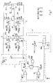
- FIG. 1 shows, as essential components here, in particular a portable externally applicable defibrillator, an output stage with an energy storage device 1 and a high-voltage part having an H-bridge 2 as well as a drive circuit 3 connected to the output stage.
- the energy storage device 1 can in the usual manner, as specified for example in the aforementioned DE 100 65 104 A1, a charging device IC and an energy storage unit C3 connected thereto, such as a capacitor arrangement having at least one capacitor or an accumulator.
- the connected to the energy storage device 1 H-bridge 2 is designed to generate biphasic defibrillation pulses, for example, with a frequency of several 100 Hz, the voltage of the pulses may be, for example, in the order of 1 kV or higher, as for example, also from the mentioned DE 100 65 104 A1.
- the biphasic pulses are thereby formed in that by driving switching elements, in particular semiconductor switching elements S1, S2, S3, S4, such as IGBTs, which are arranged in the H-legs, in the transverse branch QZ during the two phases of the defibrillation pulse
- switching elements in particular semiconductor switching elements S1, S2, S3, S4, such as IGBTs, which are arranged in the H-legs
- IGBTs IGBTs
- the H-legs directed to the positive terminal of the energy storage device 1 thus extend between a circuit point A on the side of the positive pole and circuit points B and D on the side of the shunt QZ, while the H-legs facing the negative pole of the energy storage device 1 extend from the circuit points B and D extend to the node C of the negative pole (ground) of the energy storage device 1.
- the patient resistance R5 or instead the patient electrodes are located between connection points P1, P2 of the transverse branch QZ.
- the switching elements S1, S2, S3, S4 are actuated via respective actuators U1A, U1B, U1C or U1D by means of control signals of the drive circuit 3.
- a diode arrangement DI and DII in the present case of a plurality of diodes D1, D3, D5 or . D7, D8, D10 are composed.
- the diode arrangements DI and DII block the current flow from the positive pole to the negative pole of the energy storage device 1, so that no current can flow when the switching elements S1, S2, S3, S4 are open.
- diode arrangements DIII and DIV in corresponding anti-parallel connection are arranged between the connection point P1 and the circuit point A on the one hand and the circuit point C on the other hand, these diode arrangements DIII and DIV presently also consisting of a plurality of individual diodes D2, D4, D6 and D9, D11, D12 ,
- the control element U1B of the switching element S2 between the circuit points A, B are assigned control signal inputs for signals DIG and POSh, while the control element U1D control signal inputs for control signals DIG and NEGI are assigned.
- the control element U1A of the switching element S1 arranged between the control points A and D are assigned control signal inputs for control signals MOD, NEGh, while the control element U1C for the switching element S3 between the circuit points D, C are assigned control signal inputs for control signals MOD and POSI.
- the four switching elements on the one hand suitable for forming the biphasic pulses and on the other hand for current regulation during the respective phases of opposite current direction in the transverse branch QZ are controlled, wherein the control signals DIG and MOD are formed and supplied by a current control device of the drive circuit 3.
- the current control device of the drive circuit 3 has a current feedback branch, which picks up a proportional voltage E1 across the sensor resistor R4 and supplies it to an amplifier with a circuit element U6A.
- the voltage supplied to the circuit element U6A or the amplifier thus formed is rectified by means of a switch S5, so that the voltage at the output of the amplifier to the circuit element U6A in both phases has the same polarity and applied in the same manner to comparator units U2, U5 and with whose inputs applied default values REF2 or REF1 can be compared.
- the default values represent an internal reference voltage REF1 or an external reference voltage REF2, with which a control interval for the desired current within a hysteresis band is formed.
- a desired-actual-value comparison thus takes place in both phases in a corresponding manner via the comparator units U2, U5.
- the comparison results are supplied to a memory element U4A, for example a bistable memory element (flip-flop), to whose one output a logic element U3B provided with a further control input is connected.
- the outputs of the comparator units U2, U5 provide the control signal DIG via resistors R6 and R8, while the control signal MOD is present at the output of the logic element U3B.
- the switching element S2 between the nodes A and B is permanently closed, while the switching element S3 between the nodes D and C is driven at a higher frequency of the control signal for controlling the current.
- the two other switching elements S1 between the switching points A and D and S4 between the switching points B and C are always open at this stage. This situation is illustrated in FIG. 2, wherein only the switching element S3 activated in this phase with the higher frequency is shown, since the switching element S2 is permanently closed. If the switching element S3 is closed, the patient current flows through the patient or the patient resistance R5 from the positive pole to the negative pole of the energy storage device 1.
- the switching element S3 If the switching element S3 is open, the patient current flows through the shunt QZ in the same direction, but through the first diode arrangement DI in the H-leg from the node D to A, whereby a freewheeling circuit is formed.
- the control of the switching element S3 is carried out according to the current control, wherein in the closed state of the switching element S3, the current from the energy storage C3 through the resistor R5 or the impedance of the patient, the inductance L1 and the switching element S3 increases until the means of the external reference voltage REF2 formed limit is reached.
- the switching elements S2, S3 are opened, while the switching element S4 between the points B and C is permanently closed and the switching element S1 between the points D and A of higher frequency for controlling the current is controlled.
- This situation is shown in Fig. 3, wherein only the relevant here switching element S1 is located.
- the switching element S1 is in the on state, the patient current IP flows from the energy store C3 through the switching element S1, the inductance L1 and the patient resistance R5 or the patient to ground.
- the switching element S1 When the switching element S1 is opened in this state, the patient current IP continues to flow in a corresponding direction through the patient resistance R5 or the patient, the inductance L1 and the diode arrangement DII, whereby a freewheeling circuit is likewise formed.
- This state continues until the value of the patient current IP corresponding to the internal reference voltage REF1 is reached, after which the switching element S1 is closed again by means of the current regulating circuit and so on until this opposite phase of the patient current IP or of the defibrillation pulse is terminated.
- the different pulse phases can be repeated alternately with an appropriate number.
- the current regulation can be influenced in the desired manner (determination of the width and shape of the hysteresis band), whereby reliable reliable operation of the defibrillator is achieved with the described construction of the H-bridge and its activation.
- the switching elements S2 or S4 in the H-legs in A-B or B-C, which are permanently switched on in the corresponding phases, can also be bridged with diodes DV or DVI in antiparallel arrangement, whereby negative voltage peaks in these switching elements S2 and S4 are suppressed.
Landscapes
- Health & Medical Sciences (AREA)
- Cardiology (AREA)
- Heart & Thoracic Surgery (AREA)
- Engineering & Computer Science (AREA)
- Biomedical Technology (AREA)
- Nuclear Medicine, Radiotherapy & Molecular Imaging (AREA)
- Radiology & Medical Imaging (AREA)
- Life Sciences & Earth Sciences (AREA)
- Animal Behavior & Ethology (AREA)
- General Health & Medical Sciences (AREA)
- Public Health (AREA)
- Veterinary Medicine (AREA)
- Electrotherapy Devices (AREA)
- Pharmaceuticals Containing Other Organic And Inorganic Compounds (AREA)
Claims (6)
- Défibrillateur avec un étage terminal qui est activé par l'intermédiaire d'un circuit d'activation (3) dans le but de générer une impulsion biphasée de défibrillation et qui comprend un pont en H (2) entre un pôle plus et un pôle moins d'un dispositif d'accumulation d'énergie (1), dans lequel un circuit de courant utilisé pour le patient est formé dans la branche transversale (QZ) comprenant au moins une inductance (L1) et l'activation biphasée pour inverser la direction du courant appliqué au patient (IP) a lieu dans la branche transversale (QZ) par une commutation alternative d'éléments de commutation (S1, S2, S3, S4) disposés dans les quatre branches en H du pont en H (2) et dans lequel le courant appliqué au patient (IP) est, une valeur de consigne étant imposée et une valeur réelle détectée étant intégrée, régulé lors des différentes phases au moyen du circuit d'activation (3) par l'activation de l'ensemble d'éléments de commutation (S1, S2, S3, S4) avec une fréquence plus élevée que pour la génération des deux phases opposées,
caractérisé
en ce que, pour la régulation dans l'une des directions du courant appliqué au patient (IP), seul l'élément de commutation (S3) qui est associé à cette direction du courant est activé avec la fréquence plus élevée dans la branche en H (D-C) dirigée vers le pôle moins tandis que, pour la régulation dans l'autre direction du courant appliqué au patient (IP), seul l'élément de commutation (S1) qui est associé à cette autre direction du courant est activé avec la fréquence plus élevée dans la branche en H (D-A) dirigée vers le pôle plus et
en ce que dans le sens antiparallèle par rapport aux éléments de commutation (S3, S1) activés avec une fréquence plus élevée est disposée respectivement au moins une diode (DII, DI), de sorte que, par l'intermédiaire de celle-ci et de l'élément de commutation (S2, S4) qui est fermé en permanence lors de la phase respective, le courant appliqué au patient (IP) est aussi maintenu dans sa direction respective lorsque l'élément de commutation (S3, S1) activé avec la fréquence plus élevée se trouve dans la position d'ouverture. - Défibrillateur selon la revendication 1,
caractérisé
en ce qu'une résistance de capteur de courant (R4) servant à capter le courant appliqué au patient (IP) est disposée dans la branche transversale (QZ),
en ce qu'à partir du courant appliqué au patient (IP) est formée une tension proportionnelle (E1), laquelle est amplifiée au moyen d'un amplificateur (U6A) et est amenée en tant que valeur réelle à un élément de comparaison avec une tension interne de référence (REF1) et avec une tension externe de référence (REF2) et
en ce qu'en cas de dépassement de la tension externe de référence (REF2) est formé un signal d'activation de la fréquence plus élevée pour l'ouverture de l'élément de commutation correspondant (S3, S1) et qu'en cas de non atteinte de la tension interne de référence (REF1) est formé un signal d'activation de la fréquence plus élevée pour la fermeture de l'élément de commutation correspondant (S3, S1). - Défibrillateur selon la revendication 2,
caractérisé
en ce que le signal d'activation de la fréquence plus élevée est formé par l'intermédiaire d'un circuit logique (U4A, U3B). - Défibrillateur selon la revendication 2 ou 3,
caractérisé
en ce que la tension proportionnelle amplifiée (E1) est redressée avant, pendant ou après l'amplification. - Défibrillateur selon l'une quelconque des revendications précédentes,
caractérisé
en ce qu'à un point de raccordement (P1) dans la branche transversale (QZ), entre une résistance concernant le patient (R5) et l'inductance (L1) placée en série avec celle-ci, est disposé respectivement dans le sens du blocage, d'une part en direction du pôle plus et d'autre part en direction du pôle moins, respectivement un autre agencement de diodes (DIII, DIV) se rapportant au dispositif d'accumulation d'énergie. - Défibrillateur selon l'une quelconque des revendications précédentes,
caractérisé
en ce que les deux éléments de commutation (S2, S4) sont également shuntés dans les deux autres branches en H (A-B, B-C) au moyen de diodes (DV, DVI) disposées dans le sens antiparallèle.
Applications Claiming Priority (3)
| Application Number | Priority Date | Filing Date | Title |
|---|---|---|---|
| DE10254481 | 2002-11-19 | ||
| DE10254481A DE10254481B3 (de) | 2002-11-19 | 2002-11-19 | Externer Defibrillator |
| PCT/EP2003/012857 WO2004045714A1 (fr) | 2002-11-19 | 2003-11-17 | Defibrillateur a etage terminal ameliore |
Publications (2)
| Publication Number | Publication Date |
|---|---|
| EP1565236A1 EP1565236A1 (fr) | 2005-08-24 |
| EP1565236B1 true EP1565236B1 (fr) | 2006-10-04 |
Family
ID=32318617
Family Applications (1)
| Application Number | Title | Priority Date | Filing Date |
|---|---|---|---|
| EP03779960A Expired - Lifetime EP1565236B1 (fr) | 2002-11-19 | 2003-11-17 | Defibrillateur a etage terminal ameliore |
Country Status (6)
| Country | Link |
|---|---|
| US (1) | US20060004415A1 (fr) |
| EP (1) | EP1565236B1 (fr) |
| AT (1) | ATE341365T1 (fr) |
| DE (2) | DE10254481B3 (fr) |
| ES (1) | ES2274290T3 (fr) |
| WO (1) | WO2004045714A1 (fr) |
Families Citing this family (4)
| Publication number | Priority date | Publication date | Assignee | Title |
|---|---|---|---|---|
| DE202006018672U1 (de) | 2006-12-07 | 2007-03-29 | Metrax Gmbh | Defibrillationsschock |
| DE102008034109B4 (de) * | 2008-07-21 | 2016-10-13 | Dspace Digital Signal Processing And Control Engineering Gmbh | Schaltung zur Nachbildung einer elektrischen Last |
| US10339795B2 (en) | 2013-12-24 | 2019-07-02 | Lutron Technology Company Llc | Wireless communication diagnostics |
| CN109976199B (zh) * | 2017-12-27 | 2024-05-07 | 高权 | 一种信号发生装置以及具有信号发生装置的设备 |
Family Cites Families (9)
| Publication number | Priority date | Publication date | Assignee | Title |
|---|---|---|---|---|
| EP0569616B1 (fr) * | 1992-05-12 | 1999-04-21 | Pacesetter AB | Implant pour la délivrance de impulsions électriques à un tissu vivant |
| US5725560A (en) * | 1996-06-20 | 1998-03-10 | Hewlett-Packard Company | Defibrillator with waveform selection circuitry |
| US5824017A (en) * | 1997-03-05 | 1998-10-20 | Physio-Control Corporation | H-bridge circuit for generating a high-energy biphasic waveform in an external defibrillator |
| US5873893A (en) * | 1997-03-05 | 1999-02-23 | Physio-Control Corporation | Method and apparatus for verifying the integrity of an output circuit before and during application of a defibrillation pulse |
| US6208896B1 (en) * | 1998-11-13 | 2001-03-27 | Agilent Technologies, Inc. | Method and apparatus for providing variable defibrillation waveforms using switch-mode amplification |
| US6298266B1 (en) * | 1999-08-10 | 2001-10-02 | Intermedics Inc. | Methods and apparatus for treating fibrillation and creating defibrillation waveforms |
| US20010031991A1 (en) * | 1999-12-14 | 2001-10-18 | Joseph Russial | Circuit for producing an arbitrary defibrillation waveform |
| DE10064965B4 (de) * | 1999-12-29 | 2007-01-04 | Metrax Gmbh | Medizinisches Gerät zum Beaufschlagen eines Patienten mit elektrischer Energie |
| US6421563B1 (en) * | 2000-03-01 | 2002-07-16 | Medtronic Physio-Control Manufacturing Corp. | Solid-state multiphasic defibrillation circuit |
-
2002
- 2002-11-19 DE DE10254481A patent/DE10254481B3/de not_active Expired - Fee Related
-
2003
- 2003-11-17 DE DE50305297T patent/DE50305297D1/de not_active Expired - Lifetime
- 2003-11-17 WO PCT/EP2003/012857 patent/WO2004045714A1/fr not_active Ceased
- 2003-11-17 EP EP03779960A patent/EP1565236B1/fr not_active Expired - Lifetime
- 2003-11-17 US US10/535,599 patent/US20060004415A1/en not_active Abandoned
- 2003-11-17 ES ES03779960T patent/ES2274290T3/es not_active Expired - Lifetime
- 2003-11-17 AT AT03779960T patent/ATE341365T1/de not_active IP Right Cessation
Also Published As
| Publication number | Publication date |
|---|---|
| WO2004045714A1 (fr) | 2004-06-03 |
| ATE341365T1 (de) | 2006-10-15 |
| DE10254481B3 (de) | 2004-07-15 |
| ES2274290T3 (es) | 2007-05-16 |
| US20060004415A1 (en) | 2006-01-05 |
| DE50305297D1 (de) | 2006-11-16 |
| EP1565236A1 (fr) | 2005-08-24 |
Similar Documents
| Publication | Publication Date | Title |
|---|---|---|
| DE69825568T2 (de) | Externer defibrillator mit h-brückenschaltung zur erzeugung einer zweiphasigen wellenform hoher energie | |
| DE19607704B4 (de) | Vorrichtung zur magnetischen Anregung von neuro-muskularem Gewebe | |
| DE1916088C3 (de) | Herzschrittmacher | |
| DE3036619C2 (de) | Schaltungsanordnung für den Kurzschlußschutz von Transistoren | |
| DE3882931T2 (de) | Induktiver Leistungskonverter. | |
| EP2412094B1 (fr) | Circuiterie et procédé pour fournir à un composant fonctionnel à haute énergie des impulsions de haute tension | |
| EP3332466B1 (fr) | Onduleur inverseur de polarité et avec capacité de puissance réactive ainsi que procédé d'inversion de polarité | |
| EP1565236B1 (fr) | Defibrillateur a etage terminal ameliore | |
| DE19810321C2 (de) | Verfahren und Schaltungsanordnung zur Strom- und Ladungsregelung von kapazitiven Lasten und deren Verwendung | |
| EP0893884A2 (fr) | Procédé et dispositif servant à commander un thyristor blocable | |
| EP4264649B1 (fr) | Dispositif électronique de commutation pour la démagnétisation de matériaux ferromagnétiques | |
| EP3513574B1 (fr) | Procédé et circuit destinés au fonctionnement d'un transducteur acoustique mems piézoélectrique ainsi que circuit intégré pourvu d'un tel circuit | |
| DE60100749T2 (de) | Defibrillator | |
| EP0060404B1 (fr) | Défibrillateur | |
| DE2106137A1 (de) | Herzschrittmacher | |
| DE2258862A1 (de) | Steuerschaltung zur schnellerregung elektromagnetischer systeme, insbesondere eines schrittmotors | |
| DE102017214697A1 (de) | Schaltungsanordnung und Ansteuerungsverfahren für einen piezohydraulischen Aktor | |
| DE3216911A1 (de) | Heimgeraet zur elektrotherapeutischen behandlung | |
| DE2606253C2 (fr) | ||
| EP0094341B1 (fr) | Stimulateur cardiaque | |
| DE2459810A1 (de) | Elektrischer inverter | |
| DE10065104B4 (de) | Defibrillator | |
| DE102014101319A1 (de) | Elektrozaunimpulsgenerator | |
| EP0029479A1 (fr) | Dispositif pour la stimulation électrique du coeur | |
| DE102007029767B3 (de) | Wechselrichter |
Legal Events
| Date | Code | Title | Description |
|---|---|---|---|
| PUAI | Public reference made under article 153(3) epc to a published international application that has entered the european phase |
Free format text: ORIGINAL CODE: 0009012 |
|
| 17P | Request for examination filed |
Effective date: 20050620 |
|
| AK | Designated contracting states |
Kind code of ref document: A1 Designated state(s): AT BE BG CH CY CZ DE DK EE ES FI FR GB GR HU IE IT LI LU MC NL PT RO SE SI SK TR |
|
| GRAP | Despatch of communication of intention to grant a patent |
Free format text: ORIGINAL CODE: EPIDOSNIGR1 |
|
| GRAS | Grant fee paid |
Free format text: ORIGINAL CODE: EPIDOSNIGR3 |
|
| GRAA | (expected) grant |
Free format text: ORIGINAL CODE: 0009210 |
|
| AK | Designated contracting states |
Kind code of ref document: B1 Designated state(s): AT BE BG CH CY CZ DE DK EE ES FI FR GB GR HU IE IT LI LU MC NL PT RO SE SI SK TR |
|
| PG25 | Lapsed in a contracting state [announced via postgrant information from national office to epo] |
Ref country code: SK Free format text: LAPSE BECAUSE OF FAILURE TO SUBMIT A TRANSLATION OF THE DESCRIPTION OR TO PAY THE FEE WITHIN THE PRESCRIBED TIME-LIMIT Effective date: 20061004 Ref country code: IT Free format text: LAPSE BECAUSE OF FAILURE TO SUBMIT A TRANSLATION OF THE DESCRIPTION OR TO PAY THE FEE WITHIN THE PRESCRIBED TIME-LIMIT;WARNING: LAPSES OF ITALIAN PATENTS WITH EFFECTIVE DATE BEFORE 2007 MAY HAVE OCCURRED AT ANY TIME BEFORE 2007. THE CORRECT EFFECTIVE DATE MAY BE DIFFERENT FROM THE ONE RECORDED. Effective date: 20061004 Ref country code: IE Free format text: LAPSE BECAUSE OF FAILURE TO SUBMIT A TRANSLATION OF THE DESCRIPTION OR TO PAY THE FEE WITHIN THE PRESCRIBED TIME-LIMIT Effective date: 20061004 Ref country code: SI Free format text: LAPSE BECAUSE OF FAILURE TO SUBMIT A TRANSLATION OF THE DESCRIPTION OR TO PAY THE FEE WITHIN THE PRESCRIBED TIME-LIMIT Effective date: 20061004 Ref country code: CZ Free format text: LAPSE BECAUSE OF FAILURE TO SUBMIT A TRANSLATION OF THE DESCRIPTION OR TO PAY THE FEE WITHIN THE PRESCRIBED TIME-LIMIT Effective date: 20061004 Ref country code: RO Free format text: LAPSE BECAUSE OF FAILURE TO SUBMIT A TRANSLATION OF THE DESCRIPTION OR TO PAY THE FEE WITHIN THE PRESCRIBED TIME-LIMIT Effective date: 20061004 Ref country code: NL Free format text: LAPSE BECAUSE OF FAILURE TO SUBMIT A TRANSLATION OF THE DESCRIPTION OR TO PAY THE FEE WITHIN THE PRESCRIBED TIME-LIMIT Effective date: 20061004 Ref country code: FI Free format text: LAPSE BECAUSE OF FAILURE TO SUBMIT A TRANSLATION OF THE DESCRIPTION OR TO PAY THE FEE WITHIN THE PRESCRIBED TIME-LIMIT Effective date: 20061004 |
|
| REG | Reference to a national code |
Ref country code: GB Ref legal event code: FG4D Free format text: NOT ENGLISH |
|
| REG | Reference to a national code |
Ref country code: CH Ref legal event code: EP |
|
| REG | Reference to a national code |
Ref country code: IE Ref legal event code: FG4D Free format text: LANGUAGE OF EP DOCUMENT: GERMAN |
|
| REF | Corresponds to: |
Ref document number: 50305297 Country of ref document: DE Date of ref document: 20061116 Kind code of ref document: P |
|
| PG25 | Lapsed in a contracting state [announced via postgrant information from national office to epo] |
Ref country code: BE Free format text: LAPSE BECAUSE OF NON-PAYMENT OF DUE FEES Effective date: 20061130 Ref country code: MC Free format text: LAPSE BECAUSE OF NON-PAYMENT OF DUE FEES Effective date: 20061130 |
|
| PG25 | Lapsed in a contracting state [announced via postgrant information from national office to epo] |
Ref country code: SE Free format text: LAPSE BECAUSE OF FAILURE TO SUBMIT A TRANSLATION OF THE DESCRIPTION OR TO PAY THE FEE WITHIN THE PRESCRIBED TIME-LIMIT Effective date: 20070104 Ref country code: BG Free format text: LAPSE BECAUSE OF FAILURE TO SUBMIT A TRANSLATION OF THE DESCRIPTION OR TO PAY THE FEE WITHIN THE PRESCRIBED TIME-LIMIT Effective date: 20070104 Ref country code: DK Free format text: LAPSE BECAUSE OF FAILURE TO SUBMIT A TRANSLATION OF THE DESCRIPTION OR TO PAY THE FEE WITHIN THE PRESCRIBED TIME-LIMIT Effective date: 20070104 |
|
| REG | Reference to a national code |
Ref country code: CH Ref legal event code: NV Representative=s name: SCHNEIDER FELDMANN AG PATENT- UND MARKENANWAELTE |
|
| PG25 | Lapsed in a contracting state [announced via postgrant information from national office to epo] |
Ref country code: PT Free format text: LAPSE BECAUSE OF FAILURE TO SUBMIT A TRANSLATION OF THE DESCRIPTION OR TO PAY THE FEE WITHIN THE PRESCRIBED TIME-LIMIT Effective date: 20070316 |
|
| NLV1 | Nl: lapsed or annulled due to failure to fulfill the requirements of art. 29p and 29m of the patents act | ||
| GBV | Gb: ep patent (uk) treated as always having been void in accordance with gb section 77(7)/1977 [no translation filed] |
Effective date: 20061004 |
|
| ET | Fr: translation filed | ||
| REG | Reference to a national code |
Ref country code: ES Ref legal event code: FG2A Ref document number: 2274290 Country of ref document: ES Kind code of ref document: T3 |
|
| REG | Reference to a national code |
Ref country code: IE Ref legal event code: FD4D |
|
| PLBE | No opposition filed within time limit |
Free format text: ORIGINAL CODE: 0009261 |
|
| STAA | Information on the status of an ep patent application or granted ep patent |
Free format text: STATUS: NO OPPOSITION FILED WITHIN TIME LIMIT |
|
| 26N | No opposition filed |
Effective date: 20070705 |
|
| PG25 | Lapsed in a contracting state [announced via postgrant information from national office to epo] |
Ref country code: GB Free format text: LAPSE BECAUSE OF FAILURE TO SUBMIT A TRANSLATION OF THE DESCRIPTION OR TO PAY THE FEE WITHIN THE PRESCRIBED TIME-LIMIT Effective date: 20061004 |
|
| BERE | Be: lapsed |
Owner name: METRAX G.M.B.H. Effective date: 20061130 |
|
| PG25 | Lapsed in a contracting state [announced via postgrant information from national office to epo] |
Ref country code: AT Free format text: LAPSE BECAUSE OF NON-PAYMENT OF DUE FEES Effective date: 20061117 |
|
| PG25 | Lapsed in a contracting state [announced via postgrant information from national office to epo] |
Ref country code: GR Free format text: LAPSE BECAUSE OF FAILURE TO SUBMIT A TRANSLATION OF THE DESCRIPTION OR TO PAY THE FEE WITHIN THE PRESCRIBED TIME-LIMIT Effective date: 20070105 |
|
| PG25 | Lapsed in a contracting state [announced via postgrant information from national office to epo] |
Ref country code: EE Free format text: LAPSE BECAUSE OF FAILURE TO SUBMIT A TRANSLATION OF THE DESCRIPTION OR TO PAY THE FEE WITHIN THE PRESCRIBED TIME-LIMIT Effective date: 20061004 |
|
| PG25 | Lapsed in a contracting state [announced via postgrant information from national office to epo] |
Ref country code: TR Free format text: LAPSE BECAUSE OF FAILURE TO SUBMIT A TRANSLATION OF THE DESCRIPTION OR TO PAY THE FEE WITHIN THE PRESCRIBED TIME-LIMIT Effective date: 20061004 Ref country code: HU Free format text: LAPSE BECAUSE OF FAILURE TO SUBMIT A TRANSLATION OF THE DESCRIPTION OR TO PAY THE FEE WITHIN THE PRESCRIBED TIME-LIMIT Effective date: 20070405 Ref country code: LU Free format text: LAPSE BECAUSE OF NON-PAYMENT OF DUE FEES Effective date: 20061117 |
|
| PG25 | Lapsed in a contracting state [announced via postgrant information from national office to epo] |
Ref country code: CY Free format text: LAPSE BECAUSE OF FAILURE TO SUBMIT A TRANSLATION OF THE DESCRIPTION OR TO PAY THE FEE WITHIN THE PRESCRIBED TIME-LIMIT Effective date: 20061004 |
|
| REG | Reference to a national code |
Ref country code: FR Ref legal event code: PLFP Year of fee payment: 13 |
|
| REG | Reference to a national code |
Ref country code: FR Ref legal event code: PLFP Year of fee payment: 14 |
|
| REG | Reference to a national code |
Ref country code: FR Ref legal event code: PLFP Year of fee payment: 15 |
|
| PGFP | Annual fee paid to national office [announced via postgrant information from national office to epo] |
Ref country code: ES Payment date: 20191220 Year of fee payment: 17 Ref country code: FR Payment date: 20191120 Year of fee payment: 17 Ref country code: IT Payment date: 20191128 Year of fee payment: 17 |
|
| PGFP | Annual fee paid to national office [announced via postgrant information from national office to epo] |
Ref country code: CH Payment date: 20191121 Year of fee payment: 17 |
|
| REG | Reference to a national code |
Ref country code: CH Ref legal event code: PFA Owner name: METRAX GMBH, DE Free format text: FORMER OWNER: METRAX GMBH, DE |
|
| REG | Reference to a national code |
Ref country code: CH Ref legal event code: PL |
|
| PG25 | Lapsed in a contracting state [announced via postgrant information from national office to epo] |
Ref country code: LI Free format text: LAPSE BECAUSE OF NON-PAYMENT OF DUE FEES Effective date: 20201130 Ref country code: CH Free format text: LAPSE BECAUSE OF NON-PAYMENT OF DUE FEES Effective date: 20201130 |
|
| PG25 | Lapsed in a contracting state [announced via postgrant information from national office to epo] |
Ref country code: IT Free format text: LAPSE BECAUSE OF NON-PAYMENT OF DUE FEES Effective date: 20201117 Ref country code: FR Free format text: LAPSE BECAUSE OF NON-PAYMENT OF DUE FEES Effective date: 20201130 |
|
| PGFP | Annual fee paid to national office [announced via postgrant information from national office to epo] |
Ref country code: DE Payment date: 20211129 Year of fee payment: 19 |
|
| REG | Reference to a national code |
Ref country code: ES Ref legal event code: FD2A Effective date: 20220202 |
|
| PG25 | Lapsed in a contracting state [announced via postgrant information from national office to epo] |
Ref country code: ES Free format text: LAPSE BECAUSE OF NON-PAYMENT OF DUE FEES Effective date: 20201118 |
|
| REG | Reference to a national code |
Ref country code: DE Ref legal event code: R119 Ref document number: 50305297 Country of ref document: DE |
|
| PG25 | Lapsed in a contracting state [announced via postgrant information from national office to epo] |
Ref country code: DE Free format text: LAPSE BECAUSE OF NON-PAYMENT OF DUE FEES Effective date: 20230601 |