EP1564761A1 - Laminated coil component and method of producing the same - Google Patents
Laminated coil component and method of producing the same Download PDFInfo
- Publication number
- EP1564761A1 EP1564761A1 EP04746222A EP04746222A EP1564761A1 EP 1564761 A1 EP1564761 A1 EP 1564761A1 EP 04746222 A EP04746222 A EP 04746222A EP 04746222 A EP04746222 A EP 04746222A EP 1564761 A1 EP1564761 A1 EP 1564761A1
- Authority
- EP
- European Patent Office
- Prior art keywords
- coil
- holes
- via holes
- axial direction
- opening
- Prior art date
- Legal status (The legal status is an assumption and is not a legal conclusion. Google has not performed a legal analysis and makes no representation as to the accuracy of the status listed.)
- Withdrawn
Links
Images




Classifications
-
- H—ELECTRICITY
- H01—ELECTRIC ELEMENTS
- H01F—MAGNETS; INDUCTANCES; TRANSFORMERS; SELECTION OF MATERIALS FOR THEIR MAGNETIC PROPERTIES
- H01F17/00—Fixed inductances of the signal type
- H01F17/0006—Printed inductances
- H01F17/0033—Printed inductances with the coil helically wound around a magnetic core
-
- H—ELECTRICITY
- H01—ELECTRIC ELEMENTS
- H01F—MAGNETS; INDUCTANCES; TRANSFORMERS; SELECTION OF MATERIALS FOR THEIR MAGNETIC PROPERTIES
- H01F17/00—Fixed inductances of the signal type
- H01F17/0006—Printed inductances
- H01F17/0013—Printed inductances with stacked layers
-
- H—ELECTRICITY
- H01—ELECTRIC ELEMENTS
- H01F—MAGNETS; INDUCTANCES; TRANSFORMERS; SELECTION OF MATERIALS FOR THEIR MAGNETIC PROPERTIES
- H01F27/00—Details of transformers or inductances, in general
- H01F27/28—Coils; Windings; Conductive connections
- H01F27/2804—Printed windings
-
- H—ELECTRICITY
- H01—ELECTRIC ELEMENTS
- H01F—MAGNETS; INDUCTANCES; TRANSFORMERS; SELECTION OF MATERIALS FOR THEIR MAGNETIC PROPERTIES
- H01F17/00—Fixed inductances of the signal type
- H01F17/0006—Printed inductances
- H01F17/0013—Printed inductances with stacked layers
- H01F2017/002—Details of via holes for interconnecting the layers
-
- Y—GENERAL TAGGING OF NEW TECHNOLOGICAL DEVELOPMENTS; GENERAL TAGGING OF CROSS-SECTIONAL TECHNOLOGIES SPANNING OVER SEVERAL SECTIONS OF THE IPC; TECHNICAL SUBJECTS COVERED BY FORMER USPC CROSS-REFERENCE ART COLLECTIONS [XRACs] AND DIGESTS
- Y10—TECHNICAL SUBJECTS COVERED BY FORMER USPC
- Y10T—TECHNICAL SUBJECTS COVERED BY FORMER US CLASSIFICATION
- Y10T29/00—Metal working
- Y10T29/49—Method of mechanical manufacture
- Y10T29/49002—Electrical device making
- Y10T29/4902—Electromagnet, transformer or inductor
Definitions
- the present invention relates to a laminated coil and a method for producing the laminated coil. More particularly, the invention relates to the shape of via holes in a laminated coil and a method for forming the via holes.
- a chip inductor disclosed in Japanese Unexamined Patent Application Publication No. 2002-252117 is widely known, and the construction of the chip inductor is shown in Fig. 9, and Fig. 10 is the exploded perspective view thereof.
- a related vertical lamination horizontal winding type chip inductor 11 has a structure in which a coil 13 wound in the direction Y perpendicular to the lamination direction X of a laminated body 12 is provided inside the laminated body 12.
- the coil 13 is constructed such that conductor patterns (belt-shaped conductors) 14 formed on laminated surfaces at fixed locations on the upper side and the lower side of the laminated body 12 are electrically connected through many via holes 15. Many of the via holes 15 are formed in the lamination direction X.
- each through-hole 17 has a substantially round flat shape and its inner surface has the same angle of inclination (taper angle) along the lamination direction X.
- the ceramic green sheets 16 constitute ceramic layers in the laminated body 12.
- Fig. 11 is a top view of the through-holes 17 and Fig. 12 shows the section of the through-holes 17 taken along line A - A in Fig. 11. That is, each through-hole 17 is constructed such that the diameter of the upper opening 17b is larger than the diameter of the lower opening 17a. Furthermore, at this time, the conductor patterns formed at the end portions on the upper side of the laminated body 12 are lead to the end faces and connected to external electrodes 18 formed so as to cover the end faces of the laminated body 12, respectively.
- the laminated body 12 when the laminated body 12 is produced, many of the ceramic green sheets in which only via holes are formed are disposed in the middle of the lamination direction X. Then, plural ceramic green sheets 16 in which conductor patterns 14 and via holes 15 are formed are disposed above and below the above-described ceramic green sheets 16. Furthermore, plural ceramic green sheets 16 in which no conductor patterns 14 or via holes 15 are formed are disposed above and below the above-described ceramic green sheets 16. Then, the ceramic green sheets 16 are attached by pressure in the lamination direction X and fired to obtain a laminated body 12. When the external electrodes 18 are formed on the end faces of the laminated body 12, a chip inductor 11 shown in Fig. 9 is completed.
- the ratio of the resistance Rdc of the portion in which the via holes 15 are formed to the DC resistance value Rdc of the whole chip inductor 11 increases. It is not avoidable that the resistance Rdc of the whole element is affected by that. Thus, in order to prevent such a drawback, it is able to be considered that the flat shape of the via holes 15 is increased and, as a result, the inner volume of the via holes 15 is increased.
- the flat shape of the via holes 15 is simply increased, since the flat shape of the via holes 15 is substantially round, the spacing between neighboring via holes 15 in the axial direction of the coil 13 is narrowed. Furthermore, when the flat shape of the via holes 15 is made larger and the spacing between via holes 15 is appropriately kept, the number of turns of the coil 13 is reduced. As a result, a large impedance cannot be obtained.
- the present invention has been made in consideration of such a drawback. It is an object of the present invention to provide a laminated coil in which, while the spacing between neighboring via holes in the axial direction of a coil is prevented from being narrowed, the inner space of each via hole can be increased and a method for producing the laminated coil.
- a laminated coil comprises via holes formed in the lamination direction of a laminated body; belt-shaped conductors which are formed on laminating surfaces of the laminated body and fixed end portions of which are connected thereto by the via holes; and a coil wound in the direction perpendicular to the lamination direction.
- the via holes are formed in each ceramic layer constituting the laminated body and are through-holes, each being filled with a conductor, lying in a row in the lamination direction; and, in each through-hole, the difference between the diameter in the axial direction of the coil on the opening surface of one opening of the ceramic layer and the diameter in the axial direction of the coil on the opening surface of the other opening is smaller than the difference between the diameter perpendicular to the axial direction of the coil on the opening surface of one opening of the ceramic layer and the diameter perpendicular to the axial direction of the coil on the opening surface of the other opening.
- the inner portion corresponding to the axial direction of the coil has a sharper angle of inclination in the lamination direction than the inner portion perpendicular to both the axial direction of the coil and the lamination direction.
- the inner portion perpendicular to both the axial direction of the coil and the lamination direction in each through-hole has a duller angle of inclination in the lamination direction than the inner portion corresponding to the axial direction of the coil.
- each through-hole has a substantially oval flat shape and the short-axis direction is in agreement with the axial direction of the coil.
- a method for producing a laminated coil according to the present invention comprises the step of forming the via holes such that, after through-holes have been formed, the through-holes are filled with a conductor.
- the difference between the diameter in the axial direction of the coil on one opening surface of the ceramic layer and the diameter in the axial direction of the coil on the other opening surface is smaller than the difference between the diameter perpendicular to the axial direction of the coil on one opening surface of the ceramic layer and the diameter perpendicular to the axial direction of the coil on the other opening surface. That is, in the laminated coil, since the via holes in which the angle of inclination is different at each direction on the inner portion are formed, when compared with the via holes in which the angle of inclination is the same all over the inner portion, the inner surface as a whole increases. As a result, the resistance Rdc of the portion where the via holes are formed is reduced.
- the spacing between neighboring via holes in the axial direction of the coil is prevented from being narrowed and the number of turns of the coil can be effectively prevented from being reduced.
- each through-hole constituting a via hole has a substantially oval flat shape and the short-axis direction is in agreement with the axial direction of the coil.
- the via holes described above can be easily formed as described above.
- the angle of inclination on the inner portion of the through-holes can be easily controlled by adjustment of the energy distribution of laser light, and accordingly, the via holes described above can be easily formed.
- Fig. 1 is a perspective view showing the construction of a chip inductor according to an EXAMPLE of the present invention
- Fig. 2 is an exploded perspective view showing the construction of the chip inductor of the EXAMPLE
- Fig. 3 is an enlarged perspective view showing through-holes constituting via holes in the chip inductors of the EXAMPLE.
- Fig. 4 is an enlarged top view showing the through-holes constituting via holes
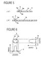
- Fig. 5A is an enlarged sectional view showing through-holes taken along line A - A in Fig. 4
- Fig. 5B is an enlarged sectional view showing through-holes, taken along line B -B in Fig. 4.
- Fig. 6 is a diagrammatical view showing the relation between a through-hole and the energy distribution of laser light
- Fig. 7 is an exploded perspective view showing the construction of a chip inductor according to a first modified example of the EXAMPLE of the present invention
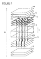
- Fig. 8 is an exploded perspective view showing the construction of a second modified example of the EXAMPLE of the present invention.
- Figs. 1 to 8 the same parts as in Figs. 9 to 12, are given the same reference numerals.
- a chip inductor 1 As shown in Figs. 1 and 2, a chip inductor 1 according to the EXAMPLE contains via holes 3 formed in the lamination direction of a laminated body 2 and conductor patterns (belt-shaped conductors) 14 in which fixed end portions are connected thereto by the via holes 3.
- a coil is constructed by the via holes and the conductor patterns formed along the laminated surfaces of the laminated body 2 and connected to the via holes.
- the coil 4 of the chip inductor 1 is constructed such that conductor patterns (belt-shaped patterns) 14 formed on the laminated surfaces at fixed locations on the upper side and the lower side of the laminated body 2 are electrically connected through many via holes 3 formed in the lamination direction X.
- the conductor patterns 14 formed at the end portions of the laminated surfaces on the upper side of the laminated body 2 are lead out to the end faces of the laminated body 2, respectively, and the conductor patterns 14 are separately connected to external electrodes 18 formed so as to cover the end faces of the laminated body 2.
- each of the conductor patterns 14 is constituted by three layers, but the conductor patterns 14 may be constituted by one layer.
- the via holes in this case are formed such that through-holes 5 are formed by laser radiation, etc., at fixed locations of each of ceramic green sheets 16 serving as ceramic layers of the laminated body 2 and the conductor-holes 5 are filled with a conductor such as conductor paste, etc.
- the through-holes 5 have an oval flat shape and their long-axis direction is a direction Z perpendicular to both the axial direction of the coil and the lamination direction X of the laminated body 2.
- the through-holes 5 are not limited to such a construction.
- the lower opening 5b of each through-hole 5 may have a substantially oval flat shape, and it is desirable that the lower opening 5b also have a substantially oval flat shape in order to reduce the resistance Rdc in the portion where the via holes are formed.
- the through-holes 5 there is provided a difference between the diameter in the axial direction of the coil 4 in one opening, that is, in the opening surface of the upper opening 5a of the ceramic green sheet 16 and the diameter in the axial direction of the coil 4 in the other opening, that is, in the opening surface of the lower opening 5b.
- the difference is made smaller than a difference between the diameter in the opening surface of the upper opening 5a in the direction Z perpendicular to both the axial direction Y of the coil 4 and the lamination direction X and the diameter in the opening surface of the lower opening 5b in the direction Z perpendicular to the axial direction Y of the coil 4 and the lamination direction X.
- the inner portion 5c corresponding to the axial direction Y of the coil 4 has a sharper angle of inclination (taper angle) than the inner portion 5d corresponding to the direction Z perpendicular to both the axial direction Y of the coil 4 and the lamination direction X of the laminated body 2.
- the inner portion 5d in the direction perpendicular to both the axial direction Y of the coil 4 and the lamination direction X has a duller angle in the lamination direction X than the inner portion 5c in the axial direction Y of the coil 4.
- the inner surface increases as a whole and the inner volume also increases.
- the resistance Rdc of the portion having a via hole 3 formed is smaller than that in the chip inductor 11 shown in the related example.
- the ratio of the resistance Rdc in the portion where the via holes are formed decreases in the whole resistance Rdc of the chip inductor 1.
- an aqueous binder such as polyvinyl acetate and water-soluble acrylic resin or an organic binder such as polyvinyl butyral is added to NiCuZn ferrite as a magnetic material.
- a dispersant, an antifoaming agent, etc., are added together with that, and then, a ceramic green sheet 16 is formed on a carrier film by using a doctor-blade coater and a reverse-roll coater.
- through-holes 5 are formed at fixed locations on the ceramic green sheets by laser radiation. Then, as shown in Fig. 6, a through-hole 5 having a substantially oval flat shape, for example, a through-hole 5 having a substantially oval upper opening 5a and a substantially round lower opening 5b is formed by adjustment of the energy distribution of laser light. That is, at this time, when the energy of laser light exceeds a threshold value S, a hole passing through the ceramic green sheet is formed, and, if the energy rapidly changes around the timing where the energy exceeds the threshold value S, the angle of inclination on the inner surface of the through-hole 5 decreases. Furthermore, if the energy slowly changes around the timing where the energy exceeds the threshold value S, the angle of inclination on the inner surface of the through-hole 5 increases.
- the dimension in the long-axis direction of the upper opening 5a of the through-hole 5, that is, in the direction perpendicular to both the axial direction Y of the coil 4 and the lamination direction X is 150 ⁇ m.
- the dimension in the short-axis direction, that is, in the short-axis direction corresponding to the axial direction Y of the coil 4 is 90 ⁇ m.
- the dimension in the long-axis direction of the lower opening 5b of the through-holes 5 is 110 ⁇ m and the dimension in the short-axis direction is 80 ⁇ m.
- the dimension in the short-axis direction of the through-holes constituting the via holes which are filled with a conductor may be made smaller. Therefore, the cases where the spacing between neighboring via holes 3 in the axial direction Y of the coil 4 becomes too small do not occur, and the outer dimensions of the laminated body 2 do not become too large. Furthermore, in the chip inductor 1 in 3216 size, when the number of turns of 25.5 is secured, the maximum dimension in the short-axis direction of the upper opening 5a of the through-holes 5 is 90 ⁇ m. That is, when the dimension in the short-axis direction of the upper opening 5a of the through-holes 5 increases, a short circuit is likely to occur because of diffused silver, cracks, etc., after sintering.
- a conductor paste having silver as the main component is prepared and the via holes 3 are formed such that the through-holes 5 formed in the ceramic green sheet 16 are filled with the conductor by screen printing of the conductor paste.
- conductor patterns 14 constituting a part of the coil 4 are formed at fixed locations on the surface of the ceramic green sheets 16. After that, as shown in Fig. 2, a fixed number of ceramic green sheets 16 in which only via holes 3 are formed are disposed in the middle of the lamination direction X. A fixed number of ceramic green sheets 16 in which via holes 3 and conductor patterns 14 are formed are disposed above and below the ceramic green sheets 16, respectively.
- a fixed number of ceramic green sheets 16 in which any of via holes 3 and conductor patterns 14 are not formed are disposed in layers above and below the ceramic green sheets 16, respectively, and then, after they have been attached by pressure in the lamination direction, they are cut so as to have fixed dimensions, they are degreased, and they are fired to obtain a laminated body 2. After that, paste is fired on both end faces of the laminated body 2, and both end faces are plated with nickel and tin to form external electrodes 18, and then, as shown in Fig. 1, a chip inductor 1 is completed.
- the chip inductor 1 in which one coil 4 is provided inside the laminated body 2 is a laminated coil, but it goes without saying that the application of the laminated coil of the present invention is not limited only to the above-described chip inductor 1. That is, a chip inductor, the structure of which is shown in Fig. 7, that is, in which two coils 4 are provided in parallel in the laminated body 2, is used as transformers and common mode choke coils. Such a chip inductor having two separate windings may be made into a laminated coil.
- the present invention may be applied to a chip inductor, the structure of which is shown in Fig. 8, that is, in which two coils 4a and 4b, alternately disposed in the lamination direction X, are provided in the laminated body 2.
- the chip inductor is constituted by alternate windings. That is, in the chip inductor, the first coil 4a is constituted by conductor patterns 14a and via holes 3a (shown by a one-dot chain line in Fig. 8), and the second coil 4b is constituted by conductor patterns 14b and via holes 3b (shown by a two-dot chain line in Fig. 8).
- the coupling coefficient between the two coils 4a and 4b in such a chip inductor of alternate windings is larger than that in the chip inductor of separate windings.
- a laminated coil of the present invention can be applied to laminated coils such as chip inductors, lamination type composite LC parts, etc.
Landscapes
- Engineering & Computer Science (AREA)
- Power Engineering (AREA)
- Microelectronics & Electronic Packaging (AREA)
- Coils Or Transformers For Communication (AREA)
- Manufacturing Cores, Coils, And Magnets (AREA)
Abstract
The inner space of each via hole can be increased while
the spacing between neighboring via holes in the axial
direction of a coil is prevented from being narrowed. In
via holes (3) of a laminated coil (1), through-holes (5)
formed in ceramic layers (16) and filled with a conductor
lie in a row in the lamination direction X, and, in each of
the through-holes (5), the difference between the diameter
in the axial direction of the coil (4) on the opening
surface of one opening (5a) of a ceramic layer (16) and the
diameter in the axial direction of the coil (4) on the
opening surface of the other opening (5b) is smaller than
the difference between the diameter in the direction Z
perpendicular to the axial direction Y of the coil (4) on
the opening surface of one opening (5a) of the ceramic layer
(16) and the diameter in the direction Z perpendicular to
the axial direction Y of the coil (4) on the opening surface
of the other opening (5b).
Description
The present invention relates to a laminated coil and a
method for producing the laminated coil. More particularly,
the invention relates to the shape of via holes in a
laminated coil and a method for forming the via holes.
As an example of a laminated coil, a chip inductor
disclosed in Japanese Unexamined Patent Application
Publication No. 2002-252117 is widely known, and the
construction of the chip inductor is shown in Fig. 9, and
Fig. 10 is the exploded perspective view thereof. As shown
in Figs. 9 and 10, a related vertical lamination horizontal
winding type chip inductor 11 has a structure in which a
coil 13 wound in the direction Y perpendicular to the
lamination direction X of a laminated body 12 is provided
inside the laminated body 12. The coil 13 is constructed
such that conductor patterns (belt-shaped conductors) 14
formed on laminated surfaces at fixed locations on the upper
side and the lower side of the laminated body 12 are
electrically connected through many via holes 15. Many of
the via holes 15 are formed in the lamination direction X.
That is, as shown in Fig. 10, these via holes 15 are
formed such that through holes 17 are formed at fixed
locations on each of ceramic green sheets 16 by laser
radiation, etc., and these through-holes 17 are filled with
a conductor such as conductor paste, etc. Then, as shown in
Figs. 11 and 12, each through-hole 17 has a substantially
round flat shape and its inner surface has the same angle of
inclination (taper angle) along the lamination direction X.
Moreover, the ceramic green sheets 16 constitute ceramic
layers in the laminated body 12.
Moreover, Fig. 11 is a top view of the through-holes 17
and Fig. 12 shows the section of the through-holes 17 taken
along line A - A in Fig. 11. That is, each through-hole 17
is constructed such that the diameter of the upper opening
17b is larger than the diameter of the lower opening 17a.
Furthermore, at this time, the conductor patterns formed at
the end portions on the upper side of the laminated body 12
are lead to the end faces and connected to external
electrodes 18 formed so as to cover the end faces of the
laminated body 12, respectively.
On the other hand, when the laminated body 12 is
produced, many of the ceramic green sheets in which only via
holes are formed are disposed in the middle of the
lamination direction X. Then, plural ceramic green sheets
16 in which conductor patterns 14 and via holes 15 are
formed are disposed above and below the above-described
ceramic green sheets 16. Furthermore, plural ceramic green
sheets 16 in which no conductor patterns 14 or via holes 15
are formed are disposed above and below the above-described
ceramic green sheets 16. Then, the ceramic green sheets 16
are attached by pressure in the lamination direction X and
fired to obtain a laminated body 12. When the external
electrodes 18 are formed on the end faces of the laminated
body 12, a chip inductor 11 shown in Fig. 9 is completed.
Now then, in the chip inductor 11, since many via holes
15 are formed, the ratio of the resistance Rdc of the
portion in which the via holes 15 are formed to the DC
resistance value Rdc of the whole chip inductor 11 increases.
It is not avoidable that the resistance Rdc of the whole
element is affected by that. Thus, in order to prevent such
a drawback, it is able to be considered that the flat shape
of the via holes 15 is increased and, as a result, the inner
volume of the via holes 15 is increased.
However, when the flat shape of the via holes 15 is
simply increased, since the flat shape of the via holes 15
is substantially round, the spacing between neighboring via
holes 15 in the axial direction of the coil 13 is narrowed.
Furthermore, when the flat shape of the via holes 15 is made
larger and the spacing between via holes 15 is appropriately
kept, the number of turns of the coil 13 is reduced. As a
result, a large impedance cannot be obtained.
The present invention has been made in consideration of
such a drawback. It is an object of the present invention
to provide a laminated coil in which, while the spacing
between neighboring via holes in the axial direction of a
coil is prevented from being narrowed, the inner space of
each via hole can be increased and a method for producing
the laminated coil.
A laminated coil comprises via holes formed in the
lamination direction of a laminated body; belt-shaped
conductors which are formed on laminating surfaces of the
laminated body and fixed end portions of which are connected
thereto by the via holes; and a coil wound in the direction
perpendicular to the lamination direction. In the laminated
coil, the via holes are formed in each ceramic layer
constituting the laminated body and are through-holes, each
being filled with a conductor, lying in a row in the
lamination direction; and, in each through-hole, the
difference between the diameter in the axial direction of
the coil on the opening surface of one opening of the
ceramic layer and the diameter in the axial direction of the
coil on the opening surface of the other opening is smaller
than the difference between the diameter perpendicular to
the axial direction of the coil on the opening surface of
one opening of the ceramic layer and the diameter
perpendicular to the axial direction of the coil on the
opening surface of the other opening.
For example, in these through-holes, the inner portion
corresponding to the axial direction of the coil has a
sharper angle of inclination in the lamination direction
than the inner portion perpendicular to both the axial
direction of the coil and the lamination direction. In
other words, the inner portion perpendicular to both the
axial direction of the coil and the lamination direction in
each through-hole has a duller angle of inclination in the
lamination direction than the inner portion corresponding to
the axial direction of the coil.
In the present invention, each through-hole has a
substantially oval flat shape and the short-axis direction
is in agreement with the axial direction of the coil.
A method for producing a laminated coil according to
the present invention comprises the step of forming the via
holes such that, after through-holes have been formed, the
through-holes are filled with a conductor.
In the laminated coil of the present invention, in each
through-hole constituting a via hole, the difference between
the diameter in the axial direction of the coil on one
opening surface of the ceramic layer and the diameter in the
axial direction of the coil on the other opening surface is
smaller than the difference between the diameter
perpendicular to the axial direction of the coil on one
opening surface of the ceramic layer and the diameter
perpendicular to the axial direction of the coil on the
other opening surface. That is, in the laminated coil,
since the via holes in which the angle of inclination is
different at each direction on the inner portion are formed,
when compared with the via holes in which the angle of
inclination is the same all over the inner portion, the
inner surface as a whole increases. As a result, the
resistance Rdc of the portion where the via holes are formed
is reduced.
Accordingly, the spacing between neighboring via holes
in the axial direction of the coil is prevented from being
narrowed and the number of turns of the coil can be
effectively prevented from being reduced. As a result, it
becomes possible to appropriately keep the spacing between
via holes and maintain the number of turns of the coil, and
the ratio of the resistance Rdc of the portion where the via
holes are formed decreases. Accordingly, a large impedance
can be secured.
In the laminated coil of the present invention, each
through-hole constituting a via hole has a substantially
oval flat shape and the short-axis direction is in agreement
with the axial direction of the coil. When such through-holes
are used, the via holes described above can be easily
formed as described above.
In the method for producing a laminated coil of the
present invention, the angle of inclination on the inner
portion of the through-holes can be easily controlled by
adjustment of the energy distribution of laser light, and
accordingly, the via holes described above can be easily
formed.
- 1
- chip inductor (laminated coil)
- 2
- laminated body
- 3
- via hole
- 4
- coil
- 5
- through-hole
- 5a
- upper opening
- 5b
- lower opening
- 5c
- inner portion (inner portion corresponding to the axial direction of a coil)
- 5d
- inner portion (inner portion corresponding to the direction perpendicular to both the axial direction of a coil and the lamination direction of a laminated body)
- 14
- conductor pattern (belt-shaped conductor)
- 16
- ceramic green sheet (ceramic layer)
- X
- lamination direction
- Y
- axial direction of a coil
- Z
- direction perpendicular to both the axial direction of a coil and the lamination direction of a laminated body
In the present invention, it was made possible to
attain the object of preventing the spacing between via
holes neighboring each other in the axial direction of a
coil from being narrowed and at the same time increasing the
inner space of each via hole by establishing a three-dimensional
structure of through-holes constituting via
holes.
Fig. 1 is a perspective view showing the construction
of a chip inductor according to an EXAMPLE of the present
invention, Fig. 2 is an exploded perspective view showing
the construction of the chip inductor of the EXAMPLE, and
Fig. 3 is an enlarged perspective view showing through-holes
constituting via holes in the chip inductors of the EXAMPLE.
Furthermore, Fig. 4 is an enlarged top view showing the
through-holes constituting via holes, Fig. 5A is an enlarged
sectional view showing through-holes taken along line A - A
in Fig. 4, and Fig. 5B is an enlarged sectional view showing
through-holes, taken along line B -B in Fig. 4.
Furthermore, Fig. 6 is a diagrammatical view showing
the relation between a through-hole and the energy
distribution of laser light, Fig. 7 is an exploded
perspective view showing the construction of a chip inductor
according to a first modified example of the EXAMPLE of the
present invention, and Fig. 8 is an exploded perspective
view showing the construction of a second modified example
of the EXAMPLE of the present invention. Moreover, in Figs.
1 to 8, the same parts as in Figs. 9 to 12, are given the
same reference numerals.
As shown in Figs. 1 and 2, a chip inductor 1 according
to the EXAMPLE contains via holes 3 formed in the lamination
direction of a laminated body 2 and conductor patterns
(belt-shaped conductors) 14 in which fixed end portions are
connected thereto by the via holes 3. In the laminated body
2 of the chip inductor 1, a coil is constructed by the via
holes and the conductor patterns formed along the laminated
surfaces of the laminated body 2 and connected to the via
holes.
That is, the coil 4 of the chip inductor 1 is
constructed such that conductor patterns (belt-shaped
patterns) 14 formed on the laminated surfaces at fixed
locations on the upper side and the lower side of the
laminated body 2 are electrically connected through many via
holes 3 formed in the lamination direction X. At this time,
the conductor patterns 14 formed at the end portions of the
laminated surfaces on the upper side of the laminated body 2
are lead out to the end faces of the laminated body 2,
respectively, and the conductor patterns 14 are separately
connected to external electrodes 18 formed so as to cover
the end faces of the laminated body 2. Moreover, in Fig. 2,
each of the conductor patterns 14 is constituted by three
layers, but the conductor patterns 14 may be constituted by
one layer.
On the other hand, as shown in Fig. 2, the via holes in
this case are formed such that through-holes 5 are formed by
laser radiation, etc., at fixed locations of each of ceramic
green sheets 16 serving as ceramic layers of the laminated
body 2 and the conductor-holes 5 are filled with a conductor
such as conductor paste, etc. Furthermore, at this time, as
shown in Figs. 3 and 4, the through-holes 5 have an oval
flat shape and their long-axis direction is a direction Z
perpendicular to both the axial direction of the coil and
the lamination direction X of the laminated body 2.
Moreover, in Figs. 3 and 4, only the upper openings 5a
in the through-holes 5 formed in the ceramic green sheets 16
have a substantially oval flat shape. The lower openings 5b
in the through-holes 5 in the ceramic green sheets 16 have a
round flat shape. However, the through-holes 5 are not
limited to such a construction. The lower opening 5b of
each through-hole 5 may have a substantially oval flat shape,
and it is desirable that the lower opening 5b also have a
substantially oval flat shape in order to reduce the
resistance Rdc in the portion where the via holes are formed.
In this case, as shown in Figs. 3 to 5, in the through-holes
5, there is provided a difference between the diameter
in the axial direction of the coil 4 in one opening, that is,
in the opening surface of the upper opening 5a of the
ceramic green sheet 16 and the diameter in the axial
direction of the coil 4 in the other opening, that is, in
the opening surface of the lower opening 5b. The difference
is made smaller than a difference between the diameter in
the opening surface of the upper opening 5a in the direction
Z perpendicular to both the axial direction Y of the coil 4
and the lamination direction X and the diameter in the
opening surface of the lower opening 5b in the direction Z
perpendicular to the axial direction Y of the coil 4 and the
lamination direction X.
That is, in the through-holes 5, the inner portion 5c
corresponding to the axial direction Y of the coil 4 has a
sharper angle of inclination (taper angle) than the inner
portion 5d corresponding to the direction Z perpendicular to
both the axial direction Y of the coil 4 and the lamination
direction X of the laminated body 2. In other words, in the
through-holes 5, the inner portion 5d in the direction
perpendicular to both the axial direction Y of the coil 4
and the lamination direction X has a duller angle in the
lamination direction X than the inner portion 5c in the
axial direction Y of the coil 4.
In the case of the through-holes 5 having such a three-dimensional
shape, when compared with the through-holes 17
having the three-dimensional shape shown in the related
example, the inner surface increases as a whole and the
inner volume also increases. Then, in the chip inductor 1
where the via holes 3 having the through-holes 5 filled with
a conductor therein are provided, the resistance Rdc of the
portion having a via hole 3 formed is smaller than that in
the chip inductor 11 shown in the related example. As a
result, the ratio of the resistance Rdc in the portion where
the via holes are formed decreases in the whole resistance
Rdc of the chip inductor 1.
Next, a method for producing a chip inductor 1
according to the EXAMPLE is described. First of all, an
aqueous binder such as polyvinyl acetate and water-soluble
acrylic resin or an organic binder such as polyvinyl butyral
is added to NiCuZn ferrite as a magnetic material. A
dispersant, an antifoaming agent, etc., are added together
with that, and then, a ceramic green sheet 16 is formed on a
carrier film by using a doctor-blade coater and a reverse-roll
coater.
In succession, through-holes 5 are formed at fixed
locations on the ceramic green sheets by laser radiation.
Then, as shown in Fig. 6, a through-hole 5 having a
substantially oval flat shape, for example, a through-hole 5
having a substantially oval upper opening 5a and a
substantially round lower opening 5b is formed by adjustment
of the energy distribution of laser light. That is, at this
time, when the energy of laser light exceeds a threshold
value S, a hole passing through the ceramic green sheet is
formed, and, if the energy rapidly changes around the timing
where the energy exceeds the threshold value S, the angle of
inclination on the inner surface of the through-hole 5
decreases. Furthermore, if the energy slowly changes around
the timing where the energy exceeds the threshold value S,
the angle of inclination on the inner surface of the
through-hole 5 increases.
Now then, when it is assumed that, in a chip inductor 1
in 3216 size, the number of turns of the coil 4 is 25.5 and
the through-holes 5 having the upper opening 5a and the
lower opening 5b, both having a substantially oval flat
shape, are formed, the following dimensions are obtained.
Although not illustrated, the dimension in the long-axis
direction of the upper opening 5a of the through-hole 5,
that is, in the direction perpendicular to both the axial
direction Y of the coil 4 and the lamination direction X is
150 µm. The dimension in the short-axis direction, that is,
in the short-axis direction corresponding to the axial
direction Y of the coil 4 is 90 µm. Furthermore, the
dimension in the long-axis direction of the lower opening 5b
of the through-holes 5 is 110 µm and the dimension in the
short-axis direction is 80 µm.
When constructed in this way, the dimension in the
short-axis direction of the through-holes constituting the
via holes which are filled with a conductor may be made
smaller. Therefore, the cases where the spacing between
neighboring via holes 3 in the axial direction Y of the coil
4 becomes too small do not occur, and the outer dimensions
of the laminated body 2 do not become too large.
Furthermore, in the chip inductor 1 in 3216 size, when the
number of turns of 25.5 is secured, the maximum dimension in
the short-axis direction of the upper opening 5a of the
through-holes 5 is 90 µm. That is, when the dimension in
the short-axis direction of the upper opening 5a of the
through-holes 5 increases, a short circuit is likely to
occur because of diffused silver, cracks, etc., after
sintering.
Next, a conductor paste having silver as the main
component is prepared and the via holes 3 are formed such
that the through-holes 5 formed in the ceramic green sheet
16 are filled with the conductor by screen printing of the
conductor paste. Then, conductor patterns 14 constituting a
part of the coil 4 are formed at fixed locations on the
surface of the ceramic green sheets 16. After that, as
shown in Fig. 2, a fixed number of ceramic green sheets 16
in which only via holes 3 are formed are disposed in the
middle of the lamination direction X. A fixed number of
ceramic green sheets 16 in which via holes 3 and conductor
patterns 14 are formed are disposed above and below the
ceramic green sheets 16, respectively.
Furthermore, a fixed number of ceramic green sheets 16
in which any of via holes 3 and conductor patterns 14 are
not formed are disposed in layers above and below the
ceramic green sheets 16, respectively, and then, after they
have been attached by pressure in the lamination direction,
they are cut so as to have fixed dimensions, they are
degreased, and they are fired to obtain a laminated body 2.
After that, paste is fired on both end faces of the
laminated body 2, and both end faces are plated with nickel
and tin to form external electrodes 18, and then, as shown
in Fig. 1, a chip inductor 1 is completed.
In the EXAMPLE, the chip inductor 1 in which one coil 4
is provided inside the laminated body 2 is a laminated coil,
but it goes without saying that the application of the
laminated coil of the present invention is not limited only
to the above-described chip inductor 1. That is, a chip
inductor, the structure of which is shown in Fig. 7, that is,
in which two coils 4 are provided in parallel in the
laminated body 2, is used as transformers and common mode
choke coils. Such a chip inductor having two separate
windings may be made into a laminated coil.
Furthermore, the present invention may be applied to a
chip inductor, the structure of which is shown in Fig. 8,
that is, in which two coils 4a and 4b, alternately disposed
in the lamination direction X, are provided in the laminated
body 2. The chip inductor is constituted by alternate
windings. That is, in the chip inductor, the first coil 4a
is constituted by conductor patterns 14a and via holes 3a
(shown by a one-dot chain line in Fig. 8), and the second
coil 4b is constituted by conductor patterns 14b and via
holes 3b (shown by a two-dot chain line in Fig. 8). The
coupling coefficient between the two coils 4a and 4b in such
a chip inductor of alternate windings is larger than that in
the chip inductor of separate windings.
Then, in such a chip inductor of alternate windings,
since many via holes 3 are aligned in the length direction
of the laminated body 2, the reduction in the resistance Rdc
because of the application of the present invention is
remarkable.
A laminated coil of the present invention can be
applied to laminated coils such as chip inductors,
lamination type composite LC parts, etc.
Claims (3)
- A laminated coil comprising:wherein the via holes are formed in each ceramic layer constituting the laminated body and are through-holes, each being filled with a conductor, lying in a row in the lamination direction; andvia holes formed in the lamination direction of a laminated body;belt-shaped conductors which are formed on laminating surfaces of the laminated body and fixed end portions of which are connected thereto by the via holes; anda coil wound in the direction perpendicular to the lamination direction,
wherein, in each through-hole, the difference between the diameter in the axial direction of the coil on the opening surface of one opening of the ceramic layer and the diameter in the axial direction of the coil on the opening surface of the other opening is smaller than the difference between the diameter perpendicular to the axial direction of the coil on the opening surface of one opening of the ceramic layer and the diameter perpendicular to the axial direction of the coil on the opening surface of the other opening. - A laminated coil as claimed in claim 1, wherein each through-hole has a substantially oval flat shape and the short-axis direction corresponds with the axial direction of the coil.
- A method for producing the laminated coil as claimed in claim 1 or 2, comprising the step of:forming the via holes such that, after through-holes have been formed, the through-holes are filled with a conductor.
Applications Claiming Priority (3)
| Application Number | Priority Date | Filing Date | Title |
|---|---|---|---|
| JP2003309027 | 2003-09-01 | ||
| JP2003309027 | 2003-09-01 | ||
| PCT/JP2004/008753 WO2005024863A1 (en) | 2003-09-01 | 2004-06-22 | Laminated coil component and method of producing the same |
Publications (2)
| Publication Number | Publication Date |
|---|---|
| EP1564761A1 true EP1564761A1 (en) | 2005-08-17 |
| EP1564761A4 EP1564761A4 (en) | 2010-03-31 |
Family
ID=34269539
Family Applications (1)
| Application Number | Title | Priority Date | Filing Date |
|---|---|---|---|
| EP04746222A Withdrawn EP1564761A4 (en) | 2003-09-01 | 2004-06-22 | Laminated coil component and method of producing the same |
Country Status (6)
| Country | Link |
|---|---|
| US (1) | US7167070B2 (en) |
| EP (1) | EP1564761A4 (en) |
| JP (1) | JPWO2005024863A1 (en) |
| KR (1) | KR100644790B1 (en) |
| CN (1) | CN100382207C (en) |
| WO (1) | WO2005024863A1 (en) |
Cited By (10)
| Publication number | Priority date | Publication date | Assignee | Title |
|---|---|---|---|---|
| WO2010014444A1 (en) * | 2008-07-29 | 2010-02-04 | Cooper Technologies Company | A magnetic electrical device |
| US7791445B2 (en) | 2006-09-12 | 2010-09-07 | Cooper Technologies Company | Low profile layered coil and cores for magnetic components |
| US8279037B2 (en) | 2008-07-11 | 2012-10-02 | Cooper Technologies Company | Magnetic components and methods of manufacturing the same |
| US8310332B2 (en) | 2008-10-08 | 2012-11-13 | Cooper Technologies Company | High current amorphous powder core inductor |
| US8466764B2 (en) | 2006-09-12 | 2013-06-18 | Cooper Technologies Company | Low profile layered coil and cores for magnetic components |
| US8659379B2 (en) | 2008-07-11 | 2014-02-25 | Cooper Technologies Company | Magnetic components and methods of manufacturing the same |
| US8941457B2 (en) | 2006-09-12 | 2015-01-27 | Cooper Technologies Company | Miniature power inductor and methods of manufacture |
| US9558881B2 (en) | 2008-07-11 | 2017-01-31 | Cooper Technologies Company | High current power inductor |
| US9589716B2 (en) | 2006-09-12 | 2017-03-07 | Cooper Technologies Company | Laminated magnetic component and manufacture with soft magnetic powder polymer composite sheets |
| US9859043B2 (en) | 2008-07-11 | 2018-01-02 | Cooper Technologies Company | Magnetic components and methods of manufacturing the same |
Families Citing this family (11)
| Publication number | Priority date | Publication date | Assignee | Title |
|---|---|---|---|---|
| WO2005036566A1 (en) * | 2003-10-10 | 2005-04-21 | Murata Manufacturing Co., Ltd. | Multilayer coil component and its manufacturing method |
| TW200735138A (en) * | 2005-10-05 | 2007-09-16 | Koninkl Philips Electronics Nv | Multi-layer inductive element for integrated circuit |
| CN101765893B (en) * | 2007-07-30 | 2012-10-10 | 株式会社村田制作所 | Chip Coil Components |
| JP2009111284A (en) * | 2007-10-31 | 2009-05-21 | Soshin Electric Co Ltd | Electronic components and passive components |
| JP5262775B2 (en) * | 2008-03-18 | 2013-08-14 | 株式会社村田製作所 | Multilayer electronic component and manufacturing method thereof |
| KR101116897B1 (en) * | 2010-01-06 | 2012-03-06 | 주식회사 실리콘하모니 | Solenoid inductor for frequency synthesizer in digital cmos process |
| CN102360796A (en) * | 2011-07-21 | 2012-02-22 | 电子科技大学 | Integrated transformer |
| KR20140083577A (en) * | 2012-12-26 | 2014-07-04 | 삼성전기주식회사 | Common mode filter and method of manufacturing the same |
| CN111876580B (en) * | 2016-02-09 | 2022-04-29 | 阿尔卑斯阿尔派株式会社 | Heat treatment apparatus for amorphous alloy ribbon laminate |
| JP6594837B2 (en) * | 2016-09-30 | 2019-10-23 | 太陽誘電株式会社 | Coil parts |
| WO2021100424A1 (en) * | 2019-11-22 | 2021-05-27 | 株式会社村田製作所 | Laminated coil component |
Family Cites Families (13)
| Publication number | Priority date | Publication date | Assignee | Title |
|---|---|---|---|---|
| JPS6196548A (en) | 1984-10-17 | 1986-05-15 | Clarion Co Ltd | Tape tension applying mechanism of tape recorder |
| JPS6196548U (en) * | 1984-11-30 | 1986-06-21 | ||
| US5304743A (en) * | 1992-05-12 | 1994-04-19 | Lsi Logic Corporation | Multilayer IC semiconductor package |
| US5404118A (en) * | 1992-07-27 | 1995-04-04 | Murata Manufacturing Co., Ltd. | Band pass filter with resonator having spiral electrodes formed of coil electrodes on plurality of dielectric layers |
| JPH0992753A (en) * | 1995-09-26 | 1997-04-04 | Toshiba Corp | Multilayer ceramic circuit board and manufacturing method thereof |
| JP3077056B2 (en) * | 1996-09-12 | 2000-08-14 | 株式会社村田製作所 | Multilayer electronic components |
| MY122218A (en) * | 1998-02-02 | 2006-03-31 | Taiyo Yuden Kk | Multilayer electronic component and manufacturing method therefor |
| JP3788074B2 (en) | 1998-11-10 | 2006-06-21 | 株式会社村田製作所 | Chip coil and manufacturing method thereof |
| US6249205B1 (en) * | 1998-11-20 | 2001-06-19 | Steward, Inc. | Surface mount inductor with flux gap and related fabrication methods |
| JP3571247B2 (en) * | 1999-03-31 | 2004-09-29 | 太陽誘電株式会社 | Multilayer electronic components |
| JP3562568B2 (en) * | 1999-07-16 | 2004-09-08 | 日本電気株式会社 | Multilayer wiring board |
| JP3788325B2 (en) * | 2000-12-19 | 2006-06-21 | 株式会社村田製作所 | Multilayer coil component and manufacturing method thereof |
| JP2003017325A (en) | 2001-06-27 | 2003-01-17 | Murata Mfg Co Ltd | Lamination type metal magnetic electronic component and its manufacturing method |
-
2004
- 2004-06-22 JP JP2005513599A patent/JPWO2005024863A1/en active Pending
- 2004-06-22 US US10/527,036 patent/US7167070B2/en not_active Expired - Lifetime
- 2004-06-22 CN CNB2004800007490A patent/CN100382207C/en not_active Expired - Lifetime
- 2004-06-22 KR KR1020057005488A patent/KR100644790B1/en not_active Expired - Lifetime
- 2004-06-22 WO PCT/JP2004/008753 patent/WO2005024863A1/en not_active Ceased
- 2004-06-22 EP EP04746222A patent/EP1564761A4/en not_active Withdrawn
Cited By (14)
| Publication number | Priority date | Publication date | Assignee | Title |
|---|---|---|---|---|
| US8941457B2 (en) | 2006-09-12 | 2015-01-27 | Cooper Technologies Company | Miniature power inductor and methods of manufacture |
| US8484829B2 (en) | 2006-09-12 | 2013-07-16 | Cooper Technologies Company | Methods for manufacturing magnetic components having low probile layered coil and cores |
| US8466764B2 (en) | 2006-09-12 | 2013-06-18 | Cooper Technologies Company | Low profile layered coil and cores for magnetic components |
| US9589716B2 (en) | 2006-09-12 | 2017-03-07 | Cooper Technologies Company | Laminated magnetic component and manufacture with soft magnetic powder polymer composite sheets |
| US7791445B2 (en) | 2006-09-12 | 2010-09-07 | Cooper Technologies Company | Low profile layered coil and cores for magnetic components |
| US9558881B2 (en) | 2008-07-11 | 2017-01-31 | Cooper Technologies Company | High current power inductor |
| US8279037B2 (en) | 2008-07-11 | 2012-10-02 | Cooper Technologies Company | Magnetic components and methods of manufacturing the same |
| US9859043B2 (en) | 2008-07-11 | 2018-01-02 | Cooper Technologies Company | Magnetic components and methods of manufacturing the same |
| US8659379B2 (en) | 2008-07-11 | 2014-02-25 | Cooper Technologies Company | Magnetic components and methods of manufacturing the same |
| US8378777B2 (en) | 2008-07-29 | 2013-02-19 | Cooper Technologies Company | Magnetic electrical device |
| CN102099877B (en) * | 2008-07-29 | 2015-08-12 | 库柏技术公司 | Magnetic device |
| WO2010014444A1 (en) * | 2008-07-29 | 2010-02-04 | Cooper Technologies Company | A magnetic electrical device |
| US8910373B2 (en) | 2008-07-29 | 2014-12-16 | Cooper Technologies Company | Method of manufacturing an electromagnetic component |
| US8310332B2 (en) | 2008-10-08 | 2012-11-13 | Cooper Technologies Company | High current amorphous powder core inductor |
Also Published As
| Publication number | Publication date |
|---|---|
| KR20050059214A (en) | 2005-06-17 |
| EP1564761A4 (en) | 2010-03-31 |
| US7167070B2 (en) | 2007-01-23 |
| JPWO2005024863A1 (en) | 2006-11-16 |
| WO2005024863A1 (en) | 2005-03-17 |
| CN100382207C (en) | 2008-04-16 |
| US20060152319A1 (en) | 2006-07-13 |
| KR100644790B1 (en) | 2006-11-15 |
| CN1701397A (en) | 2005-11-23 |
Similar Documents
| Publication | Publication Date | Title |
|---|---|---|
| EP1564761A1 (en) | Laminated coil component and method of producing the same | |
| US7446638B2 (en) | Multilayer inductor | |
| JP4821908B2 (en) | Multilayer electronic component and electronic component module including the same | |
| KR101956590B1 (en) | Multilayer coil component | |
| JP6500992B2 (en) | Coil built-in parts | |
| KR20140011693A (en) | Magnetic substance module for power inductor, power inductor and manufacturing method for the same | |
| JP2002319508A (en) | Laminated impedance element | |
| US6727795B2 (en) | Laminated electronic component and manufacturing method | |
| KR101156986B1 (en) | Multilayer inductor | |
| KR100453429B1 (en) | Laminated electric parts | |
| EP1367611A1 (en) | Inductor part, and method of producing the same | |
| JPH05217772A (en) | Composite laminated transformer and its production | |
| JPH06224043A (en) | Laminated chip transformer and manufacture thereof | |
| JP2005175300A (en) | Laminated ceramic electronic component | |
| JP6784183B2 (en) | Multilayer coil parts | |
| US10998129B2 (en) | Method for manufacturing laminated coil component | |
| JP2003217935A (en) | Layered inductor array | |
| US6551426B2 (en) | Manufacturing method for a laminated ceramic electronic component | |
| JP2005142389A (en) | Multilayer electronic component and manufacturing method thereof | |
| JP2000260621A (en) | Stacked type common mode choke coil | |
| JP2005259878A (en) | Laminated coil component | |
| KR20190020308A (en) | Magnetic Substance Module for Power Inductor, Power Inductor and Manufacturing Method for the Same | |
| JP2005294637A (en) | Laminated coil array | |
| JP2006352018A (en) | Multilayer electronic part | |
| JP4451077B2 (en) | Multilayer inductor |
Legal Events
| Date | Code | Title | Description |
|---|---|---|---|
| PUAI | Public reference made under article 153(3) epc to a published international application that has entered the european phase |
Free format text: ORIGINAL CODE: 0009012 |
|
| 17P | Request for examination filed |
Effective date: 20050202 |
|
| AK | Designated contracting states |
Kind code of ref document: A1 Designated state(s): AT BE BG CH CY CZ DE DK EE ES FI FR GB GR HU IE IT LI LU MC NL PL PT RO SE SI SK TR |
|
| AX | Request for extension of the european patent |
Extension state: AL HR LT LV MK |
|
| DAX | Request for extension of the european patent (deleted) | ||
| A4 | Supplementary search report drawn up and despatched |
Effective date: 20100226 |
|
| 17Q | First examination report despatched |
Effective date: 20100528 |
|
| STAA | Information on the status of an ep patent application or granted ep patent |
Free format text: STATUS: THE APPLICATION IS DEEMED TO BE WITHDRAWN |
|
| 18D | Application deemed to be withdrawn |
Effective date: 20101008 |